
Fabrication of a Micron-Scale Three-Dimensional Single Crystal Diamond Channel Using a Micro-Jet Water-Assisted Laser


Abstract
:1. Introduction
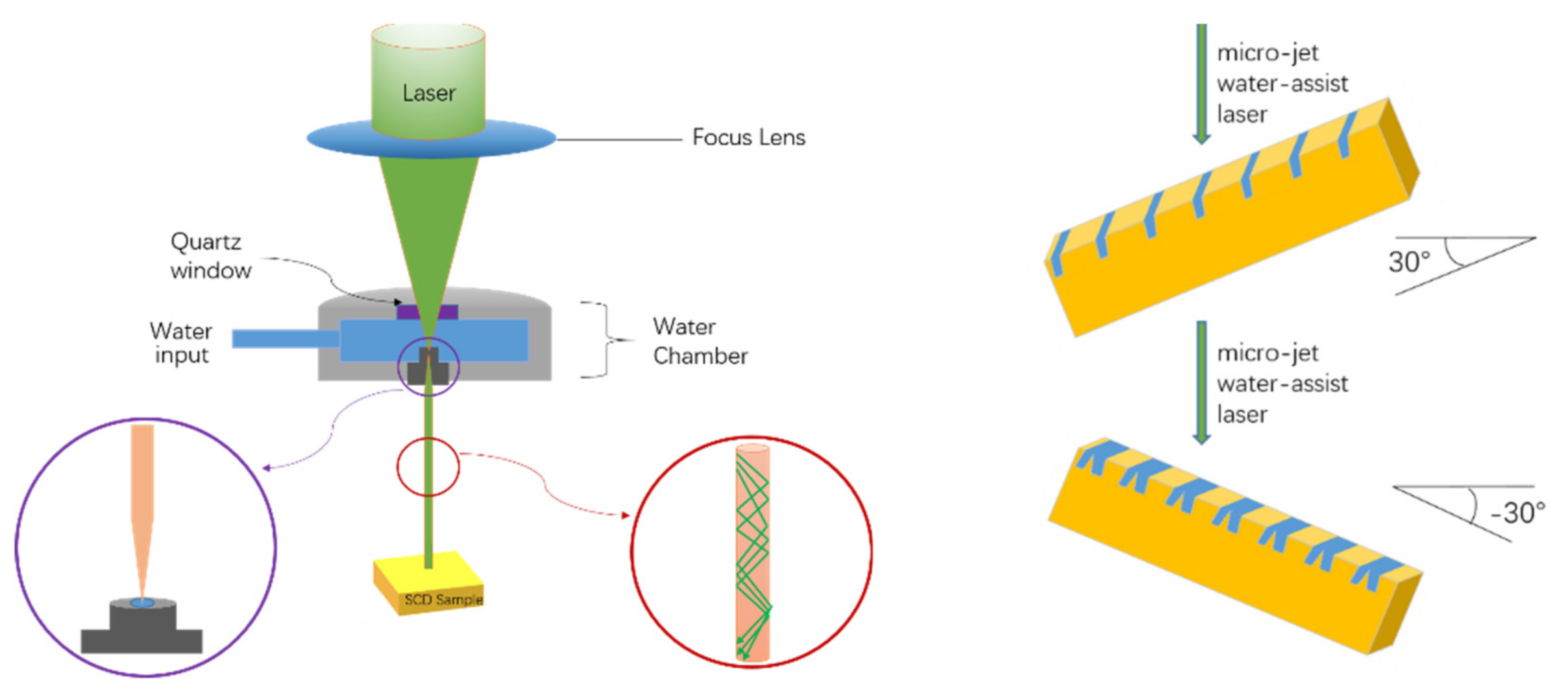
2. Experiment
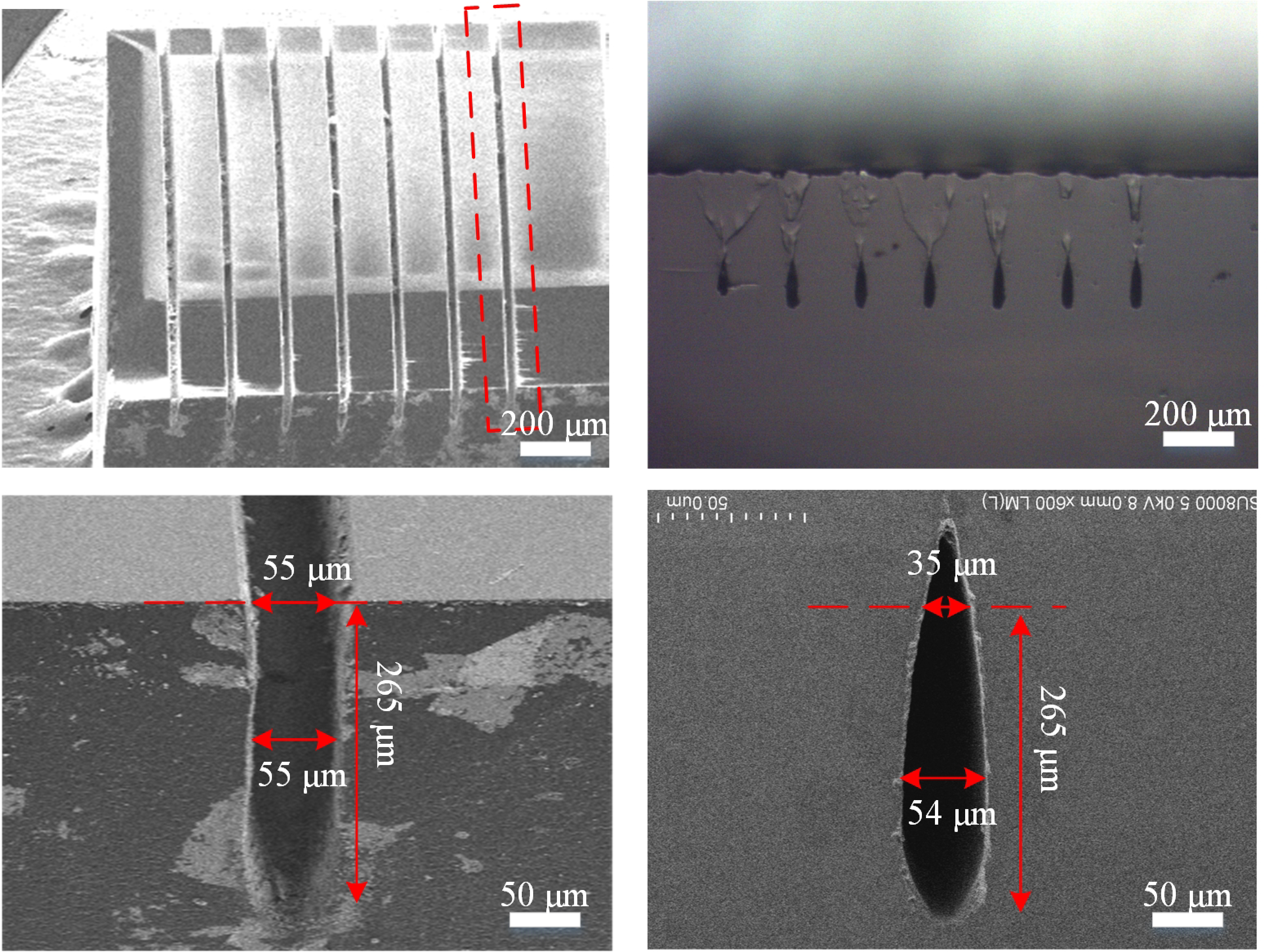
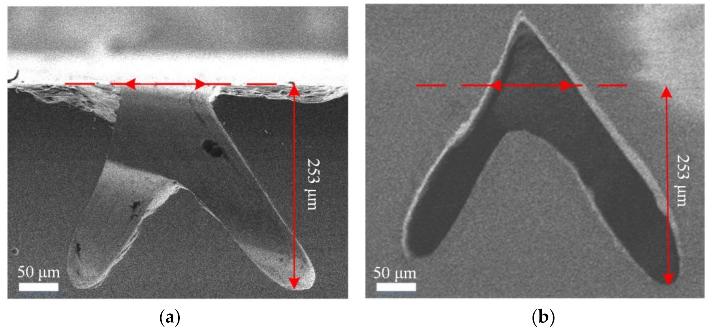
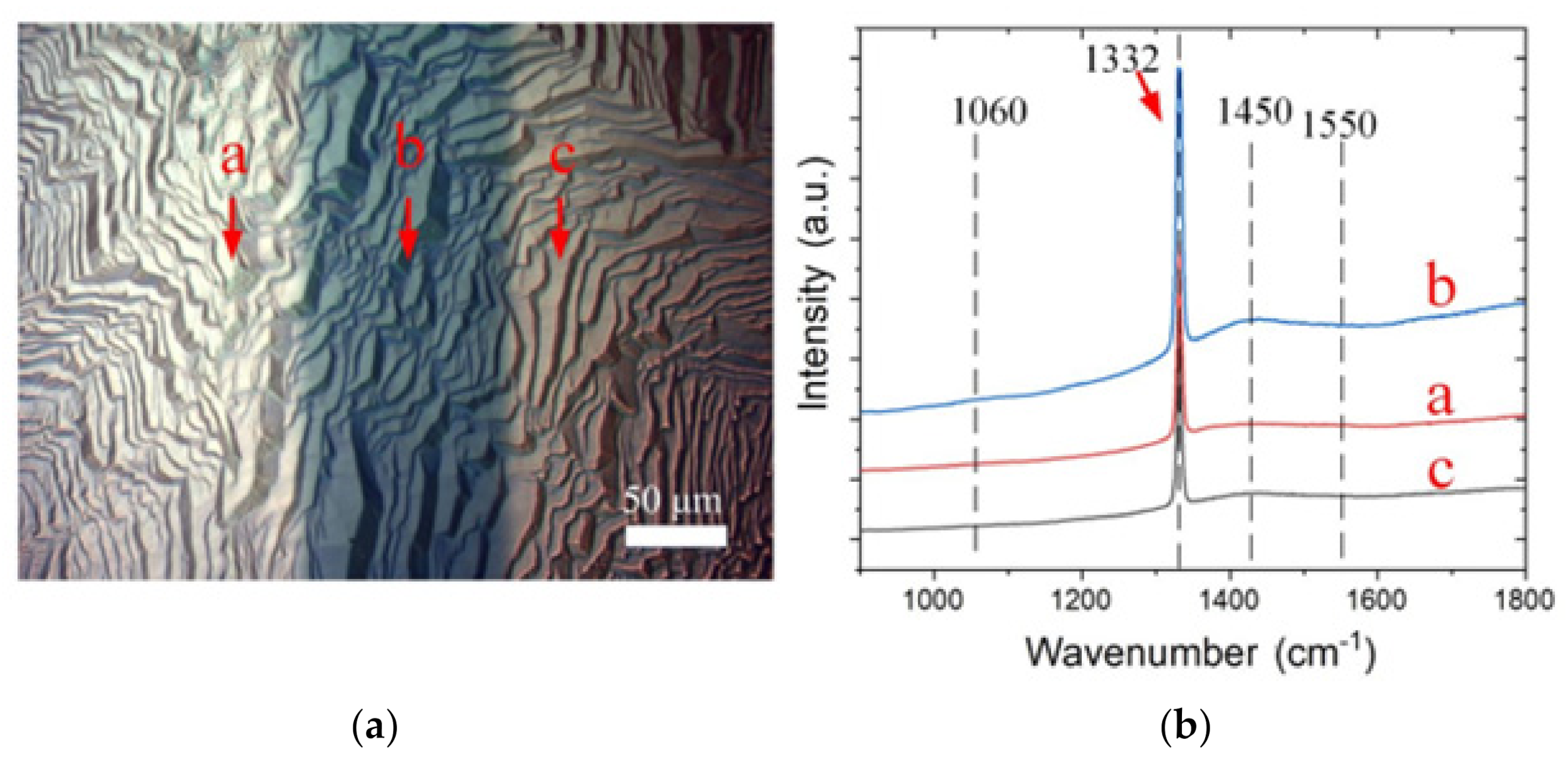
3. Results and Discussion
4. Conclusions
Author Contributions
Funding
Institutional Review Board Statement
Informed Consent Statement
Data Availability Statement
Conflicts of Interest
References
- May, P.W. Materials science: The new diamond age? Science 2008, 319, 1490–1491. [Google Scholar] [CrossRef]
- Isberg, J.; Hammersberg, J.; Bernhoff, H.; Twitchen, D.J.; Whitehead, A.J. Charge collection distance measurements in single and polycrystalline CVD diamond. Diam. Relat. Mater. 2004, 13, 872–875. [Google Scholar] [CrossRef]
- Hetsroni, G.; Mosyak, A.; Pogrebnyak, E.; Yarin, L.P. Fluid flow in micro-channels. Int. J. Heat Mass Transf. 2005, 48, 1982–1998. [Google Scholar] [CrossRef]
- Anthony, T.R.; Banholzer, W.F.; Fleischer, J.F.; Wei, L.; Kuo, P.K. Thermal diffusivity of isotopically enriched 12C diamond. Phys. Rev. B 1990, 42, 1104–1111. [Google Scholar] [CrossRef]
- Han, Y.; Lau, B.L.; Zhang, X.; Leong, Y.C.; Choo, K.F. Enhancement of hotspot cooling with diamond heat spreader on Cu microchannel heat sink for GaN-on-Si device. IEEE Trans. Compon. Packag. Manuf. Technol. 2014, 4, 983–990. [Google Scholar] [CrossRef]
- Fedorov, A.G.; Viskanta, R. Three-dimensional conjugate heat transfer in the microchannel heat sink for electronic packaging. Int. J. Heat Mass Transf. 2000, 43, 399–415. [Google Scholar] [CrossRef]
- Parasuraman, P.S.; Ho, J.H.; Lin, M.H.; Ho, C.H. In-Plane Axially Enhanced Photocatalysis by Re4 Diamond Chains in Layered ReS2. J. Phys. Chem. C 2018, 122, 18776–18784. [Google Scholar] [CrossRef]
- Su, R.; Liu, Z.; Abbasi, H.N.; Wei, J.; Wang, H. Visible-light activation of photocatalytic for reduction of nitrogen to ammonia by introducing impurity defect levels into nanocrystalline diamond. Materials 2020, 13, 4559. [Google Scholar] [CrossRef]
- Fadzin, K.A.; Lee, A. Heat transfer enhancement in microchannel using nanofluids. Appl. Mech. Mater. 2014, 465–466, 536–540. [Google Scholar] [CrossRef]
- Airoldi, F.; Colombo, A.; Tavano, D.; Stamkovic, G.; Klugmann, S.; Paolillo, V.; Bonizzoni, E.; Briguori, C.; Carlino, M.; Montorfano, M.; et al. Comparison of diamond-like carbon-coated stents versus uncoated stainless steel stents in coronary artery disease. Am. J. Cardiol. 2004, 93, 474–477. [Google Scholar] [CrossRef]
- Salahas, A.; Vrahatis, A.; Karabinos, I.; Antonellis, I.; Ifantis, G.; Gavaliatsis, I.; Anthopoulos, P.; Tavernarakis, A. Success, safety, and efficacy of implantation of diamond-like carbon-coated stents. Angiology 2007, 58, 203–210. [Google Scholar] [CrossRef] [PubMed]
- Ditalia Tchernij, S.; Skukan, N.; Picollo, F.; Battiato, A.; Grilj, V.; Amato, G.; Boarino, L.; Enrico, E.; Jaksic, M.; Olivero, P.; et al. Electrical characterization of a graphite-diamond-graphite junction fabricated by MeV carbon implantation. Diam. Relat. Mater. 2017, 74, 125–131. [Google Scholar] [CrossRef]
- Liang, Y.; Zhu, T.; Xi, M.; Abbasi, H.N.; Fu, J.; Su, R.; Song, Z.; Wang, H.; Wang, K. Fabrication of a diamond concave microlens array for laser beam homogenization. Opt. Laser Technol. 2021, 136, 106738. [Google Scholar] [CrossRef]
- Trucchi, D.M.; Bellucci, A.; Girolami, M.; Mastellone, M.; Orlando, S. Surface texturing of CVD diamond assisted by ultrashot laser pulses. Coatings 2017, 7, 185. [Google Scholar] [CrossRef] [Green Version]
- Bharadwaj, V.; Jedrkiewicz, O.; Hadden, J.P.; Sotillo, B.; Vazquez, M.R.; Dentella, P.; Fernandez, T.T.; Chiappini, A.; Giakoumaki, A.N.; Phu, T.L.; et al. Femtosecond laser written photonic and microfluidic circuits in diamond. J. Phys. Photonics 2019, 1, 22001. [Google Scholar] [CrossRef]
- Fu, J.; Zhu, T.F.; Zhang, M.H.; Zhang, X.; Li, F.N.; Liu, Z.C.; Denu, G.A.; Wang, Y.F.; Zhao, D.; Shao, G.Q.; et al. Fabrication of single crystal diamond microchannels for micro-electromechanical systems. Diam. Relat. Mater. 2017, 80, 64–68. [Google Scholar] [CrossRef]
- Tallaire, A.; Achard, J.; Brinza, O.; Mille, V.; Naamoun, M.; Silva, F.; Gicquel, A. Growth strategy for controlling dislocation densities and crystal morphologies of single crystal diamond by using pyramidal-shape substrates. Diam. Relat. Mater. 2013, 33, 71–77. [Google Scholar] [CrossRef]
- Tallaire, A.; Brinza, O.; Mille, V.; William, L.; Achard, J. Reduction of Dislocations in Single Crystal Diamond by Lateral Growth over a Macroscopic Hole. Adv. Mater. 2017, 29, 1–5. [Google Scholar] [CrossRef] [PubMed]
- Fu, J.; Wang, Y.; Wang, J.; Liu, Z.; Wang, R.; Zhu, T.; Liang, Y.; Shao, G.; Liu, Z.; Zhao, D. Fabrication of hundreds of microns three-dimensional single crystal diamond channel along with high aspect ratio by two-step process. Mater. Lett. 2019, 255, 126556–126559. [Google Scholar] [CrossRef]
- Chernykh, S.V.; Chernykh, A.V.; Tarelkin, S.A.; Kondakov, M.; Shcherbachev, K.; Trifonova, E.; Drozdova, T.; Troschiev, S.; Prikhodko, D.; Glybin, Y.; et al. High-Pressure High-Temperature Single-Crystal Diamond Type IIa Characterization for Particle Detectors. Phys. Status Solidi Appl. Mater. Sci. 2020, 217, 1–8. [Google Scholar] [CrossRef]
- Klepikov, I.V.; Koliadin, A.V.; Vasilev, E.A. Analysis of type IIb synthetic diamond using FTIR spectrometry. IOP Conf. Ser. Mater. Sci. Eng. 2017, 286, 012035. [Google Scholar] [CrossRef]
- Washington, M.A.; Cummins, H.Z. Linewidth of the sharp two-phonon Raman peak in diamond. Phys. Rev. B 1977, 15, 5840–5842. [Google Scholar] [CrossRef]
- Mehmel, L.; Issaoui, R.; Brinza, O.; Tallaire, A.; Achard, J. Dislocation density reduction using overgrowth on hole arrays made in heteroepitaxial diamond substrates. Appl. Phys. Lett. 2021, 118, 61901. [Google Scholar] [CrossRef]
- Ferrari, A.C.; Robertson, J. Origin of the 1150−cm−1 Raman mode in nanocrystalline diamond. Phys. Rev. B Condens. Matter Mater. Phys. 2001, 63, 2–5. [Google Scholar] [CrossRef]
- Dutta, G.; Tan, C.; Siddiqui, S.; Arumugam, P.U. Enabling long term monitoring of dopamine using dimensionally stable ultrananocrystalline diamond microelectrodes. Mater. Res. Express 2016, 3, 094001. [Google Scholar] [CrossRef] [PubMed]
- Prawer, S.; Nemanich, R.J. Raman spectroscopy of diamond and doped diamond. Philos. Trans. R. Soc. A Math. Phys. Eng. Sci. 2004, 362, 2537–2565. [Google Scholar] [CrossRef]
- Harada, I.; Furukawa, Y.; Tasumi, M.; Shirakawa, H.; Ikeda, S. Spectroscopic studies on doped polyacetylene and β-carotene. J. Chem. Phys. 1980, 73, 4746–4757. [Google Scholar] [CrossRef]
- Castiglioni, C.; Tommasini, M.; Zerbi, G. Raman spectroscopy of polyconjugated molecules and materials: Confinement effect in one and two dimensions. Philos. Trans. R. Soc. A Math. Phys. Eng. Sci. 2004, 362, 2425–2459. [Google Scholar] [CrossRef]
- Gussoni, M.; Castiglioni, C.; Zerbi, G. Vibrational spectroscopy of polyconjugated materials: Polyacetylene and polyenes. In Advances in Spectroscopy; Wiley: Hoboken, NJ, USA, 1991; pp. 251–353. [Google Scholar]
- Ichikawa, K.; Kodama, H.; Suzuki, K.; Sawabe, A. Effect of stripe orientation on dislocation propagation in epitaxial lateral overgrowth diamond on Ir. Diam. Relat. Mater. 2017, 72, 114–118. [Google Scholar] [CrossRef]
- Ohmagari, S.; Yamada, H.; Tsubouchi, N.; Umezawa, H.; Chayahara, A.; Tanaka, S.; Mokuno, Y. Large reduction of threading dislocations in diamond by hot-filament chemical vapor deposition accompanying W incorporations. Appl. Phys. Lett. 2018, 113, 032108. [Google Scholar] [CrossRef]
- Tallaire, A.; Kasu, M.; Ueda, K.; Makimoto, T. Origin of growth defects in CVD diamond epitaxial films. Diam. Relat. Mater. 2008, 17, 60–65. [Google Scholar] [CrossRef]


Publisher’s Note: MDPI stays neutral with regard to jurisdictional claims in published maps and institutional affiliations. |
© 2021 by the authors. Licensee MDPI, Basel, Switzerland. This article is an open access article distributed under the terms and conditions of the Creative Commons Attribution (CC BY) license (https://creativecommons.org/licenses/by/4.0/).
Share and Cite
Wei, Q.; Zhang, X.; Lin, F.; Wang, R.; Chen, G.; Wang, H.-X. Fabrication of a Micron-Scale Three-Dimensional Single Crystal Diamond Channel Using a Micro-Jet Water-Assisted Laser. Materials 2021, 14, 3006. https://doi.org/10.3390/ma14113006
Wei Q, Zhang X, Lin F, Wang R, Chen G, Wang H-X. Fabrication of a Micron-Scale Three-Dimensional Single Crystal Diamond Channel Using a Micro-Jet Water-Assisted Laser. Materials. 2021; 14(11):3006. https://doi.org/10.3390/ma14113006
Chicago/Turabian StyleWei, Qiang, Xiaofan Zhang, Fang Lin, Ruozheng Wang, Genqiang Chen, and Hong-Xing Wang. 2021. "Fabrication of a Micron-Scale Three-Dimensional Single Crystal Diamond Channel Using a Micro-Jet Water-Assisted Laser" Materials 14, no. 11: 3006. https://doi.org/10.3390/ma14113006