Electrodeposition of CdTe Thin Films for Solar Energy Water Splitting
by
Jun Ling
1,2, 
Xulei Zhang
3,
Ting Mao
1,
Lei Li
1,
Shilin Wang
3,
Meng Cao
3,*,
Jijun Zhang
3,
Haozhi Shi
3,
Jian Huang
3,
Yue Shen
3 and
Linjun Wang
3 1
State Key Laboratory of Nuclear Power Safety Monitoring Technology and Equipment, China Nuclear Power Engineering Co., Ltd, Shenzhen 518124, China
2
Department of Automation, Shanghai Jiao Tong University, Shanghai 200240, China
3
School of Materials Science and Engineering, Shanghai University, Shanghai 200072, China
*
Author to whom correspondence should be addressed.
Materials 2020, 13(7), 1536; https://doi.org/10.3390/ma13071536
Submission received: 6 March 2020
/
Revised: 24 March 2020
/
Accepted: 25 March 2020
/
Published: 27 March 2020
(This article belongs to the Special Issue Functional Materials for Energy Conversion and Storage)
Abstract
:CdTe thin films have been prepared by electrochemical deposition. The morphological, structural, and optical properties of CdTe thin films deposited with different deposition time were investigated, and the influence of film thickness on the photoelectric characteristics of CdTe thin films was studied. At the deposition time of 1.5 h, CdTe thin films had good optical properties and the photocurrent reached 20 μAcm−2. Furthermore, the Pt/CdS/CdTe/FTO structure was prepared to improve its PEC stability and the photocurrent of 240 μAcm−2 had been achieved.
1. Introduction
Energy shortage has become the primary problem hindering economic development and world peace and is a focus of attention of all countries in the world. Traditional fossil energy is not only limited, but also has released a great deal of pollution to the environment. As a kind of clean and renewable energy, solar energy has attracted a lot of attention. By utilizing solar energy, the photoelectrochemical (PEC) splitting of water can directly generate hydrogen in a relatively simple process [1]. Cadmium telluride (CdTe) has a number of attractive properties as a photocathode material for PEC water splitting and absorbing materials in photovoltaic cells [2]. It has a direct band gap of 1.45 eV and high light absorption coefficient, which can reach 104 cm−1 in the visible light range [3,4,5].
CdTe thin films can be prepared with various methods, such as near space sublimation [6], magnetron sputtering [7], vapor transport deposition [8], and so on. Among these methods, electrochemical deposition is considered to be an ideal method for mass production of CdTe films with easy operation and high material utilization [9,10]. There are several advantages for the electrodeposition process. For example, it is easy to operate without high vacuum or a high temperature environment. Both p-type and n-type CdTe have been easily deposited and electrodeposition potential was found to be the key factor [11]. Novel morphologies, such as CdTe nanowires, can be deposited easily by electrochemical deposition method [12,13]. ZnO/CdTe core–shell nanotube arrays have also been synthesized by using a simple two-step electrochemical deposition strategy for solar energy water splitting applications [14].
Even though electrodeposited CdTe thin films and their PEC properties have been reported [15], the structure of CdTe photocathode still needs optimization for solar energy water splitting application. In fact, photoelectrochemical properties of CdTe can be enhanced by preparation of a CdTe/CdS PN junction, which is contributive to the separation of photo-generated carriers [2]. A CdS layer can be easily prepared on CdTe thin films. In this work, CdTe thin films were prepared by electrochemical deposition method. The effect of deposition time to the physical and photoelectric properties of CdTe thin films was studied. The PEC response properties of Pt/CdS/CdTe/FTO structure were investigated under illumination of AM 1.5 G, which will be contributive to expand their applications on photoelectric devices.
2. Experimental Details
2.1. Materials
Sodium tellurite (Na2TeO3, ≥99.99%), cadmium sulfate (CdSO4·8/3H2O, ≥99%), cadmium chloride (CdCl2·2.5H2O, ≥99%), and trisodium citrate (Na3C6H5O7·2H2O, ≥99%) were purchased from Sinopharm chemical LTD (Shanghai). In addition, sulfuric acid (98%) was used to adjust the pH levels of reaction solution. All solutions were prepared by using distilled water.
2.2. Synthesis
Before depositing the CdTe films, FTO substrates were ultrasonically cleaned by acetone, ethanol, and distilled water for 30 min, respectively. Cleaned FTO substrates were dried with N2 and then placed in the oven for drying. Then, 0.1 mmol Na2TeO3, 1 mmol CdSO4·8/3H2O, and 3 mmol Na3C6H5O7·2H2O were first dissolved in 100 mL distilled water under magnetic stirring. Here, Na3C6H5O7·2H2O was mainly used to control the deposition rate [16]. The pH level of the solution was adjusted to 2 by adding diluted sulfuric acid.
CdTe films were prepared by electrochemical deposition with a three-electrode configuration. In this arrangement, FTO glass, Ag/AgCl in a saturated aqueous KCl solution, and a Pt wire served as the working, reference, and counter electrodes, respectively. They were connected to the electrochemical working station. The magnetic rotor in the solution was set at about 80 r/min, the deposition potential was set to −0.6 V [17], and deposition times were set to 1 h, 1.5 h, 2 h, 2.5 h, respectively. After the deposition, the as-deposited thin films were rinsed by distilled water, dried, and then collected. Saturated CdCl2 ethanol solution was dropped onto the surface of CdTe thin films. An additional annealing process was performed to CdTe thin films with CdCl2 ethanol solution at 350 °C in a vacuum for 1 hour.
2.3. The Preparation of Pt/CdS/CdTe/FTO Structures
A layer of CdS film was grown on CdTe by chemical bath deposition method [18]. A total of 0.015 M CdSO4 and 1.5 M thiourea solutions were first prepared, respectively. Thirty-four milliliters of deionized water, 5 mL CdSO4 solution, 5 mL thiourea solution, and 6.5 mL ammonia water were put into a beaker. Then, a CdTe film was deposited on FTO and inserted into the solution maintaining at 60 °C for 8 min. After deposition, the sample was cleaned by distilled water and then dried in the air at room temperature. A layer of 5 nm Pt was sputtered on the CdS surface by using SCD 500 sputter coater (Bal-Tec, Capovani Brothers Inc., Scotia, NY, USA). The sputtering started when the vacuum was lower than 10−5 mbar. The sputtering speed was set at 0.3 nm/s and the sputtering time was 17 s.
2.4. Characterizations
Structural properties and phase purities of CdTe thin film were examined by X-ray diffraction (XRD, D/MAX2550, Rigaku Inc, Tokyo, Japan, with Cu-Kα radiation, λ = 0.15 nm) and Raman spectra (JY-H800UV, Horiba, Ltd, Kyoto, Japan). Morphologies and compositions of CdTe thin films were determined by scanning electron microscopy (SEM, FEI Sirion 200, Fei Company, Hillsboro, OR, USA). The optical properties were studied by using a UV-vis spectrophotometer (Jasco UV-570, Jasco Inc., Tokyo, Japan). Under illumination of AM 1.5 G (100 mWcm−2), the PEC properties of CdTe/FTO and Pt/CdS/CdTe/FTO were studied in a 1 M Na2SO4 (pH = 1) solution. A CHI660B electrochemical workstation (Chinese Science Day Ltd., Beijing, China) was used. A Pt plate and an Ag/AgCl rod were used as counter-electrode and reference electrode, respectively.
3. Results and Discussions
3.1. Morphologies and Compositions of Deposited CdTe Thin Films
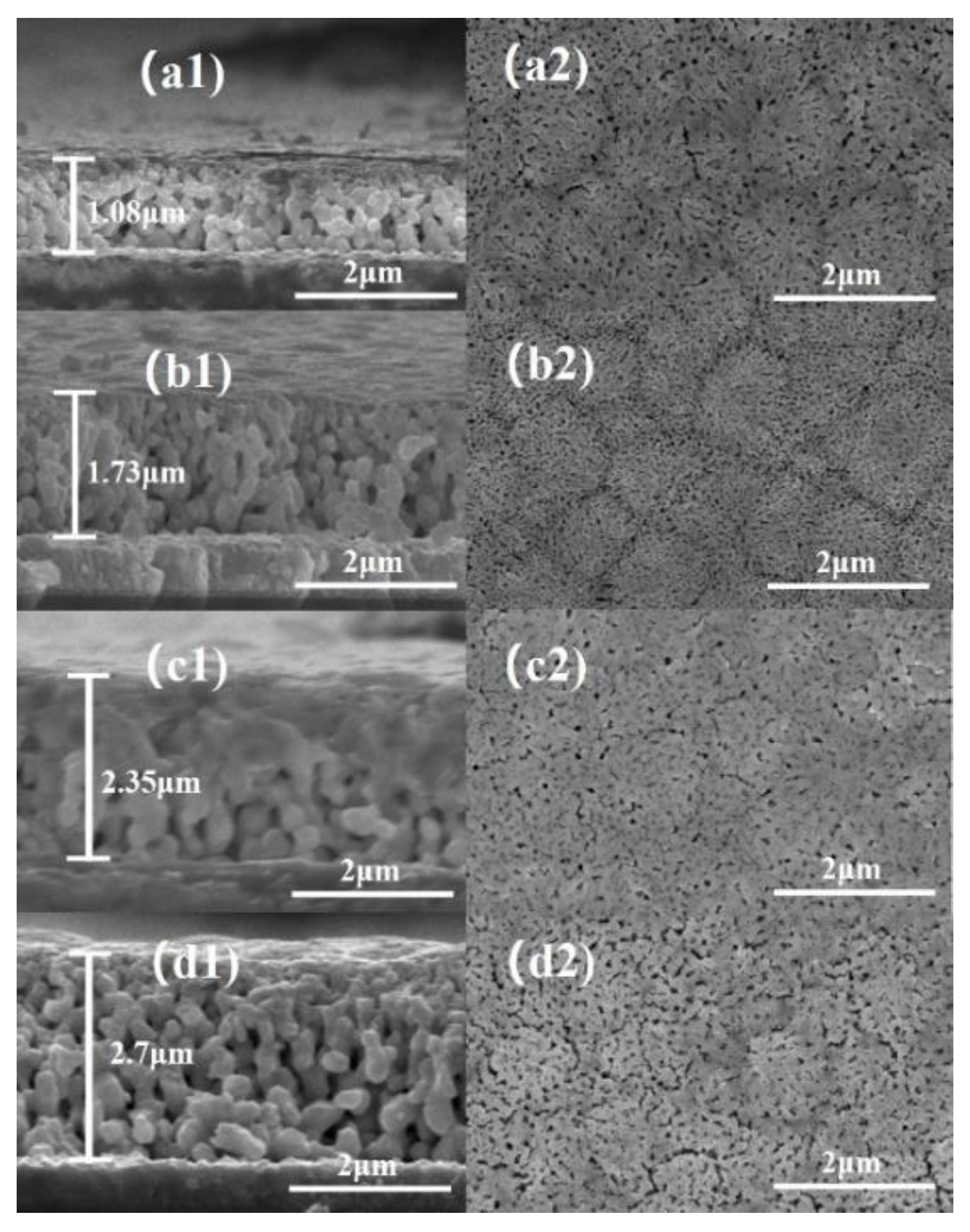
The morphological properties of CdTe thin films were tested by SEM. Figure 1a1–d1 proves that the thicknesses of the CdTe thin films are increased with deposition time, going from approximately 1.08 μm to 2.70 μm. The cross-section morphological images indicate that some islanding are formed and seem to be buried by the high deposition rate, and some restricted particles with definite sizes are also formed and combined to form denser layers.
There are some clusters and porous structures at the surface of the deposited CdTe thin films in Figure 1a2–d2. The composition ratios of deposited CdTe thin films were estimated by EDS measurements, as shown in Table 1.
Even though the CdCl2 annealing treatment can make Te in the film combine with Cd from CdCl2 to form CdTe, the ratios of Cd/Te of all the samples still indicate that Te-rich CdTe thin films were obtained in our work.
3.2. Structural Properties of Deposited CdTe Thin Films
The structural properties of the CdTe films were further investigated by XRD characterizations, as shown in Figure 2a.
By comparison with the standard card (JCPDS 15-0770), it can be seen that the deposited CdTe thin films have diffraction peaks at 2θ = 23.7°, 39.2°, 46.4°, 56.8°, 62.3°, and 71.2°, which correspond to (111), (220), (311), (400), (331), and (422) planes of CdTe, respectively. Comparing with standard PDF card (JCPDS 42-1445), it is speculated that the peaks at 2θ = 26.8°, 33.6°, 38°, 51.8°, and 65° may be caused by substrate SnO2 [19,20]. Peaks at 2θ = 26.8°, 38°, 51.8°, and 65° can also correspond to TeO2 (JCPDS 42-1365). The CdTe thin films deposited with 1.5 h have strong diffraction peaks on (111), (220), and (311) planes. Compared with XRD patterns of CdTe thin films deposited with 1 h, the miscellaneous peaks of the diffraction pattern are significantly reduced, which proves that the quality of the prepared CdTe thin films is improved. The CdTe thin films deposited with 2 h have strong diffraction peaks on the (111), (220), and (311) planes, and the diffraction intensity of the miscellaneous peak is further reduced, which proves that the quality of the prepared CdTe thin films is further improved. The XRD analysis of the thin films deposited with 2.5 h shows that the diffraction peaks of planes (111), (220), and (311) are particularly strong, which perfectly corresponds to the peak positions shown in PDF card (JCPDS 15-0770). According to the Debye Scherrer formula [21]:
where K is the Scherrer constant, λ is the wavelength of X-rays used (λ = 0.15 nm), β is the full-width at half maximum (FWHM) of the diffraction peaks, and θ is Bragg’s angle. The average grain sizes and lattice spacing of (111) plane can be calculated, as shown in Table 1. Compared with the card of PDF (JCPDS 15-0770), it is found that the prepared thin films are of face-centric cubic structure, and the crystalline space group is f-43 m, which is the same as the reported CdTe crystal structure. Raman diffraction patterns of CdTe thin films deposited with different deposition time are shown in Figure 2b. The Raman peaks at the position of 164 cm−1 and 327.5 cm−1 are consistent with the reported Raman peaks of CdTe thin films [22,23]. All the deposited CdTe thin films also have peaks at 139.9 cm−1, which is a combination of TO (CdTe) and elemental Te [24]. It indicates again that Te-rich CdTe thin films have been deposited in our work.
3.3. Optical Properties of Deposited CdTe Thin Films
Figure 3 shows the UV-Vis diffuse-reflection spectra of CdTe thin films with deposition time of 1 h, 1.5 h, 2 h and 2.5 h, respectively. From the images, it can be seen that CdTe thin films have strong absorption of visible light.
And the optical band gaps of the as-deposited thin films were calculated by diffuse-reflection spectra according to the following equation [25]:
In the equation, α was the optical absorption coefficient, hv was the photoelectron energy, Eg was the band gap width, and K was a constant of the material. According to the above equation, CdTe band gaps were calculated as 1.66 eV, 1.48 eV, 1.35 eV, and 1.32 eV, as shown in Figure 3b. The data were consistent with the previous literature reports [12,13].
3.4. Photoelectrochemical Properties of Deposited CdTe Thin Films
AC impedance test was carried out and the results were shown in Figure 4a1–a4.
The test was performed with a three-electrode configuration. Solution resistance Ru between reference electrode and working electrode, double layer capacitance Cd, and charge transfer resistance Rct can be obtained from the test. Rct and Ru of four groups of CdTe thin films in the system were calculated by following formula [26]:
where ω was the frequency, Z’ was the real part of the impedance, Z’’ was the real part of the impedance. As shown in Table 2, the change of Ru is not obvious. Generally speaking, the test solution does not change, nor does Ru. However, there are errors in the measurements, such as the distance between electrodes and the samples in our experiments, the direction of the sample according to the counter electrode, and so on. As deposition time increases, Rct decreases, which may be caused by film thickening and grain size enlargement.
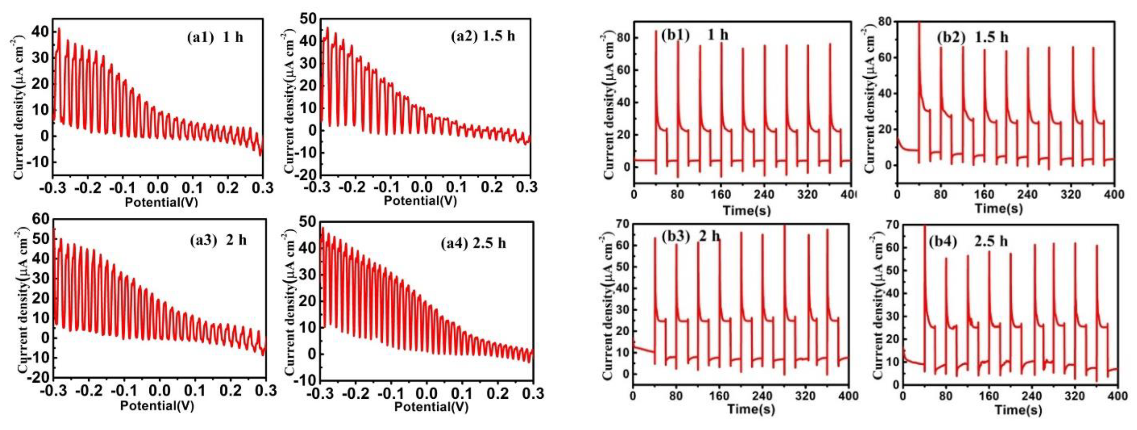
Under chopped AM 1.5 G light illumination (Newport, Oriel Instruments, optical density = 100 mWcm−2), the PEC properties of the films were measured in 0.5 mol/L Na2SO4 solution by an electrochemical work station (CHI 660B). The tests were measured from −0.3 V to 0.3 V and the scanning rate was 0.01 V/s. Finally, the relationship between current and voltage (I–V curves) was presented in Figure 5a.
It can be seen from the I–V curves that the maximum current difference appears at −0.3 V and this potential is negative, which proves that the prepared CdTe film is p-type material. In Figure 5b, with the increase of deposition time, the photocurrent tends to stabilize at around 25 µAcm−2. By comparing the difference of photo and dark current in Table 2, it can be found that the true photo response current first increases and then decreases with the increasing of deposition time. It can be concluded that maximum current can be achieved when the deposition time is 1.5 h and 2 h. The photocurrents are first increased and then decreased, rather than increasing with the deposition time. As known, when the light is irradiated on the semiconductor film, electron and hole pairs are excited inside the semiconductor film. If the film is too thick, the electron–hole pairs will be more likely to recombine before they move to the surface of the films, which will decrease the PEC performance of deposited CdTe thin films [27]. 15 nm CdS film was grown on CdTe film by chemical bath deposition and a 5 nm Pt layer was sputtered on the CdS surface using a sputtering method. The PEC properties of the Pt/CdS/CdTe/FTO structure were characterized, as shown in Figure 6.
The photocurrents are enhanced greatly and the difference of the light-dark current is increased to 240 µAcm−2. The biggest difference of the light–dark current of our deposited CdTe thin film is 20.1 µAcm−2. The difference of the light–dark current is enhanced about 12 times after fabrication of the Pt/CdS/CdTe/FTO structure, which demonstrates that this structure can improve the PEC performance of CdTe thin films greatly.
4. Conclusions
Te-rich CdTe films have been deposited with the electrodeposition method. SEM studies have shown that the film thickness increases with the deposition time, and the deposition time should be controlled at about 1.5 h–2 h to obtain films with good morphology. The annealed CdTe thin films deposited at 1.5 h–2 h have the largest photocurrent and have good PEC performance. The Pt/CdS/CdTe/FTO structure can improve the PEC properties greatly, and the highest photocurrent of 240 µAcm−2 has been achieved.
Author Contributions
Conceptualization, J.L. and X.Z.; methodology, T.M.; software, L.L.; formal analysis, S.W.; investigation, J.Z.; resources, H.S.; data curation, J.H.; writing—original draft preparation, J.L.; writing—review and editing, M.C.; visualization, Y.S.; funding acquisition, L.W. All authors have read and agreed to the published version of the manuscript.
Funding
This research was funded by National Nature Science Foundation of China, grant number 11775139 and 11875186.
Acknowledgments
We acknowledge Instrumental Analysis & Research Center of Shanghai University for the help of characterization works.
Conflicts of Interest
The authors declare no conflict of interest.
References
- Sheridan, M.V.; Hill, D.J.; Sherman, B.D.; Wang, D.; Marquard, S.L.; Wee, K.-R.; Cahoon, J.F.; Meyer, T.J. All-in-One Derivatized Tandem p+n-Silicon-SnO2/TiO2 Water Splitting Photoelectrochemical Cell. Nano Lett. 2017, 17, 2440–2446. [Google Scholar] [CrossRef] [PubMed]
- Su, J.; Minegishi, T.; Katayama, M.; Domen, K. Photoelectrochemical hydrogen evolution from water on a surface modified CdTe thin film electrode under simulated sunlight. J. Mater. Chem. A 2017, 5, 4486–4492. [Google Scholar] [CrossRef]
- Hsiao, K.-J. Energy-band barrier to improve open-circuit voltage of CdTe solar cells. Sol. Energy Mater. Sol. Cells 2014, 120, 647–653. [Google Scholar] [CrossRef]
- Leite, M.S.; Abashin, M.; Lezec, H.J.; Gianfrancesco, A.; Talin, A.A.; Zhitenev, N.B. Nanoscale Imaging of Photocurrent and Efficiency in CdTe Solar Cells. ACS Nano 2014, 8, 11883–11890. [Google Scholar] [CrossRef] [PubMed]
- Major, J.D.; Treharne, R.E.; Phillips, L.J.; DuRose, K. A low-cost non-toxic post-growth activation step for CdTe solar cells. Nature 2014, 511, 334–337. [Google Scholar] [CrossRef]
- Plaza, J.; Martínez, O.; Rubio, S.; Hortelano, V.; Diéguez, E. Growth of CdS and CdTe films by close space vapour sublimation by using SiC resistive elements. CrystEngComm 2013, 15, 2314–2318. [Google Scholar] [CrossRef]
- Islam, M.A.; Huda, Q.; Hossain, M.; Aliyu, M.; Karim, M.; Sopian, K.; Amin, N. High quality 1 μm thick CdTe absorber layers grown by magnetron sputtering for solar cell application. Curr. Appl. Phys. 2013, 13, S115–S121. [Google Scholar] [CrossRef]
- Collins, S.; Vatavu, S.; Evani, V.; Khan, M.; Bakhshi, S.; Palekis, V.; Rotaru, C.; Ferekides, C. Radiative recombination mechanisms in CdTe thin films deposited by elemental vapor transport. Thin Solid Films 2015, 582, 139–145. [Google Scholar] [CrossRef] [Green Version]
- Dharmadasa, I.M.; Echendu, O.; Fauzi, F.; Salim, H.I.; Abdul-Manaf, N.A.; Jasinski, J.B.; Sherehiy, A.; Sumanasekera, G. Study of Fermi level position before and after CdCl2 treatment of CdTe thin films using ultraviolet photoelectron spectroscopy. J. Mater. Sci. Mater. Electron. 2016, 27, 5039–5046. [Google Scholar] [CrossRef] [Green Version]
- Dharmadasa, I.M.; Ojo, A. Unravelling complex nature of CdS/CdTe based thin film solar cells. J. Mater. Sci. Mater. Electron. 2017, 28, 16598–16617. [Google Scholar] [CrossRef] [Green Version]
- Ashead, B.; Khan, S.U. Electrodeposition of Semiconductor n-CdTe and p-CdTe in Aqueous Medium and Aluminum Metal in a Nonaqueous Medium. ECS Trans. 2011, 33, 81–90. [Google Scholar]
- Liyanage, W.P.; Wilson, J.S.; Kinzel, E.C.; Durant, B.; Nath, M. Fabrication of CdTe nanorod arrays over large area through patterned electrodeposition for efficient solar energy conversion. Sol. Energy Mater. Sol. Cells 2015, 133, 260–267. [Google Scholar] [CrossRef]
- Mishra, S.; Nath, M. Growth of vertically aligned CdTe nanorod arrays through patterned electrodeposition. Nano Energy 2013, 2, 1207–1213. [Google Scholar] [CrossRef]
- Liu, Z.-Q.; Xie, X.-H.; Xu, Q.-Z.; Guo, S.-H.; Li, N.; Chen, Y.; Su, Y.-Z. Electrochemical synthesis of ZnO/CdTe core-shell nanotube arrays for enhanced photoelectrochemical properties. Electrochim. Acta 2013, 98, 268–273. [Google Scholar] [CrossRef]
- Ojo, A.; Dharmadasa, I.M. Analysis of electrodeposited CdTe thin films grown using cadmium chloride precursor for applications in solar cells. J. Mater. Sci. Mater. Electron. 2017, 28, 14110–14120. [Google Scholar] [CrossRef] [Green Version]
- Hreid, T.; Tiong, V.T.; Cai, M.; Wang, H.; Will, G. Precisely Controlled Synthesis of High Quality Kesterite Cu2ZnSnS4 Thin Film via Co-Electrodeposited CuZnSn Alloy Film. J. Nanosci. Nanotechnol. 2016, 16, 5701–5706. [Google Scholar] [CrossRef]
- Wang, J.; Li, Q.; Mu, Y.; Li, S.; Yang, L.; Lv, P.; Su, S.; Liu, T.; Su, P.; Yang, H. Fabrication of CdTe thin films grown by the two-step electrodeposition technique on Ni foils. J. Alloy. Compd. 2015, 636, 97–101. [Google Scholar] [CrossRef]
- Jing, J.; Cao, M.; Wu, C.; Huang, J.; Lai, J.; Sun, Y.; Wang, L.; Shen, Y. Chemical bath deposition of SnS nanosheet thin films for FTO/SnS/CdS/Pt photocathode. J. Alloy. Compd. 2017, 726, 720–728. [Google Scholar] [CrossRef]
- Dharmadasa, I.M.; Bingham, P.A.; Echendu, O.; Salim, H.I.; Druffel, T.; Dharmadasa, R.; Sumanasekera, G.U.; Dharmasena, R.R.; Dergacheva, M.; Mit, K.A.; et al. Fabrication of CdS/CdTe-Based Thin Film Solar Cells Using an Electrochemical Technique. Coatings 2014, 4, 380–415. [Google Scholar] [CrossRef]
- Dharmadasa, I.M.; Madugu, M.L.; Olusola, O.I.; Echendu, O.; Fauzi, F.; Diso, D.G.; Weerasinghe, A.R.; Druffel, T.; Dharmadasa, R.; Lavery, B.; et al. Electroplating of CdTe Thin Films from Cadmium Sulphate Precursor and Comparison of Layers Grown by 3-Electrode and 2-Electrode Systems. Coatings 2017, 7, 17. [Google Scholar] [CrossRef] [Green Version]
- El-Sadek, M.A.; Nooralden, A.Y.; Babu, S.M.; Palanisamy, P.; El-Sadek, M.S.A. Influence of different stabilizers on the optical and nonlinear optical properties of CdTe nanoparticles. Opt. Commun. 2011, 284, 2900–2904. [Google Scholar] [CrossRef]
- Dzhagan, V.M.; Lokteva, I.; Himcinschi, C.; Jin, X.; Kolny-Olesiak, J.; Zahn, D.R.T. Phonon Raman spectra of colloidal CdTe nanocrystals: Effect of size, non-stoichiometry and ligand exchange. Nanoscale Res. Lett. 2011, 6, 79. [Google Scholar] [CrossRef] [PubMed] [Green Version]
- Caballero-Briones, F.; Zapata-Navarro, A.; Martel, A.; Iribarren, A.; Peña, J.L.; Castro-Rodríguez, R.; Bartolo-Pérez, P.; Rábago-Bernal, F.; Jiménez-Sandoval, S. Compositional mixture in R.F. sputtered CdTe oxide films. J. Raman Spectrosc. 2003, 16, 38–42. [Google Scholar]
- Dharmadasa, I.M.; Echendu, O.; Fauzi, F.; Abdul-Manaf, N.A.; Olusola, O.I.; Salim, H.I.; Madugu, M.L.; Ojo, A. Improvement of composition of CdTe thin films during heat treatment in the presence of CdCl2. J. Mater. Sci. Mater. Electron. 2016, 28, 2343–2352. [Google Scholar] [CrossRef] [Green Version]
- Kosyachenko, L.; Toyama, T. Current–voltage characteristics and quantum efficiency spectra of efficient thin-film CdS/CdTe solar cells. Sol. Energy Mater. Sol. Cells 2014, 120, 512–520. [Google Scholar] [CrossRef]
- Rizwan, M.; Ahmed, M.U. Electrochemiluminescence study of AuNPs/CdTe-QDs /SWCNTs/chitosan nanocomposite modified carbon nanofiber screen-printed electrode with [Ru(bpy)3]2+/TPrA. Inorg. Chem. Commun. 2019, 106, 54–60. [Google Scholar] [CrossRef]
- Lalitha, S. Characterization of CdTe thin film—Dependence of structural and optical properties on temperature and thickness. Sol. Energy Mater. Sol. Cells 2004, 82, 187–199. [Google Scholar] [CrossRef]
Figure 1.
(a1–d1) Cross-sectional and (a2–d2) top view SEM images of CdTe thin films grown on FTO substrates with deposition times of 1 h, 1.5 h, 2 h, and 2.5 h, respectively.
Figure 1.
(a1–d1) Cross-sectional and (a2–d2) top view SEM images of CdTe thin films grown on FTO substrates with deposition times of 1 h, 1.5 h, 2 h, and 2.5 h, respectively.

Figure 2.
(a) XRD patterns of CdTe thin films with deposition time of 1 h, 1.5 h, 2 h, and 2.5 h, respectively; (b) Raman spectra of CdTe thin films with deposition time of 1 h, 1.5 h, 2 h, and 2.5 h, respectively.
Figure 2.
(a) XRD patterns of CdTe thin films with deposition time of 1 h, 1.5 h, 2 h, and 2.5 h, respectively; (b) Raman spectra of CdTe thin films with deposition time of 1 h, 1.5 h, 2 h, and 2.5 h, respectively.

Figure 3.
(a) UV-Vis diffuse reflection spectra of CdTe thin films with deposition time of 1 h, 1.5 h, 2 h, and 2.5 h, respectively; (b) CdTe band gap patterns with deposition time of 1 h, 1.5 h, 2 h, and 2.5 h, respectively.
Figure 3.
(a) UV-Vis diffuse reflection spectra of CdTe thin films with deposition time of 1 h, 1.5 h, 2 h, and 2.5 h, respectively; (b) CdTe band gap patterns with deposition time of 1 h, 1.5 h, 2 h, and 2.5 h, respectively.

Figure 4.
Impedance test images with deposition time of (a1) 1 h, (a2) 1.5 h, (a3) 2 h, and (a4) 2.5 h, respectively.
Figure 4.
Impedance test images with deposition time of (a1) 1 h, (a2) 1.5 h, (a3) 2 h, and (a4) 2.5 h, respectively.

Figure 5.
(a1–a4) Current-potential curves of CdTe thin films with deposition time of 1 h, 1.5 h, 2 h, and 2.5 h, respectively; (b1–b4) current–time curve of CdTe thin films with deposition time of 1 h, 1.5 h, 2 h, and 2.5 h, respectively.
Figure 5.
(a1–a4) Current-potential curves of CdTe thin films with deposition time of 1 h, 1.5 h, 2 h, and 2.5 h, respectively; (b1–b4) current–time curve of CdTe thin films with deposition time of 1 h, 1.5 h, 2 h, and 2.5 h, respectively.

Figure 6.
(a) Current-potential curves of the Pt/CdS/CdTe/FTO structure; (b) current–time curves of the Pt/CdS/CdTe/FTO structure.
Figure 6.
(a) Current-potential curves of the Pt/CdS/CdTe/FTO structure; (b) current–time curves of the Pt/CdS/CdTe/FTO structure.


Table 1.
The atomic percents determined by EDS, average grain sizes calculated from XRD data, and the band gaps calculated from UV-Vis diffuse-reflection spectra.
Table 1.
The atomic percents determined by EDS, average grain sizes calculated from XRD data, and the band gaps calculated from UV-Vis diffuse-reflection spectra.
| Deposition Time (h) | The Atomic Percent of Cd:Te (%) | Lattice Spacing (nm) | Lattice Parameter (nm) | Average Grain Size (nm) | Band Gap (eV) |
|---|---|---|---|---|---|
| 1 | (46.67 ± 0.51) : (53.33 ± 0.51) | 0.3681 ± 0.0002 | 0.6375 ± 0.0002 | 30.9 ± 0.1 | 1.66 ± 0.02 |
| 1.5 | (47.63 ± 0.51) : (52.37 ± 0.51) | 0.3732 ± 0.0002 | 0.6465 ± 0.0002 | 36.5 ± 0.1 | 1.48 ± 0.02 |
| 2 | (47.85 ± 0.51) : (52.15 ± 0.51) | 0.3745 ± 0.0002 | 0.6486 ± 0.0002 | 40.1 ± 0.1 | 1.35 ± 0.02 |
| 2.5 | (49.33 ± 0.51) : (50.67 ± 0.51) | 0.3751 ± 0.0002 | 0.6497 ± 0.0002 | 40.1 ± 0.1 | 1.32 ± 0.02 |
Table 2.
Measured AC impedance data and photocurrent data of CdTe prepared at different deposition time.
Table 2.
Measured AC impedance data and photocurrent data of CdTe prepared at different deposition time.
| Deposition Time (h) | Ru (Ω) | Rct (Ω) | Photocurrent (μAcm−2) | Dark Current (μAcm−2) | Difference (μAcm−2) |
|---|---|---|---|---|---|
| 1 | 23.2 ± 0.2 | 56.3 ± 0.1 | 22.0 ± 0.1 | 4.0 ± 0.1 | 18.0 ± 0.1 |
| 1.5 | 21.3 ± 0.2 | 36.7 ± 0.1 | 24.9 ± 0.1 | 4.8 ± 0.1 | 20.1 ± 0.1 |
| 2 | 23.8 ± 0.2 | 17.8 ± 0.1 | 24.7 ± 0.1 | 7.4 ± 0.1 | 17.3 ± 0.1 |
| 2.5 | 20.1 ± 0.2 | 16.2 ± 0.1 | 25.2 ± 0.1 | 8.9 ± 0.1 | 16.3 ± 0.1 |
© 2020 by the authors. Licensee MDPI, Basel, Switzerland. This article is an open access article distributed under the terms and conditions of the Creative Commons Attribution (CC BY) license (http://creativecommons.org/licenses/by/4.0/).
Share and Cite
MDPI and ACS Style
Ling, J.; Zhang, X.; Mao, T.; Li, L.; Wang, S.; Cao, M.; Zhang, J.; Shi, H.; Huang, J.; Shen, Y.; et al. Electrodeposition of CdTe Thin Films for Solar Energy Water Splitting. Materials 2020, 13, 1536. https://doi.org/10.3390/ma13071536
AMA Style
Ling J, Zhang X, Mao T, Li L, Wang S, Cao M, Zhang J, Shi H, Huang J, Shen Y, et al. Electrodeposition of CdTe Thin Films for Solar Energy Water Splitting. Materials. 2020; 13(7):1536. https://doi.org/10.3390/ma13071536
Chicago/Turabian StyleLing, Jun, Xulei Zhang, Ting Mao, Lei Li, Shilin Wang, Meng Cao, Jijun Zhang, Haozhi Shi, Jian Huang, Yue Shen, and et al. 2020. "Electrodeposition of CdTe Thin Films for Solar Energy Water Splitting" Materials 13, no. 7: 1536. https://doi.org/10.3390/ma13071536
Note that from the first issue of 2016, this journal uses article numbers instead of page numbers. See further details here.