CuPc: Effects of its Doping and a Study of Its Organic-Semiconducting Properties for Application in Flexible Devices

Abstract
:
1. Introduction
2. Materials and Methods
2.1. General Remarks
2.2. Thin Film Deposition and Characterization
2.3. Theoretical Method
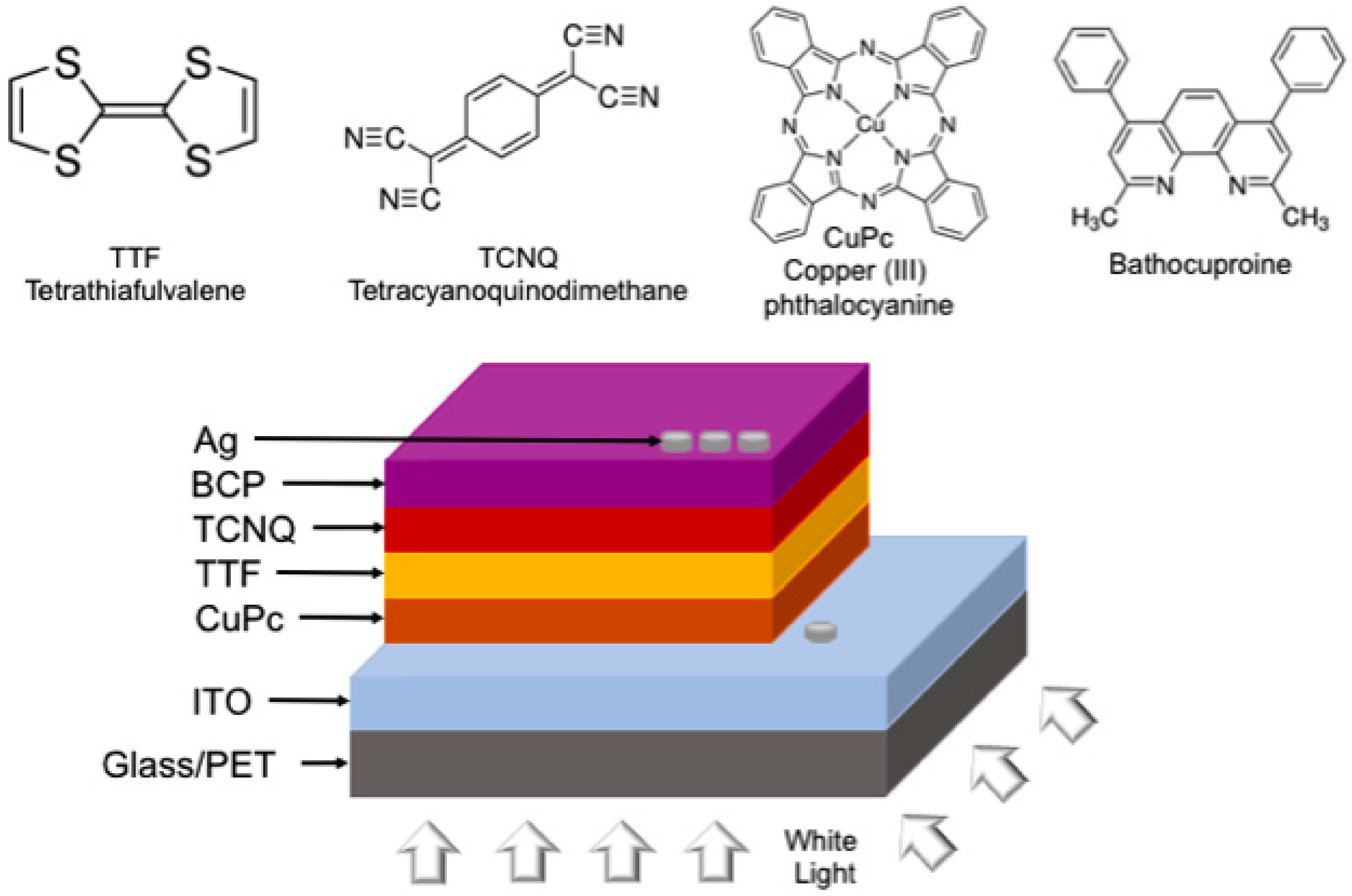
2.4. Devices Assembly and Characterization
3. Results and Discussion
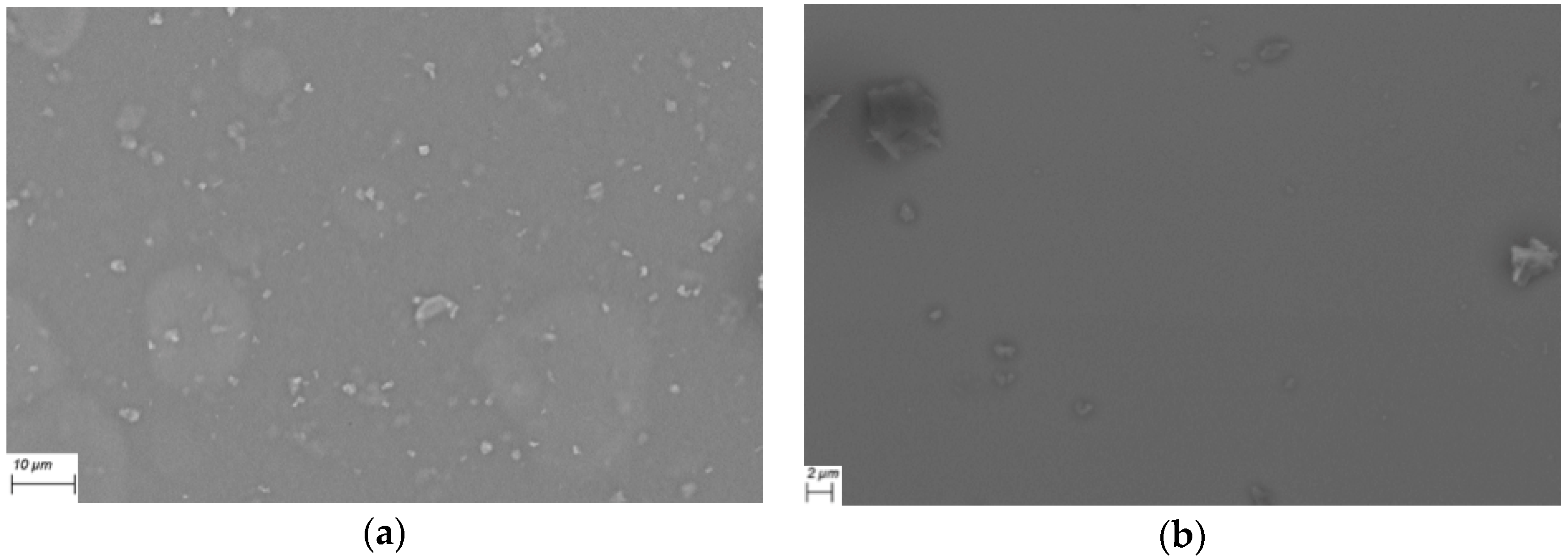
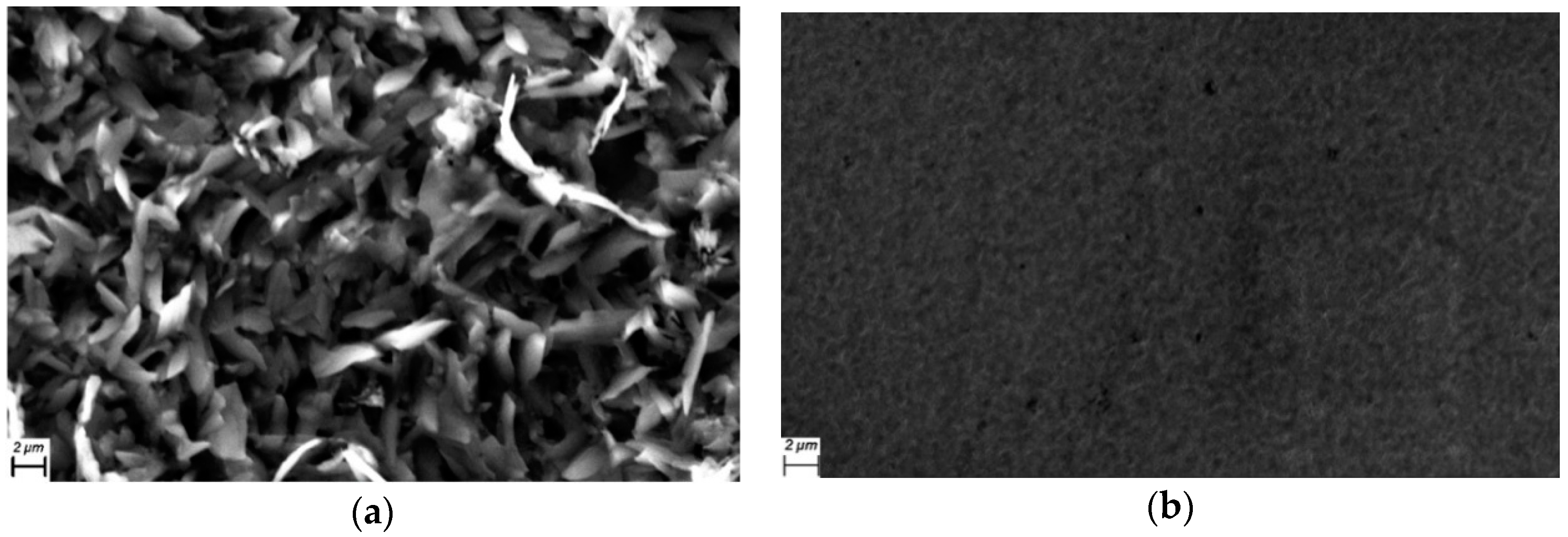
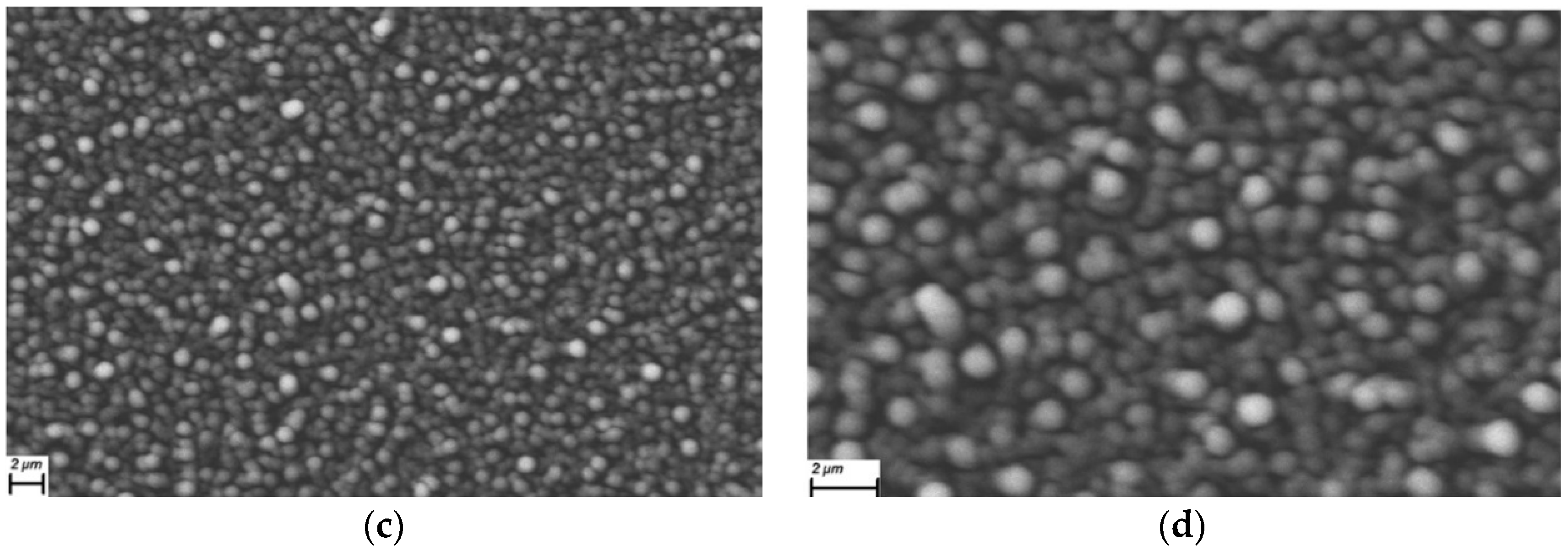
3.1. Thin Film Structure and Morphology
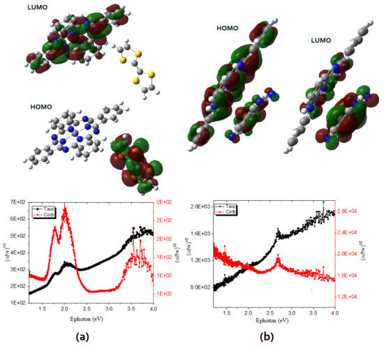
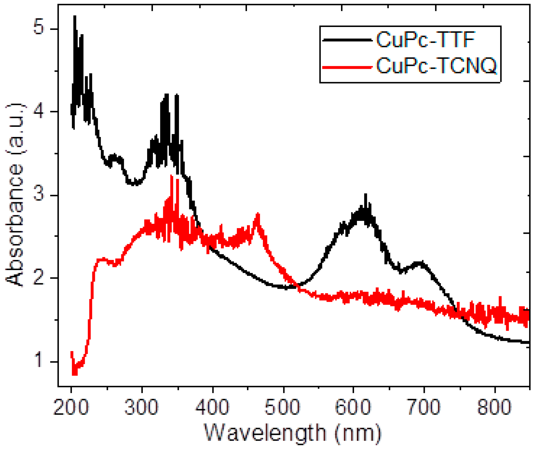
3.2. Thin Film Optical and Electrical Characterization
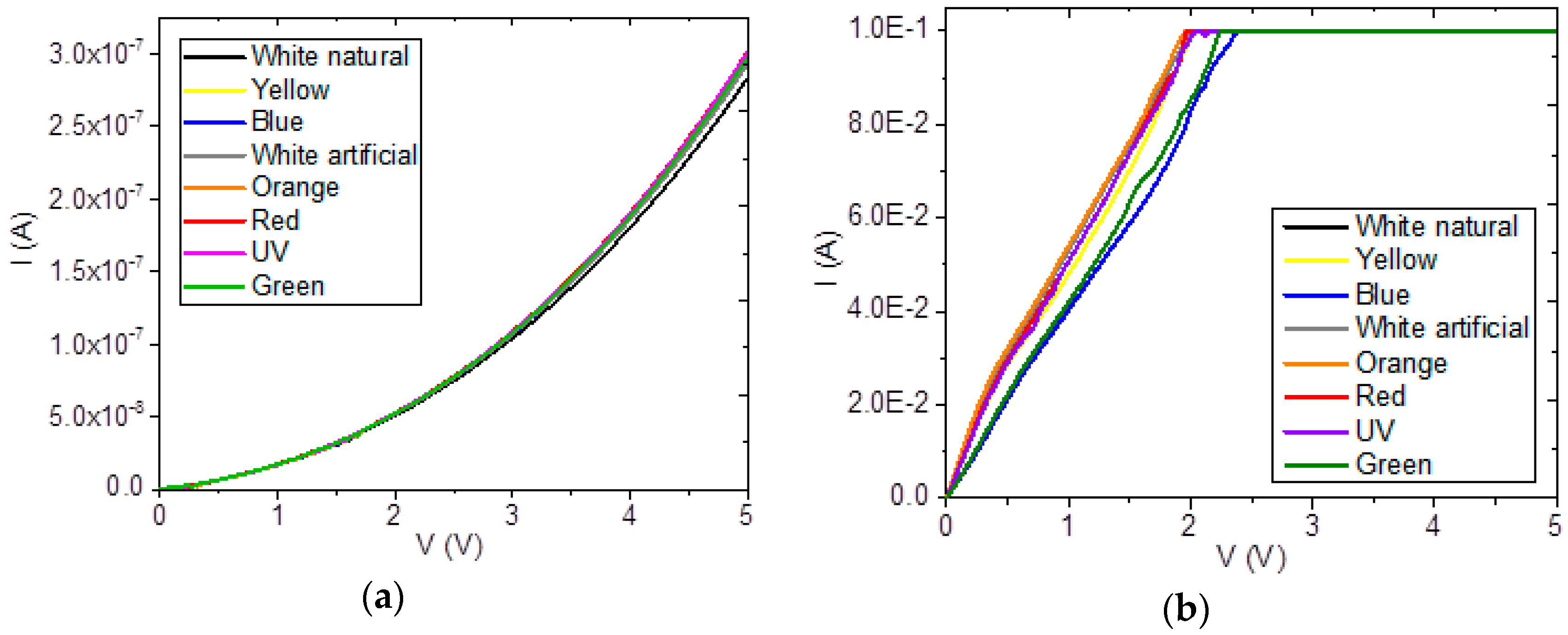
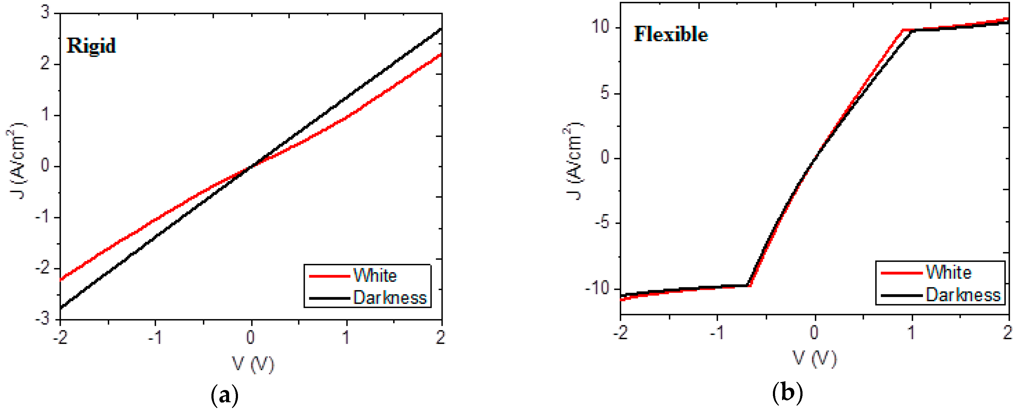
3.3. Electric Characterization of Heterojunction Planar Devices
4. Conclusions and Further Work
Author Contributions
Funding
Acknowledgments
Conflicts of Interest
References
- Hall, B.H.; Helmers, C. The Role of Patent Protection in (Clean/Green) Technology Transfer. Natl. Bureau Econ. Res. 2010. [Google Scholar] [CrossRef]
- OECD. Fostering Innovation for Green Growth. In OECD Green Growth Studies; OECD Publishing: Paris, France, 2017. [Google Scholar] [CrossRef]
- Dong, X.; Luo, G.; Cai, Y.; Gao, W. A bibliometric analysis of solar power research from 1991 to 2010. Scientometrics 2012, 93, 1101–1117. [Google Scholar] [CrossRef]
- Serrano, E.; Rus, G.; Garcia-Martinez, J. Nanotechnology for sustainable energy. Renew. Sustain. Energy Rev. 2009, 13, 2373–2384. [Google Scholar] [CrossRef]
- Schaeffer, R.; Szklo, A.; Lucena, A.F.P.; Viviescas, C.; Lima, L.; Nascimiento, G.; Ludovique, C.; Amendola, F.; Magalar, L.; Huback, V.; et al. Contribución de las Energías Renovables Variables a la Seguridad Energética en América Latina; BID, Banco Interamericano de Desarrollo: América Latina, 2017; pp. 13–15. [Google Scholar]
- BID, Banco Interamericano de Desarrollo. Available online: https://www.iadb.org/en/news/news-releases/2014-10-28/climatescope-2014%2C10962.html (accessed on 28 September 2018).
- Zhao, H.; He, Z.; Zhang, X.; Zhang, Z.; Diyaf, A.; Lind, A.H.N.; Liang, C.; Wilson, J.I.B. A preliminary investigation into hybrid photovoltaic cells with organic phthalocyanines and amorphous silicon heterojunction. J. Phys. D Appl. Phys. 2015, 48, 195102. [Google Scholar] [CrossRef]
- Schock, H.W. Thin Film Photovoltaic. Appl. Surf. Sci. 1996, 92, 606–616. [Google Scholar] [CrossRef]
- Green, M.A.; Emery, K.; Hishikawa, Y.; Warta, W.; Dunlop, E.D. Solar cell efficiency tables (version 46). Prog. Photovolt. Res. Appl. 2015, 23, 805–812. [Google Scholar] [CrossRef] [Green Version]
- Hains, A.W.; Liang, Z.; Woodhouse, M.A.; Gregg, B.A. Molecular Semiconductors in Organic Photovoltaic Cells. Chem. Rev. 2010, 110, 6689–6735. [Google Scholar] [CrossRef]
- Leznoff, C.C.; Lever, A.B.P. Phthalocyanines: Properties and Applications; VCH: Weinheim, Germany, 1997; Volume 1–4, pp. 1–1568. ISBN 978-0-471-23899-7. [Google Scholar]
- Anastas, P.T.; Zimmerman, J.B. Peer reviewed: Design through the 12 principles of green engineering. Environ. Sci. Technol. 2003, 37, 94A–101A. [Google Scholar] [CrossRef]
- Rodríguez Morgade, M.S.; De la Torre, G.; Torres, T. Design and Synthesis of Low-Symmetry Phthalocyanines and Related Systems. In The Porphyrin Handbook, 1st ed.; Kadish, K.M., Smith, K.M., Guilard, R., Eds.; Academic Press: San Diego, CA, USA, 2003; Volume 15, pp. 125–160. ISBN 0-12-393225-4. [Google Scholar]
- Metz, J.; Hanack, M. Synthesis, Characterization and Conductivity or (μ-Cyano)(phthalocyaninato)cobalt(III). J. Am. Chem. Soc. 1983, 105, 828–830. [Google Scholar] [CrossRef]
- Seoudi, R.; El-Bahy, G.S.; El Sayed, Z.A. FTIR, TGA and DC electrical conductivity studies of phthalocyanine and its complexes. J. Mol. Struct. 2005, 753, 119–126. [Google Scholar] [CrossRef]
- Cyhan, T.; Altindal, A.; Erbil, M.K.; Bekaroğlu, Ö. Synthesis, characterization, conduction and gas sensing properties of novel multinueclar metallo phthalocyanines (Zn, Co) with alkylthio substituents. Polyhedron 2006, 25, 737–746. [Google Scholar] [CrossRef]
- Morales-Saavedra, O.G.; Sánchez-Vergara, M.E.; Rodríguez-Rosales, A.A.; Ortega-Martínez, R.; Ortiz-Rebollo, A.; Frontana-Uribe, B.A.; García-Montalvo, V. Synthesis and electrical, spectroscopic and nonlinear optical properties of cobalt molecular materials obtained from PcCo(CN)L (L = ethylenediamine, 1,4-diaminebutane, 1,12-diaminododecane and 2,6-diamineanthraquinone). Mater. Chem. Phys. 2010, 123, 776–785. [Google Scholar] [CrossRef]
- Sánchez-Vergara, M.E.; García-Montalvo, V.; Santoyo-Salazar, J.; Fragoso-Soriano, R.J.; Jiménez-Sandoval, O. Synthesis and characterization of NiPcTSTNa(L) thin films. Bull. Mater. Sci. 2012, 35, 759–766. [Google Scholar] [CrossRef]
- Hamui, L.; Sánchez-Vergara, M.E.; Sánchez-Ruiz, R.; Ruanova-Ferreiro, D.; Ballinas-Indili, R.; Álvarez-Toledano, C. New Development of Membrane Base Optoelectronic Devices. Polymers 2018, 10, 16. [Google Scholar] [CrossRef]
- Basova, T.; Hassan, A.; Durmuſ, M.; Gürek, A.G.; Ahsen, V. Liquid crystalline metal phthalocyanines: Structural organization on the substrate surface. Coord. Chem. Rev. 2016, 310, 131–153. [Google Scholar] [CrossRef]
- Fernández-Ariza, J.; Krick Calderón, R.M.; Rodríguez-Morgade, M.S.; Guldi, R.M.; Torres, T. Phthalocyanine−Perylenediimide Cart Wheels. J. Am. Chem. Soc. 2016, 138, 12963–12974. [Google Scholar] [CrossRef]
- El-Nahass, M.M.; Zeyada, H.M.; Aziz, M.S.; El-Ghamaz, N.A. Structural and optical properties of thermally evaporated zinc phthalocyanine thin films. Opt. Mater. 2004, 27, 491–498. [Google Scholar] [CrossRef]
- Chaidogiannos, G.; Petraki, F.; Glezos, N.; Kennou, S.; Nešpurek, S. Low voltage operating OFETs based on solution-processed metal phthalocyanines. Appl. Phys. A 2009, 96, 763–767. [Google Scholar] [CrossRef]
- Wang, J.B.; Li, W.L.; Chu, B.; Lee, C.S.; Su, Z.S.; Zhang, G.; Wu, S.H.; Yan, F. High speed responsive near infrared photodetector focusing on 808 nm radiation using hexadecafluoro-copper-phthalocyanine as the acceptor. Org. Electron. Phys. Mater. Appl. 2011, 12, 34–38. [Google Scholar] [CrossRef]
- Zhang, J.; Gu, P.; Long, G.; Ganguly, R.; Li, Y.; Aranti, N.; Yamadac, H.; Zhang, Q. Switching charge-transfer characteristics from ptype to n-type through molecular “doping” (cocrystallization). Chem. Sci. 2016, 7, 3851–3856. [Google Scholar] [CrossRef]
- Bendikov, M.; Wudl, F.; Perepichka, D.F. Tetrathiafulvalenes, oligoacenenes, and their buckministerfullerene derivatives: The brick and mortar of organic electronics. Chem. Rev. 2004, 104, 4891–4945. [Google Scholar] [CrossRef] [PubMed]
- Xie, M.; Zhang, S.; Cai, B.; Zou, Y.; Zeng, H. N- and p-type doping of antimonene. RSC Adv. 2016, 6, 14620–14625. [Google Scholar] [CrossRef]
- Más-Montoya, M. Synthesis of Novel Heteroacene Systems and Study of Its Properties as Organic Semiconductors for Molecular Electronic Applications. Ph.D. Thesis, Faculty of Chemistry, University of Murcia, Murcia, Spain, 2015. [Google Scholar]
- Becke, A.D. Density functional exchange-energy approximation with correct asymptotic behavior. Phys. Rev. A 1988, 38, 3098–3100. [Google Scholar] [CrossRef]
- Perdew, J.P.; Wang, Y. Accurate and simple analytic representation of the electron-gas correlation energy. Phys. Rev. B 1992, 45, 13244–13249. [Google Scholar] [CrossRef]
- Frisch, M.J.; Trucks, G.W.; Schlegel, H.B.; Scuseria, G.E.; Robb, M.A.; Cheeseman, J.R.; Scalmani, G.; Barone, V.; Mennucci, B.; Petersson, G.A.; et al. Gaussian 09, Revision A.01; Gaussian, Inc.: Wallingford, CT, USA, 2009. [Google Scholar]
- Touka, N.; Benelmadjat, H.; Boudine, B.; Halimi, O.; Sebais, M. Copper phthalocyanine nanocrystals embedded into polymer host: Preparation and structural characterization. J. Assoc. Arab Univ. Basic Appl. Sci. 2013, 13, 52–56. [Google Scholar] [CrossRef]
- El-Nahass, M.M.; Abd-El-Rahman, K.F.; Al-Ghamdi, A.A.; Asiri, A.M. Optical properties of thermally evaporated tin-phthalocyanine dichloride thin films, SnPcCl2. Phys. B Condens. Matter 2004, 344, 398–406. [Google Scholar] [CrossRef]
- Hart, M.M. Cationic Exchange Reactions Involving Dilithium Phthalocyanine. Master’s Thesis, Wright State University, Dayton, OH, USA, 11 December 2009. [Google Scholar]
- Young-Inn, K.; Chan-Kyou, J.; Yong-Min, L.; Sung-Nak, C. Synthesis and Characterization of Tetrathiafulvalene (TTF) and 7,7,8,8-Tetracyanoquinodimethane (TCNQ) Compounds with PdX2 (X = Cl, NO3 and Hexafluoroacetylacetonate). Bull. Korean Chem. Soc. 2002, 23, 1754–1758. [Google Scholar] [CrossRef]
- Galfo, L.; Cordeiro, M.R.; Freitas, A.R.; Moreira, W.C.; Girotto, E.M.; Zucolotto, V. The effects of temperature on the molecular orientation of zinc phthalocyanine films. J. Mater. Sci. 2010, 45, 1366–1370. [Google Scholar] [CrossRef]
- El-Nahass, M.M.; Ammar, A.H.; Farag, A.A.M.; Atta, A.A.; El-Zaidia, E.F.M. Effect of heat treatment on morphological, structural and optical properties of CoMTPP thin films. Solid State Sci. 2011, 13, 596–600. [Google Scholar] [CrossRef]
- Vasseur, K.; Rand, B.P.; Cheyns, D.; Froyen, L.; Heremans, P. Structural Evolution of Evaporated Lead Phthalocyanine Thin Films for Near-Infrared Sensitive Solar Cells. Chem. Mater. 2011, 23, 886–895. [Google Scholar] [CrossRef]
- Della Pirriera, M.; Puigdollers, J.; Voz, C.; Stella, M.; Bertomeu, J.; Alcubilla, R. Optoelectronic properties of CuPc thin films deposited at different substrate temperatures. J. Phys. D Appl. Phys. 2009, 42, 145102. [Google Scholar] [CrossRef] [Green Version]
- Socol, M.; Preda, N.; Rasoga, O.; Breazu, C.; Stavarache, I.; Stanculescu, F.; Socol, G.; Gherendi, F.; Grumezescu, V.; Popescu-Pelin, G.; et al. Flexible heterostructures based on metal phthalocyanines thin films obtained by MAPLE. Appl. Surf. Sci. 2016, 374, 403–410. [Google Scholar] [CrossRef] [Green Version]
- Regimol, C.C.; Menon, C.S. Effect of annealing and γ irradiation on tin phthalocyanine thin films. Mater. Sci. Pol. 2007, 25, 649–655. [Google Scholar]
- Novotny, M.; Bulir, J.; Bensalah-Ledoux, A.; Guy, S.; Fitl, P.; Vrnata, M.; Lancok, J.; Moine, B. Optical properties of zinc phthalocyanine thin films prepared by pulsed laser deposition. Appl. Phys. A 2014, 117, 377–381. [Google Scholar] [CrossRef]
- Tauc, J. Optical properties and electronic structure of amorphous Ge and Si. Mater. Res. Bull. 1968, 3, 37–46. [Google Scholar] [CrossRef]
- Mok, T.M.; O’Leary, S.K. The dependence of the Tauc and Cody optical gaps associated with hydrogenated amorphous silicon on the film thickness: αlαl Experimental limitations and the impact of curvature in the Tauc and Cody plots. J. Appl. Phys. 2007, 102, 113525-1–113525-9. [Google Scholar] [CrossRef]
- Fox, M. Optical Properties of Solids, 1st ed.; Oxford University Press: New York, NY, USA, 2001; pp. 51–73, 165–183. ISBN 978-0-19-850612-6. [Google Scholar]
- Cody, G.D.; Brooks, B.G.; Abeles, B. Optical absorption above the optical gap of amorphous silicon hydride. Sol. Energy Mater. 1982, 8, 231–240. [Google Scholar] [CrossRef]
- García-Moreno, G. Semiconductores Orgánicos Pi-Conjugados Basados en Tiofeno. Un Studio Teórico. Ph.D. Thesis, Faculty of Experimental Science, University of Jaén, Jaén, Spain, 1 May 2012. [Google Scholar]
- Sánchez-Vergara, M.E.; Leyva-Esqueda, M.; Alvárez-Bada, J.R.; García-Montalvo, V.; Rojas-Montoya, I.D.; Jiménez-Sandoval, O. Optical and Electrical Properties of TTF-MPcs (M = Cu, Zn) Interfaces for Optoelectronic Applications. Molecules 2015, 20, 21037–21049. [Google Scholar] [CrossRef] [Green Version]
- Poray-Koshits, E.A. Submikroskopische Struktur einiger komplexer Gläser. Glastechn. Ber. 1959, 34, 450–459. [Google Scholar]
- Vogel, W. Neue Erkenntnisse über die Glasstruktur. Silikattech 1959, 10, 241–250. [Google Scholar]
- Vogel, W. Struktur und Kristallisation der Gläser, 1st ed.; VEB Deutscher Verlag für Grundstoffindustrie: Leipzig, Germany, 1965. [Google Scholar]
- Sharples, A. Introduction to Polymer Crystallization, 1st ed.; Edward Arnold Ltd.: London, UK, 1966. [Google Scholar]
- Pérez-Cárdenas, F.; Del Castillo, L.F.; Vera-Graziano, R. Modified avrami expression for polymer crystallization kinetics. J. Appl. Polym. Sci. 1991, 43, 779–782. [Google Scholar] [CrossRef]
- Hassan, A.K.; Gould, R.D. The interpretation of current density-voltage and activation energy measurements on freshly prepared and heat-treated nickel phthalocyanine thin films. Int. J. Electron. 1993, 74, 59–65. [Google Scholar] [CrossRef]
- Gravano, S.; Hassan, A.K.; Gould, R.D. Effects of annealing on the trap distribution of cobalt phthalocyanine thin films. Int. J. Electron. 1991, 70, 477–484. [Google Scholar] [CrossRef]
- Anthopoulos, T.D.; Shafai, T.S. SCLC Measurements in Nickel Phthalocyanine Thin Films. Phys. Status Solidi A 2000, 181, 569–574. [Google Scholar] [CrossRef]
- Herrera Martín, E. Diseño, Síntesis y Estudio de Nuevos Semiconductores Orgánicos para la Fabricación de Transistores de Efecto Campo. Ph.D. Thesis, School of Chemical Sciences, Universidad Complutense de Madrid, Madrid, Spain, 2013. [Google Scholar]
- Gould, R.D. DC electrical measurements on evaporated thin films of copper phthalocyanine. Thin Solid Films 1985, 125, 63–69. [Google Scholar] [CrossRef]
- Gould, R.D. Structure and electrical conduction properties of phthalocyanine thin films. Coord. Chem. Rev. 1996, 156, 237–274. [Google Scholar] [CrossRef]
- Allara, D.L.; Bässler, H.; Echegoyen, L.; Kagan, C.R.; Köhler, A.; Maitani, M.M.; Pinzón, J.R.; Saito, G.; Schlenker, C.W.; Szulczewski, G.; et al. Unimolecular and Supramolecular Electronics I, Chemistry and Physics Meet at Metal-Molecule Interfaces; Metzger, R.M., Ed.; Springer: Berlin/Heidelberg, Germany, 2012; Chapter 218; Volume 312, pp. 1–65. [Google Scholar]


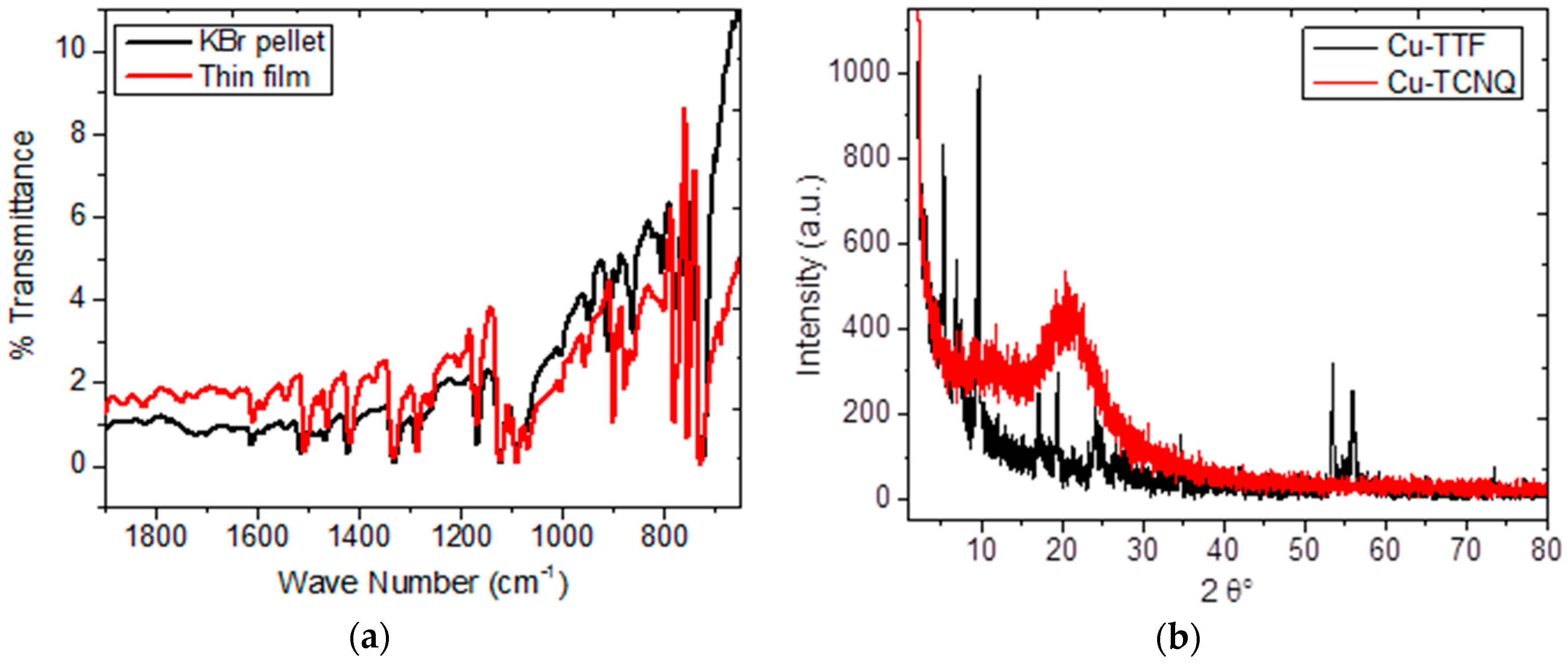
| Sample | CuPc ν(C=N) cm−1 | CuPc ν(C–H) cm−1 | CuPc ν(C=C) cm−1 | TTF ν(C=C) cm−1 | TTF ν(C–S) cm−1 | TCNQ ν(C=C–H) cm−1 | TCNQ ν(C=C) cm−1 |
|---|---|---|---|---|---|---|---|
| CuPc-TTF (KBr pellet) | 1479, 1334 | 1164, 1121, 780, 752 | 1610, 1101 | 1089 | 846, 781 | - | - |
| CuPc-TTF (film) | 1484, 1335 | 1167, 1121, 778, 751 | 1597, 1094 | 1081 | 844, 780 | - | - |
| CuPc-TCNQ (KBr pellet) | 1483, 1333 | 1167, 1115, 774, 752 | 1609, 1100 | - | - | 1203 | 1610 |
| CuPc-TCNQ (film) | 1481, 1332 | 1165, 1120, 772, 750 | 1610, 1093 | - | - | 1206 | 1610 |
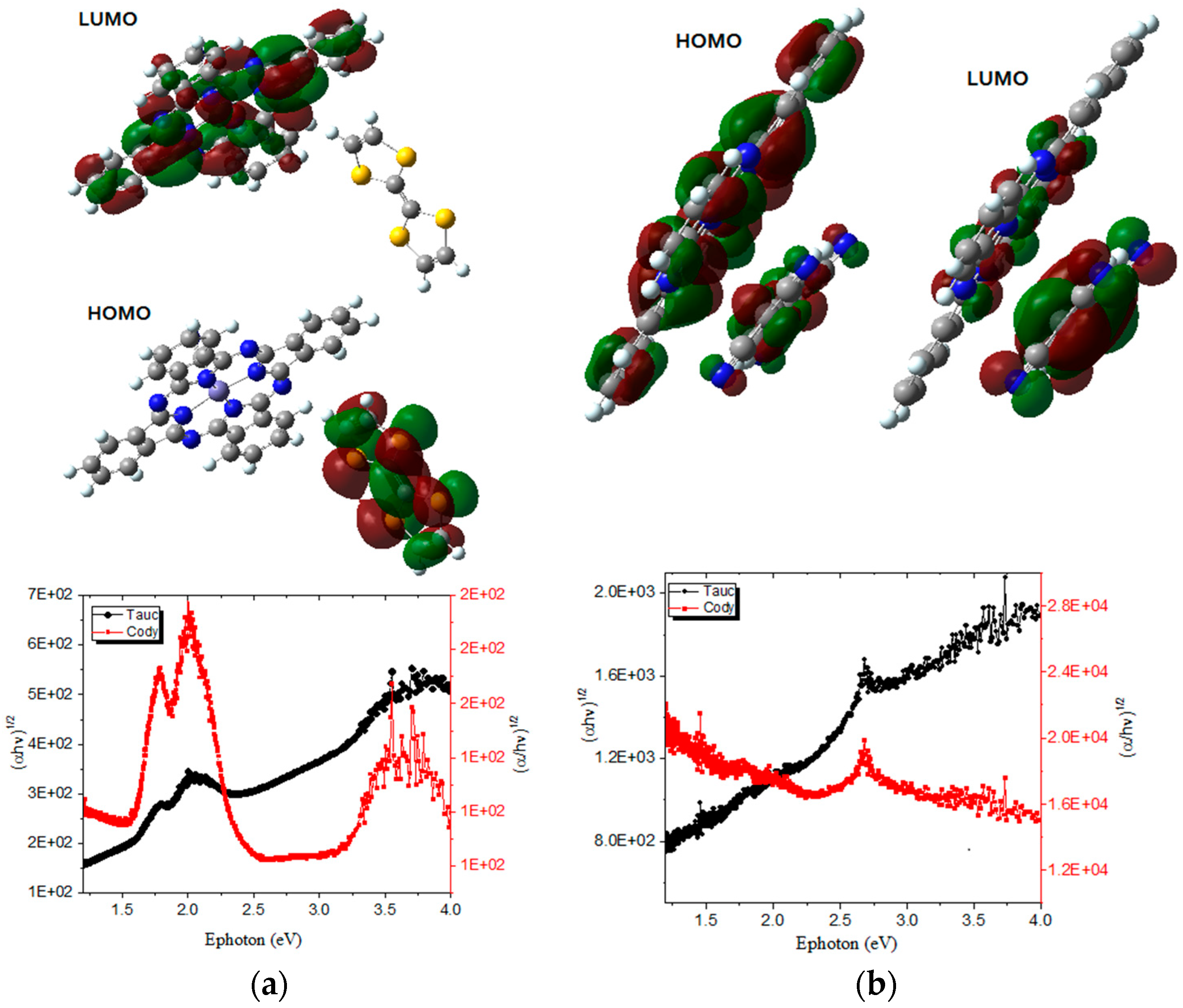
| Sample | Tauc Direct Bandgap (eV) | Tauc Indirect Bandgap (eV) | Cody Direct Bandgap (eV) | Cody Indirect Bandgap (eV) | DFT Bandgap (eV) |
|---|---|---|---|---|---|
| CuPc-TTF | 1.1 | 1.4 | 1.7 | 1.6 | 2.59 |
| CuPc-TCNQ | 2.2 | 1.9 | 2.3 | 2.2 | 2.73 |
| Parameters, Darkness | Parameters, Illuminated | ||||
|---|---|---|---|---|---|
| μ (glass) | 1.59 × 10⁻⁹ | (cm2)/V·s | μ (glass) | 3.94 × 10⁻¹⁰ | (cm2)/V·s |
| p0 (glass) | 7.74 × 10²³ | m−3 | p0 (glass) | 7.74 × 10²³ | m−3 |
| P0 (glass) | - | 1/(J·m3) | P0 (glass) | - | 1/(J·m3) |
| Nte (glass) | - | 1/m3 | Nte (glass) | - | 1/m3 |
| μ (PET) | 1.84 × 10⁻⁹ | (cm2)/V s | μ (PET) | 4.51 × 10⁻⁹ | (cm2)/V s |
| p0 (PET) | 7.74 × 10²³ | m−3 | p0 (PET) | 7.74 × 10²³ | m−3 |
| P0 (PET) | 5.58 × 1043 | 1/(J·m3) | P0 (PET) | 6.05 × 1043 | 1/(J·m3) |
| Nte (PET) | 1.22 × 1024 | 1/m3 | Nte (PET) | 1.25 × 1024 | 1/m3 |
© 2019 by the authors. Licensee MDPI, Basel, Switzerland. This article is an open access article distributed under the terms and conditions of the Creative Commons Attribution (CC BY) license (http://creativecommons.org/licenses/by/4.0/).
Share and Cite
Leyva Esqueda, M.; Sánchez Vergara, M.E.; Álvarez Bada, J.R.; Salcedo, R. CuPc: Effects of its Doping and a Study of Its Organic-Semiconducting Properties for Application in Flexible Devices. Materials 2019, 12, 434. https://doi.org/10.3390/ma12030434
Leyva Esqueda M, Sánchez Vergara ME, Álvarez Bada JR, Salcedo R. CuPc: Effects of its Doping and a Study of Its Organic-Semiconducting Properties for Application in Flexible Devices. Materials. 2019; 12(3):434. https://doi.org/10.3390/ma12030434
Chicago/Turabian StyleLeyva Esqueda, Mariel, María Elena Sánchez Vergara, José Ramón Álvarez Bada, and Roberto Salcedo. 2019. "CuPc: Effects of its Doping and a Study of Its Organic-Semiconducting Properties for Application in Flexible Devices" Materials 12, no. 3: 434. https://doi.org/10.3390/ma12030434