Communication

Effect of Simultaneous Mechanical and Electrical Stress on the Electrical Performance of Flexible In-Ga-Zn-O Thin-Film Transistors

1
School of Electrical Engineering, Kookmin University, Seoul 02707, Korea
2
School of Electrical and Electronics Engineering, Chung-Ang University, Seoul 06974, Korea
3
School of Information Science and Engineering, Shenyang University of Technology, Shenyang 110870, China
*
Authors to whom correspondence should be addressed.
Materials 2019, 12(19), 3248; https://doi.org/10.3390/ma12193248
Submission received: 11 September 2019 / Revised: 27 September 2019 / Accepted: 2 October 2019 / Published: 4 October 2019
(This article belongs to the Section Electronic Materials)

Abstract

:
We investigated the effect of simultaneous mechanical and electrical stress on the electrical characteristics of flexible indium-gallium-zinc oxide (IGZO) thin-film transistors (TFTs). The IGZO TFTs exhibited a threshold voltage shift (∆VTH) under an application of positive-bias-stress (PBS), with a turnaround behavior from the positive ∆VTH to the negative ∆VTH with an increase in the PBS application time, whether a mechanical stress is applied or not. However, the magnitudes of PBS-induced ∆VTH in both the positive and negative directions exhibited significantly larger values when a flexible IGZO TFT was under mechanical-bending stress than when it was at the flat state. The observed phenomena were possibly attributed to the mechanical stress-induced interface trap generation and the enhanced hydrogen diffusion from atomic layer deposition-grown Al2O3 to IGZO under mechanical-bending stress during PBS. The subgap density of states was extracted before and after an application of PBS under both mechanical stress conditions. The obtained results in this study provided potent evidence supporting the mechanism suggested to explain the PBS-induced larger ∆VTHs in both directions under mechanical-bending stress.

1. Introduction

Indium-gallium-zinc oxide (IGZO) thin-film transistor (TFT) is being widely used for the backplane of large-area active-matrix organic-light-emitting diode displays, owing to its excellent properties including high field-effect mobility (μFE), low-off current, high uniformity, and low process temperature [1,2,3,4,5,6,7,8,9,10,11]. Recently, there is increasing interest in the application of IGZO TFTs in demonstrating the active-matrix backplane for flexible displays [12,13,14,15,16]. Flexible displays have many advantages over conventional glass substrate-based displays including better durability, lighter weight, and thinner dimension. In addition, flexible displays can enable a lot of new applications because of their ability to have unique curved shapes.
Nevertheless, there are still reliability problems that should be solved for practical applications of IGZO TFTs to the active-matrix backplane of flexible displays. As flexible displays can experience an external mechanical stress depending on the bending radius and direction, the IGZO TFTs can be subjected to the simultaneous mechanical and electrical stress when they are used for the backplane of flexible displays. However, unfortunately, there have been very few studies that examined the effect of simultaneous mechanical and electrical stress on the electrical properties of flexible IGZO TFTs, even though various studies were already conducted on the electrical or mechanical stress-induced performance degradation in IGZO TFTs [17,18,19,20,21,22]. In this work, we compared the positive-bias-stress (PBS)-induced instability of IGZO TFTs under mechanical-bending stress and no mechanical stress by using the flexible TFTs fabricated on the plastic substrate with an Al2O3 gate insulator deposited using the atomic layer deposition (ALD) technique. Our experimental results showed that the IGZO TFTs exhibited a threshold voltage shift (∆VTH) under an application of PBS with a turnaround behavior from the positive ∆VTH to the negative ∆VTH with an increase in the stress time regardless of an application of the mechanical stress. However, the magnitudes of ∆VTH in both the positive and negative directions exhibited larger values when a flexible IGZO TFT was under mechanical-bending stress than it was at the flat state. To find out the physical mechanism for the observed phenomenon, the subgap density of states (DOS) was extracted from the fabricated flexible IGZO TFTs before and after PBS application under mechanical-bending stress and no mechanical stress, respectively. The extracted values at each condition were correlated with larger magnitudes of PBS-induced ∆VTHs in the IGZO TFT under mechanical-bending stress compared to that at the flat state.

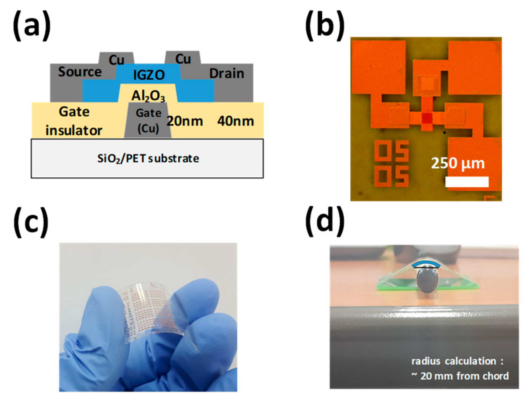
2. Experimental Procedure

Figure 1a displays the schematic cross-sectional image of the flexible IGZO TFT fabricated on the polyethylene terephthalate (PET) substrate. The substrate was attached to a silicon wafer during the whole TFT fabrication process and separated from that when the TFT fabrication was completed. First, a 50-nm-thick SiO2 buffer layer was formed on the PET by e-beam evaporation. Next, a 20-nm-thick Cu film was deposited using e-beam evaporation and patterned to form the gate electrode. Then, a gate dielectric of 40-nm-thick Al2O3 was formed, using ALD at a low temperature of 80 °C, to avoid thermal damage on the PET substrate by utilizing Al(CH3)3 (trimethylaluminum—TMA) and water as precursors. A 35-nm-thick IGZO channel layer was formed by reactive sputtering using a polycrystalline IGZO target (In2O3:Ga2O3:ZnO = 1:1:1 mol %) at room temperature (RT). A 40-nm-thick Cu film was deposited and patterned to form the source/drain electrodes. Finally, the device was thermally annealed at 150 °C for 1 hour in air. Figure 1b,c display the photographic images of the fabricated IGZO TFT on the flexible PET substrate.
The electrical parameters extracted from the representative device were as follows: A VTH of 1.8 V; a μFE of 7.3 cm2/Vs; and a subthreshold swing of 0.32 V/dec. Here, VTH was defined as the value of gate-to-source voltage (VGS) inducing the drain current (ID) of a width/length (W/L) × 10 nA at a drain-to-source voltage (VDS) of 5 V [23,24]. The mechanical stress was applied to the TFTs by using the customized bending plate with a ~20 mm bending radius (Figure 1d). The direction of bending was outward with respect to the flexible substrate (tensile stress) and parallel to the source–drain current path. The electrical properties of the devices were evaluated in the dark at RT using an Agilent 4156C precision semiconductor parameter analyzer. In addition, to remove the ambient effects on the experimental results [25,26,27], the electrical characterization was conducted in a 10 mTorr vacuum environment.

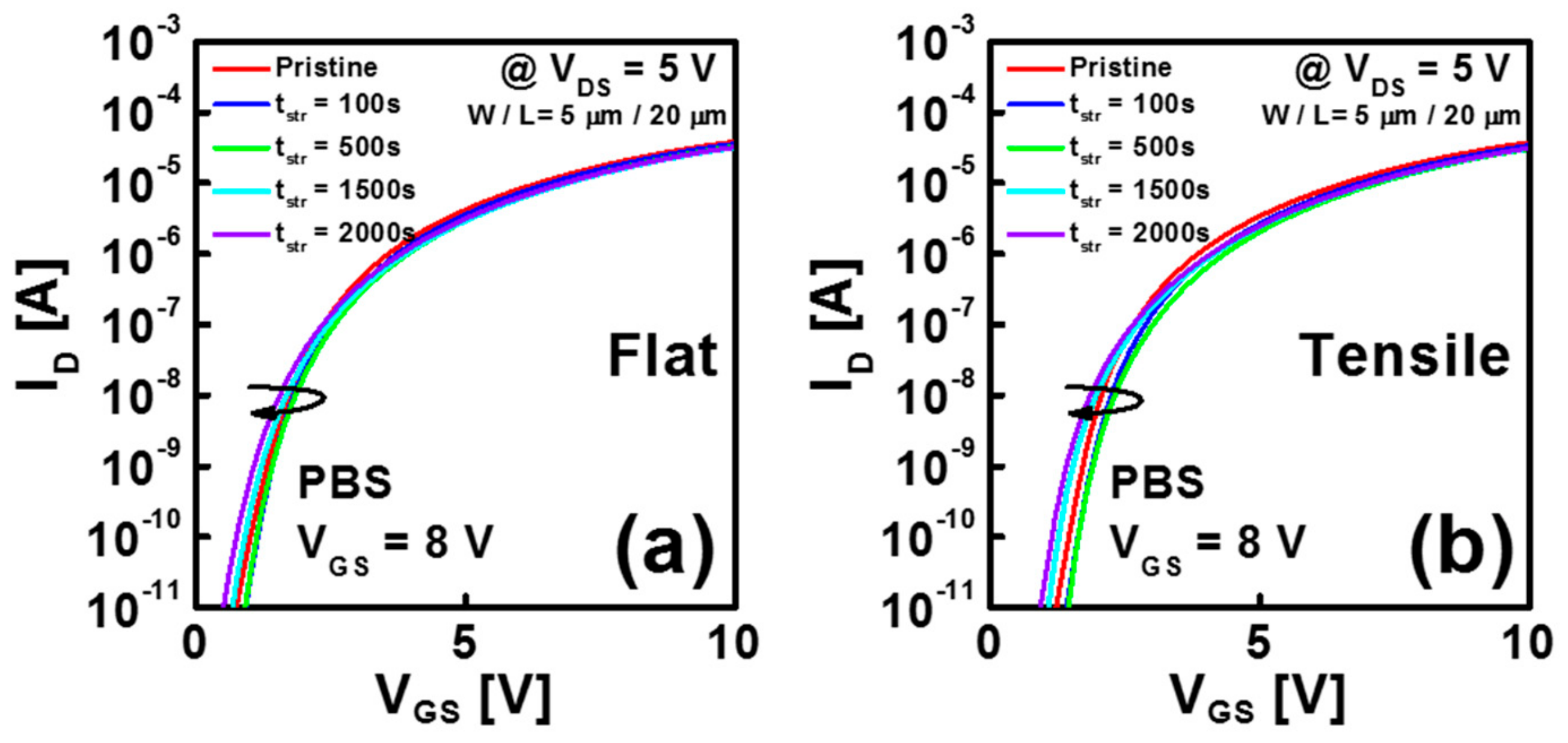
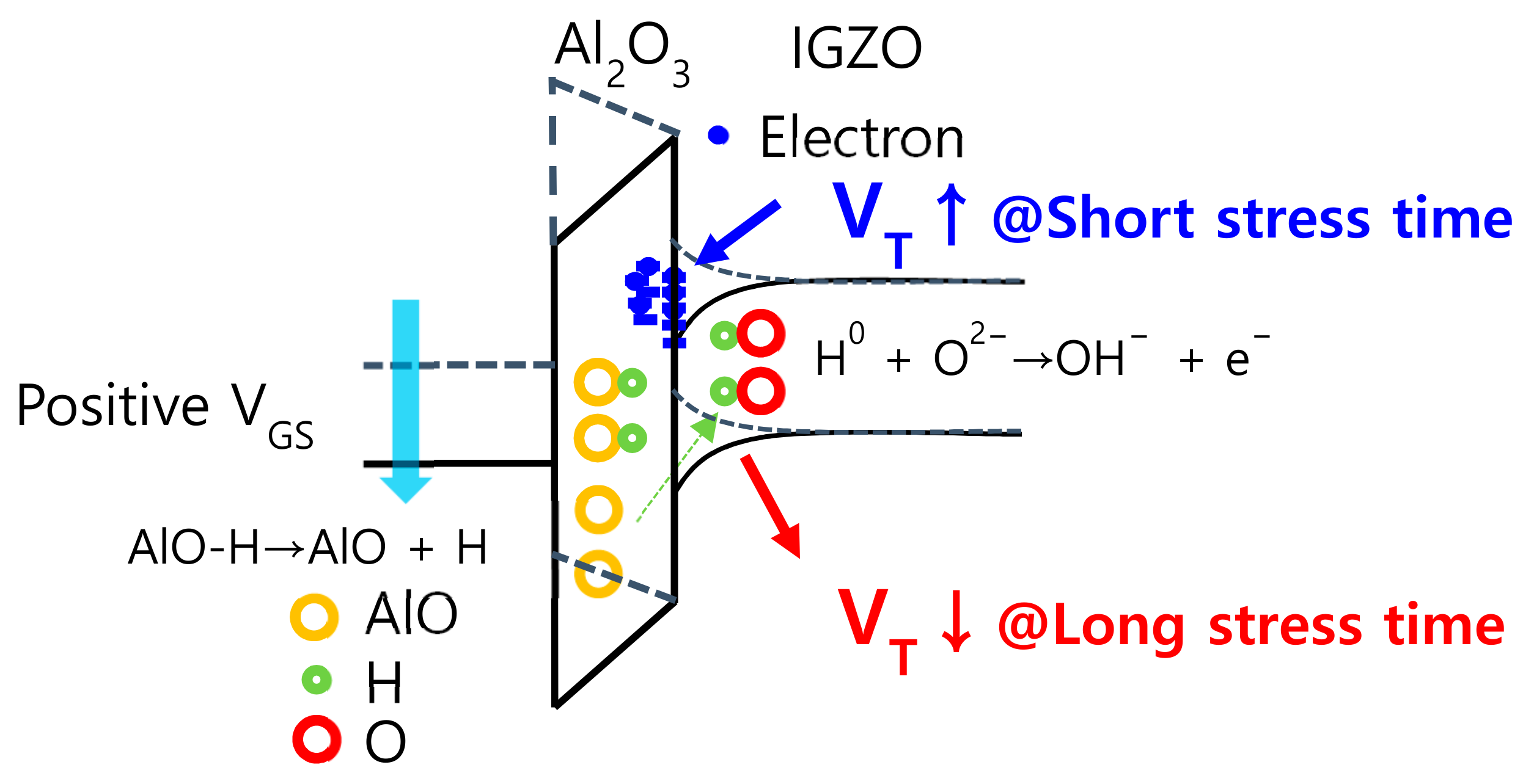
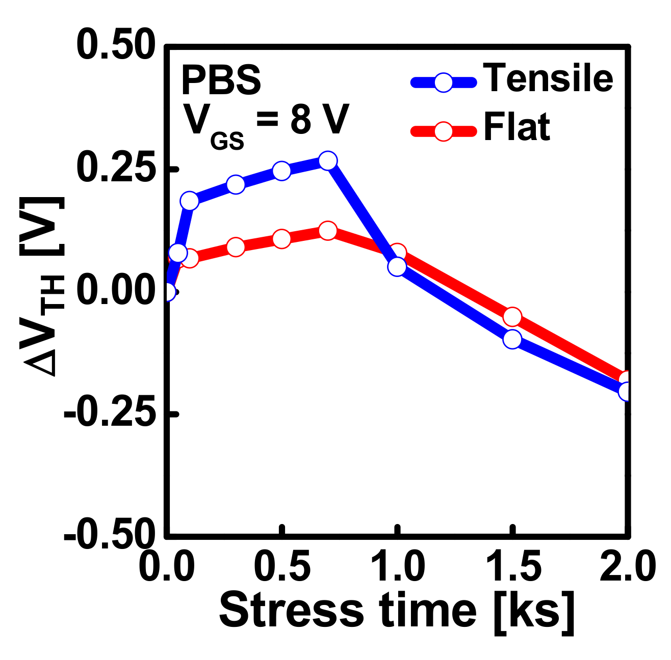
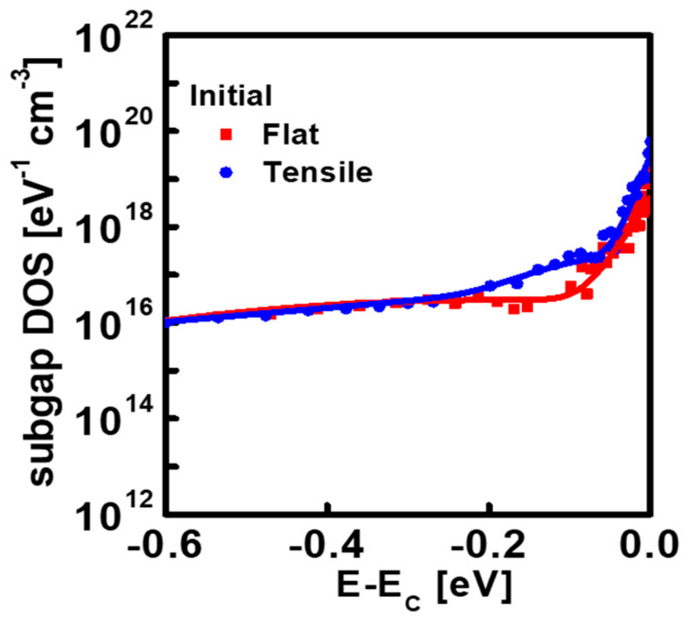
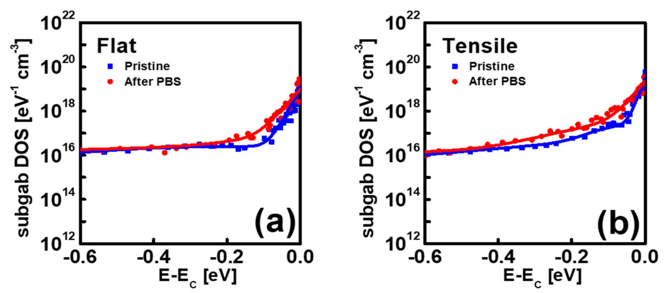
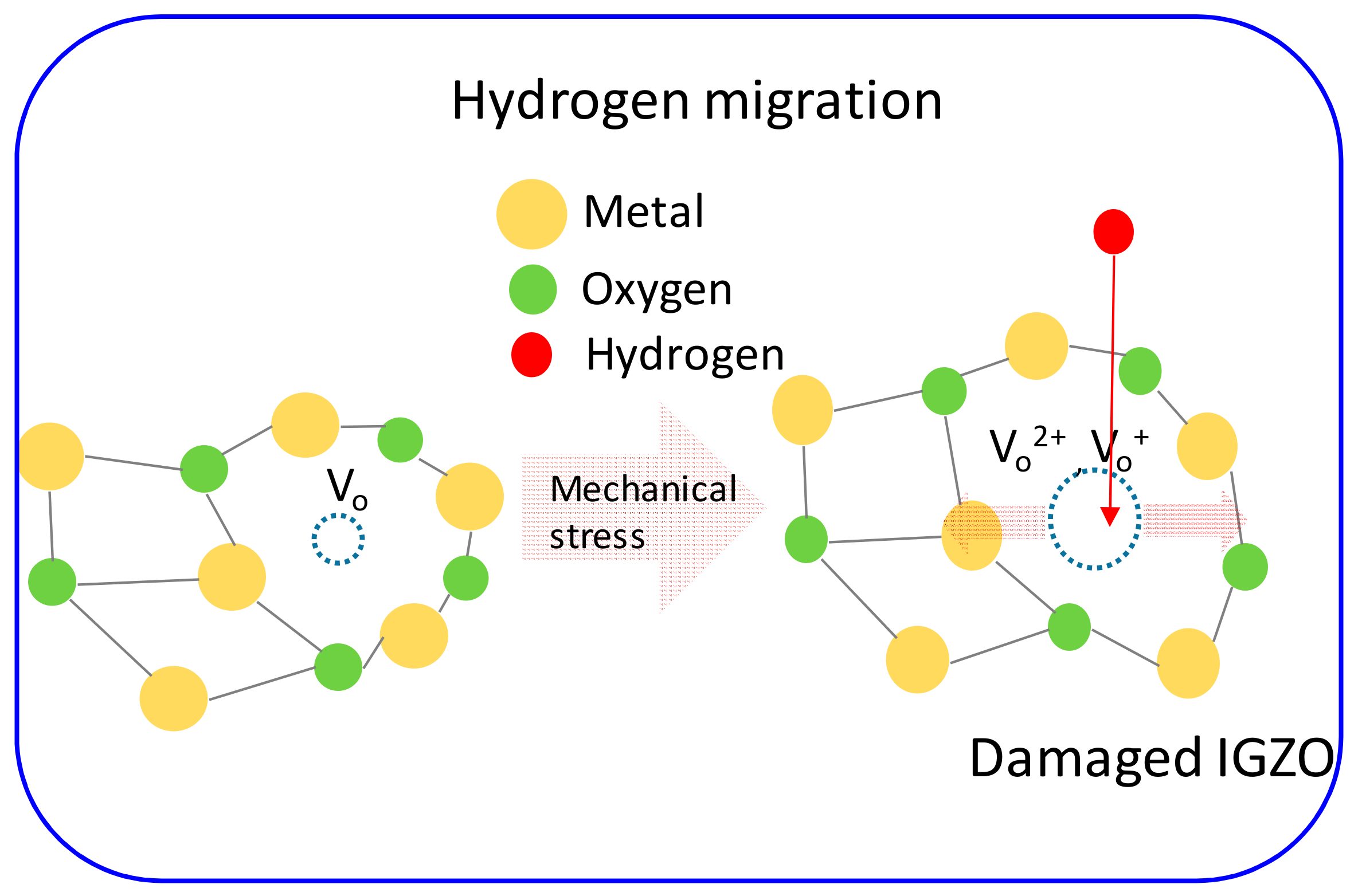
3. Results and Discussion

Figure 2a,b display the change of transfer curves as a function of the applied stress time under a positive VGS of 8 V in flexible IGZO TFTs at the flat state and under the mechanical-bending stress, respectively. Measurements were made for TFTs with a W/L of 5 μm/20 μm at a VDS of 5 V at RT. Figure 2a,b show that the IGZO TFTs exhibit VTH turnaround characteristics under both mechanical stress conditions. VTH shifts in the positive direction during the initial 500 s; but shifts in the negative direction after 500 s of stress. In previous works, the PBS-induced VTH turnaround behavior was already observed in IGZO TFTs with a low-temperature ALD Al2O3 gate dielectric and was mainly ascribed to the effect of electron trapping and hydrogen release and diffusion [28]. The positive shift of VTH at the initial stage of PBS was explained by the electron trapping in traps at the Al2O3/IGZO interface or bulk Al2O3, and the negative shift of VTH after a long stress time was mainly attributed to the hydrogen diffusion from a low-temperature ALD Al2O3 gate dielectric into an IGZO layer. The hydrogen atom was assumed to be generated from the breakage of residual AlO-H bonds in the ALD Al2O3 by the energetic electrons in the TFT channel during PBS application [28]. When Al2O3 is deposited using ALD at low temperatures, the chemical reaction between AlO-H and TMA is less complete, which causes considerable AlO-H residues in Al2O3 [29]. As hydrogen is the effective donor in IGZO through the reaction of H0 + O2−→OH + e [30], the hydrogen doping shifts the VTH. of the IGZO TFT in the negative direction.
Figure 3 displays the schematic energy band diagram which illustrates the effects of electron trapping and hydrogen release and diffusion on the VTH of IGZO TFTs. Figure 4 shows the ∆VTH versus stress time extracted from Figure 2a,b. From Figure 4, we can clearly observe that the magnitudes of ∆VTH in both the positive and negative directions exhibit larger values when a flexible IGZO TFT is subjected to the mechanical stress than when it is at the flat state. As far as we know, this is a phenomenon that has not been reported in the previous works. Considering that the IGZO TFT are subjected to the simultaneous mechanical and electrical stress when they are used for the backplane of flexible displays, it is very important to analyze the phenomenon observed in Figure 4.
To find out the physical mechanism for the observed phenomenon in Figure 4, the subgap DOS were extracted from the IGZO TFTs before and after PBS application under mechanical-bending stress and no mechanical stress, respectively, using the monochromatic photonic capacitance-voltage (C-V) technique [31]. Figure 5 displays the energy distribution of the subgap DOS obtained from the IGZO TFTs under mechanical-bending stress and no mechanical stress before PBS application, respectively. Figure 5 displays that the density of tail states near the conduction band edge (EC) extracted from the IGZO TFT under mechanical-bending stress are higher than that extracted from the TFT at the flat state, which is possibly ascribed to the larger number of structural defects at the interface in the mechanically-bended IGZO TFT due to different Young’s modulus values of Al2O3 (300 GPa) and IGZO (137 GPa) [27]. When the same strain is applied to each layer, the Al2O3 gate insulator undergoes larger stress compared to IGZO channel layer, which can generate the structural defects at the interface between Al2O3 and IGZO. As the interface trap states act as the electron trapping sites during PBS application in IGZO TFTs, it can explain the large positive shift of VTH at the initial stage of PBS in the mechanically-bended IGZO TFT in Figure 4 [32]. From Figure 5, we can also observe that not only the density of tail states but the subgap DOS at 0.1–0.3 eV below EC exhibits larger values in the mechanically-bended IGZO TFT than in the IGZO TFT at the flat state. In previous works, the mechanical strain was reported to generate the oxygen vacancies in IGZO, including ionized ones [20,21]. Considering that the increase in the donorlike states at ~EC–(0.1–0.3 eV) is most likely to result from the increase in the ionized oxygen vacancies in IGZO [33,34], an increase in the subgap DOS at 0.1–0.3 eV below EC in Figure 5 can be possibly ascribed to the increased oxygen vacancies in IGZO due to the mechanical bending stress.
Figure 6a,b compares the subgap DOS extracted from the IGZO TFTs before and after PBS application (stress time: 2000 s) at the flat state and under the mechanical-bending stress, respectively. Figure 6 shows that the subgap DOS near EC increases after PBS application under both mechanical conditions. However, it increases more pronouncely after PBS in the IGZO TFT under mechanical bending stress than that at the flat state. In previous reports, the negative shift of VTH after a long stress time was mainly attributed to the hydrogen diffusion from a low-temperature ALD Al2O3 gate dielectric into an IGZO layer [28]. As the hydrogen acts as an effective donor in IGZO, it generates the donor states near EC and shifts the VTH of the IGZO TFT in the negative direction. The PBS-induced increase of subgap DOS near EC observed in Figure 6 is possibly ascribed to the increase of the hydrogen concentration inside the IGZO after PBS application. In addition, a more pronounced increase of subgap DOS near EC in the IGZO TFT under mechanical-bending stress is considered as a result of more enhanced hydrogen diffusion from Al2O3 gate dielectric into an IGZO layer in the mechanically stressed IGZO TFT. This result is consistent with that in Figure 4, which shows a more pronounced negative shift of VTH after a long stress time in the mechanically stressed IGZO TFT. More enhanced hydrogen diffusion in the mechanically stressed IGZO TFT is believed to be caused from the increased oxygen vacancies which can act as the hydrogen hopping site in IGZO. Figure 7 displays the schematic diagram illustrating the mechanism responsible for more enhanced hydrogen diffusion form ALD Al2O3 gate dielectric into an IGZO layer in IGZO TFTs under mechanical stress.

4. Conclusions

In this research, we compared the PBS-induced instability of IGZO TFTs under the mechanical-bending stress and no mechanical stress by using the flexible IGZO TFTs fabricated with a low-temperature ALD Al2O3 gate dielectric. The IGZO TFTs exhibited a ∆VTH under an application of PBS with a turnaround behavior from the positive ∆VTH to the negative ∆VTH under both mechanical stress conditions. The magnitudes of ∆VTH in both directions exhibited higher values when a flexible IGZO TFT was mechanically bended than it was at the flat state. The observed phenomena were considered as a result of the additional interface trap generation and the enhanced hydrogen diffusion from ALD Al2O3 to IGZO by the mechanical-bending stress during an application of PBS. The subgap DOS was extracted before and after an application of PBS under both mechanical stress conditions using the monochromatic photonic C-V technique. The obtained results were correlated with a PBS-induced larger ∆VTHs in both directions under mechanical-bending stress as compared to at the flat state. To fully understand the degradation mechanism, a further study that compares the effects of simultaneous mechanical and electrical stress in flexible IGZO TFTs having Al2O3 gate dielectrics with different hydrogen contents needs to be conducted in the future.

Author Contributions

Conceptualization, Y.S., H.-I.K., and D.H.K.; experiment, Y.S., H.-S.J., H.-Y.J., S.P., J.T.J. and S.C.; data analysis, Y.S., H.-S.J., H.-Y.J., D.M.K., S.-J.C., X.J., H.-I.K., and D.H.K., writing—original draft preparation, Y.S.; supervision, H.-I.K. and D.H.K.; writing—review and editing, H.-I.K.

Funding

This work was supported by the national research foundation (NRF) of Korea funded by the Korean government under Grant 2016R1A5A1012966, 2016M3A7B4909668, 2017R1A2B4006982, 2017R1A2A2A14001213 and in part by an Electronics and Telecommunications Research Institute (ETRI) grant funded by the Korean government (18ZB1800).

Conflicts of Interest

The authors declare no conflict of interest.

References

  1. Nomura, K.; Ohta, H.; Takagi, A.; Kamiya, T.; Hirano, M.; Hosono, H. Room-temperature fabrication of transparent flexible thin-film transistors using amorphous oxide semiconductors. Nature 2004, 432, 488–492. [Google Scholar] [CrossRef] [PubMed]
  2. Geng, D.; Kang, D.H.; Jang, J. High.-performance amorphous Indium-Gallium-Zinc-Oxide thin-film transistor with a self-aligned etch stopper patterned by back-side UV exposure. IEEE Electron Device Lett. 2011, 32, 758–760. [Google Scholar] [CrossRef]
  3. Fortunato, E.; Barquinha, P.; Martins, R. Oxide semiconductor thin-film transistors: A review of recent advances. Adv. Mater. 2012, 24, 2945–2986. [Google Scholar] [CrossRef]
  4. Lee, U.G.; Mativeng, M.; Kang, D.H.; Jang, J. A Three-Mask-Processed Coplanar a-IGZO TFT with Source and Drain. Offsets. IEEE Electron Device Lett. 2012, 33, 812–814. [Google Scholar] [CrossRef]
  5. Zhang, J.; Yang, J.; Li, Y.; Wilson, J.; Ma, X.; Xin, Q.; Song, A. High performance complementary circuits based on p-SnO and n-IGZO thin-film transistors. Materials 2017, 10, 319. [Google Scholar] [CrossRef] [PubMed]
  6. Kim, K.S.; Ahn, C.H.; Kang, W.J.; Cho, S.W.; Jung, S.H.; Yoon, D.H.; Cho, H.K. An. all oxide-based imperceptible thin-film transistor with humidity sensing properties. Materials 2017, 10, 530. [Google Scholar] [CrossRef]
  7. Jeong, C.Y.; Kim, H.J.; Hong, S.Y.; Song, S.H.; Kwon, H.I. Two-stage unified stretched-exponential model for time-dependence of threshold voltage shift under positive-bias-stresses in amorphous indium–gallium–zinc oxide thin-film transistors. Jpn. J. Appl. Phys. 2017, 56, 080301. [Google Scholar] [CrossRef]
  8. Han, K.L.; Cho, H.S.; Ok, K.C.; Oh, S.; Park, J.S. Comparative Study on Hydrogen Behavior in InGaZnO Thin Film Transistors with a SiO2/SiNx/SiO2 Buffer on Polyimide and Glass Substrates. Electr. Mater. Lett. 2018, 14, 749–754. [Google Scholar] [CrossRef]
  9. Yoon, S.J.; Seong, N.J.; Choi, K.J.; Shin, W.C.; Yoon, S.M. Investigations on the bias temperature stabilities of oxide thin film transistors using In–Ga–Zn–O channels prepared by atomic layer deposition. RSC Adv. 2018, 8, 25014–25020. [Google Scholar] [CrossRef]
  10. Choi, S.B.; Kim, K.T.; Park, S.K.; Kim, Y.H. High-Mobility Inkjet-Printed Indium-Gallium-Zinc-Oxide Thin-Film Transistors Using Sr-Doped Al2O3 Gate Dielectric. Materials 2019, 12, 852. [Google Scholar] [Green Version]
  11. Hong, S.Y.; Kim, H.J.; Kim, D.H.; Jeong, H.Y.; Song, S.H.; Cho, I.T.; Noh, J.Y.; Yun, P.S.; Lee, S.W.; Park, K.S.; et al. Study on the Lateral Carrier Diffusion and Source-Drain. Series Resistance in Self-Aligned Top.-Gate Coplanar InGaZnO Thin-Film Transistors. Sci. Rep. 2019, 9, 6588. [Google Scholar] [CrossRef] [PubMed]
  12. Munzenrieder, N.; Voser, P.; Petti, L.; Zysset, C.; Buthe, L.; Vogt, C.; Salvatore, G.A.; Troster, G. Flexible Self-Aligned Double-Gate IGZO TFT. IEEE Electron Device Lett. 2014, 35, 69–71. [Google Scholar] [CrossRef]
  13. Kumaresan, Y.; Pak, Y.; Lim, N.; Kim, Y.; Park, M.J.; Yoon, S.M.; Youn, H.M.; Lee, H.; Lee, B.H.; Jung, G.Y. Highly Bendable In-Ga-ZnO Thin Film Transistors by Using a Thermally Stable Organic Dielectric Layer. Sci. Rep. 2016, 6, 37764. [Google Scholar] [CrossRef]
  14. Yao, R.; Zheng, Z.; Xiong, M.; Zhang, X.; Li, X.; Ning, H.; Fang, Z.; Xie, W.; Lu, X.; Peng, J. Low-temperature fabrication of sputtered high-k HfO2 gate dielectric for flexible a-IGZO thin film transistors. Appl. Phys. Lett. 2018, 112, 103503. [Google Scholar] [CrossRef]
  15. Jang, H.W.; Kim, H.R.; Yang, J.H.; Byun, C.W.; Kang, C.S.; Kim, S.K.; Yoon, S.M. Stability improvements of InGaZnO thin-film transistors on polyimide substrates with Al2O3 buffer layer. Jpn. J. Appl. Phys. 2018, 57, 090313. [Google Scholar] [CrossRef]
  16. Zhang, L.; Xiao, W.; Wu, W.; Liu, B. Research Progress on Flexible Oxide-Based Thin Film Transistors. App. Sci. 2019, 9, 773. [Google Scholar] [CrossRef]
  17. Fujii, M.; Uraoka, Y.; Fuyuki, T.; Jung, J.S.; Kwon, J.Y. Experimental and Theoretical Analysis of Degradation in Ga2O3–In2O3–ZnO Thin-Film Transistors. Jpn. J. Appl. Phys. 2009, 48, 04C091. [Google Scholar] [CrossRef]
  18. Lee, S.W.; Jeon, K.C.; Park, J.-H.; Kim, S.C.; Kong, D.S. Electrical stress-induced instability of amorphous indium-gallium-zinc oxide thin-film transistors under bipolar ac stress. Appl. Phys. Lett. 2009, 95, 132101. [Google Scholar] [CrossRef]
  19. Mativenga, M.; Seok, M.J.; Jang, J. Gate bias-stress induced hump-effect in transfer characteristics of amorphous-indium-galium-zinc-oxide thin-fim transistors with various channel widths. Appl. Phys. Lett. 2011, 99, 122107. [Google Scholar] [CrossRef]
  20. Liao, P.Y.; Chang, T.C.; Su, W.C.; Chen, Y.J.; Chen, B.W.; Hsieh, T.Y.; Yang, C.Y.; Huang, Y.Y.; Chang, H.M.; Chiang, S.C. Effect of mechanical-strain-induced defect generation on the performance of flexible amorphous In–Ga–Zn–O thin-film transistors. Appl. Phys. Exp. 2016, 9, 124101. [Google Scholar] [CrossRef]
  21. Billah, M.M.; Hasan, M.M.; Jang, J. Effect of Tensile and Compressive Bending Stress on Electrical Performance of Flexible a-IGZO TFTs. IEEE Electron Device Lett. 2017, 38, 890–893. [Google Scholar] [CrossRef]
  22. Jeong, H.J.; Kim, B.S.; Han, K.L.; Oh, S.; Park, J.S. Quantitative analysis of interface trap recovery caused by repetitive bending stress in flexible oxide thin-film transistors. Jpn. J. Appl. Phys. 2019, 58, 050906. [Google Scholar] [CrossRef]
  23. Lee, W.-S.; Mativenga, M.; Kang, J.-S.; Tak, N.-K.; Choi, I.-C.; Kim, J.-Y.; Han, J.-U.; Choi, J.-H.; Hwang, M.-G. Spice model for detection of dynamic threshold voltage shift during failure analysis of oxide TFT-based AMD gate drivers. J. Soc. Inf. Display 2017, 25, 663–671. [Google Scholar] [CrossRef]
  24. Kim, W.-S.; Lee, Y.-H.; Cho, Y.-J.; Kim, B.-K.; Park, K.T.; Kim, O. Effect of Wavelength and Intensity of Light on a-InGaZnO TFTs under Negative Bias Illumination Stress. ECS J. Solid State Sci. Technol. 2017, 6, Q6–Q9. [Google Scholar] [CrossRef]
  25. Jeong, J.K.; Yang, H.W.; Jeong, J.H.; Mo, Y.-G.; Kim, H.D. Origin of threshold voltage instability in indium-gallium-zinc oxide thin film transistors. Appl. Phys. Lett. 2008, 93, 123508. [Google Scholar] [CrossRef]
  26. Jeong, H.-S.; Park, M.-J.; Kwon, S.-H.; Joo, H.-J.; Kwon, H.-I. Highly sensitive and selective room-temperature NO2 gas-sensing characteristics of SnOX-based p-type thin-film transistor. Sens. Actuators B Chem. 2019, 288, 625–633. [Google Scholar] [CrossRef]
  27. Jeong, H.J.; Han, K.L.; Ok, K.C.; Lee, H.M.; Oh, S.; Park, J.S. Effect of mechanical stress on the stability of flexible InGaZnO thin-film transistors. J. Inf. Disp. 2017, 18, 87–91. [Google Scholar] [CrossRef] [Green Version]
  28. Chang, Y.H.; Yu, M.J.; Lin, R.P.; Hsu, C.P.; Hou, T.H. Abnormal positive bias stress instability of In–Ga–Zn–O thin-film transistors with low-temperature Al2O3 gate dielectric. Appl. Phys. Lett. 2016, 108, 033502. [Google Scholar] [CrossRef]
  29. Dillon, A.C.; Ott, A.W.; Way, J.D.; George, S.M. Surface chemistry of Al2O3 deposition using Al(CH3)3 and H2O in a binary reaction sequence. Surf. Sci. 1995, 322, 230–242. [Google Scholar] [CrossRef]
  30. Kamiya, T.; Nomura, K.; Hosono, H. Origins of High. Mobility and Low Operation Voltage of Amorphous Oxide TFTs: Electronic Structure, Electron. Transport Defects and Doping. J. Disp. Tech. J. Disp. Technol. 2009, 5, 468–483. [Google Scholar] [CrossRef]
  31. Bae, H.; Choi, H.; Jun, S.; Jo, C.; Kim, Y.H.; Hwang, J.S.; Ahn, J.; Oh, S.; Bae, J.-U.; Choi, S.-J.; et al. Single-scan monochromatic photonic capacitance-voltage technique for extraction of subgap DOS over the bandgap in amorphous semiconductor TFTs. IEEE Electron Dev. Lett. 2013, 34, 1524–1526. [Google Scholar] [CrossRef]
  32. Lee, J.M.; Cho, I.T.; Lee, J.H.; Kwon, H.I. Bias-stress-induced stretched-exponential time dependence of threshold voltage shift in InGaZnO thin film transistors. Appl. Phys. Lett. 2008, 93, 093504. [Google Scholar] [CrossRef]
  33. Migliorato, P.; Chowdhury, M.D.H.; Um, J.G.; Seok, M.J.; Jang, J. Light/negative bias stress instabilities in indium gallium zinc oxide thin film transistors explained by creation of a double donor. Appl. Phys. Lett. 2012, 101, 123502. [Google Scholar] [CrossRef]
  34. Revenant, C.; Benwadih, M.; Proux, O. Local structure around Zn and Ga in solution-processed In-Ga-Zn-O and implications for electronic properties. Phys. Status Solidi RRL 2015, 9, 652–655. [Google Scholar] [CrossRef]
Figure 1. (a) Schematic cross-sectional image of the flexible indium-gallium-zinc oxide (IGZO) thin-film transistor (TFT) fabricated on the polyethylene terephthalate (PET) substrate. (b), (c) Photographic images of the fabricated flexible IGZO TFT. (d) Photographic image of the customized bending plate with a ~20 mm bending radius.
Materials 12 03248 g001
Figure 2. Change of transfer curves as a function of the applied stress time under a VGS stress of 8 V in flexible IGZO TFTs (a) at the flat state and (b) under the mechanical-bending stress.
Materials 12 03248 g002
Figure 3. Schematic energy band diagram which illustrates the effects of electron trapping and hydrogen release and diffusion on the VTH of IGZO TFTs.
Materials 12 03248 g003
Figure 4. ∆VTH versus stress time under a VGS stress of 8 V in flexible IGZO TFTs at the flat state and under tensile bending stress.
Materials 12 03248 g004
Figure 5. Energy distribution of the subgap density of states (DOS) obtained from the IGZO TFTs before positive-bias-stress (PBS) application under the tensile bending stress and no mechanical stress.
Materials 12 03248 g005
Figure 6. Energy distribution of the subgap DOS obtained from the IGZO TFTs before and after PBS application (stress time: 2000 s) (a) at the flat state and (b) under tensile bending stress.
Materials 12 03248 g006
Figure 7. Schematic diagram illustrating the physical mechanism responsible for more enhanced hydrogen diffusion form atomic layer deposition (ALD) Al2O3 gate dielectric into an IGZO layer in IGZO TFTs under mechanical bending stress.
Materials 12 03248 g007

