Ferroelectromagnetic Properties of PbFe1/2Nb1/2O3 (PFN) Material Synthesized by Chemical-Wet Technology


Institute of Technology and Mechatronics, Faculty of Computer Science and Material Science, University of Silesia in Katowice, 12 Zytnia St., 41–200 Sosnowiec, Poland
*
Author to whom correspondence should be addressed.
Materials 2018, 11(12), 2504; https://doi.org/10.3390/ma11122504
Submission received: 2 November 2018
/
Revised: 26 November 2018
/
Accepted: 4 December 2018
/
Published: 9 December 2018
Abstract
:In this work, PbFe1/2Nb1/2O3 (PFN) ceramic samples synthesized by chemically wet method (precipitation from the solution) were obtained. Due to the tendency to form powder agglomerates, the synthesized powder was subjected to ultrasound. The sintering was carried out under various technological conditions, mainly through controlling the sintering temperature. -X-ray powder-diffraction (XRD), scanning electron microscope (SEM) microstructure analysis, as well as the examinations of dielectric, ferroelectric, and magnetic properties of the PFN ceramics were carried out. Studies have shown that hard ceramic agglomerates can be partially minimized by ultrasound. Due to this treatment, closed porosity decreases, and the ceramic samples have a higher density. Optimization and improvement of the technological process of the PFN material extends the possibility of its use for the preparation of multiferroic composites or multicomponent solid solutions based on PFN. Such materials with functional properties find applications in microelectronic applications, e.g., in systems integrating ferroelectric and magnetic properties in one device. The optimal synthesis conditions of PFN ceramics were determined to be 1050 °C/2 h.
1. Introduction
Ferroelectromagnetic PbFe1−xNbxO3 (PFN) material is a member of the perovskite-like family of the general formula A(B′B″)O3, exhibiting multiferroic properties. Ions of lead locate to A position, while ions of niobium and iron are substituted randomly to octahedral positions B′ and B″ [1,2]. Multiferroics are materials which show simultaneously at least two types of physical (ferroic) states e.g., a ferromagnetic state (antiferromagnetic, ferrimagnetic) [3], a ferroelectric state (antiferroelectric, ferrielectric), a ferroelastic state (ferromagneticelastic, ferroelastoelectric), and a ferrotoroid state [4,5,6,7,8,9]. In the PFN materials, iron has a natural magnetic moment (connecting Fe-O-Fe in the angle of 180° ensures an optimum state of magnetic order occurrence [10]). Smart materials are used extensively in automation, control processes, robotics, micromechatronic applications, material processing, aerospace engineering, the automotive and electronic industries, defence technology, medical technology and biotechnology [11,12,13,14,15]. On the other hand, the piezoelectric transduction mechanism is also an efficient mechanism for nanoelectronics and microelectronics [16,17].
During the technological process of the PFN ceramic material, many methods and techniques are used, e.g., a sol-gel synthesis, molten salt synthesis, precipitation from the solution, reaction in solid state, two-stage columbite method, and mechanical activation (high-energy milling) [18,19,20,21,22,23,24,25,26]. Each of the above-mentioned methods and techniques require the use of specific technological conditions and diligence in laboratory process in order to obtain materials with good properties. Precipitating nanoparticles from the solution of chemical compounds can be classified into five categories: colloidal methods (precipitation processes), sol–gel processing, water–oil micro-emulsions method, hydrothermal synthesis, and polyol method. The main benefits of liquid phase synthesis are a high purity and uniform nanostructure achievable at low temperatures. Generally, the sol-gel process consists in the chemical transformation of a liquid (sol) into a gel state (in various forms), and subsequently, a transition into solid powders (during further processing). The sol-gel method, and the numerous varieties thereof, allowing one to obtain a ceramic powder with optimal parameters at low synthesis temperatures, which provides preservation of the stoichiometric composition. The sol-gel synthesis may be used to prepare materials with different shapes, i.e., dense or porous structures, thin fibres, thin films etc. [27,28,29,30,31]. The advantages of the solution–precipitation method in the technological process of the synthesis of ceramic materials are a high purity and a uniform nanostructure achievable at low temperatures. PFN ceramics can be used in modern microelectric and micromechatronic applications, such as piezoelectric transducers, sensors, generators, servomotors, actuators, phase modulators, frequency multipliers, multilayer ceramic capacitors (MLCC), and memory elements [2,32].
It has already been shown that single-phase PFN materials reveal weak magnetoelectric coupling [33,34]. The improvement of the known technological methods and the optimization of the technological process allows one to obtain a PFN material with repetitive properties and optimal operational parameters. In order to further improve the electrophysical properties and increase the application functionality, the PbFe1/2Nb1/2O3 material can be used, for instance, to obtain multicomponent solid solutions [34,35,36,37,38], to further modify the basic composition with appropriate admixtures [39,40,41], or as an element of ceramic composite ferroelectromagnetics [42] in micromechatronic applications, integrating various properties in one system.
The aim of the work is to obtain and study the ferroelectromagnetic PFN ceramics synthesized by a chemical-wet technology (solution precipitation method) and sintered by conventional pressureless methods. As a result of the technological process used, the PFN ceramic powder tended to combine into large, hard agglomerates. In order to minimize this adverse phenomenon, at the initial stage of the process, the powder agglomerates were subjected to ultrasound disruption.
The crystal structure, microstructure, DC electric conductivity, magnetic, dielectric, and ferroelectric properties of the PFN samples were investigated.
2. Experiment
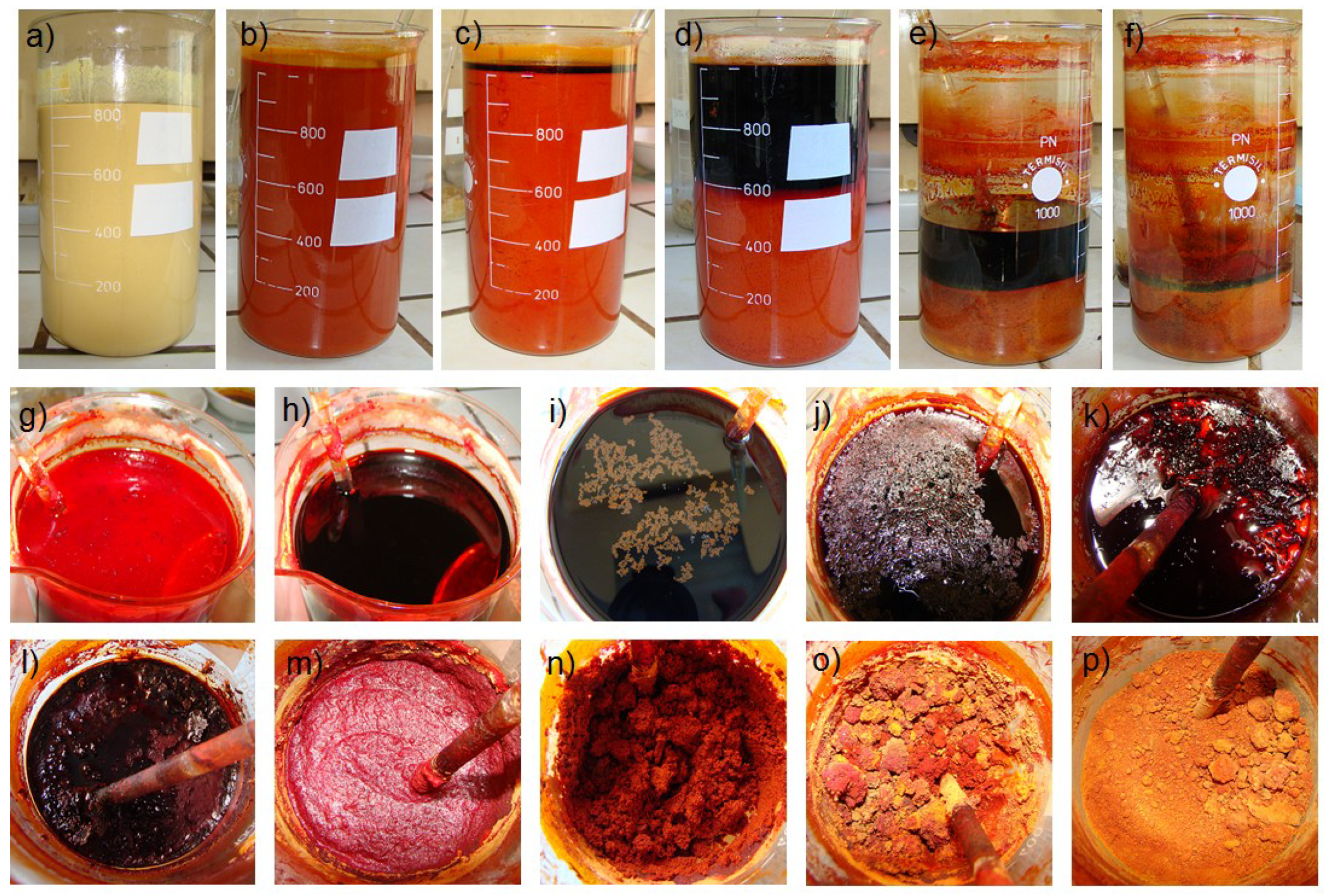
The synthesized ceramic PbFe1−xNbxO3 (PFN) powder was obtained by a chemical-wet technology—the solution precipitation method [24] (a variation of the sol-gel method). In the technological process (Figure 1), there were the following precursors: ferric citrate monohydrate C6H5FeO7⋅H2O (pure p.a., Fluka, Neu-Ulm, Germany), lead (II) acetate trihydrate Pb(CH3COO)2⋅3H2O (pure p.a., POCH), and niobium (V) ethoxide Nb(OC2H5)5 (99.95%, Aldrich, Saint Louis, MO, USA). Lead acetate trihydrate was dissolved in the CH3COOH acetic acid, and simultaneously Nb(OC2H5)5 ethylene glycol (POCH) with 2-methoxyethanol (Fluka) was added. Subsequently, distilled water was added to ferric citrate monohydrate (the solution was heated). Next, acetic acid was added to increase the effectiveness of dissolving and it was brought to boiling (with vigorous stirring). Consecutively, all of the ingredients were mixed together and acetylacetone was added, with the entire mixture being heated simultaneously. In the next stage, distilled water was added for the hydrolysis process and the precipitation process started. The obtained liquid solution was dried under an IR lamp (allowing evaporation of the solvent to occur faster, producing a ceramic powder in the final stage). After completion of drying the powder was mixed, after which the removal of organic parts was done by calcination route at 600 °C/3 h. As a result of the technological process, fine-grained a ceramic powder was obtained.
The obtained fine-grained ceramic powder of PFN, during the technological process, tended to form numerous agglomerates, which promoted the formation of a significant closed porosity in the volume of ceramic samples [24]. Since the optimization of powder mixing parameters used during the experiment as well as the extension of the mixing time did not eliminate the tendency to form hard, strongly compact powder agglomerates, an additional step in powder technology was applied. In order to minimize this unfavorable phenomenon, the process of breaking up agglomerates with ultrasound was carried out in an ultrasonic cleaner.
In the subsequent stage, the PFN powder was mixed and then pressed into pellets. Densification was made by the free sintering method (obtaining three ceramic samples) at the following conditions (Ts/ts): (i) 1025 °C/2 h (P-1u), (ii) 1050 °C/2 h (P-2u), (iii) 1075 °C/2 h (P-3u). As the obtained PFN ceramic samples have closed porosity, the ceramic powder was again mixed in a ball mill for 24 h, and then the powder was twice calcined at 600 °C/2 h. After these treatments, the ceramic powder was pressed into pellets and densification was conducted by the free sintered method, at the following conditions: (iv) 1050 °C/2 h (P-4u).
For the electrical measurements, sintered pellets with a thickness of 1.0 mm were prepared. The mechanical stress was removed by the annealing process (750 °C/0.25 h), and surfaces of the samples were covered with a silver electrode at 850 °C/0.25 h (method of firing a silver paste).
X-ray powder-diffraction data (XRD) of the PFN material were performed on a Phillips X’Pert APD diffractometer (PANalytical, Eindhoven, The Netherlands) at room temperature (Cu-Kα radiation, in the 2θ range from 10° to 65°, in steps of 0.02°, with an integration time of 4 s/step). The surface morphology and stoichiometry of the PFN ceramics were tested on a JSM-7100F TTL LV (Jeol Lid., Tokyo, Japan) scanning electron microscope (the samples were coated with gold to provide electrical conductivity in order to obtain charging effects). Temperature dielectric measurements were performed on a LCR meter (QuadTech 1920 Precision LCR Meter, QuadTech, Inc., Maynard, MA, USA) and DC electrical conductivity was carried out using a Keithley 6517B electrometer (Keithley Instruments, Cleveland, OH, USA), in a temperature range from 20 °C to 420 °C (a heating cycle).
Ferroelectric properties were carried out using a Sawyer-Tower circuit and a high voltage amplifier (Matsusada Inc. HEOPS-5B6 precision, Matsusada Precision Inc., Kusatsu, Japan). The experimental data were stored on a computer disc using an A/D, D/A transducer card (National Instruments Corporation, Austin, TX, USA). The DC magnetic susceptibility measurements were carried out by the Cahn magnetic balance (H0 = 800 Oe).
3. Results and Discussion
3.1. X-Ray Diffraction Analysis
At room temperature, the PFN ceramic material obtained by the solution precipitation method has shown a perovskite structure with a small amount of the pyrochlore phase (Pb2Nb2O7). The best match results (Figure 2) were obtained for the pattern (JCPDS card No. 04-009-5124), with tetragonal symmetry and P4mm space groups (the unit cell parameters: a0 = 4.0070 Å, b0 = 4.0070 Å, c0 = 4.0130 Å, and α = 90°). From the integrated intensities of the fitted peaks, the perovskite phase in the ceramic PFN powder was estimated using the Equation (1)
where I110 and I222 are integrated intensities of the most intense (110) perovskite and (222) pyrochlore diffraction lines. The percentage content of the perovskite phase in the PFN ceramic material is 94.64.
3.2. Microstructural Properties
The surface morphology of the fracture PFN samples with different technologies is shown in Figure 3. The microstructure of the P-1u sample shows grain size heterogeneity with clearly visible grain boundaries. In the microstructure, there are both small and large grains with incomplete crystallization. In the case of the P-2u and P-4u samples, the microstructure is characterized by properly crystallized grains, but with visible porosity. The sample breakthrough occurs mainly through grain boundaries, which is confirmed by the properly selected technological sintering conditions of the ceramic, ensuring high mechanical strength of the grain interior. In the case of the P-3u sample, additional stages of the technological process have caused higher grains in the microstructure. The breakthrough of the sample takes place predominantly through the grain, however breaks occurs in a compact solid manner. This behavior indicates high mechanical strength in the grain boundaries, at the expense of the interior of the grains. Activation of ultrasound on the ceramic powder of PFN, after the synthesis process, partially breaks hard powder agglomerates. As a result, the PFN ceramics have a higher density, with a smaller amount of closed porosity.
The energy dispersive spectrometry (EDS) analysis (average of ten randomly chosen areas from the specimen surface) of the PFN ceramic samples confirmed the presence of constituent elements in the obtained materials. In Figure 4, all analyzed PFN samples have characteristic peaks, derived from constituent elements, differing slightly in the intensity of reflections (without the presence of peaks coming from other elements). The calculated percentage of the individual components of the PFN ceramics was summarized in Table 1. The EDS analysis of the element distribution revealed some differences in the chemical composition. All deviations between the theoretical content of chemical elements and their real content are within an acceptable range. In the case of the P-1u and P-2u samples, iron and lead deficiency and a small excess of niobium are observed, while in the case of the P-3u and P-4u samples there is a small excess of iron. The highest percentage deviation from the theoretical composition is for the P-1u samples sintered at the lowest temperature. The EDS research confirmed that the technological process of the PFN ceramics was performed correctly (no significant deviations from the assumed composition).
3.3. DC Electrical Conductivity Measurements
The ρDC resistivity at room temperature of the PFN samples is typical for semiconductors and is summarized in Table 1. The highest resistivity is revealed by the P-2u sample (1.4 × 10⁷ Ω m), while smaller is for the P-4u one (6.1 × 10⁵ Ω m). In the case of the P-4u ceramic samples, additional stages of the technological process led to increased electric conductivity (Figure 5). It is may be connected both with lower resistance of the ceramic grains, as well as grain boundaries (i.e., a temperature effect of synthesis associated with irreversible chemical changes on the grain boundaries [43]). The PFN ceramic materials exhibit n-type conductivity, which may be determined by the oxygen deficiency [44]. The oxygen deficiency results in the formation of oxygen vacancies in the crystal lattice (donor centres because of ionisation processes). The reduction processes may lead to the creation of oxygen vacancies or valency change in Nb5+ and Fe3+ ions and the formation of lattice defects (i.e., VO, , , ) and complexes and , which can be donor centers. Nonstoichiometry in the oxygen sublattice can be a result of reduction processes proceeding at high temperature, during technological process of the perovskite-type materials [44].
Activation energy for PFN ceramic samples was calculated according to Arrhenius’ law (Equation (2)) [45]:
where σ0 is pre-exponential factor, kB is Boltzmann’s constant, T is absolute temperature, and EAct is the activation energy appointed from the slope of lnσDC vs. 1/T plot. The values of the activation energy EAct at three specific regions (selected in Figure 5) are summarized in Table 2. Activation energy of the conductivity in the first region is rather small (from 0.146 eV for P-2u sample to 3.02 eV for P-3u sample). In this region, the activation energy is mostly connected with charge carrier mobility. It is shown on a hopping mechanism of the conductivity associated with the occurence of oxygen vacancies and valency change of transition elements Fe and Nb [46].
3.4. Dielectric Properties
The temperature dependences of dielectric permittivity (ε) for the PFN ceramic samples are presented in Figure 6. For the P-1u samples, both at room temperature and at the temperature of the phase transition with increasing sintering temperature, the values of dielectric permittivity increase. For 1 kHz and RT value the dielectric permittivity is 4207, 4210, and 5650, for the P-1u, P-2u, and P-3u samples, respectively. In the case of the P-4u sample, additional stages in the technological process caused an additional increase in the value of dielectric permittivity maximum (Figure 6d, Table 2). Differences in the value of the dielectric permittivity maximum of the PFN material (Table 2) resulted from different sizes and shapes of the ceramic grains of the samples. In the case of the materials with a perovskite structure, lower density and microstructure samples with poorer grain show a stronger phase transition blur.
The PFN ceramics obtained by the precipitation method (and subjected to ultrasounds) revealed a diffuse phase transition. Broadening of the phase transition is manifested by the “flattening” of the temperature dependence ε(T), i.e., the reduction in the height of the εmax (in this case the temperature corresponding to the εmax is determined by Tm). Broadening of the phase transition in materials with a perovskite structure may be associated with the occurrence of local deviations from the chemical composition in the micro-areas of ceramics (in the case of the PFN ceramics, its related to disorder in the distribution of B-side ions in the perovskite unit cell), as well as a result of the heterogeneity of the distribution of defects and mechanical stresses in grains. These factors can be the corners of the formation of a new phase at temperatures quite distant from the Curie temperature (TC) of the material. The broad phase transition in the PFN ceramics is also affected by the degree of powder compaction during the technological process, as well as the thickness of ceramic samples prepared for electrical tests. Differences in the value of the dielectric permittivity maximum of the obtained PFN samples also resulted from different sizes and shapes of the ceramic grains of the samples. In the case of the ceramic materials (with a perovskite structure), samples with lower density and microstructures with poor angularity of grains show increased broadening of the phase transition.
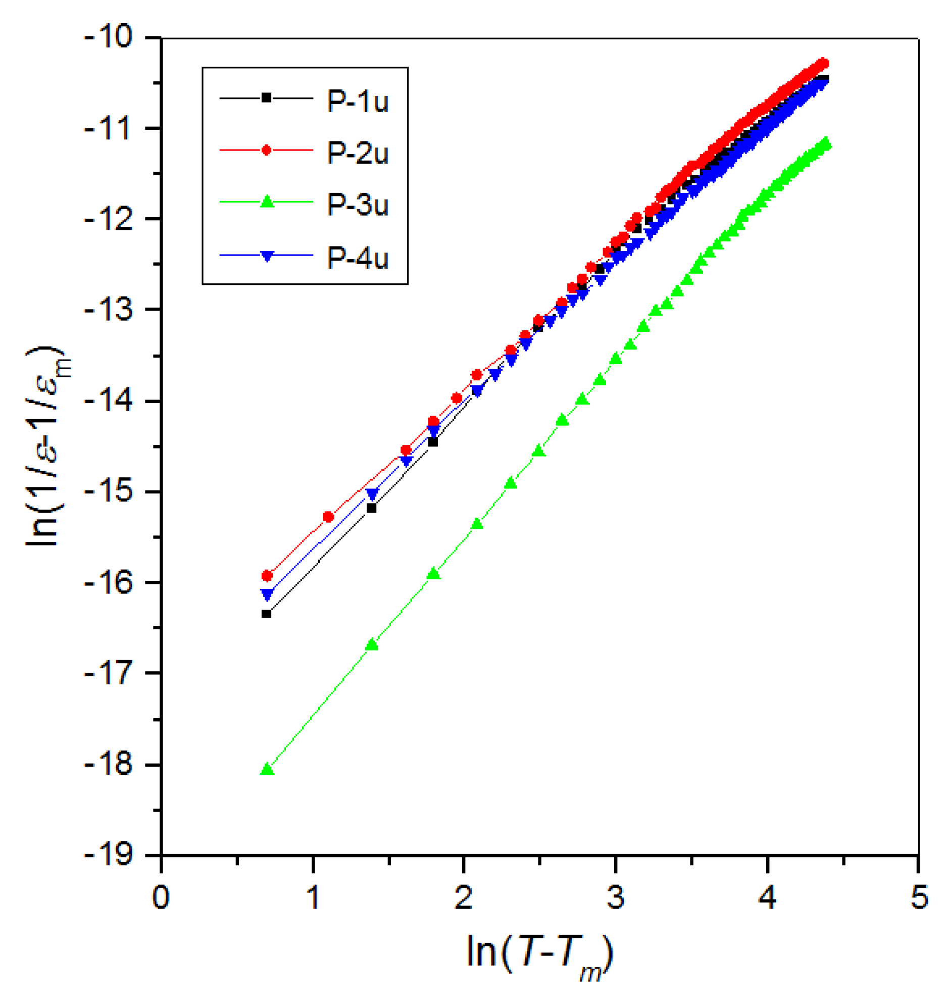
In order to evaluate the phase transition, we used the modified Curie–Weiss law (Equation (3)) [2]
where εm is the maximum value of dielectric constant, Tm is temperature of the value dielectric permittivity maximum, C represents Curie–Weiss parameter, and α is the parameters indicating the degree of blur of the phase transition and indicated ferroelectric relaxation behavior. In this case, α = 1 indicates normal Curie-Weiss behavior, while α = 2 represents a relaxor phase transition. The α parameter can be calculated by the slope of the graph plotted between ln(1/ε − 1/εm) and ln(T − Tm) under 100 Hz (Figure 7) [48]. The α parameter calculated for the P-1u sample is 1.73, for the P-2u sample is 1.61, for the P-3u sample is 1.95, and for the P-4u sample is 1.58.
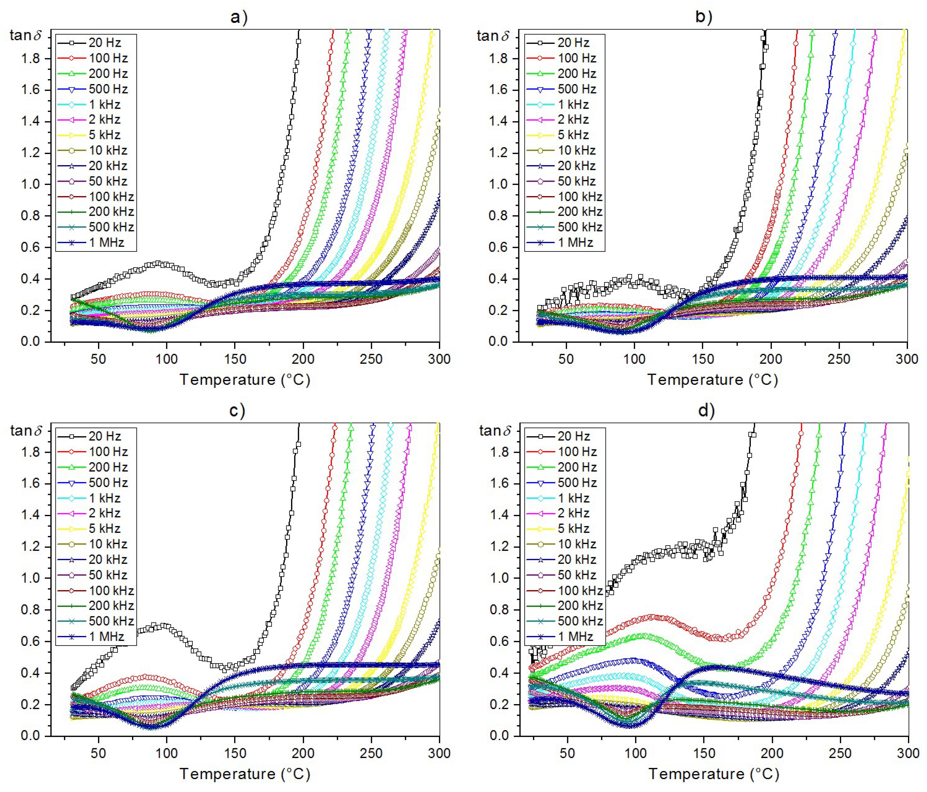
The temperature dependences of dielectric loss tangent (tanδ) for the ceramic PFN samples are presented in Figure 8. At room temperature RT and for 1 kHz, the value of tanδ is 0.148, 0.123, 0.136, 0.265, for the P-1u, P-2u, P-3u, and P-4u, respectively. From RT until about 150 °C, the dielectric loss for the PFN samples is low. Above this temperature (150 °C), a rapid growth of the dielectric loss is visible. The lowest dielectrc loss is shown in the PFN sample. The use of additional treatments in the technological process increases dielectric loss throughout the entire measurement area.
The conducted temperature tests of the dielectric properties of the ceramic PFN samples showed both high values of dielectric permittivity and low dielectric loss. This is extremely important from the point of view of designing ceramic composites with ferroic properties. Typically, in this type of ferroelectromagnetic ceramic composite, a magnetic component (for example a ferrite exhibiting much lower resistivity) will degrade the dielectric properties of the entire composite.
3.5. Ferroelectric Properties
The P-E hysteresis loops (examined at room temperature, at a frequency from 100 MHz to 20 Hz) of the PFN samples are presented in Figure 9. For all PFN samples (except for P-4u), P-E tests at room temperature showed that with increasing frequency, the saturation of hysteresis loops increases. In the case of P-1u and P-3u samples, at low frequencies, the loops have a characteristic shape for ceramic materials with losses. For 10 Hz, the value of remnant polarization PR is 6.76 µC/cm2, 5.63 µC/cm2 and 8.24 µC/cm2, and the coercive field EC is 0.785 kV/mm, 0.536 kV/mm and 0.824 kV/mm for P-1u, P-2u, and P-3u, respectively.
Despite having the lowest values for the remnant polarization and the coercive field, the hysteresis loop of the P-2u sample is narrow and shows the highest saturation for all frequencies of the measurement field. This confirms that for PFN ceramics sintering at 1050 °C is the most advantageous.
3.6. Magnetic Properties
Temperature measurements of magnetic susceptibility χσ for the PFN ceramics are presented in Figure 10. Two peaks can be observed on the temperature plots. A small peak (TN1) appears near the temperature of −112 °C, and a second one (TN2) at a temperature of about −262 °C is more visible. The anomalies appearing on the plots are connected with the occurrence of phase transitions in the magnetic material [49]. At TN1 (~−112 °C), the peak determines the magnetic transition (paramagnetic/antiferromagnetic), while the peak at TN2 (~−262 °C) is probably related to AFM-to-AFM transition [22]. The values of magnetic susceptibility decrease with an increase in the PFN ceramics’ sintering temperature, but the trend of all curves is similar. In the case of the P-4u sample, the curves are not significantly different from the P-2u sample.
4. Conclusions
The paper presents the chemical-wet technological process (precipitation from the solution) of ferroelectromagnetic PbFe1/2Nb1/2O3 ceramic powders subjected to ultrasound. The PFN material was obtained in various technological conditions and XRD, SEM, ferroelectric, dielectric, and magnetic tests were carried out. Chemically-wet methods of obtaining PFN ceramic powder have many advantages, but they also have some drawbacks. One of the disadvantages for the precipitation from the solution method is a strong tendency for the powder to combine into the form of hard agglomerates, which promotes the formation of porosity in the closed ceramic sample. Optimization of powder mixing parameters and prolonged mixing time of powders do not result in eliminating this unfavorable phenomenon. Ultrasound treatment of the PFN ceramic powder enables the partial reduction of the hard powdery agglomerates, from which the material exhibits a smaller amount of closed porosity.
At RT, the PFN material has shown a perovskite structure with small amount of the pyrochlore phase. The SEM microstructure analysis of the ceramic samples showed that the most correctly crystallizing grain has a sample obtained under the conditions of 1050 °C/2 h. Increasing the sintering temperature causes an increase in the average grains. At room temperature, the PFN ceramic samples show both ferroelectric and magnetic properties. Sintering temperatures that are either too low or too high deteriorate the dielectric properties of the PFN ceramic samples. The high sintering temperature (1300 °C) also contributes to excessive grain growth, as well as increasing the heterogeneity of the microstructural ceramic sample. Deprivation of homogeneity of the microstructure deteriorates the set of final electrophysical parameters of the PFN ceramic samples. Optimization of PFN technology extends the possibility of using this material to obtain multiferroic composites or multicomponent solid solutions based on PFN, for use in targeted applications in systems integrating ferroelectromagnetic properties in one device e.g., in microelectronic applications. The optimal sintering temperature for the PFN ceramic material obtained by chemical-wet technology under the previously listed conditions is 1050 °C/2 h.
Author Contributions
D.B.—the main author and originator of the work, he carried out research on X-ray, SEM and dielectric properties of the ceramic samples. He performed the interpretation of these results and developed the interpretation of the most measurements at the work. P.N. participated in the technology of obtaining ceramic samples, performed P-E tests and measurements of electrical conductivity of ceramic samples and developed the interpretation of results.
Funding
This research received no external funding.
Conflicts of Interest
The authors declare no conflicts of interest.
References
- Das, R.N.; Pramanik, P. Single step chemical synthesis of lead based relaxor ferroelectric niobate fine powders. Nanostruct. Mater. 1999, 11, 323–330. [Google Scholar] [CrossRef]
- Raymond, O.; Font, R.; Suarez, N.; Portalles, J.; Siqueiros, J.M. Effects of two kinds of FeNbO4 precursors in the obtainment and dielectric properties of PFN ceramics. Ferroelectrics 2003, 294, 141–154. [Google Scholar] [CrossRef]
- Kozii, V.; Ruhman, J.; Fu, L.; Radzihovsky, L. Ferromagnetic transition in a one-dimensional spin-orbit-coupled metal and its mapping to a critical point in smectic liquid crystals. Phys. Rev. B 2017, 96, 094419. [Google Scholar] [CrossRef]
- Lente, M.H.; Guerra, J.D.S.; de Souza, G.K.S.; Fraygola, B.M.; Raigoza, C.F.V.; Garcia, D.; Eiras, J.A. Nature of the magnetoelectric coupling in multiferroic Pb(Fe1/2Nb1/2)O3 ceramics. Phys. Rev. B 2008, 78, 054109. [Google Scholar] [CrossRef]
- Khomskii, D. Classifying multiferroics: Mechanisms and effects. Physics 2009, 2, 20. [Google Scholar] [CrossRef]
- Wang, K.F.; Liu, J.-M.; Ren, Z.F. Multiferroicity: The coupling between magnetic and polarization orders. Adv. Phys. 2009, 58, 321–448. [Google Scholar] [CrossRef]
- Schmid, H. Some symmetry aspects of ferroics and single phase multiferroics. J. Phys. Condens. Matter 2008, 20, 434201. [Google Scholar] [CrossRef]
- Lente, M.H.; Guerra, J.S.; Sousa, G.K.S.; Raigoza, C.F.V.; Garcia, D.; Eiras, J.A. Investigation of magnetoelectric coupling in single-phase multiferroic ceramics. Ferroelectrics 2008, 368, 99–106. [Google Scholar] [CrossRef]
- Kleemann, W.; Borisov, P.; Shvartsman, V.V.; Bedanta, S. Multiferroic and magnetoelectric materials—Developments and perspectives. EPJ Web Conf. 2012, 29, 00046. [Google Scholar] [CrossRef]
- Gao, X.S.; Chen, X.Y.; Yin, J.; Wu, J.; Liu, Z.G. Ferroelectric and dielectric properties of ferroelectromagnet Pb(Fe1/2Nb1/2)O3 ceramics and thin films. J. Mater. Sci. 2000, 35, 5421–5425. [Google Scholar] [CrossRef]
- Vedantam, R.R.; Subramanian, V.; Sivasubramanian, V.; Murthy, V.R.K. Low frequency dielectric studies on Pb(Fe1/2Nb1/2)O3. Mater. Sci. Eng. B 2004, 113, 136–142. [Google Scholar] [CrossRef]
- Fiebig, M.; Lottermoser, T.; Meier, D.; Trassin, M. The evolution of multiferroics. Nat. Rev. Mater. 2016. [Google Scholar] [CrossRef]
- Spaldin, N.A. Multiferroics: Past, present, and future. MRS Bull. 2017, 42, 385–390. [Google Scholar] [CrossRef]
- Christodoulou, L.; Venables, J.D. Multifunctional material systems: The first generation. JOM 2003, 55, 39–45. [Google Scholar] [CrossRef]
- Allison, J.; Backman, D.; Christodoulou, L. Integrated computational materials engineering: A new paradigm for the global materials profession. JOM 2006, 58, 25–27. [Google Scholar] [CrossRef]
- Dagdeviren, C.; Joe, P.; Tuzman, O.L.; Park, K.I.; Lee, K.J.; Shi, Y.; Huang, Y.; Rogers, J.A. Recent progress in flexible and stretchable piezoelectric devices for mechanical energy harvesting, sensing and actuation. Extrem. Mech. Lett. 2016, 9, 269–281. [Google Scholar] [CrossRef]
- Elahi, H.; Eugeni, M.; Gaudenzi, P. A review on mechanisms for piezoelectric-based energy harvesters. Energies 2018, 11, 1850. [Google Scholar] [CrossRef]
- Gao, X.; Xue, J.; Wang, J. Sequential combination of constituent oxides in the synthesis of Pb(Fe1/2Nb1/2)O3 by mechanical activation. J. Am. Ceram. Soc. 2002, 85, 565–572. [Google Scholar] [CrossRef]
- Singh, K.; Band, S.A.; Kinge, W.K. Effect of sintering temperature on dielectric properties of Pb(Fe1/2Nb1/2)O3 perovskite material. Ferroelectrics 2004, 306, 179–185. [Google Scholar] [CrossRef]
- Bochenek, D.; Surowiak, Z.; Krok-Kowalski, J.; Poltierova-Vejpravova, J. Influence of the sintering conditions on the physical proprieties of the ceramic PFN multiferroics. J. Electroceram. 2010, 25, 122–129. [Google Scholar] [CrossRef]
- Majumder, S.B.; Bhattacharyya, S.; Katiyar, R.S.; Manivannan, A.; Dutta, P.; Seehra, M.S. Dielectric and magnetic properties of sol-gel-derived lead iron niobate ceramics. J. Appl. Phys. 2006, 99, 024108. [Google Scholar] [CrossRef]
- Havlicek, R.; Poltierova-Vejpravova, J.; Bochenek, D. Structure and magnetic properties of perovskite-like multiferroic PbFe0.5Nb0.5O3. J. Phys. Conf. Ser. 2010, 200, 012058. [Google Scholar] [CrossRef]
- Liou, Y.-C.; Shih, C.-Y.; Yu, C.-H. Pb(Fe1/2Nb1/2)O3 perovskite ceramics produced by simplified wolframite route. Jpn. J. Appl. Phys. 2002, 41, 3829–3831. [Google Scholar] [CrossRef]
- Bochenek, D. Magnetic and ferroelectric properties of PbFe1/2Nb1/2O3 synthesized by a solution precipitation method. J. Alloy. Compd. 2010, 504, 508–513. [Google Scholar] [CrossRef]
- Bharti, C.; Dutta, A.; Shannigrahi, S.; Choudhary, S.N.; Thapa, R.K.; Sinha, T.P. Impedance spectroscopy, electronic structure and X-ray photoelectron spectroscopy studies of Pb(Fe1/2Nb1/2)O3. J. Electron Spectrosc. Relat. Phenom. 2009, 169, 80–85. [Google Scholar] [CrossRef]
- Youmee, P.; Phanichphant, S. Synthesis and Properties of Lead Iron Niobate (PFN). Ceram. Forum Int. 2004, 81, E45–E50. [Google Scholar]
- Bochenek, D.; Zachariasz, R. Sol-gel method to obtain the ferroelectromagnetic (Pb(Fe0.5Nb0.5)O3) ceramics for micromechatronic aplications. Mater. Werkst. 2015, 46, 294–299. [Google Scholar] [CrossRef]
- Peng, W.; Lemée, N.; Karkut, M.; Dkhil, B.; Shvartsman, V.V. Spin-lattice coupling in multiferroic Pb(Fe1/2Nb1/2)O3 thin films. Appl. Phys. Lett. 2009, 94, 012509. [Google Scholar] [CrossRef]
- Peng, W.; Lemée, N.; Holc, J.; Kosec, M.; Blinc, R.; Karkut, M.G. Epitaxial growth and structural characterization of Pb(Fe1/2Nb1/2)O3 thin films. J. Magn. Magn. Mater. 2009, 321, 1754–1757. [Google Scholar] [CrossRef]
- Tang, J.; Zhu, M.; Zhong, T.; Hou, Y.; Wang, H.; Yan, H. Synthesis of fine Pb(Fe0.5Nb0.5)O3 perovskite powders by coprecipitation method. Mater. Chem. Phys. 2007, 101, 475–479. [Google Scholar] [CrossRef]
- Bochenek, D.; Surowiak, Z. Applications of iron (III) nitrate to obtain the multiferroic Pb(Fe1/2Nb1/2)O3 ceramics by the sol–gel method. J. Alloy. Compd. 2009, 480, 732–736. [Google Scholar] [CrossRef]
- Bochenek, D.; Skulski, R.; Niemiec, P.; Brzezińska, D.; Rogacki, K. The magnetic and electric measurements of the multiferroic PbFe1/2Nb1/2O3 ceramics obtained using hot uniaxial pressure method. Arch. Metall. Mater. 2018, 63, 1243–1247. [Google Scholar] [CrossRef]
- Raymond, O.; Font, R.; Portelles, J.; Siqueiros, J.M. Magnetoelectric coupling study in multiferroic Pb(Fe0.5Nb0.5)O3 ceramics through small and large electric signal standard measurements. J. Appl. Phys. 2011, 109, 094106. [Google Scholar] [CrossRef]
- Laguta, V.V.; Stephanovich, V.A.; Raevski, I.P.; Raevskaya, S.I.; Titov, V.V.; Smotrakov, V.G.; Eremkin, V.V. Magnetoelectric effect in antiferromagnetic multiferroic Pb(Fe1/2Nb1/2)O3 and its solid solutions with PbTiO3. Phys. Rev. B 2017, 95, 014207. [Google Scholar] [CrossRef]
- Font, R.; Raymond-Herrera, O.; Mestres, L.; Portelles, J.; Fuentes, J.; Siqueiros, J.M. Improvement of the dielectric and ferroelectric properties of multiferroic Pb(Fe1/2Nb1/2)O3 ceramics processed in oxygen atmosphere. J. Mater. Sci. 2016, 51, 6319–6330. [Google Scholar] [CrossRef]
- Puri, M.; Bahel, S.; Raevski, I.P.; Narang, S.B. Dielectric and impedance studies of (Pb1−xCax)(Fe0.5Nb0.5)O3 dielectric ceramics. J. Mater. Sci. Mater. Electron. 2016, 27, 1077–1086. [Google Scholar] [CrossRef]
- Bochenek, D.; Niemiec, P.; Guzdek, P.; Wzorek, M. Magnetoelectric and electric measurements of the (1−x)BiFeO3–(x)Pb(Fe1/2Nb1/2)O3 solid solution. Mater. Chem. Phys. 2017, 195, 199–206. [Google Scholar] [CrossRef]
- Brzezińska, D.; Skulski, R.; Bochenek, D.; Niemiec, P. The properties of (1−x)(0.5PZT-0.5PFW)-xPFN ceramics. Integr. Ferroelectr. 2016, 173, 104–112. [Google Scholar] [CrossRef]
- Gusev, A.A.; Raevski, I.P.; Avvakumov, E.G.; Isupov, V.P.; Raevskaya, S.I.; Chen, H.; Titov, V.V.; Chou, C.-C.; Kubrin, S.P.; Titov, S.V.; et al. Dielectric properties of undoped and Li-doped Pb(Fe1/2Nb1/2)O3 ceramics sintered from mechanochemically synthesized powders. Ferroelectrics 2015, 475, 61–67. [Google Scholar] [CrossRef]
- Raevskaya, S.I.; Kubrin, S.P.; Raevski, I.P.; Chou, C.C.; Chen, H.; Titov, V.V.; Malitskaya, M.A.; Sarychev, D.A.; Zakharchenko, I.N. The effect of quenching on semiconductive properties and magnetic phase transition temperature of multiferroic Pb(Fe1/2Nb1/2)O3 ceramics. Ferroelectrics 2017, 509, 64–73. [Google Scholar] [CrossRef]
- Lv, X.; Liu, G.; Liu, X.Q.; Chen, X.M. Local structure evolution in Ba-substituted Pb(Fe1/2Nb1/2)O3 ceramics. J. Am. Ceram. Soc. 2014, 97, 2880–2884. [Google Scholar] [CrossRef]
- Bochenek, D.; Niemiec, P.; Chrobak, A.; Ziółkowski, G.; Zachariasz, R. Ferroelectric-ferromagnetic composites of based on Pb(Fe1/2Nb1/2)O3. Compos. Theory Pract. 2013, 13, 59–64. [Google Scholar]
- Bochenek, D.; Dudek, J. Influence of the processing conditions on the properties of the biferroic Pb(Fe1/2Nb1/2)O3 ceramics. Eur. Phys. J. Spec. Top. 2008, 154, 19–22. [Google Scholar] [CrossRef]
- Wójcik, K.; Zieleniec, K.; Milata, M. Electrical Properties of Lead Iron Niobate PFN. Ferroelectrics 2003, 289, 107–120. [Google Scholar] [CrossRef]
- Bochenek, D.; Niemiec, P.; Korzekwa, J.; Durtka, B.; Stokłosa, Z. Microstructure and properties of the ferroelectric-ferromagnetic PLZT-ferrite composites. Symmetry 2018, 10, 59. [Google Scholar] [CrossRef]
- Suchet, I.P. Chemie Physicque des Semiconducteurs; Dunod: Paris, France, 1962. [Google Scholar]
- Bochenek, D.; Niemiec, P.; Skulski, R.; Adamczyk, M.; Brzezińska, D. Electrophysical properties of the multicomponent PBZT-type ceramics doped by Sn4+. J. Electroceram. 2018. [Google Scholar] [CrossRef]
- Raymond, O.; Font, R.; Suárez-Almodovar, N.; Portelles, J.; Siqueiros, J.M. Frequency-temperature response of ferroelectromagnetic PbFe1/2Nb1/2O3 ceramics obtained by different precursors. Part I. Structural and thermo-electrical characterization. J. Appl. Phys. 2005, 97, 084107. [Google Scholar] [CrossRef]
- Bhat, V.V.; Ramanujachary, K.V.; Lofland, S.E.; Umarji, A.M. Tuning the multiferroic properties of Pb(Fe1/2Nb1/2)O3 by cationic substitution. J. Magn. Magn. Mater. 2004, 280, 221–226. [Google Scholar] [CrossRef]
Figure 1.
The precipitation method of the PbFe1/2Nb1/2O3 material: (a–f) side view, (g–p) top view. Successive stages of the technological process: (a) mixing ingredients, (b,g) introducing acetylacetone and distilled water, (c–f) and (h–l) the solvent vaporization (as a result of the IR lamp effect on the solution), (m–o) powder formation, (p) powder after completion of drying.

Figure 2.
X-ray diffraction patterns of the Pb2Nb2O7 (PFN) materials.

Figure 3.
SEM (scanning electron microscope) images of the PFN ceramic samples: (a) P-1u, (b) P-2u, (c) P-3u, (d) P-4u.
Figure 3.
SEM (scanning electron microscope) images of the PFN ceramic samples: (a) P-1u, (b) P-2u, (c) P-3u, (d) P-4u.

Figure 4.
Energy dispersive spectrometry (EDS) testes of the PFN samples: (a) P-1u, (b) P-2u, (c) P-3u, (d) P-4u.
Figure 4.
Energy dispersive spectrometry (EDS) testes of the PFN samples: (a) P-1u, (b) P-2u, (c) P-3u, (d) P-4u.

Figure 5.
The lnσDC (1000/T) relationship for the PFN ceramics.

Figure 6.
Temperature dependences of dielectric permittivity (ε) for the PFN ceramics: (a) P-1u, (b) P-2u, (c) P-3u, (d) P-4u.
Figure 6.
Temperature dependences of dielectric permittivity (ε) for the PFN ceramics: (a) P-1u, (b) P-2u, (c) P-3u, (d) P-4u.

Figure 7.
Plots of ln(1/ε − 1/εm) vs. ln(T − Tm) at temperatures higher than Tm for PFN ceramics (1 kHz).
Figure 7.
Plots of ln(1/ε − 1/εm) vs. ln(T − Tm) at temperatures higher than Tm for PFN ceramics (1 kHz).

Figure 8.
Temperature dependences of dielectric loss tangent (tanδ) for the PFN ceramics: (a) P-1u, (b) P-2u, (c) P-3u, (d) P-4u.
Figure 8.
Temperature dependences of dielectric loss tangent (tanδ) for the PFN ceramics: (a) P-1u, (b) P-2u, (c) P-3u, (d) P-4u.

Figure 9.
Histeresis P-E loops for PFN ceramic samples (100 mHz–20 Hz, RT): (a) P-1u, (b) P-2u, (c) P-3u, (d) P-4u.
Figure 9.
Histeresis P-E loops for PFN ceramic samples (100 mHz–20 Hz, RT): (a) P-1u, (b) P-2u, (c) P-3u, (d) P-4u.

Figure 10.
Temperature measurements of the magnetic mass susceptibility χσ of PFN ceramic samples.


Table 1.
Theoretical and experimental percentages of elements of the PFN ceramics (expressed as oxides).
Table 1.
Theoretical and experimental percentages of elements of the PFN ceramics (expressed as oxides).
| Oxide Formula | Theoretical (%) | Experimental (%) | |||
|---|---|---|---|---|---|
| P-1u | P-2u | P-3u | P-4u | ||
| PbO | 67.72 | 67.42 | 67.69 | 67.57 | 67.93 |
| Fe2O3 | 12.11 | 11.27 | 11.83 | 12.23 | 12.38 |
| Nb2O5 | 20.16 | 20.31 | 20.47 | 20.20 | 19.69 |
Table 2.
Parameters of the PFN ceramic samples.
| Parameter | P-1u | P-2u | P-3u | P-4u |
|---|---|---|---|---|
| ρ (g/cm3) | 6.58 | 7.33 | 7.41 | 7.29 |
| TC (°C) 1 | 97 | 97 | 105 | 97 |
| εr at RT 1 | 4207 | 4210 | 5650 | 7753 |
| εmax at TC 1 | 9774 | 11,651 | 13,584 | 15,812 |
| tanδ at RT 1 | 0.148 | 0.124 | 0.136 | 0.265 |
| tanδ at TC 1 | 0.208 | 0.168 | 0.217 | 0.381 |
| ρDC at RT (Ωm) | 8.0 × 10⁶ | 1.4 × 10⁷ | 2.4 × 10⁶ | 6.1 × 10⁵ |
| EAct in I (eV) | 0.454 | 0.489 | 0.451 | 0.430 |
| EAct in II (eV) | 0.219 | 0.146 | 0.302 | 0.181 |
| EAct in III (eV) | 1.034 | 1.121 | 1.015 | 1.067 |
| EC (kV/mm) 2 | 0.785 | 0.777 | 0.825 | 0.539 |
| PR (μC/cm2) 2 | 6.832 | 0.64 | 8.50 | 5.53 |
1 for 1 kHz, 2 for 10 kHz, RT—room temperature.
© 2018 by the authors. Licensee MDPI, Basel, Switzerland. This article is an open access article distributed under the terms and conditions of the Creative Commons Attribution (CC BY) license (http://creativecommons.org/licenses/by/4.0/).
Share and Cite
MDPI and ACS Style
Bochenek, D.; Niemiec, P. Ferroelectromagnetic Properties of PbFe1/2Nb1/2O3 (PFN) Material Synthesized by Chemical-Wet Technology. Materials 2018, 11, 2504. https://doi.org/10.3390/ma11122504
AMA Style
Bochenek D, Niemiec P. Ferroelectromagnetic Properties of PbFe1/2Nb1/2O3 (PFN) Material Synthesized by Chemical-Wet Technology. Materials. 2018; 11(12):2504. https://doi.org/10.3390/ma11122504
Chicago/Turabian StyleBochenek, Dariusz, and Przemysław Niemiec. 2018. "Ferroelectromagnetic Properties of PbFe1/2Nb1/2O3 (PFN) Material Synthesized by Chemical-Wet Technology" Materials 11, no. 12: 2504. https://doi.org/10.3390/ma11122504
Note that from the first issue of 2016, this journal uses article numbers instead of page numbers. See further details here.