Article

Strain Engineered Band Gaps and Electronic Properties in PbPdO2 and PbPd0.75Co0.25O2 Slabs

1
Fujian Provincial Key Laboratory of Quantum Manipulation and New Energy Materials, College of Physics and Energy, Fujian Normal University, Fuzhou 350117, China
2
Fujian Provincial Collaborative Innovation Center for Optoelectronic Semiconductors and Efficient Devices, Xiamen 361005, China
3
Concord University College, Fujian Normal University, Fuzhou 350117, China
*
Authors to whom correspondence should be addressed.
Materials 2018, 11(10), 2002; https://doi.org/10.3390/ma11102002
Submission received: 17 August 2018 / Revised: 11 October 2018 / Accepted: 11 October 2018 / Published: 16 October 2018

Abstract

:
Electronic structure and corresponding electrical properties of PbPdO2 and PbPd0.75Co0.25O2 ultrathin slabs with (002) preferred orientation were systematically investigated using first-principles calculations. The calculated results revealed the strain induced evidently the changes of band structure and carrier concentration in both slabs. It was also found that PbPdO2 and PbPd0.75Co0.25O2 ultrathin slabs exhibited evident differences in the external strain dependence of the band gap and charge carrier concentration, which was strongly dependent on bond angle and bond length induced by in-plane anisotropy strain. Interestingly, the carrier concentration of the PbPd0.75Co0.25O2 slab could increase up to 5–6 orders of magnitude with the help of external strain, which could explain the potential mechanism behind the observed colossal strain-induced electrical behaviors. This work demonstrated that the influence of the doping effect in the case of PbPdO2 could be a potentially fruitful approach for the development of promising piezoresistive materials.

1. Introduction

In the past decade, spin-gapless semiconductors (SGS) have attracted increasing interest because of their unique physical properties, leading to their potential application in electronic devices, such as field-effect transistors, optoelectronics, electronic sensors, and supercapacitors, amongst others [1,2,3,4,5,6]. Among them, the PbPdO2-based spin gapless semiconductor is considered as a promising candidate because of its non-toxicity, compatibility to the oxide semiconductor devices, and sensitivity to the doping metal elements, electric field, and operation current. Based on local density approximation calculations, the oxide-based PbPdO2 gapless semiconductor was firstly discovered by Wang [4]. Following this, extensive investigations on the electric and magnetic properties of PbPdO2-based semiconductors were carried out theoretically and experimentally. Wang et al. studied the roles of both electrical current and magnetic field on the resistivity of PbPd0.75Co0.25O2 thin films, and unusual colossal electroresistance and magnetoresistance were observed [5]. Moreover, the distinct different magnetoresistance effects were observed in PbPd0.9Cu0.1O2 and PbPd0.9Zn0.1O2, which would be attributed to local structure deformation due to Pd/O deficiencies [7]. Based on the bound magnetic polaron (BMP) theory, the potential mechanism behind the observed ferromagnetic, paramagnetic, and antiferromagnetic properties coexisting in Co–doped PbPdO2 film were suggested [8]. It was suggested that Pd–O hybridization in Co–doped PbPdO2 thin films were responsible for the transition from weak localization and weak anti-localization [9]. Simultaneously, many studies on valence states and band structures have been carried out to understand the mechanism on the observed physical behaviors. For example, Chen et al. revealed that a small band gap of PbPdO2 would be induced by Pd deficiency in composites, resulting in increased hybridization of O(2p)–Pb(6p) and decreased O(2p)–Pd(4d) hybridizations [10]. It was found that Pd–O hybridization would efficiently mediate the magnetic coupling among Co atoms [11]. The ferromagnetism and paramagnetism were found to coexist in the Fe–doped PbPdO2, and the bound magnetic polaron model was used to account for the ferromagnetism origin [12]. Based on the measured electronic structures, Pb(Pd0.9T0.1)O2 (T = Mn, Co) oxides were found to be the small-gap semiconductors [13]. In our previous study, it was observed that the external electric field in PbPdO2 slab with (002)-preferred orientation influences sensitively the band gap and carrier concentration, which explains the extraordinary electrical behaviors [14].
Recently, the strain effects on the physical properties of two-dimensional materials were investigated [15,16,17,18]. The direct-indirect band gap transition induced by strain was also found in two-dimensional phosphorene, which is explained by the near-band-edge electronic orbital theory [15]. It has been established that the strain induces modulation of the band gap resulting in a piezoresistive effect in silicon [16]. Recently, the piezoresistive effect was also found in single-atomic-layer and atomically thin MoS2 films [17,18]. Strain dependent carrier concentration is generally characterized with piezoresistive gauge factor. The gauge factor (GF) of piezoresistance can be calculated as follows [18],
GF = Δ ρ ρ / ε
where ρ 0 is the resistance without strain and Δ ρ is change of resistance with strain ε. The resistivity ( ρ ) is in inverse proportion to carrier concentration (n). As ε = 0, let n = n0; ε ≠ 0, let n = n ε . The gauge factor can be re-expressed as follows,
GF = Δ ρ ρ / ε ( n 0 n ε 1 ) / ε
In PbPdO2-based composites, different preparation and processing methods result unavoidably in different microstructure and strain states, which consequently influences the band gap, carrier concentration, and corresponding electrical properties. Specifically, being similar to the layered MoS2, (002) preferred orientation layered PbPdO2 has a small band gap [14], and the piezoresistive effect is expected.
In this work, based on the first-principle calculation method, a plane strain model was set up to obtain a deformed lattice with in-plane arbitrary uniaxial strain. In-plane anisotropy strain dependence of band-gap and carrier concentration were systematically investigated in the PbPdO2 and PbPd0.75Co0.25O2 slabs with preferred (002) orientation. These results can be well explained according to the p-d exchange interaction. Moreover, it is strongly suggested that the element-doping PbPdO2 should become an important piezoresistance candidate material.

2. Methods

Based on Vienna ab initio simulation package (VASP), the self-consistent total energy was calculated and the geometry was optimized using the perdew-burke-ernzerhof (PBE) exchange-correlation functionals and the projector-augmented wave potentials [19,20]. The strain effect on the electronic properties of PbPdO2 and PbPd0.75Co0.25O2 slabs were simulated via standard DFT (Density functional theory) with generalized gradient approximation (GGA) method [21].
The cut-off energy was set to be 500 eV. The initial structure of PbPdO2 and PbPd0.75Co0.25O2 slabs were obtained from bulk PbPdO2 and PbPd0.75Co0.25O2, respectively [10,20]. Then, to make the in-plane force reach up to the minimum, both initial structures were totally relaxed through the energy minimization method. Starting with the relaxed initial structures of PbPdO2 and PbPd0.75Co0.25O2 slabs, the effects on the atoms and band structures were studied systematically under the strain with the range of ±2%, which applied in the in-plane anisotropy uniaxial strain direction. The positive (negative) values of strain corresponded to the stretch and compression, respectively. The positions of all the atoms in the cell were relaxed by the optimizations of the strained structures with the Gaussians smearing method. After relaxation, each atom’s convergence tolerance of force was smaller than 0.01 eV/Å. Meanwhile, 21 × 11 × 1 and 19 × 13 × 1 Monkhorst-Pack’s meshes were used in the calculation of density of states (DOS) for PbPdO2 and PbPd0.75Co0.25O2 slabs, respectively.

3. Results and Discussion

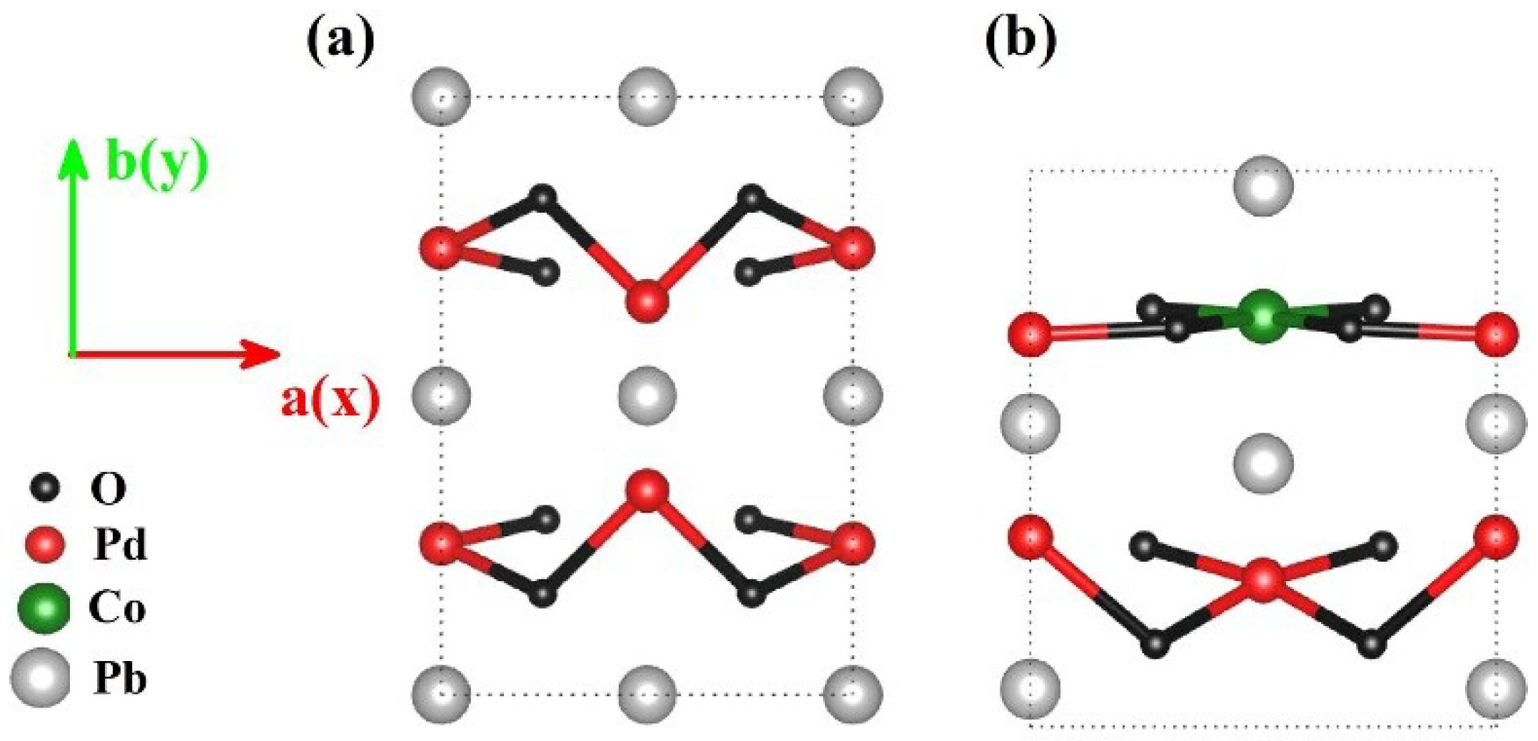
Figure 1 shows the relaxed crystal structures of PbPdO2 and PbPd0.75Co0.25O2 ultrathin slabs with (002) preferred orientation. As shown in Figure 1, the unstrained PbPdO2 and ultrathin slab revealed an in-plane symmetric configuration, maintaining the important properties of PbPdO2. After Co-doping, the symmetric configuration of PbPd0.75Co0.25O2 was broken. In comparison to the pristine PbPdO2, the broken-symmetry in PbPd0.75Co0.25O2 was expected to bring different physical properties. It should be noted that the anisotropy of PbPd0.75Co0.25O2 was greatly affected by the state of the Co-substitution. Moreover, its configurations were fairly complicated. Here, the configuration with the least number of atoms and only one Co doping atom was considered, as seen in Figure 1b. Specifically, this Co atom forms square planar bonding with the nearest-neighbor four O atoms, which plays an important role on the electrical properties of PbPd0.75Co0.25O2.
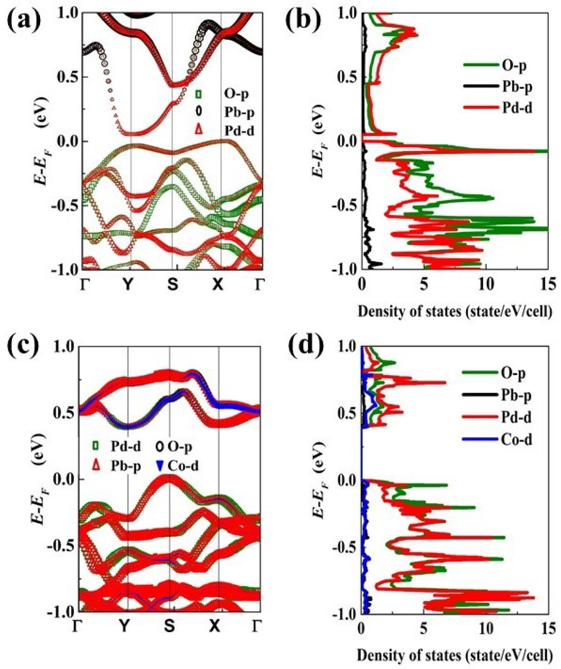
Figure 2a–d shows the calculated electronic structures and the partial densities of states of Pb, Pd, O, and Co in PbPdO2 and PbPd0.75Co0.25O2 slabs, respectively. It was found that PbPdO2 exhibits intrinsic characteristics of narrow band gap (0.051 eV), which was much smaller than that (0.4 eV) of the PbPd0.75Co0.25O2 slab. In our previous experimental work, PbPdO2 with (002) preferred orientation was prepared, and its band gap was found to be close to zero [22]. It is suggested that the localized Co would be responsible for the large band gap of 0.35 eV for the PbPd0.75Co0.25O2 bulk material. Interestingly, our calculated results were consistent with the reported results [23]. The band gap of PbPdO2 slab was slightly larger than that reported in our previous calculated work because of the different full in-plane structure relaxation [14]. From the density of electronic states in Figure 2b,d, it is found that DOSs of the pristine and Co-doped PbPdO2 slabs at minimum of the conduction band and maximum of the valence band were mainly composed of 4d(Pd) and 2p(O) states. These results were similar to those found by many research groups [6,10]. In contrast, the PbPd0.75Co0.25O2 slab had more distinct contribution of hybridization of 2p(O)–4d(Pd) states, where a Co 3d state added modified energy to the DOS at the Fermi energy level.
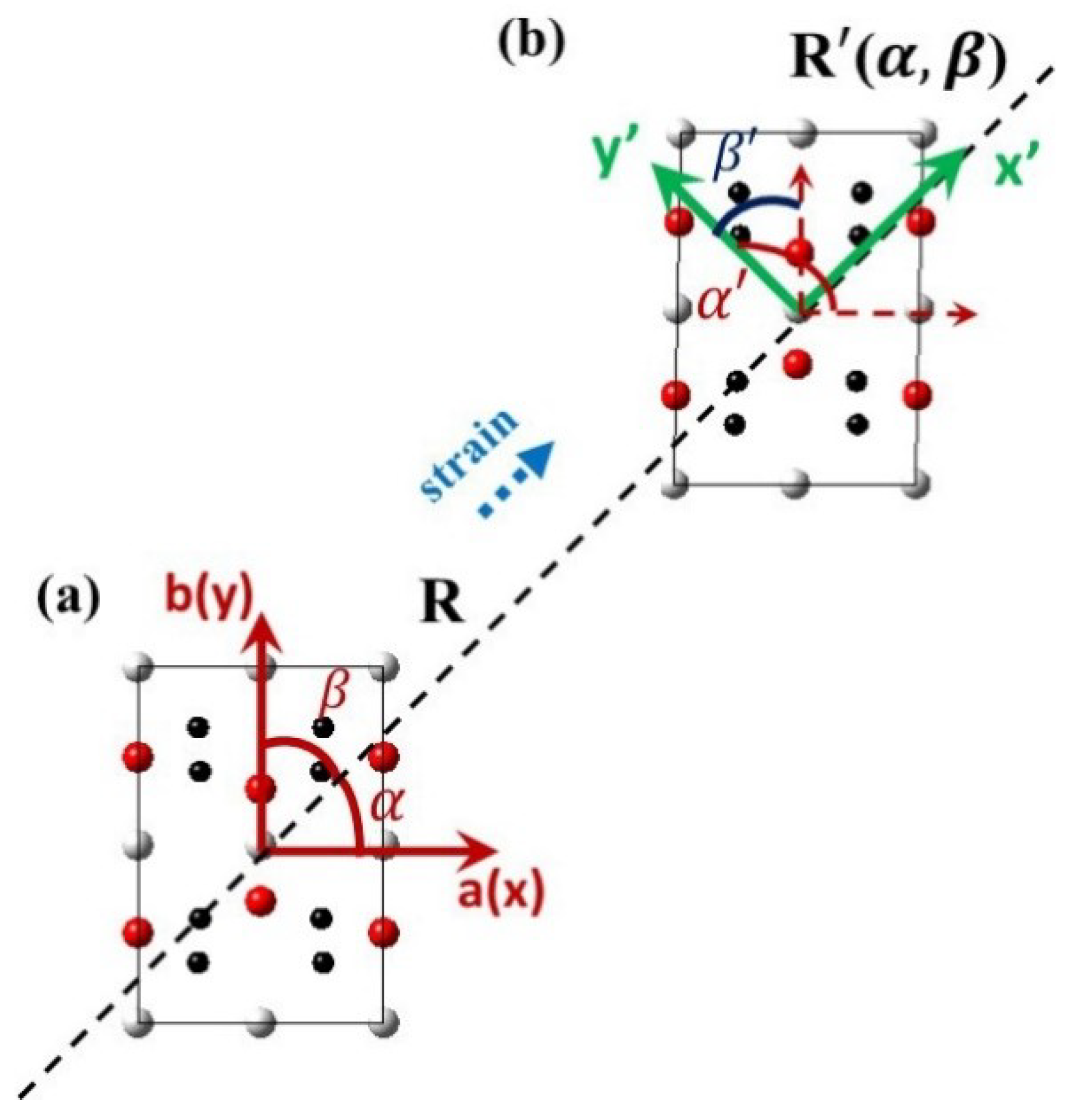
To gain insight into the potential mechanism of strain-induced electronic properties in PbPdO2-base composites, a plane-stress-strain model was set up. Figure 3a,b present the undeformed lattice and a deformed lattice with in-plane arbitrary uniaxial tensile strain (directional cosines ( cos α , cos β ) ), respectively. The strain-related components could be obtained based on the coordinate transformation method. Assuming uniaxial strain ε is along the x′ direction in an unprimed coordinate system x-y, the strain tensor elements in the primed coordinate system are given as follows,
[ ε x ε y γ x y ] = [ l 1 2 l 2 2 l 1 l 2 m 1 2 m 2 2 m 1 m 2 2 l 1 m 1 2 l 2 m 2 l 1 m 2 + l 2 m 1 ] [ ε x ε y γ x y ]
where ε x ( ε y ) and γ x y are normal (tensile or compressive) and shear strains, respectively [24]. The directional cosines are
l 1 = cos α ,   l 2 = cos α
m 1 = cos β ,   m 2 = cos β
where α , β , α , β are arbitrary directions in the x-y and x′-y′ coordinate system, as seen in Figure 3.
A deformation of the unit cell is created by changing the Bravais lattice vectors R of the undeformed unit cell to R′ using a strain matrix as follows:
R ( α , β ) = R [ 1 + ε x γ x y 0 γ x y 1 + ε y 0 0 0 1 ]
where R is the Bravais lattice vectors with strain, and R′ is the Bravais lattice vectors without strain, ε x ( ε y ) and γ x y ( γ y x ) are the normal (tensile or compressive) and shear strain-related components, respectively.
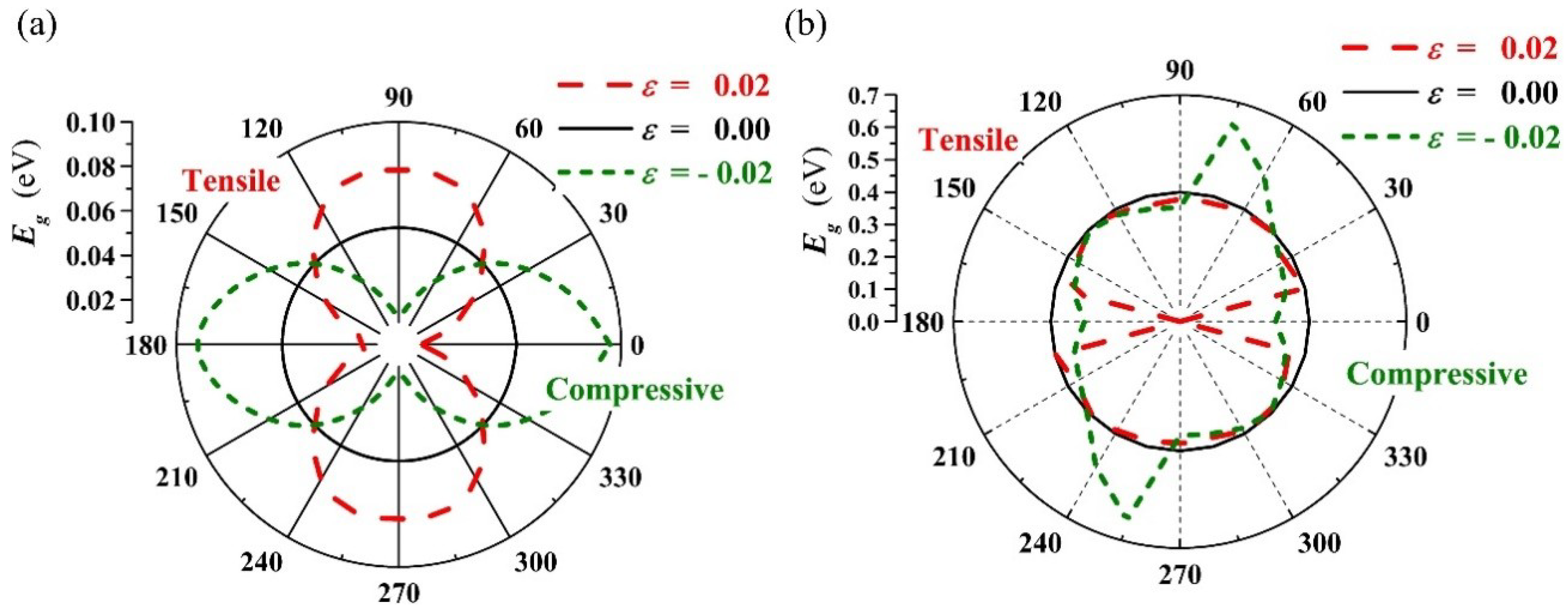
Figure 4a,b shows the orientation distribution curves of band gap E g with ε = −0.02, 0.00, 0.02 for the PbPdO2 and PbPd0.75Co0.25O2 slabs, respectively. It is clear that both slabs show a distinct anisotropy of gap with different strain. In Figure 4a, the PbPdO2 slab shows the symmetrical and peanut-like E g α curves, and having the largest and smallest band-gap values along the x axis ( α = 0 ) or y axis ( α = 90 ), respectively. In contrast, as shown in Figure 4b, the PbPd0.75Co0.25O2 slab has a maximum gap for the strain ε = −0.02 at about α = 75 and a minimum gap for the strain ε = 0.02 at about α = 0 .
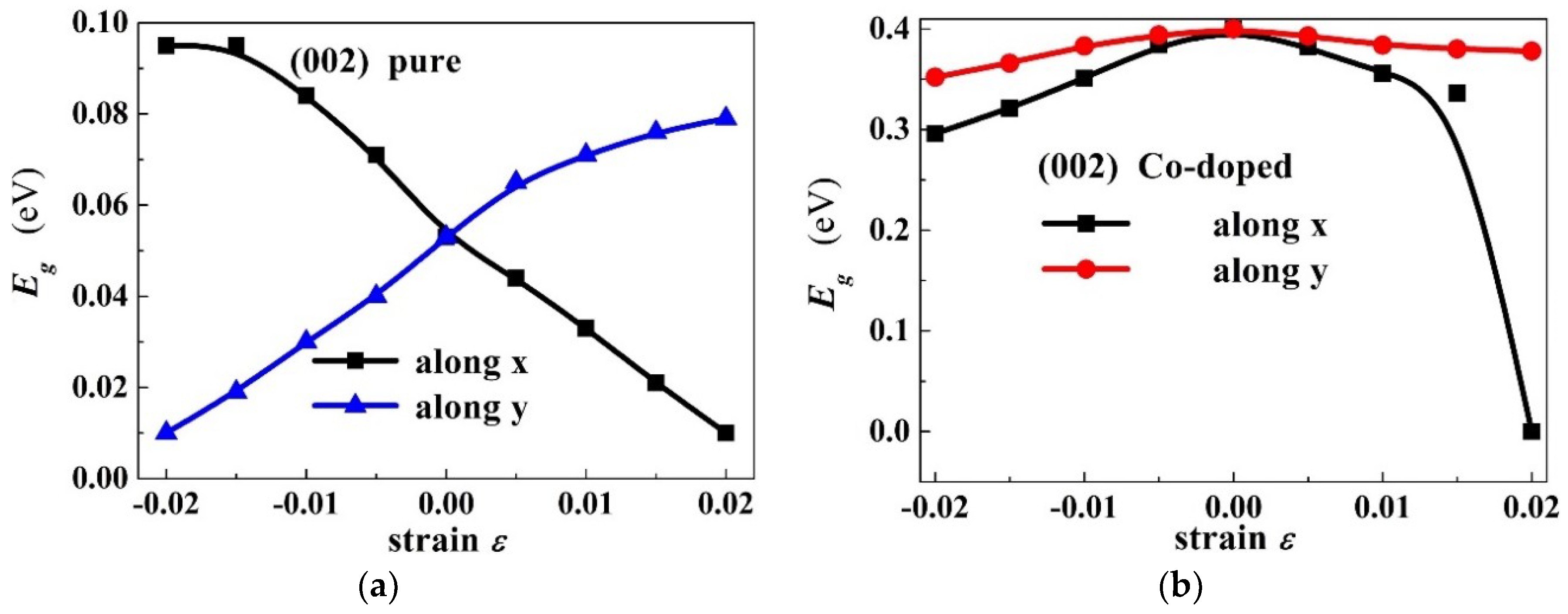
Figure 5a,b shows the band gap as a function of the strain for PbPdO2 and PbPd0.75Co0.25O2 along x axis ( α = 0 ) and y axis ( α = 90 ), respectively. As shown in Figure 5a, it is found that the band-gap value increases with increasing strain along the y-axis, whilst the band-gap value decreases with increasing strain along the x-axis. It is interesting that the band gap of the PbPdO2 slab would widen when a compressive stress is applied closely to the x-axis or a tensile stress is applied closely to the y-axis, as seen in Figure 4a. These calculated results can be explained according to the interaction of Pd–O bonding. It is expected that a compressive stress along the x-axis or tensile stress along the y-axis pulls O atoms apart from Pd atoms, which weakens the interaction of Pd and O. On the other hand, a tensile stress along the x-axis or compressive stress along the y-axis would push O atoms closely to Pd atoms and strengthen the interaction of Pd and O. As a result, the band gap is decreased. A similar result has also been reported in MoS2 and black phosphorus [25,26].
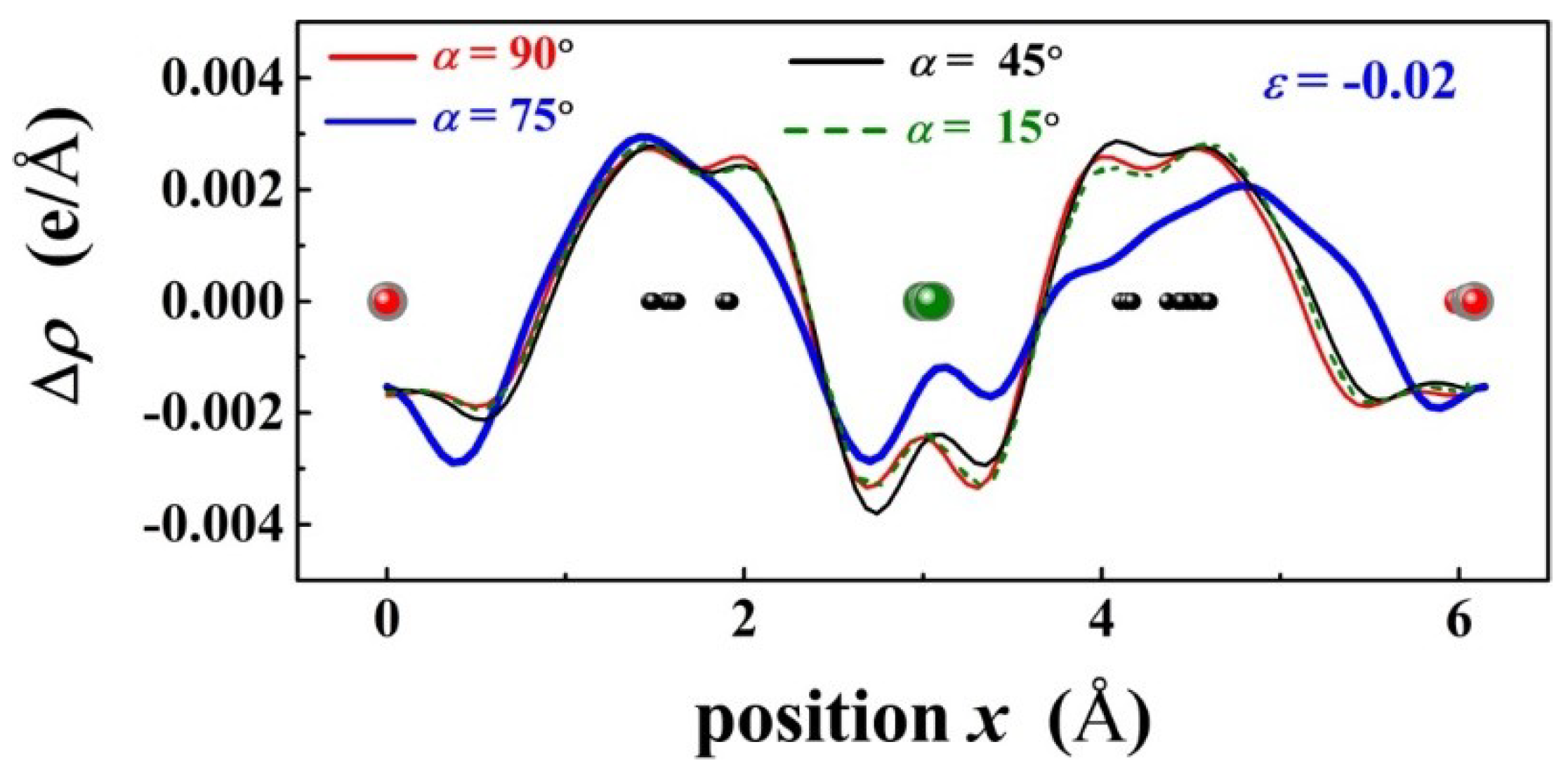
Figure 6 shows the plane averaged electron density difference Δρ of PbPd0.75Co0.25O2 projected along the x axis and under ε = −0.02, with α = 15°, 45°, 75°, and 90°, respectively. In comparison, it is found that p-d charge transfer Δρ between Co and O exhibits an evident change for α = 75°. Therefore, the band gap of PbPd0.75Co0.25O2 is expected to be changed significantly as the compressive stress direction is along a particular direction with α = 75°. 
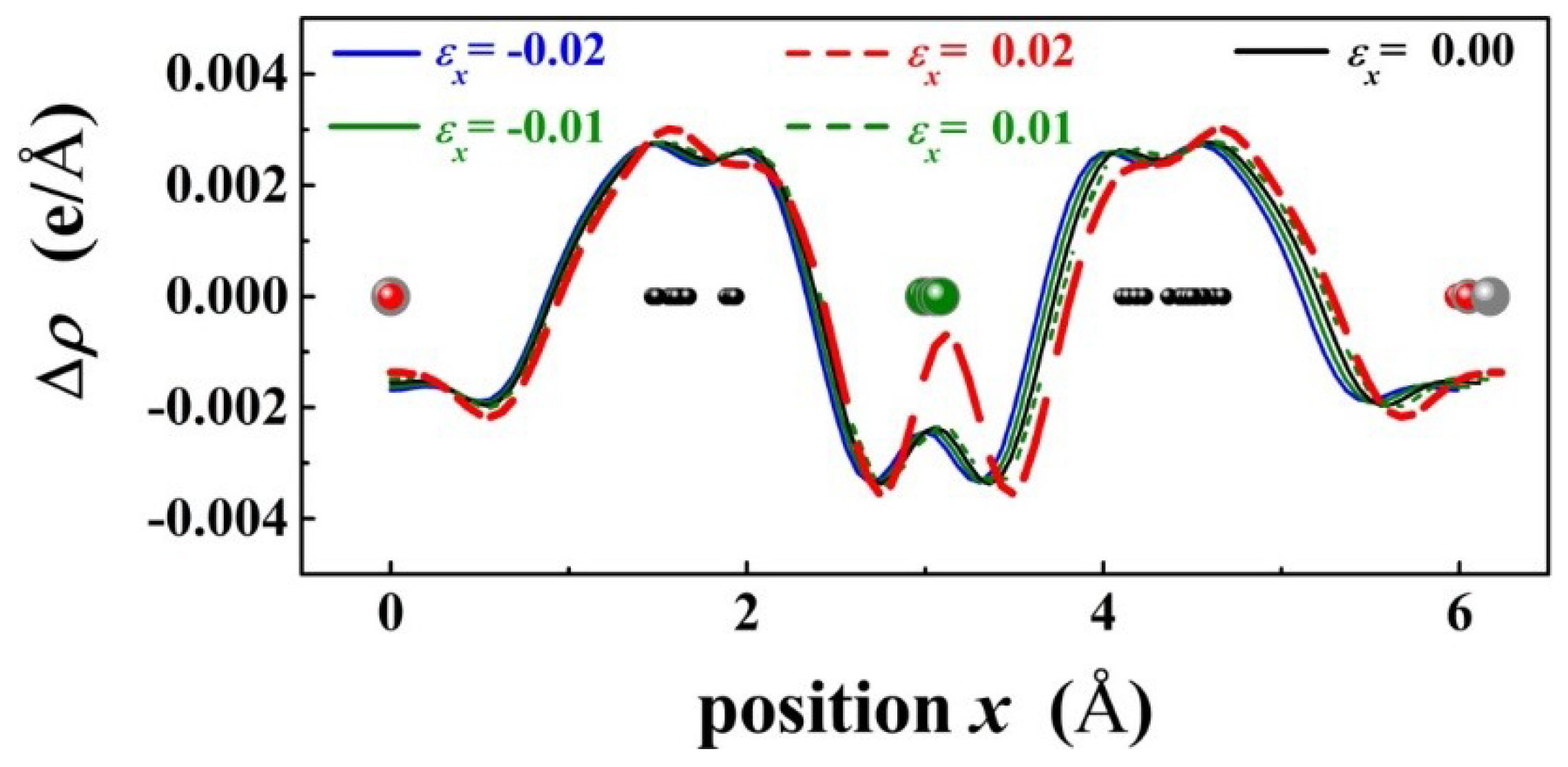
Figure 7 shows the plane averaged electron density difference Δ ρ of PbPd0.75Co0.25O2 projected along the x axis under ε x = −0.02, −0.01, 0.00, 0.01, 0.02, respectively. Based on spin-splitting theory, the minimum gap of the PbPd0.75Co0.25O2 slab with the strain ε x = 0.02 is strongly related to the variation of Δ ρ . From Figure 7, it is concluded that Co atom should act as the source of the localized magnetic moment, and the coupling between the p-state from O and d-state from Co could induce a strong exchange interaction (named as p-d exchange interaction) in PbPd0.75Co0.25O2. Moreover, the p-d exchange interaction was found to be nearly inversely proportional to the unit cell volume [27]. Therefore, p-d exchange interaction mediated by strain should be responsible for variation of the plane averaged electron density difference, leading to a clear change of the band gap.
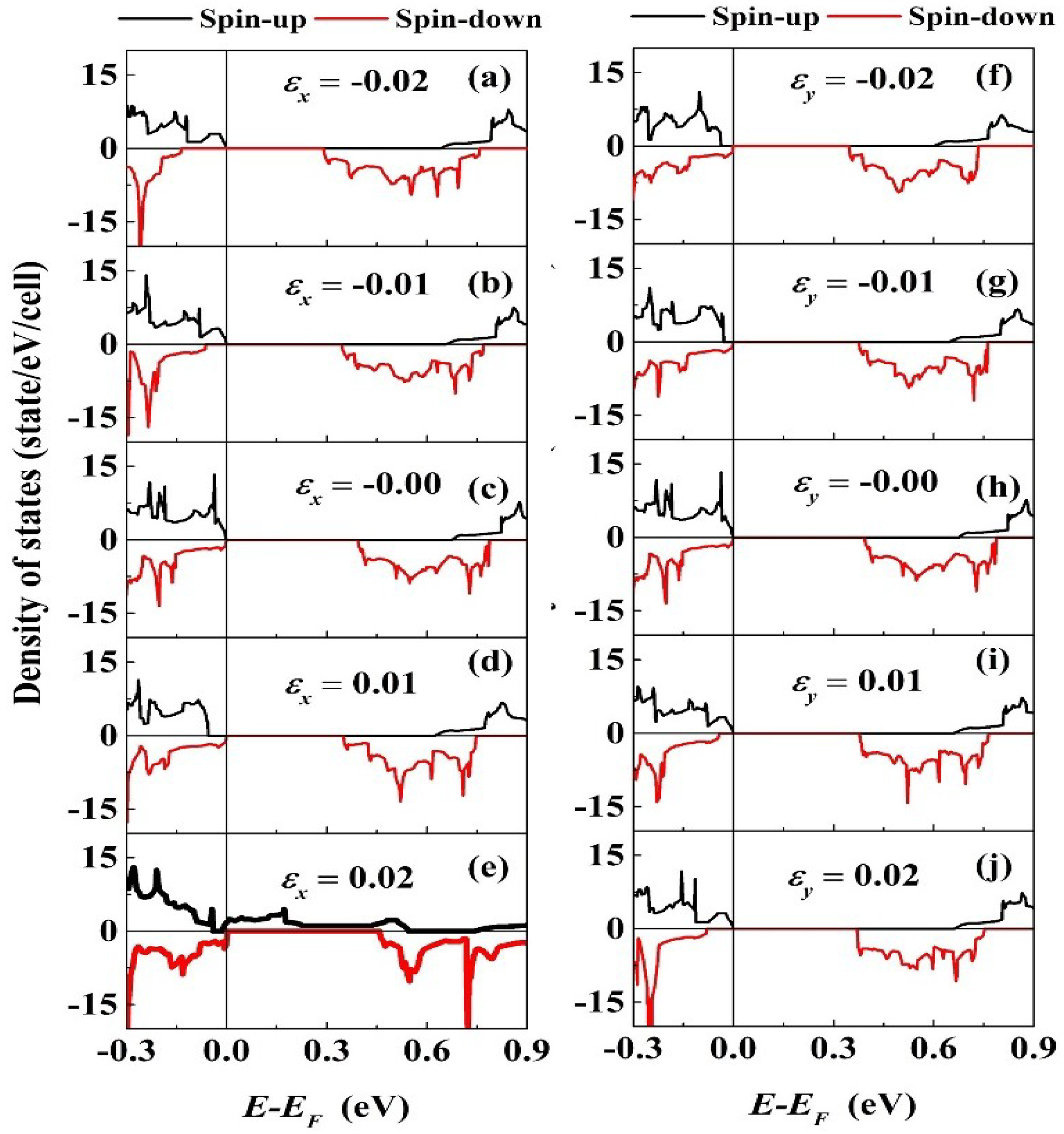
Figure 8 shows the spin polarized total density states of the PbPd0.75Co0.25O2 slab with different strain along the x and y-axes external uniaxial strain directions. From the figure, it is found that the spin-up and spin-down DOSs are asymmetric, which means the existence of magnetic moment. The magnetic properties in element doped PbPdO2 will be studied in subsequent research work. Interestingly, as shown in Figure 8e, the tensile strain with ε x = 0.02 leads to the zero-band gap structure. The strain gives rise to the evident left shift of the bottom of the conduction band in spin-down DOSs, which effectively modulates the band gap. When the strain is large enough, the top of the valence band and the bottom of the conduction band in spin-up and spin-down DOSs all shift with changing strain, which leads to clear modulation of the band gap. This interesting phenomenon is similar to the fact that the slight tensile strain results in the zero-band gap structure [4].
Unique electrical properties are highly desirable for practical application, and charge carrier concentration is a key parameter for the intrinsic semiconductor. For the intrinsic semiconductor, the charge charier concentration can be estimated as follows [28],
n T 3 / 2 exp [ E g 2 K B T ]
n ε / n 0 exp [ Δ E g 2 K B T ] = exp [ E g E g 0 2 K B T ]
where KB, Eg are the Boltzmann constant and band gap, respectively. In this paper, all the temperatures in carrier concentration were calculated at T = 100 K. As ε = 0, let n = n0; ε ≠ 0, let n = n ε .
Combined with the results presented in Figure 4a,b, the external strain dependence of charge carrier concentration ratio ( n ε / n 0 ) for PbPdO2 and PbPd0.75Co0.25O2 slabs were evaluated, respectively. 
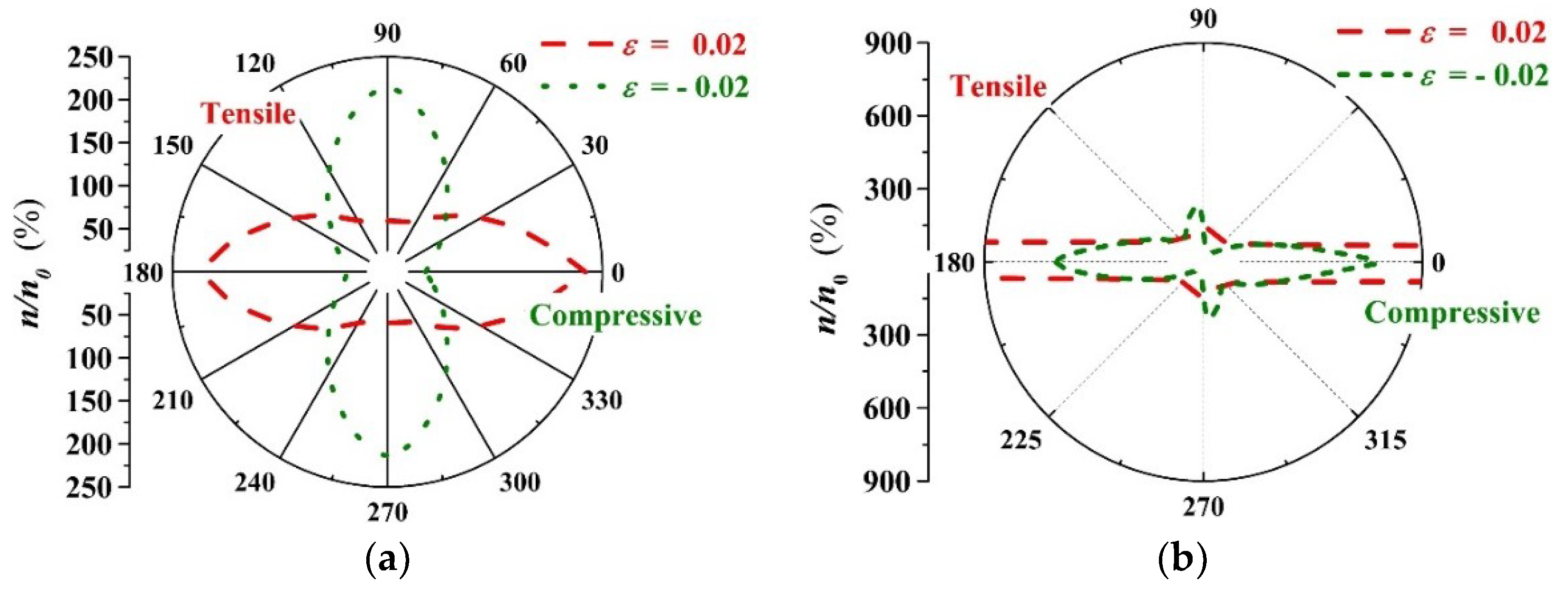
Figure 9a,b shows the orientation distribution curves of the intrinsic charge carrier concentration ratio n / n 0 for PbPdO2 and PbPd0.75Co0.25O2 slabs with ε = −0.02, −0.01, 0.00, 0.01, 0.02, respectively. Similar to the dependence of band gap E g on strain orientation, PbPd0.75Co0.25O2 exhibits more distinct anisotropy in carrier concentration with strain direction, especially along the x-axis. As shown in Figure 9a, the pristine PbPdO2 slab demonstrates the symmetrical and olive-like ( n ε / n 0 ) α curves, and having its largest and smallest band-gap values along the x-axis or y-axis, respectively. For the PbPd0.75Co0.25O2 slab, the carrier concentration is sensitive to the application direction of strain. When the compressive stress applies along a direction of 75° ( α 75 ) and x-axis, the remarkable variety in carrier concentration appears, as shown in Figure 9b. 
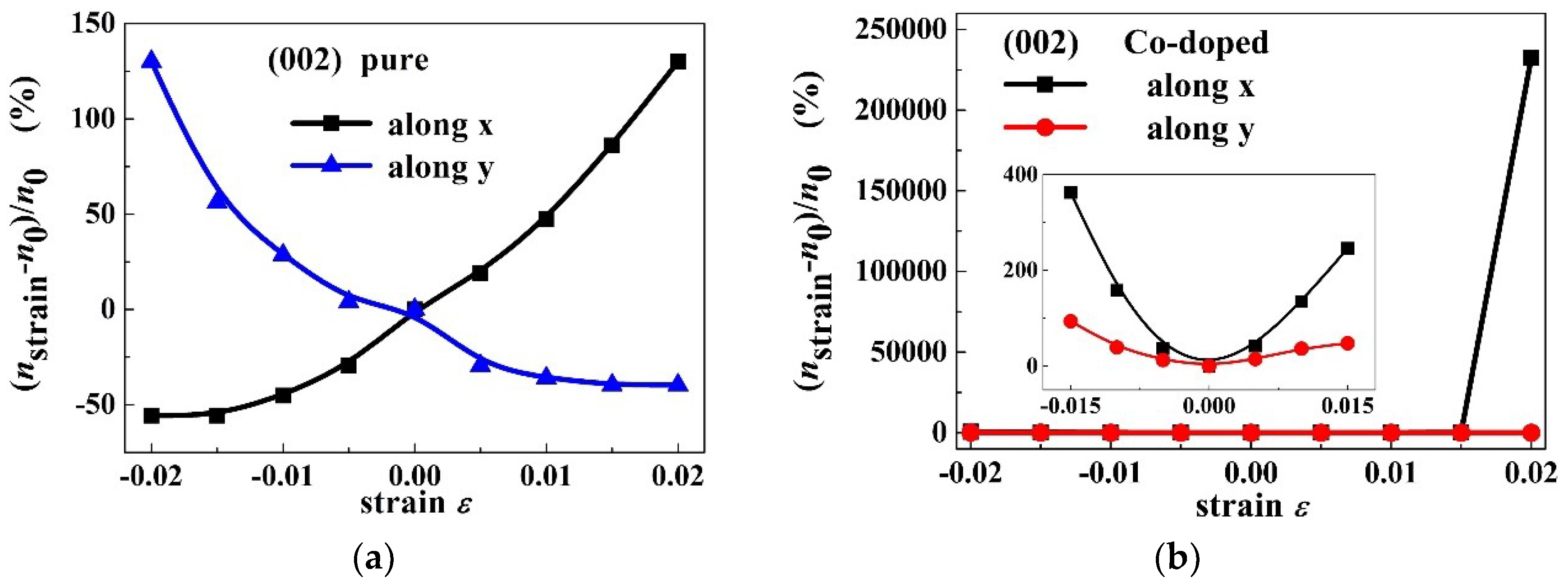
Figure 10c,d shows the intrinsic charge carrier concentration ratio ( n ε n 0 ) / n 0 as a function of strain for PbPdO2 and PbPd0.75Co0.25O2 slabs along the x and y-axes, respectively. For the PbPdO2 slab, the carrier concentration increases monotonically with increasing compressive stress, but decreasing with increasing tensile stress along the x-axis. On the contrary, the carrier concentration decreases with increasing compressive stress, while increasing with increasing tensile stress along the y-axis. In contrast, the carrier concentration of PbPd0.75Co0.25O2 slab increases with increasing compressive and tensile stresses along both the x and y-axes. As the compressive stress increases beyond 0.015 along the x-axis, carrier concentration of the PbPd0.75Co0.25O2 slab increases rapidly. It was found that the carrier concentration of PbPd0.75Co0.25O2 could sharply increase up to 5–6 orders of magnitude with the help of external strain with ε = 0.02. The calculated results suggest strongly that the element-doping PbPdO2 should become an important piezoresistance candidate material.
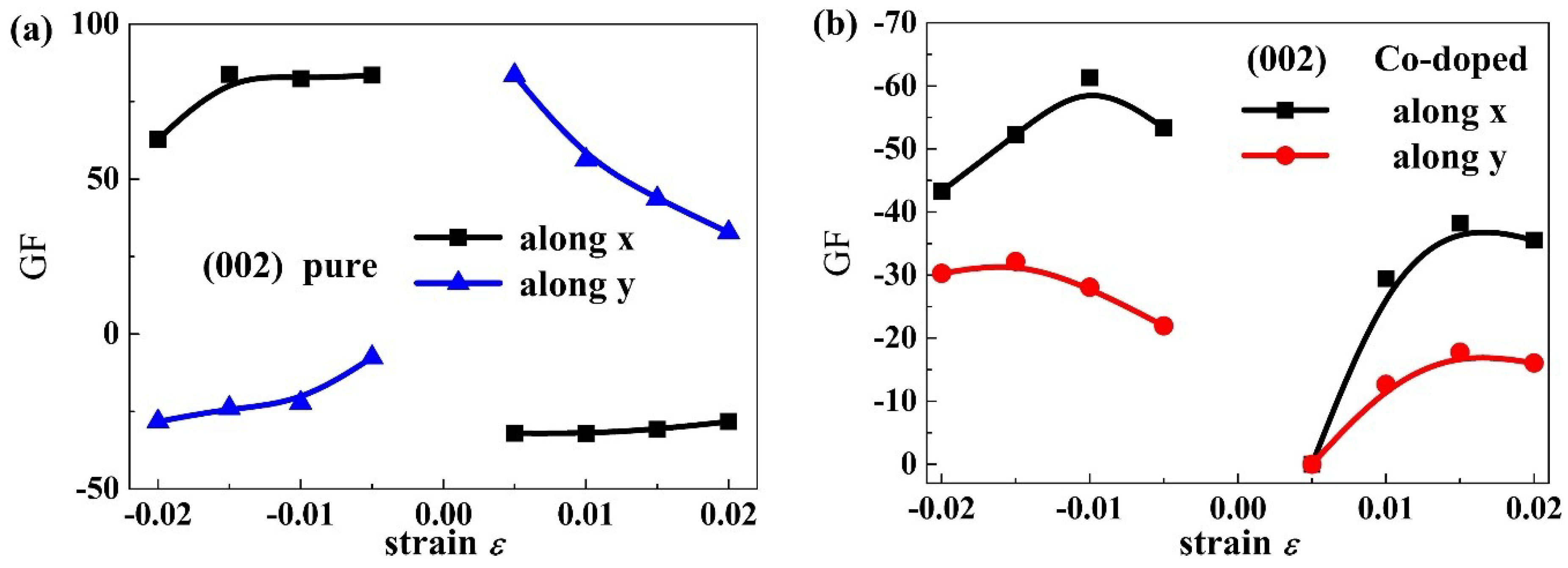
Figure 11 presents the strain dependence of gauge factor for the PbPdO2 and PbPd0.75Co0.25O2 slab along the x and y axes. Table 1 gives some typical gauge factor values. When the tensile strain is 0.02, the piezoresistive gauge factors for the PbPdO2 and PbPd0.75Co0.25O2 slab along the x-axis are calculated to be respectively 62.8 and −43.3, which is comparable to trilayer MoS2 and much higher than suspended-graphene-based strain sensor [29]. As Pd–O (Co–O) polar covalent bond is different from C–C bond, PbPdO2-based semiconductors can exhibit a higher piezoresistive gauge factor than graphene-based strain sensors. The predicted large gauge factors in our work implies that the element-doping PbPdO2 may have promising opportunities to be used as strain sensors.

4. Conclusions

Based on first-principles calculations, the electronic structures and electrical properties of PbPdO2 and PbPd0.75Co0.25O2 ultrathin slabs were systematically investigated. The calculated results indicated that the strain induces changes of band structure and carrier concentration in both slabs. Specifically, the carrier concentration of the PbPd0.75Co0.25O2 slab could be modulated with 5–6 orders externally induced strain, which renders the Co-doped pristine PbPdO2 phase a potentially promising piezoresistive material. Moreover, the above evident external strain modulation of the band gap and carrier concentration can be well explained by spin-splitting theory.

Author Contributions

Conceptualization, Y.Y., J.Z. and Z.H.; Methodology, Y.Y. and J.Z.; Formal Analysis, Y.Y., J.Z., K.Z. and Z.H.; Investigation, Y.Y., J.Z., G.X. and Z.H.; Writing—Original Draft Preparation, Y.Y., J.Z. and Z.H.; Writing—Review & Editing, Z.H.

Acknowledgements

This work was supported by the National Science Foundation of China (Nos. 61574037, 61804030, 11874113) and the Natural Science Foundations of Fujian Province of China (Nos. 2017J06001, 2016J05151, 2016J01011). G.X. would like to thank the support from Fujian Provincial College Funds for Distinguished Young Scientists of year 2015.

Conflicts of Interest

The authors declare no conflict of interest.

References

  1. Armand, M.; Tarascon, J.-M. Building better batteries. Nature 2008, 451, 652–657. [Google Scholar] [CrossRef] [PubMed]
  2. Ouardi, S.; Fecher, G.H.; Felser, C. Realization of spin gapless semiconductors: The Heusler compound Mn2CoAl. Phys. Rev. Lett. 2013, 110, 100401. [Google Scholar] [CrossRef] [PubMed]
  3. Bainsla, L.; Mallick, A.I.; Raja, M.M.; Coelho, A.A.; Nigam, A.K. Origin of spin gapless semiconductor behavior in CoFeCrGa: Theory and experiment. Phys. Rev. B 2015, 92, 045201. [Google Scholar] [CrossRef]
  4. Wang, X.L. Proposal for a new class of materials: Spin gapless semiconductors. Phys. Rev. Lett. 2008, 100, 156404. [Google Scholar] [CrossRef] [PubMed]
  5. Wang, X.L.; Peleckis, G.; Zhang, C.; Kimura, H.; Dou, S. Colossal electroresistance and giant magnetoresistance in doped PbPdO2 thin films. Adv. Mater. 2009, 21, 2196–2199. [Google Scholar] [CrossRef]
  6. Wang, X.L. Dirac spin-gapless semiconductors: promising platforms for massless and dissipationless spintronics and new (quantum) anomalous spin Hall effects. Nat. Sci. Rev. 2017, 4, 252–257. [Google Scholar] [CrossRef]
  7. Lee, K.S.; Choo, S.M.; Jung, M.-H. Magnetic versus nonmagnetic ion substitution effects in gapless semiconductor PbPdO2. Appl. Phys. Lett. 2015, 106, 072406. [Google Scholar] [CrossRef]
  8. Tang, F.L.; Liu, J.; Mei, C.; Huang, S.Y.; Song, T.T.; Su, H.L.; Lee, M.K.; Wu, Y.C.; Huang, J.C.A. Microstructure and magnetism of Co-doped PbPdO2 films with different grain sizes. RSC Adv. 2016, 6, 37522–37529. [Google Scholar] [CrossRef]
  9. Choo, S.M.; Lee, K.J.; Park, S.M.; Yoon, J.B.; Park, G.S.; You, C.-Y.; Jung, M.H. Crossover between weak anti-localization and weak localization by Co doping and annealing in gapless PbPdO2 and spin gapless Co-doped PbPdO2. Appl. Phys. Lett. 2014, 106, 172404. [Google Scholar] [CrossRef]
  10. Chen, S.W.; Huang, S.C.; Guo, G.Y.; Lee, J.M.; Chiang, S.; Chen, W.C.; Liang, Y.C.; Lu, K.T.; Chen, J.M. Gapless band structure of PbPdO2: A combined first principles calculation and experimental study. Appl. Phys. Lett. 2011, 99, 012103. [Google Scholar] [CrossRef]
  11. Srivastava, P.; Nagare, B.J.; Kanhere, D.G.; Sen, P. Electronic structure of the spin gapless material Co-doped PbPdO2. J. Appl. Phys. 2013, 114, 103709. [Google Scholar] [CrossRef]
  12. Liu, J.; Mei, C.; Chuang, P.Y.; Song, T.T.; Tang, F.L.; Su, H.L.; Huang, J.C.A.; Wu, Y.C. Effect of Fe doping on the magnetic properties of PbPdO2 nanograin film fabricated by sol-gel method. Ceram. Int. 2016, 42, 15762–15766. [Google Scholar] [CrossRef]
  13. Kim, D.H.; Hwang, J.; Lee, E.; Lee, K.J.; Choo, S.M.; Jung, M.H.; Baik, J.; Shin, H.J.; Kim, B.K.; Min, B.I.; et al. Valence states and electronic structures of Co and Mn substituted spin gapless semiconductor PbPdO2. Appl. Phys. Lett. 2014, 104, 022411. [Google Scholar] [CrossRef]
  14. Yang, Y.M.; Zhong, K.H.; Xu, G.G.; Zhang, J.-M.; Huang, Z.G. Electronic structure and its external electric field modulation of PbPdO2 ultrathin slabs with (002) and (211) preferred orientations. Sci. Rep. 2017, 7, 6898. [Google Scholar] [CrossRef] [PubMed]
  15. Peng, X.; Wei, Q.; Copple, A. Strain-engineered direct-indirect band gap transition and its mechanism in two-dimensional phosphorene. Phys. Rev. B 2014, 90, 085402. [Google Scholar] [CrossRef]
  16. Kanda, Y. Piezoresistance effect of silicon. Sens. Actuators A Phys. 1991, 28, 83–91. [Google Scholar] [CrossRef]
  17. Wu, W.; Wang, L.; Li, Y.; Zhang, F.; Lin, L.; Niu, S.; Chenet, D.; Zhang, X.; Hao, Y.; Heinz, T.F.; et al. Piezoelectricity of single-atomic-layer MoS2 for energy conversion and piezotronics. Nature 2014, 514, 470–474. [Google Scholar] [CrossRef] [PubMed]
  18. Manzeli, S.; Allain, A.; Ghadimi, A.; Kis, A. Piezoresistivity and strain-induced band gap tuning in atomically thin MoS2. Nano Lett. 2015, 15, 5330–5335. [Google Scholar] [CrossRef] [PubMed]
  19. Kresse, G.; Furthmüller, J. Efficiency of ab-initio total energy calculations for metals and semiconductors using a plane-wave basis set. Comput. Mater. Sci. 1996, 6, 15–50. [Google Scholar] [CrossRef]
  20. Kresse, G.; Furthmüller, J. Self-interaction correction to density functional approximation for many electron systems. Phys. Rev. B 1996, 54, 11169–11186. [Google Scholar] [CrossRef]
  21. Perdew, J.P.; Burke, K.; Ernzerhof, M. Generalized gradient approximation made simple. Phys. Rev. Lett. 1996, 77, 3865–3868. [Google Scholar] [CrossRef] [PubMed]
  22. Chen, X.; Chen, Y.; Yang, Y.M.; Jia, H.; Zhang, J.M.; Chen, S.Y.; Huang, Z.G. The structure and electrical properties of PbPdO2 thin films with preferred orientation prepared by PLD. Ceram. Int. 2017, 43, 10428–10433. [Google Scholar] [CrossRef]
  23. Chen, S.W.; Huang, S.C.; Guo, G.Y.; Lee, J.M.; Chiang, S.; Chen, W.C.; Liang, Y.C.; Lu, K.T.; Chen, J.M. A combined first principle calculations and experimental study on the spin-polarized band structure of Co-doped PbPdO2. Appl. Phys. Lett. 2012, 101, 222104. [Google Scholar] [CrossRef]
  24. Chen, H.; Huang, P.; Guo, D.; Xie, G.X. Anisotropic mechanical properties of black phosphorus nanoribbons. J. Phys. Chem. C 2016, 120, 29491–29497. [Google Scholar] [CrossRef]
  25. Li, C.; Fan, B.; Li, W.-Y.; Wen, L.-W.; Liu, Y.T.; Sheng, W.K.; Yin, Y. Band gap engineering of monolayer MoS2 under strain: A DFT study. J. Korean Phys. Soc. 2015, 66, 1789–1793. [Google Scholar] [CrossRef]
  26. Rafael, R.; Andrés, C.-G.; Emmanuele, C.; Francisco, G. Strain engineering in semiconducting two-dimensional crystals. J. Phys. Condens. Matter 2015, 27, 313201. [Google Scholar] [Green Version]
  27. Dietl, T.; Ohno, H.; Matsukura, F. Hole-mediated ferromagnetism in tetrahedrally coordinated semiconductors. Phys. Rev. B 2001, 63, 195205. [Google Scholar] [CrossRef] [Green Version]
  28. Grosso, G.; Parravicini, G.P. Solid State Physics, 2nd ed.; Academic Press: Amsterdam, The Netherlands, 2014; pp. 577–582. ISBN 978-0-120385030-0. [Google Scholar]
  29. Smith, A.D.; Niklaus, F.; Paussa, A.; Vaziri, S.; Fischer, A.C.; Sterner, M.; Forsberg, F.; Delin, A.; Esseni, D.; Palestri, P.; et al. Electromechanical piezoresistive sensing in suspended graphene membranes. Nano Lett. 2013, 13, 3237. [Google Scholar] [CrossRef] [PubMed]
Figure 1. Top view of atomic structures in ab plane, (a) PbPdO2, and (b) PbPd0.75Co0.25O2 with (002) orientation.
Materials 11 02002 g001
Figure 2. (a) electronic structures, and (b) orbital-resolved partial density of states (DOS) of (002) orientation PbPdO2 slab; (c) electronic structures, and (d) orbital-resolved partial DOS of (211) orientation PbPd0.75Co0.25O2 slab. The abscissa in (a,c) is the path of high symmetry points in Brillouin zone.
Materials 11 02002 g002
Figure 3. Diagram for (a) an undeformed lattice, (b) a deformed lattice with in-plane arbitrary uniaxial tensile strain (directional cosines ( cos α , cos β ) ).
Materials 11 02002 g003
Figure 4. The orientation distribution curves of band gap E g for (a) PbPdO2, and (b) PbPd0.75Co0.25O2 with ε = −0.02, 0.00, 0.02.
Materials 11 02002 g004
Figure 5. Band gap E g as a function of strain for (a) PbPdO2, and (b) PbPd0.75Co0.25O2 along x-axis (called x) and b-axis (called y).
Materials 11 02002 g005
Figure 6. The plane averaged electron density difference Δ ρ of PbPd0.75Co0.25O2 projected along the x axis and under ε = −0.02, with α = 15°, 45°, 75°, and 90°, respectively.
Materials 11 02002 g006
Figure 7. The plane averaged electron density difference Δ ρ of PbPd0.75Co0.25O2 under ε x = −0.02, −0.01, 0.00, 0.01, 0.02, where the projection of Δ ρ was along the x axis.
Materials 11 02002 g007
Figure 8. The spin polarized total density states of the PbPd0.75Co0.25O2 slab with different strain ε x ( ε y ) : (ae) along the x-axis, and (fj) along the y-axis external uniaxial strain directions.
Materials 11 02002 g008
Figure 9. The orientation distribution curves of intrinsic charge carrier concentration ratio n / n 0 for (a) PbPdO2, and (b) PbPd0.75Co0.25O2 with ε = −0.02 and 0.02.
Materials 11 02002 g009
Figure 10. The intrinsic charge carrier concentration ratio ( n ε n 0 ) / n 0 as a function of strain for (a) PbPdO2, and (b) PbPd0.75Co0.25O2 along the a-axis (called x) and b-axis (called y) with ε = −0.02 and 0.02. The inset shows a magnification curve with strain ranges from −0.015 to 0.015.
Materials 11 02002 g010
Figure 11. The piezoresistive gauge factor as a function of strain for (a) PbPdO2, and (b) PbPd0.75Co0.25O2 along the x and y axes.
Materials 11 02002 g011
Table 1. Some typical gauge factors of PbPdO2 and PbPd0.75Co0.25O2 along the x and y axes.
Typical Gauge FactorsPbPdO2 SlabPbPd0.75Co0.25O2 Slab
Direction
xyxy
ε−0.020.02−0.020.02−0.020.02−0.020.02
GF62.8−28.3−28.332.8−43.3−35.5−30.3−16.1

