Article

Chemical and Morphological Characterization of Magnetron Sputtered at Different Bias Voltages Cr-Al-C Coatings

1
Chair of Physical Metallurgy and Materials Technology, Brandenburg Technical University, Cottbus 03046, Germany
2
Boreskov Institute of Catalysis SB RAS, Novosibirsk 630090, Russia
3
Department of Material Science, Welding and Strength of Material, Faculty of Mechanical Engineering, Wroclaw University of Science and Technology, Wrocław 50370, Poland
4
Chair of Experimental Physics II/Materials Science, Brandenburg Technical University, Cottbus 03046, Germany
*
Author to whom correspondence should be addressed.
Materials 2017, 10(2), 156; https://doi.org/10.3390/ma10020156
Submission received: 21 December 2016 / Accepted: 3 February 2017 / Published: 10 February 2017

Abstract

:
MAX phases (M = transition metal, A = A-group element, and X = C/N) are of special interest because they possess a unique combination of the advantages of both metals and ceramics. Most attention is attracted to the ternary carbide Cr2AlC because of its excellent high-temperature oxidation, as well as hot corrosion resistance. Despite lots of publications, up to now the influence of bias voltage on the chemical bonding structure, surface morphology, and mechanical properties of the film is still not well understood. In the current study, Cr-Al-C films were deposited on silicon wafers (100) and Inconel 718 super alloy by dc magnetron sputtering with different substrate bias voltages and investigated using Scanning Electron Microscopy (SEM), X-ray Photoelectron Spectroscopy (XPS), X-ray Diffraction (XRD), Atomic Force Microscopy (AFM), and nanoindentation. Transmission Electron Microscopy (TEM) was used to analyze the correlation between the growth of the films and the coating microstructure. The XPS results confirm the presence of Cr2AlC MAX phase due to a negative shift of 0.6–0.9 eV of the Al2p to pure aluminum carbide peak. The XRD results reveal the presence of Cr2AlC MAX Phase and carbide phases, as well as intermetallic AlCr2. The film thickness decreases from 8.95 to 6.98 µm with increasing bias voltage. The coatings deposited at 90 V exhibit the lowest roughness (33 nm) and granular size (76 nm) combined with the highest hardness (15.9 GPa). The ratio of Al carbide to carbide-like carbon state changes from 0.12 to 0.22 and correlates with the mechanical properties of the coatings. TEM confirms the columnar structure, with a nanocrystalline substructure, of the films.

1. Introduction

MAX phases are ternary carbides and/or nitrides with the composition form Mn + 1AXn, where n is 1, 2 or 3; M is an early transition metal; A is an A-group element from the periodic table of elements; and X is carbon or nitrogen [1]. Since their scientific discovery in the 1960s by Jeitschko et al. [2,3], MAX phases have gained significant attention due to their combination of the merits of metals and ceramics [4,5]. They exhibit high stiffness [6,7], easy machinability [5], self-healing behavior [8], chemical- [9,10], oxidation- [11,12] and hot corrosion resistance [13,14].
MAX-phase films have been synthesized using different chemical (CVD) and physical (PVD) methods. In 2002, Palmquist et al. [15] deposited Ti3SiC2 onto single-crystal substrates by Physical Vapour Deposition (PVD). Since then different PVD methods have been used for the deposition of MAX phases, including magnetron sputtering.
Nowadays, the ternary carbide Cr2AlC has a great potential for industrial application due to excellent high-temperature oxidation resistance and hot corrosion resistance due to the formation of a protective Al2O3 layer [16,17,18,19]. Cr2AlC film has been successfully deposited onto silicon wafers [20], single crystalline oxide [21,22], steel [23], Ni-based superalloy [17,24], and Ti alloy [25]. Cr2AlC has been produced using magnetron sputtering, either by sputtering from elemental targets [26] or compound targets [23]. Field et al. [27] deposited Cr2AlC coatings using direct current magnetron sputtering (DCMS) and high power impulse magnetron sputtering (HiPIMS).
It is well known that the microstructure and properties of PVD coatings strongly depend on deposition parameters such as deposition temperature, sputtering power, substrate bias, etc. [28]. The deposition temperature needed for the formation of Cr2AlC thin films was discussed in different works [13,23,24]. Walter et al. [23] reported the formation of Cr2AlC from a compound target at a substrate temperature of 450 °C. Li et al. [24] produced Cr2AlC coatings by magnetron sputtering from a bulk Cr2AlC target at a substrate temperature range of 370–500 °C. However, Abdulkadhim et al. [13] reported that a higher temperature is required for Cr2AlC formation. In a previous publication by Naveed et al. [17], the influence of sputtering power on growth and mechanical properties of Cr2AlC was already discussed. It was found that preferential coating growth orientation changes and a slight increase in hardness occurs with increasing sputtering power.
However, despite many studies on magnetron sputtered Cr2AlC films [13,17,23,24,26,27,29,30,31], up to now the effect of bias voltage on the chemical bonding structure, surface morphology, and mechanical properties of film is still not well understood.
The purpose of this work is to study the influence of bias voltage on the properties of Cr-Al-C coatings deposited onto IN718 and silicon wafers (100). The influence of the substrate bias voltage on the coating characteristics, such as chemical bonding structure, surface morphology, and roughness, was investigated using X-ray photoelectron spectroscopy (XPS) and atomic force microscopy (AFM). Mechanical properties were examined by means of nanoindentation. Transmission electron microscopy was used to analyze the correlation between the growth of the films and the coating microstructure.

2. Experimental Section

Cr-Al-C coatings were deposited on (100) silicon wafers and Inconel 718 super alloy (NiCr19Fe19Nb5Mo3), finding its application in gas turbines [32]. Inconel 718 specimens were polished using SiC paper up to 2400 grade, further cleaned ultrasonically, and dried in air. The coating deposition was performed in a CC800/9 industrial coater from CemeCon AG (Würselen, Germany). Prior to deposition, the specimens were etched under a vacuum at a pressure of 350 MPa for 30 min. Direct current magnetron sputtering was used with a compound target (88 × 500 mm2) with a Cr:Al:C composition of 2:1:1 supplied by CemeCon AG. The sputtering process was performed in static mode. The deposition temperature was 550 °C because this temperature is shown in the literature as the lowest temperature, where Cr2AlC formation is ensured [13]. The distance between the target and the substrate was 70 mm. Further details of the deposition process parameters for Cr-Al-C coatings are given in Table 1.
A scanning electron microscope (SEM, TESCAN Mira, Prague, Czech Republic) was used to investigate the growth of the films on (100) Si wafers. Crystallographic phases and XRD patterns of the films were identified using a D8 Discover X-ray diffractometer (Bruker AXS, Karlsruhe, Germany) with a grazing incidence X-ray diffraction (GIXRD) method at a low incident angle of 9° with a Cu Kα source (λ = 0.15406 nm) operating at 40 kV and 40 mA.
An ES300 KRATOS spectrometer (Kratos Analytical, Manchester, UK), equipped with an X-ray tube with twin Mg and Al anodes, was used for the XPS studies. Prior to the installation of the samples into the spectrometer, their surfaces were cleaned by washing them several times in pure ethanol. Photoelectron spectra were acquired after evacuation to an ultra-high vacuum (UHV, 5 × 10⁻⁹ mbar). The electron analyzer was calibrated against Au4f7/2 (84.0 eV) and Cu2p2/3 (932.7 eV) photoelectron line positions obtained from Ar+ ion cleaned metallic surfaces of copper and gold. Non-monochromated Mg Kα-radiation was used for sample analysis. Due to the conductivity of the samples, the XP-spectra were presented without calibration.
The spectra processing was performed using XPS-Calc software (Boreskov Institute of catalysis, Novosibirsk, Russia) [33]. Doniach-Sunjic asymmetric lineshape was used for the description of the components related to carbide phase in Cr2p, Al2p, and C1s spectra due to the conductive character of this phase. The sample coated at 90 V bias voltage was characterized by XPS after evacuation to UHV and after Ar+ ion etching at 1 keV and 20 mA for 30, 60, 90 and 120 min. The samples prepared with other bias voltages were characterized after 120 min ion etching.
The surface morphology of the films was analyzed by AFM (“Smena” microscope by NT-MDT, Zelenograd, Russia) operating in contact mode with cantilever NSG 11 Pt (NT-MDT). The AFM observation was supported by TEM methods, using a Hitachi H-800 transmission electron microscope (Hitachi High-Technologies Corp., Tokyo, Japan) with an accelerating voltage of 150 kV. Cross-sectional samples were prepared using the focused ion beam (FIB) technique. The selected area diffraction patterns were analyzed using software developed in the Electron Microscopy Lab at Wroclaw University of Technology. In order to determine the mechanical properties (hardness and E-Modulus) of the coatings, nanoindentation tests were carried out using a UNAT nanoindenter (ASMEC GmbH, Radeberg, Germany) with a Berkovich Indenter (three-face pyramid diamond) by means of the Quasi Continuous Stiffness Method (QCSM). A load of 15 mN was used, hence the penetration depth did not exceed 10% of the total coating thickness in order to neglect the substrate effect [17,32]. The load-displacement curves were analyzed using the Oliver Pharr method [34]. For each sample, the mean value of twenty single measurements was calculated.

3. Results and Discussion

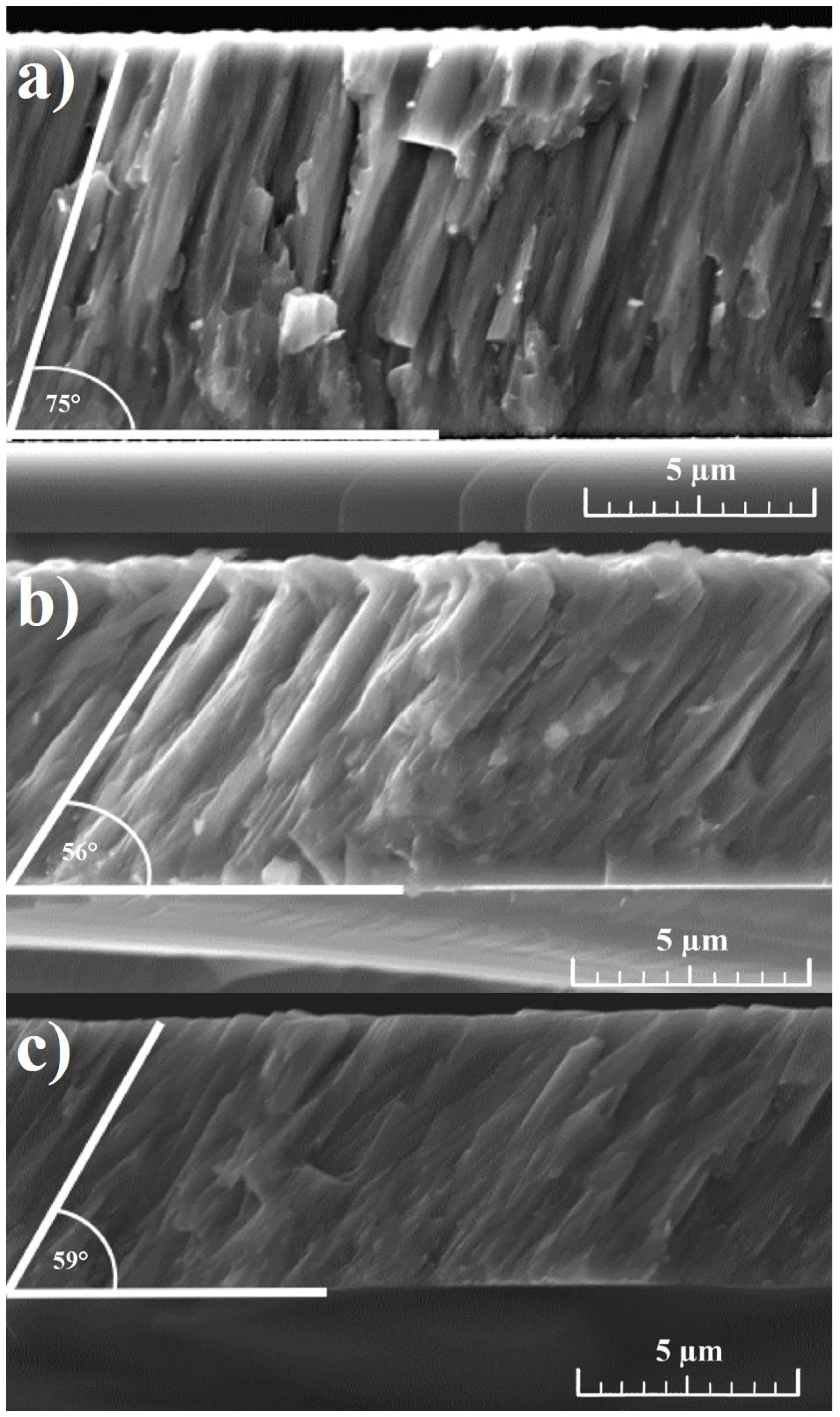
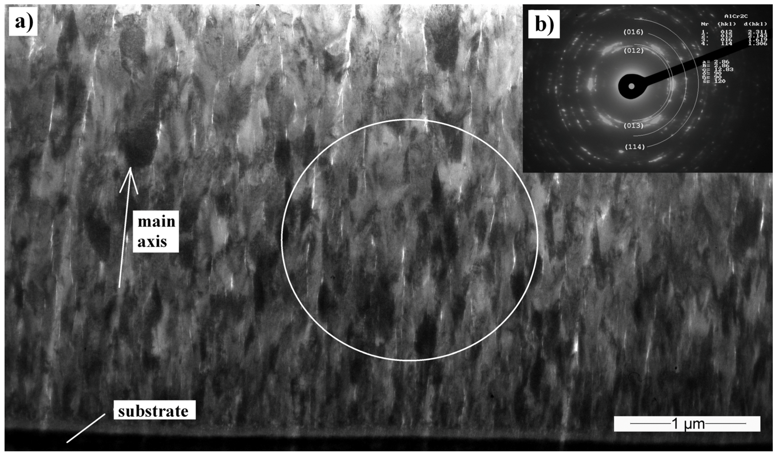
3.1. Scanning Electron Microscopy
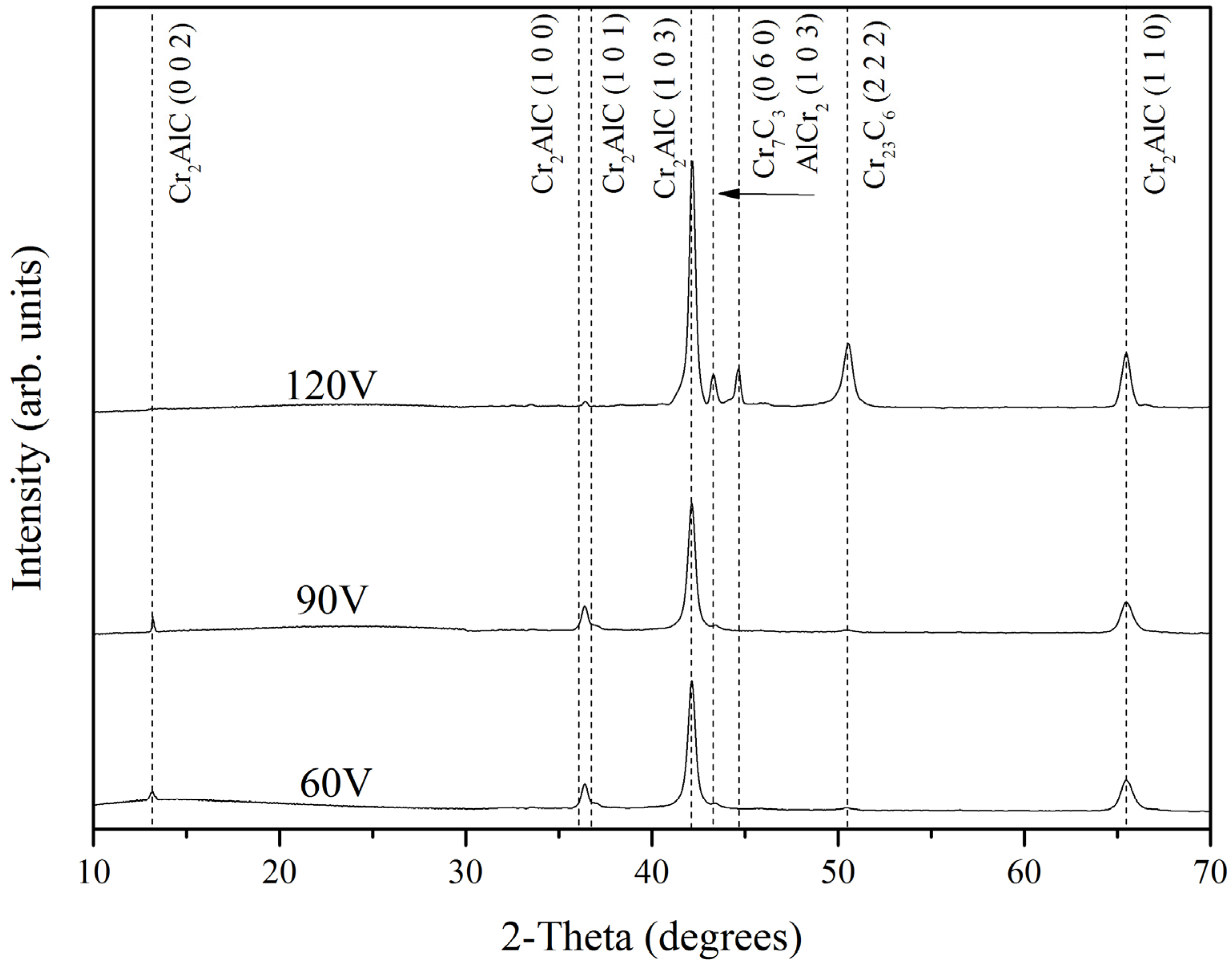
The coating growth was analyzed by means of SEM, as shown in Figure 1. The cross-sectional view of the coating deposited at 60 V shows a collection of dense columns grown on the substrate with an angle of nearly 75° with respect to the substrate. Surface analysis indicates a feathery structure showing apparent columns of various diameters. According to the Thornton model, this structure could be attributed to Zone-T [35]. With the increase of substrate voltage, a clear change in column growth can be seen. Different growth angles of approximately 56° and 59° can be observed for Cr-Al-C during growth at 90 V and 120 V, respectively. Naveed et al. [17] observed similar columnar structures with certain column orientations relating to the substrate at sputtering powers up to 2.5 kW.

3.2. XRD

Representative X-ray diffraction (XRD) patterns of the deposited Cr-Al-C coatings obtained by GIXRD are given in Figure 2. In the range 10°–70°, there are two super lattice reflections, (002) and (101), corresponding to the ordered Cr2AlC MAX phase [29,36]. At around 13.3°, (002) weak reflection for coatings at 60 and 90 V was found, identifying the presence of the MAX phase [29]. The XRD patterns corresponding to 60 V and 90 V are very similar. These two coatings show the Cr2AlC (103) as the dominant orientation and a small amount of (100/101) of the same phase. The XRD pattern of 120 V is different to the others. The Cr2AlC (103) peak is stronger for 120 V, which can be related to larger grains, higher crystallinity, or more MAX phase. This is in good correlation with the results of Field et al. [27], who showed for DCMS and HiPIMS deposited coatings that Cr2AlC (103) reflection was the highest. Furthermore, the coating deposited at 120 V displays the presence of Cr7C3, AlCr2, and Cr23C6 peaks.

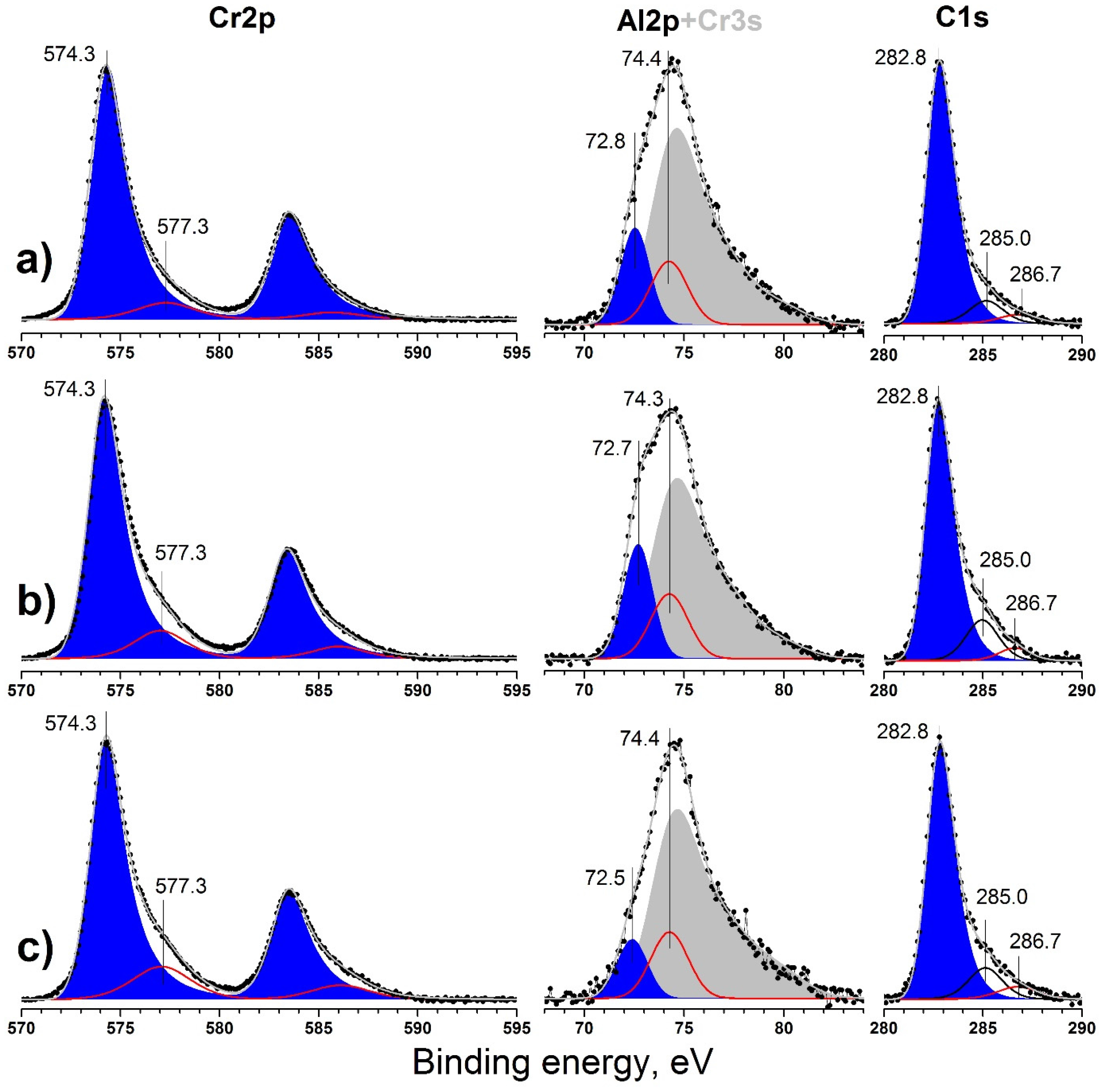
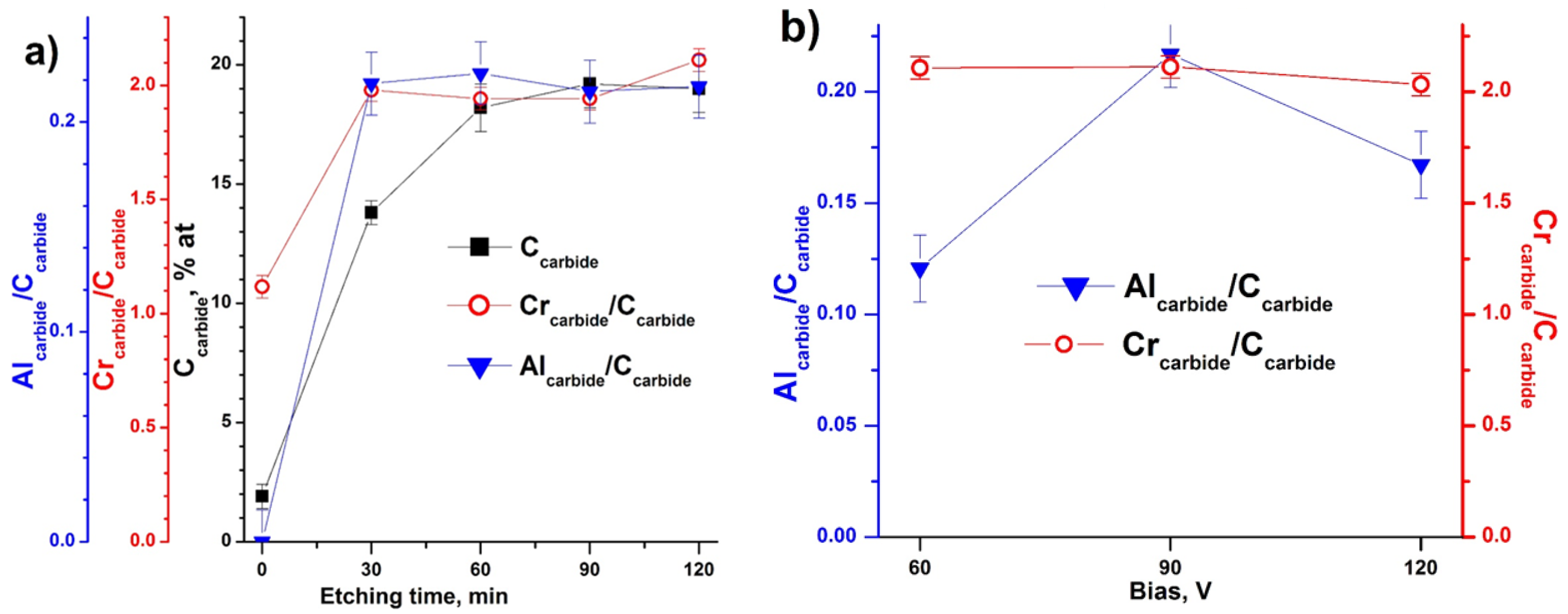
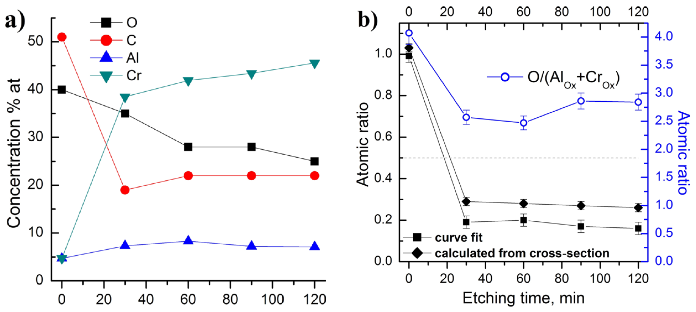
3.3. X-ray Photoelectron Spectroscopy

XPS analysis allows information to be obtained about the chemical structure of the elements on the surface of samples. The samples were exposed to air prior to the XPS measurements. Therefore, the initial surface of all samples was oxidized and strongly contaminated. Survey spectra revealed Cr, Al, C and O peaks, and a carbon content of more than 50% was measured on the surface (Figure 3a). Cr as well as Al concentrations on the untreated surface were observed at about 5%. The coating deposited at 90 V was measured after 30, 60, 90 and 120 min of argon ion etching (Ar+ etching rate: 2 Å/min) in order to study the chemical composition of the surface layers. Figure 3b shows the atomic concentration of the elements versus etching time.
Argon etching led to a decrease of C and O and to an increase of Cr and Al concentration due to the removal of contaminated and oxidized layers on the surface. The composition reached a constant value after 60–90 min of argon etching. It is noticed that after 120 min of etching, oxygen still remained at approximately 20%. It is assumed that this amount of oxygen was incorporated into the coatings during deposition. The analysis of the deposition process reveals that the most likely source of oxygen contamination may be residual oxygen in the deposition chamber. The oxygen incorporation in the structure of M2AlC phases is well known [31,37]; however in our case the concentration is higher than expected.
Note that the initial surface was depleted with chromium; the Al/Cr ratio was about 1. The chromium concentration sharply increased in the first 30 min of etching and slightly changed during further etching, while the aluminum concentration remained almost constant. Thus, the inner layers (6–24 nm depth) were depleted with aluminum. The upper limit of the Al/Cr ratio (Figure 3b) was estimated to be less than 0.35, which was substantially lower than the specified value of 0.5. The origin of such a low Al/Cr ratio obtained from XPS is discussed below (see the description of Al2p + Cr3s lines presented on Figure 4). Thus, all samples were substantially depleted with aluminum in the subsurface layers. The amount of oxygen on the cleaned surfaces increased with the decrease in substrate bias from 120 to 60 V.
Typical high resolution XPS spectra of Cr2p, Al2p, and C1s core levels of coatings prepared at different bias voltages are presented on Figure 4a–c. Etching of the surface for 120 min led to almost complete removal of oxidized Cr3+ species and carbon contaminants.
The carbon valence state represented mainly by the peak at 282.8 is typical for carbide-like carbon in all cases, i.e., typical for the Cr–C bond [38]. Higher than typical values for Al4C3 (282.2 eV) indicate the absence of a discrete aluminum carbide phase [39]. Only minor additional components were observed at 285.0 and 286.6 eV, which corresponds to elementary carbon (C–C bonds) and oxidized carbon species (C–O). They were probably formed due to the decomposition of carbide phases into pure elements under ion beam influence (Ar ion damage [40]) and the subsequent removal of the decomposition products [41,42]. Thus, a steady-state concentration of elementary carbon species was observed.
Chromium was represented by two states with binding energies; (BE) = 574.3 and 577.3 eV. Minor components at 577.3 eV corresponding to Cr2O3 were observed [43]. The main asymmetric component at 574.3 eV corresponds to chromium in carbide phase [44] or in metallic Cr [38]. Similar XPS results were presented by Zamulaeva et al. for Cr2AlC prepared using pulsed electrospark deposition (PED) [45]. Furthermore, both peaks are situated in the same position for all coatings, and no chemical shift could be discerned.
The minor Cr3s photoelectron line overlaps with the Al2p main photoelectron line of aluminum. The estimation of Al2p contribution to this spectrum is possible via two ways. Theoretical Al2p contribution can be estimated using the Cr2p photoelectron spectra and Scofield cross-sections [46] of the 3s and 2p core-levels of chromium for the calculation of the Cr3s line intensity. Thus, the theoretical Al/Cr ratio could be obtained. The most probable experimental Al/Cr ratio can be estimated via the curve of best fit of the experimental spectrum from the total areas of the peaks at 72.7 and 74.4 eV in the Al2p + Cr3s on Figure 4 using binding energy and the shape of Cr3s taken from [43,47,48]. The Al/Cr ratios obtained each way are presented in Figure 3b. The Al/Cr ratio was calculated to be about 0.3 using the theoretical approach and about 0.2 using curve fitting of the experimental spectra, which were both lower than the specified value 0.5.
Aluminum was much more oxidized compared to chromium due to its more metallic chemical properties, as obvious from the intensity of the peak at 74.3–74.4 corresponding to Al2O3 [49,50]. The accuracy of the Al2p + Cr3s photoelectron line fitting is confirmed by the quotient of the total oxygen amount and the oxidized Al + Cr species (doublet peak at 577.3 eV in Cr2p and peak at 74.4 in Al2p + Cr3s), which is close to 3 and presented in Figure 5b. Thus, these peaks in the Cr2p and Al2p + Cr3s lines correspond to Cr2O3 and Al2O3, respectively.
The peak at 72.8–72.5 eV formally corresponds to metallic aluminum, which has a binding energy of about 72.6–72.8 eV [39,51]. Aluminum carbide is characterized by a higher binding energy of Al2p core level 73.4 eV [39]. Thus, taking into account the rather high reactivity of aluminum towards carbon [39], we attribute this state to Cr2AlC. The negative shift 0.6–0.9 eV relative to pure aluminum carbide can be explained with more metallic Al–C bonds in Cr2AlC phase compared to Al4C3. Zhang et al. observed a similar negative shift of the Al2p core level for Ti2AlN phase compared to pure AlN. Thus, such a shift could be used as indicator of MAX phase formation [51,52]. In the current study, the XPS results could confirm the formation of a Cr2AlC MAX phase, and these results are in good agreement with the XRD measurements.
The Cr and Al carbide states standardized on carbide-like C reached a constant value after 30 min of ion etching, while total carbide-like C concentration reached a constant value only after 60 min of ion etching (Figure 5a). Thus, despite the removal of carbon contaminants and oxidized species, the carbide phase composition is constant in the topmost ~24 nm; however, this phase is deplete of aluminum and corresponds to Cr2:Al0.25:C1 stoichiometry in the case of the Cr-Al-C coating at 90 V (Figure 5a). Taking into account the oxidation of the surfaces with oxygen traces during ion etching, the initial “non-oxidized” surface composition was estimated to correspond to the Cr2:Al0.6–0.7:C1 stoichiometry under this assumption.
Moreover, the Cr carbide to carbide-like C state ratio was very stable, independent of the bias voltage (Figure 5b), and equal to 2.03–2.1, while the Al non-oxidized carbide state to carbide-like C state varied from 0.12 to 0.22.

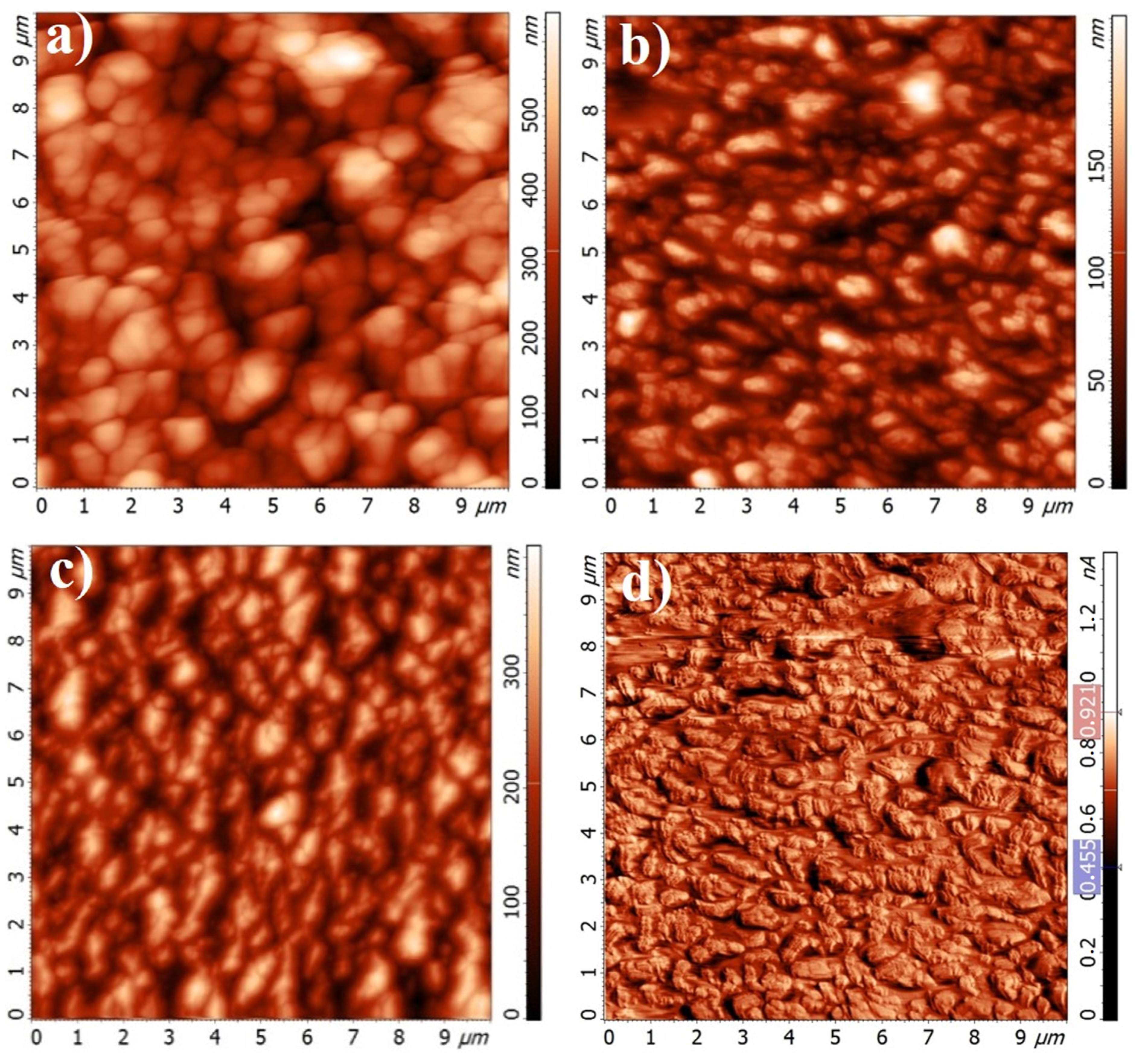
3.4. Atomic Force Microscopy

AFM gives information about the morphological properties of films. The main characteristics of Cr-Al-C coatings like thickness, surface roughness, and granular size are listed in Table 2. Thickness, as a function of bias voltage, shows an inverse relationship with the bias. The film thickness reduces from 8.95 to 6.98 µm, which can be related to the notable sputtering off of the film (re-sputtering) [53,54].
During increasing bias voltage, the incident ion energy rises and, therefore, more atoms from the growing coatings will be re-sputtered [55,56]. These results are in good correlation with the literature [53,57,58,59]. However, Jiang et al. showed that, at a low bias voltage (till 50 V), the thickness can increase with rising bias until the ion current density is saturated [54].
The surface morphologies of the coated silicon substrates were examined by the AFM method and shown in Figure 6. All films have a granular structure with visible agglomerated grains. The Cr-Al-C coating deposited at 60 V exhibits the morphology with the highest RMS (root-mean-square). As the substrate bias changes from 60 to 90 V, the structure changes from irregular to rectangular particulates with random alignment and the roughness sharply decreases to 33 nm, indicating a surface-smoothing phenomenon.
The lateral force map for the sample deposited at 90 V with the pronounced superstructure of the films is presented in Figure 6d. A step-line structure is evident, and its edges are visible. At 120 V, the film became again rougher with a roughness of about 60 nm (Figure 6c). The increase in roughness with rising bias voltage can be explained by higher ion energy [60,61].
The average granular size was obtained using atomic force microscopy. Similar to the roughness, the granular size significantly decreases as the bias increases from 60 V to 90 V and then rises during a further increase to 120 V.
Reduction of granular size can also be related to a modification of the superficial morphology by argon ion bombardment, increasing the energy associated with the atoms on the substrate surface and/or the growing coating surface [62]. In addition, Lee et al. [63] reported that applied DC bias may cause an increase in the point defects in the film’s structure, increasing compressive residual stress and reducing the grain size. However, as mentioned above, when the bias voltage increases, the ion energy increases, resulting in higher adatom mobility. High energy promotes diffusion as well as grain boundary migration that might cause increasing granular size [60,64]. Similar results were also reported by Gangopadhyay et al. [53] and Zhang et al. [65]. As available from Table 2, the first increase in bias voltage results in a decreasing granular size, while a further increase in bias voltage leads to an increase in granular size. Therefore, in the literature, both effects were discussed contradictorily. Thus, a superposition of different effects takes place. The problem of whether higher adatom mobility, higher ion energy, and more defects result in smaller or larger granular size has still not been solved [53,65].

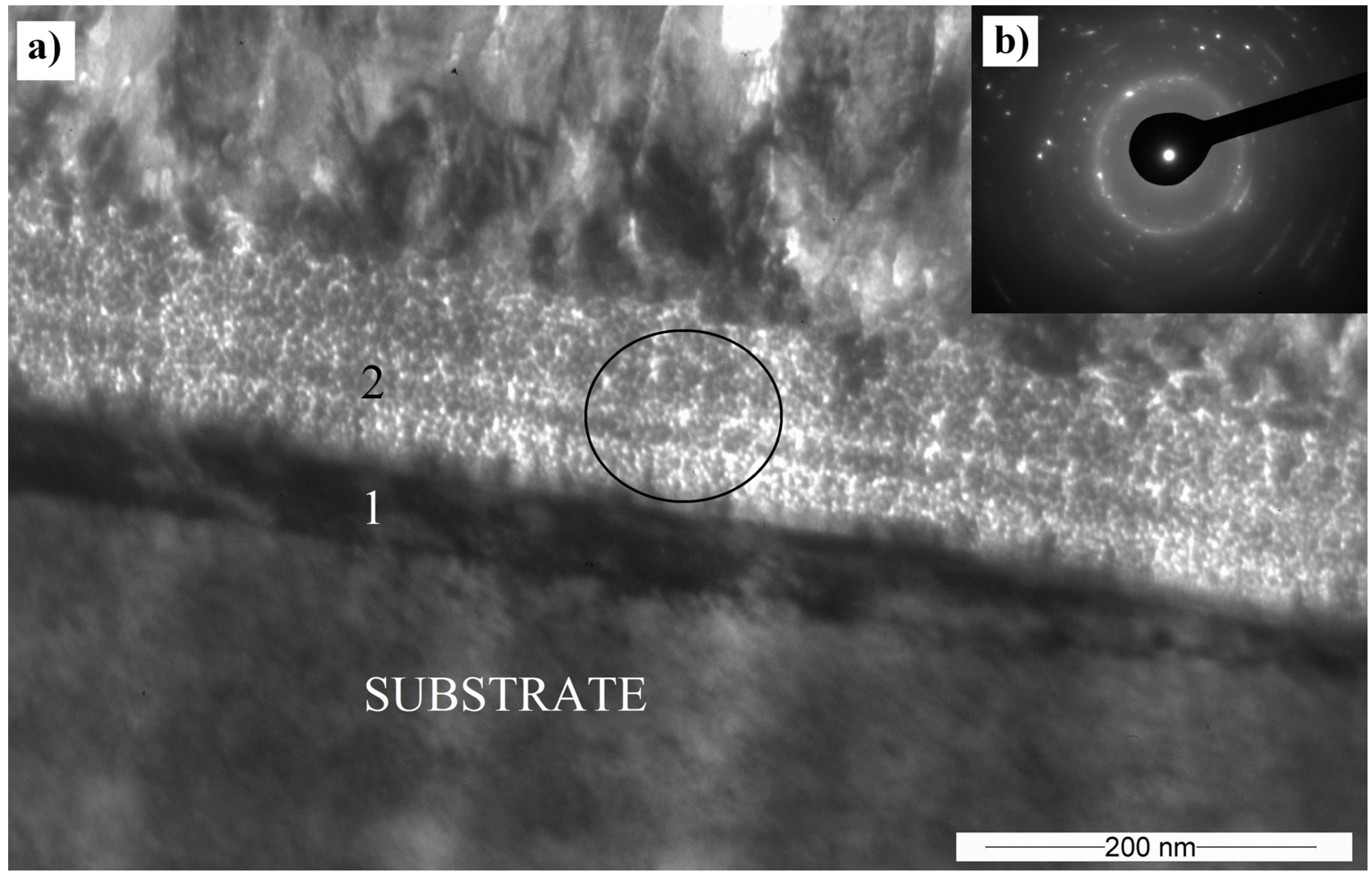
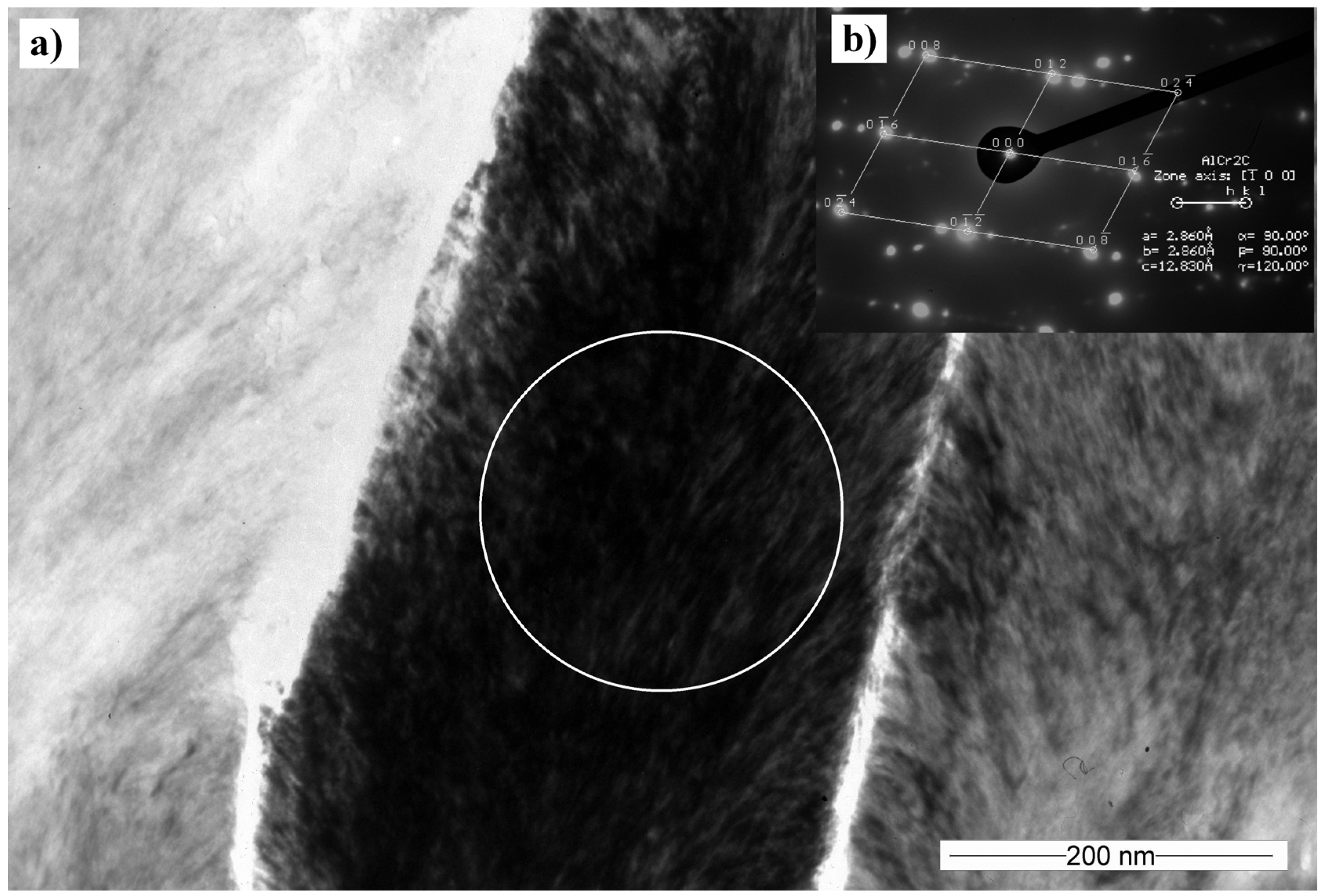
3.5. Transmission Electron Microscopy

Cross-sectional TEM samples of the Cr2AlC film deposited at 90 V were analyzed by means of TEM to understand the coating growth. The coating layer exhibits a columnar polycrystalline growth structure consisting of 120–250 nm width columns (Figure 7a). The selective area electron diffraction taken from a 3-µm diameter circle shows a textured coating with preferential columnar orientation. Cr2AlC phase was recognized and the Cr2AlC planes (012) (d012 = 0, 2311 nm), (013) (d013 = 0, 2143 nm), (016) (d016 = 0, 1619 nm), and (008) (d008 = 0, 1346 nm) were detected. The coating is visibly textured. The angle measurement of the most varied diffraction spots in the same interplanar distance showed that most of the grains are oriented in ±15° angle to the main growth axis.
The substrate-coating interface region shows the presence of two layers marked with the numbers 1 and 2 in Figure 8. An amorphous or nanocrystalline layer marked with number 1 has about a 50–60 nm thickness. Between the amorphous region and the columnar crystal, a 100–120 nm nanocrystalline layer exists. In this region, the beam is strongly dispersed but has not created a circular polycrystalline pattern. It is possible to observe individual crystalline reflections, but the pattern has the attributes of an amorphous or nanocrystalline structure.
The diffraction taken in a single grain confirms the presence of Cr2AlC phase (Figure 9a). The selected area electron diffraction reveals blurred fuzzy streaks and extra diffraction spots along the direction [016] (Figure 9b). They can be caused by the formation of a superlattice structure inside the Cr2AlC grain, ordered stacking faults, or another long-period ordered crystal arrangement. This theory corresponds to the bright-field image, showing an oriented substructure inside the Cr2AlC grain (Figure 9a). Further results of the TEM analysis of the crystal growth will be published in the near future.

3.6. Nanoindentation

The hardness (H), elastic modulus (E), and the H/E and H3/E2 ratios of the coatings were obtained using a nanoindenter. The results had shown that the mechanical properties of the coating were influenced by the bias values (Table 3). The hardness and E-modulus values rapidly increased from 8.8 to 15.8 GPa and from 223.4 to 307.7 GPa, respectively, when bias rose from 60 V to 90 V. By further increasing the bias voltage up to 120 V, H and E were decreased. The H/E and H3/E2 values possessed maximums of 0.042 and 0.052, obtained at a bias voltage of 90 V. High H/E and H3/E2 values mean larger elastic strain to failure and higher fracture toughness [66]. The high hardness at 90 V is probably due to the reduction in granular size caused by the ionic bombardment [62]. Consequently, this enhancement of the mechanical properties with the increase in the applied bias voltage is caused by a blockage for the displacement of the cracks, and thus the energy necessary for the motion of cracks through the coating increases [67]. As previously reported in the literature, an increase in substrate bias raises the level of compressive residual stresses due to an increasing number of impinging ions onto the substrate as well as higher ion current density [68,69]. The XPS results show a change in the ratio of Al carbide state to carbide-like C state, determining the mechanical properties of the films. This statement needs further investigation and more detailed analysis. The nanoindentation results are consistent with the previous work of the authors [17], with hardness values in the range between 11 and 14 GPa at various sputtering powers as well as with further investigations about Cr2AlC [6,25]. Schneider et al. [6] measured the hardness value of Cr2AlC as 13 ± 2 GPa. Zamulaeva et al. [25] reported a hardness of 15.4 GPa and an elastic modulus of 288 GPa for coatings produced using pulsed electrospark deposition (PED). These hardness values are rather low in comparison to the nanoindentation data of Ti2AlC [70] and Ti3AlC2 [71] and are similar to V2AlC coatings [72,73] prepared using magnetron sputtering. Furthermore, the hardness values presented above are significantly higher than those for bulk MAX phases, which are typically 2–4 GPa [1]. This increase could be explained by the Hall-Petch’s effect [74], wherein the strength of materials is inversely proportional to the square of the crystalline size before a decreased threshold value. Due to the rapid cooling during PVD vapor condensation, the coatings developed nanocrystalline structure, which can be attributed to the better mechanical properties of coatings, compared to bulk material, and confirmed for different MAX phase coatings [6,72,73].

4. Conclusions

The chemical bonding structure, surface morphology, roughness, and mechanical properties of Cr-Al-C thin films deposited at different substrate bias voltages by direct current magnetron sputtering were studied. X-ray photoelectron spectroscopy (XPS) results reveal an unusual negative shift of 0.6–0.9 eV of the Al2p peak relative to pure aluminum carbide. The predominantly metallic Al–C bonds can explain this shift in Cr2AlC phase, which can be used as indicator for Cr2AlC MAX phase formation. These results can be confirmed by means of XRD measurements. The film thickness reduces from 8.95 to 6.98 µm due to re-sputtering. Granular size and roughness were obtained using atomic force microscopy (AFM), with the applied substrate bias changing from 60 to 90 V the roughness decreases and subsequently increases due to the further rise of the substrate bias to 120 V. Transmission electron microscopy (TEM) reveals a columnar structure with a nanocrystalline substructure in all the films and confirms the granular size determined by means of AFM. Nanoindentation shows that hardness increases significantly with the increase of bias voltage from 60 to 90 V and then decreases for 120 V. This trend of hardness can be explained with a change in granular size as well as the level of compressive residual stresses due to ionic bombardment. XPS shows a change in the ratio of Al carbide to carbide-like C state (from 0.12 to 0.22), which affects significantly the mechanical properties of the coatings. Hence, more detailed investigations on this topic are planned for the near future.

Acknowledgments

The authors are thankful to Florian Pyczak and Daniel Laipple (Helmholtz-Center, Geesthacht) for the FIB specimen preparation.

Author Contributions

Aleksei Obrosov carried out the deposition process with the help of Muhammad Naveed. Aleksei Obrosov analyzed the results and prepared the paper. Roman Gulyaev carried out XPS analysis and described the results. Marcus Ratzke provided AFM results. Andrzej Zak and Wlodzimierz Dudzinski provided TEM investigations and described the results. Sabine Weiß revised the manuscript and directed the work.

Conflicts of Interest

The authors declare no conflict of interest.

References

  1. Barsoum, M.W. The Mn + 1AXn phases: A new class of solids: Thermodynamically stable nanolaminates. Prog. Solid State Chem. 2000, 28, 201–281. [Google Scholar] [CrossRef]
  2. Jeitschko, W.; Nowotny, H.; Benesovsky, F. Ti2AlN, eine stickstoffhaltige H-Phase. Monatshefte Chem. Verwandte Teile And. Wiss. 1963, 94, 1198–1200. [Google Scholar] [CrossRef]
  3. Jeitschko, W.; Nowotny, H.; Benesovsky, F. Kohlenstoffhaltige ternäre Verbindungen (H-Phase). Monatshefte Chem. Verwandte Teile And. Wiss. 1963, 94, 672–676. [Google Scholar] [CrossRef]
  4. Lin, Z.; Zhou, Y.; Li, M. Synthesis, Microstructure, and Property of Cr2AlC. J. Mater. Sci. Technol. 2007, 23, 721–746. [Google Scholar]
  5. Eklund, P.; Beckers, M.; Jansson, U.; Högberg, H.; Hultman, L. The Mn + 1AXn phases: Materials science and thin-film processing. Thin Solid Films 2010, 518, 1851–1878. [Google Scholar] [CrossRef]
  6. Schneider, J.M.; Sigumonrong, D.; Music, D.; Walter, C.; Emmerlich, J.; Iskandar, R.; Mayer, J. Elastic properties of Cr2AlC thin films probed by nanoindentation and ab initio molecular dynamics. Scr. Mater. 2007, 57, 1137–1140. [Google Scholar] [CrossRef]
  7. Hettinger, J.D.; Lofland, S.E.; Finkel, P.; Meehan, T.; Palma, J.; Harrell, K.; Gupta, S.; Ganguly, A.; El-Raghy, T.; Barsoum, M.W. Electrical transport, thermal transport, and elastic properties of M2AlC (M = Ti, Cr, Nb, and V). Phys. Rev. B 2005, 72, 115120. [Google Scholar] [CrossRef]
  8. Song, G.M.; Pei, Y.T.; Sloof, W.G.; Li, S.B.; de Hosson, J.T.M.; van de Zwaag, S. Oxidation-induced crack healing in Ti3AlC2 ceramics. Scr. Mater. 2008, 58, 13–16. [Google Scholar] [CrossRef]
  9. Xie, J.; Wang, X.; Li, A.; Li, F.; Zhou, Y. Corrosion behavior of selected Mn + 1AXn phases in hot concentrated HCl solution: Effect of A element and MX layer. Corros. Sci. 2012, 60, 129–135. [Google Scholar] [CrossRef]
  10. Lin, Z.J.; Li, M.S.; Wang, J.Y.; Zhou, Y.C. High-temperature oxidation and hot corrosion of Cr2AlC. Acta Mater. 2007, 55, 6182–6191. [Google Scholar] [CrossRef]
  11. Hajas, D.E.; Baben, M.; Hallstedt, B.; Iskandar, R.; Mayer, J.; Schneider, J.M. Oxidation of Cr2AlC coatings in the temperature range of 1230 to 1410 °C. Surf. Coat. Technol. 2011, 206, 591–598. [Google Scholar] [CrossRef]
  12. Wang, X.H.; Zhou, Y.C. High-Temperature Oxidation Behavior of Ti2AlC in Air. Oxid. Met. 2003, 59, 303–320. [Google Scholar] [CrossRef]
  13. Abdulkadhim, A.; Baben, M.; Takahashi, T.; Schnabel, V.; Hans, M.; Polzer, C.; Polcik, P.; Schneider, J.M. Crystallization kinetics of amorphous Cr2AlC thin films. Surf. Coat. Technol. 2011, 206, 599–603. [Google Scholar] [CrossRef]
  14. Li, J.J.; Li, M.S.; Xiang, H.M.; Lu, X.P.; Zhou, Y.C. Short-term oxidation resistance and degradation of Cr2AlC coating on M38G superalloy at 900–1100 °C. Corros. Sci. 2011, 53, 3813–3820. [Google Scholar] [CrossRef]
  15. Palmquist, J.-P.; Jansson, U.; Seppänen, T.; Persson, P.U.A.; Birch, J.; Hultman, L.; Isberg, P. Magnetron sputtered epitaxial single-phase Ti3SiC2 thin films. Appl. Phys. Lett. 2002, 81, 835–837. [Google Scholar] [CrossRef]
  16. Tian, W.; Wang, P.; Kan, Y.; Zhang, G. Oxidation behavior of Cr2AlC ceramics at 1100 and 1250 °C. J. Mater. Sci. 2008, 43, 2785–2791. [Google Scholar] [CrossRef]
  17. Naveed, M.; Obrosov, A.; Zak, A.; Dudzinski, W.; Volinsky, A.A.; Weiß, S. Sputtering Power Effects on Growth and Mechanical Properties of Cr2AlC MAX Phase Coatings. Metals 2016, 6, 265. [Google Scholar] [CrossRef]
  18. Lee, D.B.; Nguyen, T.D. Cyclic oxidation of Cr2AlC between 1000 and 1300 °C in air. J. Alloys Compd. 2008, 464, 434–439. [Google Scholar] [CrossRef]
  19. Li, J.J.; Qian, Y.H.; Niu, D.; Zhang, M.M.; Liu, Z.M.; Li, M.S. Phase formation and microstructure evolution of arc ion deposited Cr2AlC coating after heat treatment. Appl. Surf. Sci. 2012, 263, 457–464. [Google Scholar] [CrossRef]
  20. Schneider, J.M.; Sun, Z.; Mertens, R.; Uestel, F.; Ahuja, R. Ab initio calculations and experimental determination of the structure of Cr2AlC. Solid State Commun. 2004, 130, 445–449. [Google Scholar] [CrossRef]
  21. Bugnet, M.; Jaouen, M.; Mauchamp, V.; Cabioc’h, V.; Hug, G. Experimental and first-principles investigation of the electronic structure anisotropy of Cr2AlC. Phys. Rev. B 2014, 90, 195116. [Google Scholar] [CrossRef]
  22. Bugnet, M.; Mauchamp, V.; Oliviero, E.; Jaouen, M.; Cabioc’h, T. Chemically sensitive amorphization process in the nanolaminated Cr2AlC (A = Al or Ge) system from TEM in situ irradiation. J. Nucl. Mater. 2013, 441, 133–137. [Google Scholar] [CrossRef]
  23. Walter, C.; Sigumonrong, D.P.; El-Raghy, T.; Schneider, J.M. Towards large area deposition of Cr2AlC on steel. Thin Solid Films 2006, 515, 389–393. [Google Scholar] [CrossRef]
  24. Li, J.J.; Hu, L.F.; Li, F.Z.; Li, M.S.; Zhou, Y.C. Variation of microstructure and composition of the Cr2AlC coating prepared by sputtering at 370 and 500 °C. Surf. Coat. Technol. 2010, 204, 3838–3845. [Google Scholar] [CrossRef]
  25. Zamulaeva, E.I.; Levashov, E.A.; Sviridova, T.A.; Shvyndina, N.V.; Petrzhik, M.I. Pulsed electrospark deposition of MAX phase Cr2AlC based coatings on titanium alloy. Surf. Coat. Technol. 2013, 235, 454–460. [Google Scholar] [CrossRef]
  26. Mertens, R.; Sun, Z.; Music, D.; Schneider, J.M. Effect of the Composition on the Structure of Cr-Al-C Investigated by Combinatorial Thin Film Synthesis and ab Initio Calculations. Adv. Eng. Mater. 2004, 6, 903–907. [Google Scholar] [CrossRef]
  27. Field, M.R.; Carlsson, P.; Eklund, P.; Patridge, J.G.; McCulloch, D.G.; McKenzie, D.R.; Bilek, M.M.M. A combinatorial comparison of DC and high power impulse magnetron sputtered Cr2AlC. Surf. Coat. Technol. 2014, 259, 746–750. [Google Scholar] [CrossRef]
  28. Obrosov, A.; Naveed, M.; Volinsky, A.; Weiß, S. Substrate Frequency Effects on CrxN Coatings Deposited by DC Magnetron Sputtering. J. Mater. Eng. Perform. 2017, 26, 366–373. [Google Scholar] [CrossRef]
  29. Grieseler, R.; Hähnlein, B.; Stubenrauch, M.; Kups, T.; Wilke, M.; Hopfeld, M.; Pezoldt, J.; Schaaf, P. Nanostructured plasma etched, magnetron sputtered nanolaminar Cr2AlC MAX phase thin films. Appl. Surf. Sci. 2014, 292, 997–1001. [Google Scholar] [CrossRef]
  30. Wang, Q.M.; Flores, R.A.; Schroeter, O.; Mykhaylonka, R.; Leyens, C.; Garkas, W.; to Baben, M. Fabrication and oxidation behavior of Cr2AlC coating on Ti6242 alloy. Surf. Coat. Technol. 2010, 204, 2343–2352. [Google Scholar] [CrossRef]
  31. Baben, M.; Shang, L.; Emmerlich, J.; Schneider, J.M. Oxygen incorporation in M2AlC (M = Ti, V, Cr). Acta Mater. 2012, 60, 4810–4818. [Google Scholar] [CrossRef]
  32. Naveed, M.; Obrosov, A.; Weiß, S. Investigation of the Wear Resistance Properties of Cr/CrN Multilayer Coatings against Sand Erosion. Conf. Pap. Sci. 2015, 2015, 873543. [Google Scholar] [CrossRef]
  33. Gulyaev, R.V.; Koscheev, S.V.; Malykhin, S.E. An algorithm for removing charging effects from X-ray photoelectron spectra of nanoscaled non-conductive materials. J. Electron Spectrosc. Relat. Phenom. 2015, 202, 89–101. [Google Scholar] [CrossRef]
  34. Oliver, W.C.; Pharr, G.M. An improved technique for determining hardness and elastic modulus using load and displacement sensing indentation experiments. J. Mater. Res. 1992, 7, 1564–1583. [Google Scholar] [CrossRef]
  35. Thornton, J.A. High Rate Thick Film Growth. Annu. Rev. Mater. Sci. 1977, 7, 239–260. [Google Scholar] [CrossRef]
  36. Berger, O.; Leyens, C.; Heinze, S.; Boucher, R.; Ruhnow, M. Characterization of Cr-Al-C and Cr-Al-C-Y films synthesized by High Power Impulse Magnetron Sputtering at a low deposition temperature. Thin Solid Films 2015, 580, 6–11. [Google Scholar] [CrossRef]
  37. Dahlqvist, M.; Alling, B.; Abrikosov, I.A.; Rosén, J. Phase stability of Ti2AlC upon oxygen incorporation: A first-principles investigation. Phys. Rev. B 2010, 81, 024111. [Google Scholar] [CrossRef]
  38. Shtansky, D.V.; Kiryukhantsev-Korneev, P.V.; Sheveyko, A.N.; Mavrin, B.N.; Rojas, C.; Fernandez, A.; Levashov, E.A. Comparative investigation of TiAlC(N), TiCrAlC(N), and CrAlC(N) coatings deposited by sputtering of МАХ-phase Ti2 − хCrхAlC targets. Surf. Coat. Technol. 2009, 203, 3595–3609. [Google Scholar] [CrossRef]
  39. Hauert, R.; Patscheider, J.; Tobler, M.; Zehringer, R. XPS investigation of the a-C : H/Al interface. Surf. Sci. 1993, 292, 121–129. [Google Scholar] [CrossRef]
  40. Lewin, E.; Gorgoi, M.; Schäfers, F.; Svensson, F. Influence of sputter damage on the XPS analysis of metastable nanocomposite coatings. Surf. Coat. Technol. 2009, 204, 455–462. [Google Scholar] [CrossRef]
  41. Calderon, V.S.; Cavaleiro, A.; Carvalho, S. Chemical and structural characterization of ZrCNAg coatings: XPS, XRD and Raman spectroscopy. Appl. Surf. Sci. 2015, 346, 240–247. [Google Scholar] [CrossRef]
  42. Vyas, A.; Shen, Y.G.; Zhou, Z.F.; Li, K.Y. Nano-structured CrN/CNx multilayer films deposited by magnetron sputtering. Compos. Sci. Technol. 2008, 68, 2922–2929. [Google Scholar] [CrossRef]
  43. Ikemoto, I.; Kikujiro, I.; Shuichi, K.; Haruo, K.; Franco, A.; Thomas, J.M. X-ray photoelectron spectroscopic studies of CrO2 and some related chromium compounds. J. Solid State Chem. 1976, 17, 425–430. [Google Scholar] [CrossRef]
  44. Healy, M.D.; Smith, D.C.; Rubiano, R.R.; Elliott, N.E.; Springer, R.W. Use of Tetraneopentylchromium as a Precursor for the Organometallic Chemical Vapor Deposition of Chromium Carbide: A Reinvestigation. Chem. Mater. 1994, 6, 448–453. [Google Scholar] [CrossRef]
  45. Zamulaeva, E.I.; Levashov, E.A.; Skryleva, E.A.; Sviridova, T.A.; Kiryukhantsev-Korneev, P.V. Conditions for formation of MAX phase Cr2AlC in electrospark coatings deposited onto titanium alloy. Surf. Coat. Technol. 2016, 298, 15–23. [Google Scholar] [CrossRef]
  46. Scofield, J.H. Theoretical Photoionization cross Sections from 1 to 1500 keV; Lawrence Livermore National Laboratory Report UCRL-51326; Lawrence Livermore National Laboratory: Livermore, CA, USA, 1973. [Google Scholar]
  47. Agostinelli, E.; Battistoni, C.; Fiorani, D.; Nogues, M. An XPS study of the electronic structure of the ZnxCd1 − xCr2(X = S, Se) spinel system. J. Phys. Chem. Solids 1989, 50, 269–272. [Google Scholar] [CrossRef]
  48. Allen, G.C.; Tucker, P.M.; Wild, R.K. X-ray photoelectron/Auger electron spectroscopic study of the initial oxidation of chromium metal. J. Chem. Soc. Faraday Trans. 2 1978, 74, 1126–1140. [Google Scholar] [CrossRef]
  49. Dejun, K.; Haoyuan, G. Friction-wear behaviors of cathodic arc ion plating AlTiN coatings at high temperatures. Tribol. Int. 2015, 88, 31–39. [Google Scholar] [CrossRef]
  50. Slavinskaya, E.M.; Stonkus, O.; Gulyaev, R.V.; Boronin, A.I. Structural and chemical states of palladium in Pd/Al2O3 catalysts under self-sustained oscillations in reaction of CO oxidation. Appl. Catal. A Gen. 2011, 401, 83–97. [Google Scholar] [CrossRef]
  51. Zhang, Z.; Nie, Y.; Shen, L.; Chai, J.; Pan, J.; Wong, L.M.; Sullivan, M.B.; Jin, H.; Wang, S.J. Charge Distribution in the Single Crystalline Ti2AlN Thin Films Grown on MgO(111) Substrates. J. Phys. Chem. C 2013, 117, 11656–11662. [Google Scholar] [CrossRef]
  52. Zhang, Z.; Jin, H.; Chai, J.; Pan, J.; Seng, H.L.; Goh, G.T.W.; Wong, L.M.; Sullivan, M.B.; Wang, S.J. Temperature-dependent microstructural evolution of Ti2AlN thin films deposited by reactive magnetron sputtering. Appl. Surf. Sci. 2016, 368, 88–96. [Google Scholar] [CrossRef]
  53. Gangopadhyay, S.; Acharya, R.; Chattopadhyay, A.K.; Paul, S. Effect of substrate bias voltage on structural and mechanical properties of pulsed DC magnetron sputtered TiN–MoSx composite coatings. Vacuum 2010, 84, 843–850. [Google Scholar] [CrossRef]
  54. Jiang, N.; Zhang, H.J.; Bao, S.N.; Shen, Y.G.; Zhou, Z.F. XPS study for reactively sputtered titanium nitride thin films deposited under different substrate bias. Phys. B Condens. Matter 2004, 352, 118–126. [Google Scholar] [CrossRef]
  55. Kong, Q.; Ji, L.; Li, H.; Liu, X.; Wang, Y.; Chen, J.; Zhou, H. Influence of substrate bias voltage on the microstructure and residual stress of CrN films deposited by medium frequency magnetron sputtering. Mater. Sci. Eng. B 2011, 176, 850–854. [Google Scholar] [CrossRef]
  56. Benegra, M.; Lamas, D.G.; de Rapp, M.E.F.; Mingolo, N.; Kunrath, A.O.; Souza, R.M. Residual stresses in titanium nitride thin films deposited by direct current and pulsed direct current unbalanced magnetron sputtering. Thin Solid Films 2006, 494, 146–150. [Google Scholar] [CrossRef]
  57. Forniés, E.; Escobar, G.R.; Sánchez, O.; Albella, J.M. Growth of CrNx films by DC reactive magnetron sputtering at constant N2/Ar gas flow. Surf. Coat. Technol. 2006, 200, 6047–6053. [Google Scholar] [CrossRef]
  58. Heo, S.J.; Kim, S.W.; Yeo, I.W.; Park, S.J.; Oh, Y.S. Effect of bias voltage on microstructure and phase evolution of Cr-Mo-N coatings by an arc bonded sputter system. Ceram. Int. 2016, 42, 5231–5237. [Google Scholar]
  59. Devia, D.M.; Restrepo-Parra, E.; Arango, P.J.; Tschiptschin, A.P.; Velez, J.M. TiAlN coatings deposited by triode magnetron sputtering varying the bias voltage. Appl. Surf. Sci. 2011, 257, 6181–6185. [Google Scholar] [CrossRef]
  60. Olaya, J.J.; Rodil, S.E.; Muhl, S.; Sánchez, E. Comparative study of chromium nitride coatings deposited by unbalanced and balanced magnetron sputtering. Thin Solid Films 2005, 474, 119–126. [Google Scholar] [CrossRef]
  61. Hultman, L.; Münz, W.-D.; Musil, J.; Kadlec, S.; Petrov, I.; Greene, J.E. Low-energy (~100 eV) ion irradiation during growth of TiN deposited by reactive magnetron sputtering: Effects of ion flux on film microstructure. J. Vac. Sci. Technol. A 1991, 9, 434–438. [Google Scholar] [CrossRef]
  62. Caicedo, J.C.; Yate, L.; Cabrera, G.; Pietro, P. Effect of negative bias voltage on mechanical and electrochemical nature in Ti-W-N coatings. J. Mater. Sci. 2010, 46, 1244–1252. [Google Scholar] [CrossRef]
  63. Lee, C.-T.; Cho, W.-H.; Shiao, M.-H.; Hsiao, C.-N.; Tang, K.-S.; Jaing, C.-C. Effects of DC Bias on the Microstructure, Residual Stress and Hardness Properties of TiVCrZrTaN Films by Reactive RF Magnetron Sputtering. Procedia Eng. 2012, 36, 316–321. [Google Scholar] [CrossRef]
  64. Banerjee, R.; Chandra, R.; Ayyub, P. Influence of the sputtering gas on the preferred orientation of nanocrystalline titanium nitride thin films. Thin Solid Films 2002, 405, 64–72. [Google Scholar] [CrossRef]
  65. Zhang, T.F.; Gan, B.; Park, S.; Wang, Q.M.; Kim, K.H. Influence of negative bias voltage and deposition temperature on microstructure and properties of superhard TiB2 coatings deposited by high power impulse magnetron sputtering. Surf. Coat. Technol. 2014, 253, 115–122. [Google Scholar] [CrossRef]
  66. Leyland, A.; Matthews, A. On the significance of the H/E ratio in wear control: A nanocomposite coating approach to optimised tribological behaviour. Wear 2000, 246, 1–11. [Google Scholar] [CrossRef]
  67. Anderson, P.M.; Li, C. Hall-Petch relations for multilayered materials. Nanostruct. Mater. 1995, 5, 349–362. [Google Scholar] [CrossRef]
  68. Mounier, E.; Pauleau, Y. Mechanisms of intrinsic stress generation in amorphous carbon thin films prepared by magnetron sputtering. Diam. Relat. Mater. 1997, 6, 1182–1191. [Google Scholar] [CrossRef]
  69. Carrasco, C.A.; Vergara, S.; Benavente, G.; Mingolo, N.; Ros, J.C. The relationship between residual stress and process parameters in TiN coatings on copper alloy substrates. Mater. Charact. 2002, 48, 81–88. [Google Scholar] [CrossRef]
  70. Tang, C.; Klimenkov, M.; Jaentsch, U.; Leiste, H.; Ulrich, S.; Steinbrück, M.; Seifert, H.J.; Stueber, M. Synthesis and characterization of Ti2AlC coatings by magnetron sputtering from three elemental targets and ex-situ annealing. Surf. Coat. Technol. 2017, 309, 445–455. [Google Scholar] [CrossRef]
  71. Wilhelmsson, O.; Palmquist, J.-P.; Nyberg, T.; Jansson, U. Deposition of Ti2AlC and Ti3AlC2 epitaxial films by magnetron sputtering. Appl. Phys. Lett. 2004, 85, 1066–1068. [Google Scholar] [CrossRef]
  72. Wang, Z.; Li, X.; Zhou, J.; Liu, P.; Huang, Q.; Ke, P.; Wang, A. Microstructure evolution of V-Al-C coatings synthesized from a V2AlC compound target after vacuum annealing treatment. J. Alloys Compd. 2016, 661, 476–482. [Google Scholar] [CrossRef]
  73. Siumonrong, D.P.; Zhang, J.; Zhou, Y.; Music, D.; Schneider, J.M. Synthesis and elastic properties of V2AlC thin films by magnetron sputtering from elemental targets. J. Phys. D Appl. Phys. 2009, 42, 185408. [Google Scholar] [CrossRef]
  74. Hall, E.O. The Deformation and Ageing of Mild Steel: III Discussion of Results. Proc. Phys. Soc. Sect. B 1951, 64, 747. [Google Scholar] [CrossRef]
Figure 1. Cross-section SEM images of the Cr-Al-C coatings deposited at various bias voltages (a) 60 V; (b) 90 V; and (c) 120 V.
Materials 10 00156 g001
Figure 2. X-ray diffraction (XRD) patterns of the deposited Cr-Al-C coatings.
Materials 10 00156 g002
Figure 3. (a) Atomic composition at the surface; (b) O/(AlOx + CrOx) and Al/Cr atomic ratios for Cr-Al-C coating at 90 V as a function of Ar+ etching time obtained two different ways.
Materials 10 00156 g003
Figure 4. Cr2p, Al2p, and C1s XP-spectra obtained for Cr-Al-C films at (a) 120 V; (b) 90 V; and (c) 60 V after Ar+ ion etching for 120 min.
Materials 10 00156 g004
Figure 5. (a) Atomic concentration of carbide-like carbon in relation to all elements; atomic ratio of chromium carbide (574.3 eV) and aluminum carbide (72.5–72.8 eV) states to carbide like carbon (282.8 eV); and Ar+ etching time obtained for Cr-Al-C at 90 V; (b) Crcarbide/Ccarbide and Alcarbide/Ccarbide ratios obtained for all samples after 120 min of Ar+ ion etching vs. bias voltage.
Materials 10 00156 g005
Figure 6. Atomic force microscopy (AFM) topography images of Cr-Al-C films on a Si (100) wafer at (a) 60 V; (b) 90 V; (c) and 120 V; (d) A lateral force map at 90 V.
Materials 10 00156 g006
Figure 7. (a) Transmission electron microscopy (TEM) cross-sectional bright-field (BF) image of the Cr2AlC coating, deposited at 90 V; (b) Selective area electron diffraction (SAED) obtained in the place marked by the circle.
Materials 10 00156 g007
Figure 8. (a) TEM cross-sectional BF image of the Cr2AlC coating interface, deposited at 90 V (1; substrate part of interface, 2; coating part of interface); (b) Selective area electron diffraction (SAED) obtained in the place marked by the circle.
Materials 10 00156 g008
Figure 9. (a) TEM cross-sectional BF image of the single Cr2AlC crystal on the top layer of the coating, deposited at 90 V; (b) Selective area electron diffraction (SAED) obtained in the place marked by the circle.
Materials 10 00156 g009
Table 1. Deposition parameters of Cr-Al-C coatings.
ParameterValue
Ar Pressure600 MPa
Cathode Power2.5 KW
Deposition Temperature560 °C
Bias Voltage−60 V/−90 V/−120 V
Deposition Time1 h
Table 2. Effect of the bias voltage on the morphological properties of the films.
Bias Voltage (V)Thickness (µm)RMS (nm)Granular Size (nm)
608.95100179
907.163376
1206.9860134
Table 3. Effect of the bias voltage on mechanical properties of the coatings.
Bias (V)Hardness (GPa)E-Modulus (GPa)H/EH3/E2
608.8 ± 0.9223 ± 200.0140.039
9015.9 ± 3.2308 ± 730.0420.052
12010.3 ± 0.5257 ± 140.0170.040

