
Implementation of Rapid Prototyping Tools for Power Loss and Cost Minimization of DC-DC Converters


Abstract
:
1. Introduction
1.1. Overview
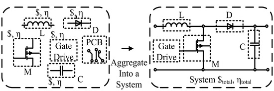
1.2. Proposed Approach and Contribution
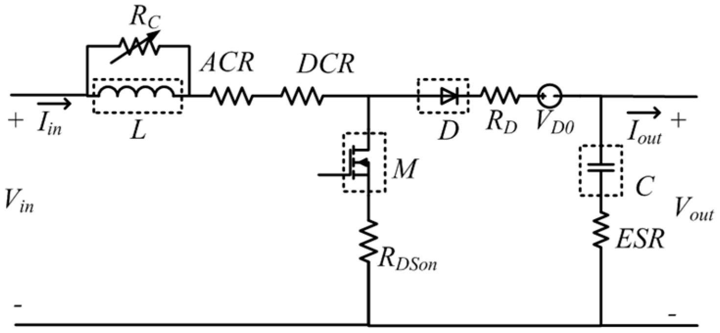
2. Generalized Component-Level Power Loss Models
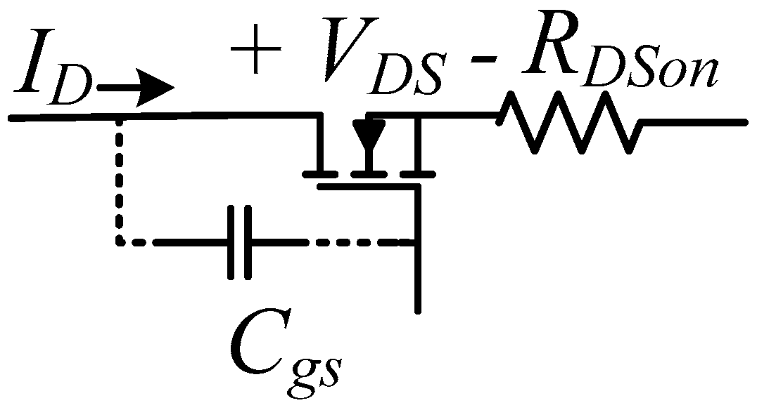
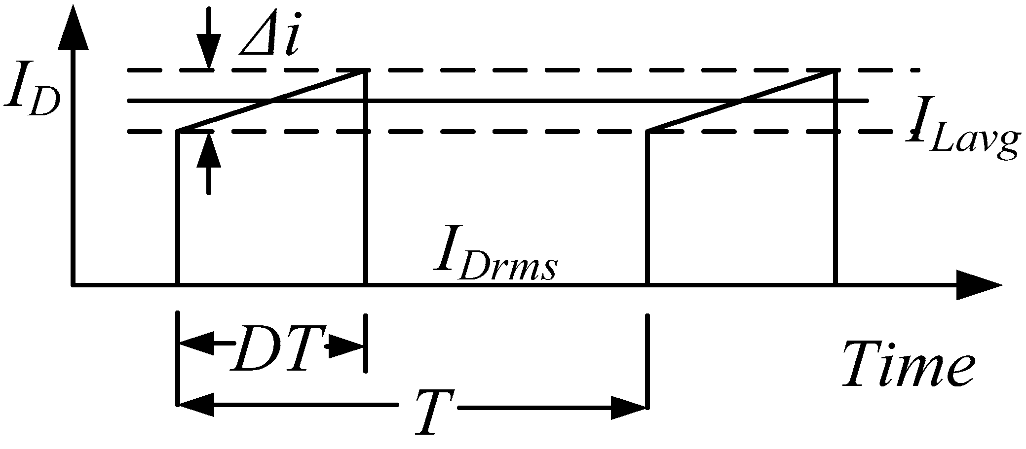
2.1. MOSFET Losses
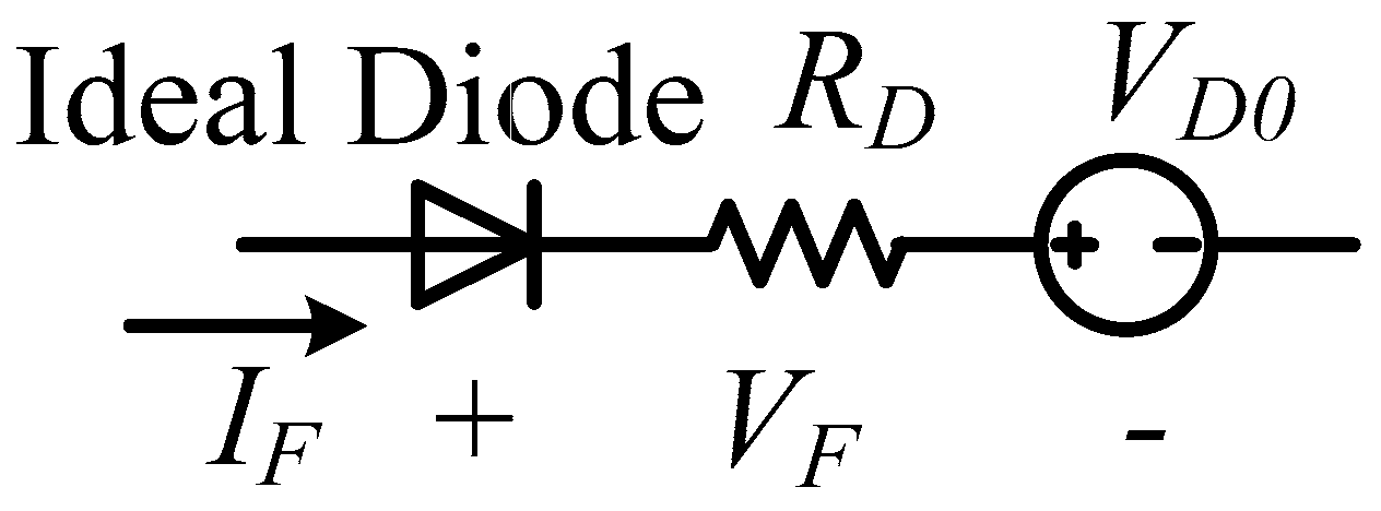
2.2. Diode Losses
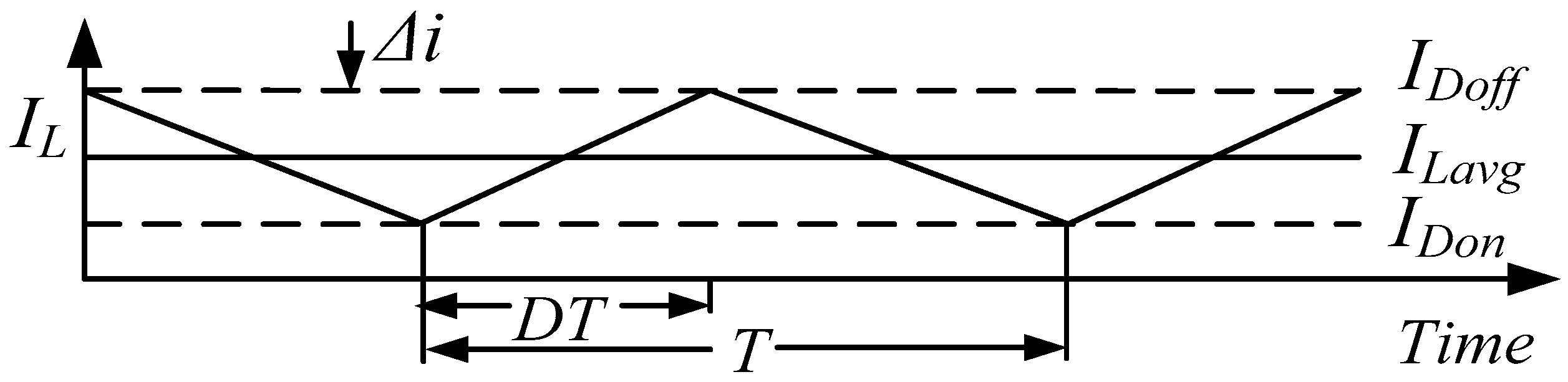
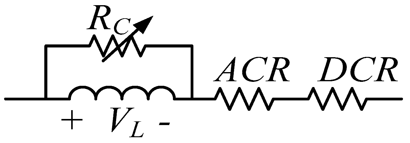
2.3. Inductor Losses
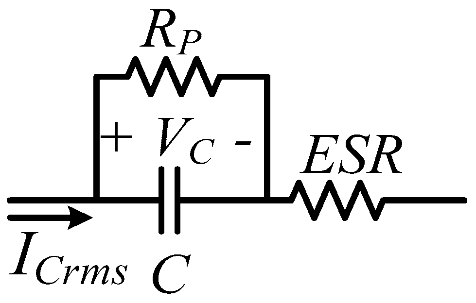
2.4. Capacitor Losses
3. Power Loss Models for Several Converters
3.1. Boost Converter in CCM
3.1.1. MOSFET Losses
3.1.2. Diode Losses
3.1.3. Inductor Losses
3.1.4. Capacitor Losses
3.2. Buck Converter in CCM
3.2.1. MOSFETs Losses
3.2.2. Diode Losses
3.2.3. Inductor Losses
3.2.4. Capacitor Losses
3.3. Flyback Converter in DCM
3.3.1. MOSFET Losses
3.3.2. Diode Losses
3.3.3. Flyback Coupled-Inductor/Transformer Lossses
3.3.4. Capacitor Losses
3.3.5. Snubber Circuit Losses
4. Major Component Cost Models
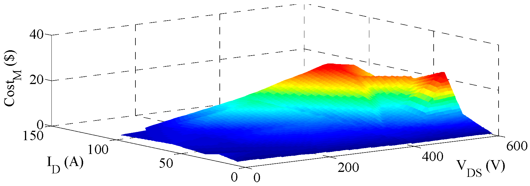
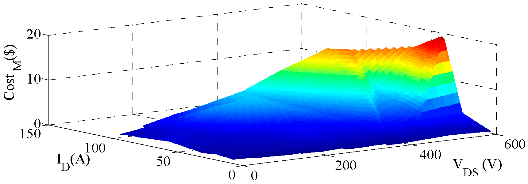
4.1. MOSFETs
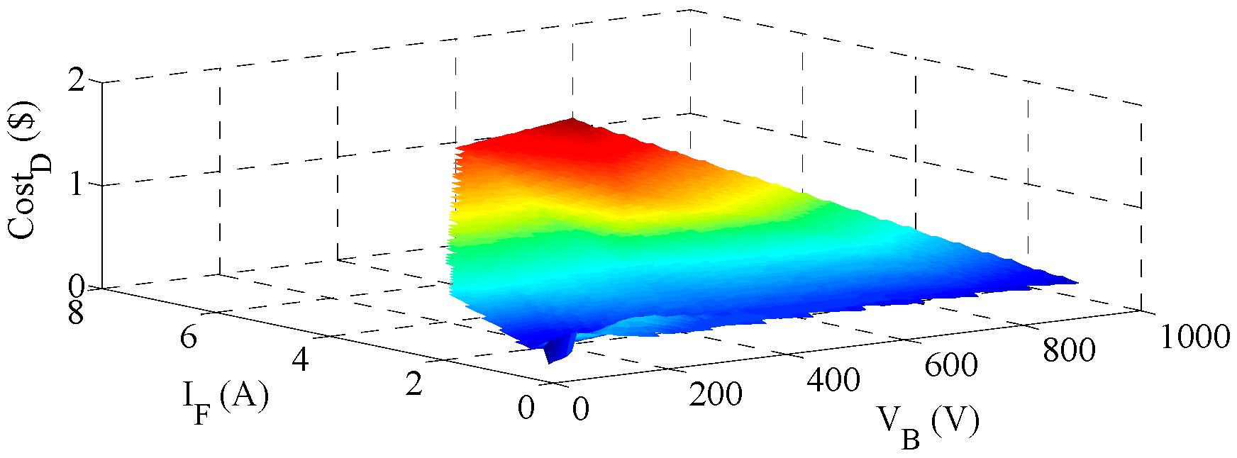
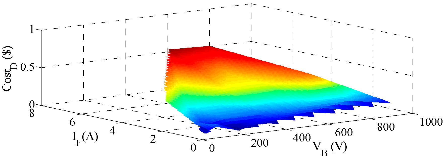
4.2. Diodes
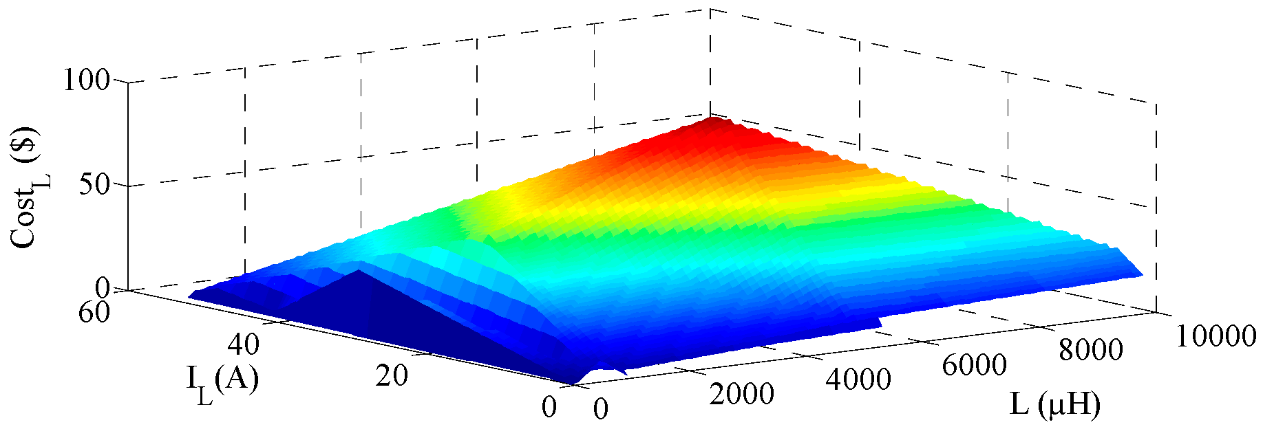
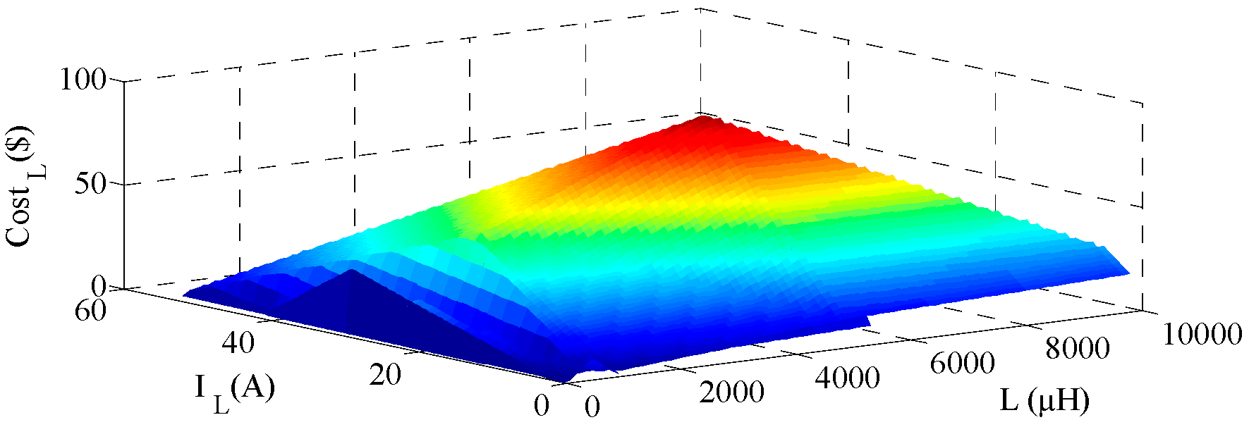
4.3. Inductors
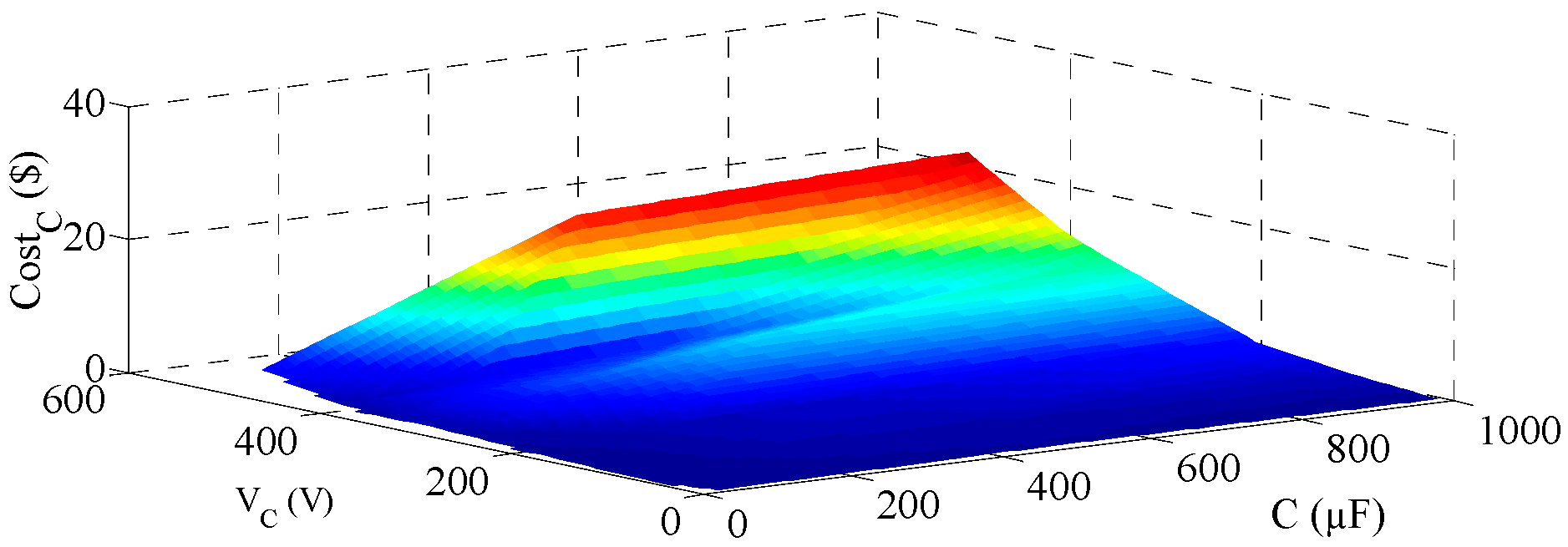
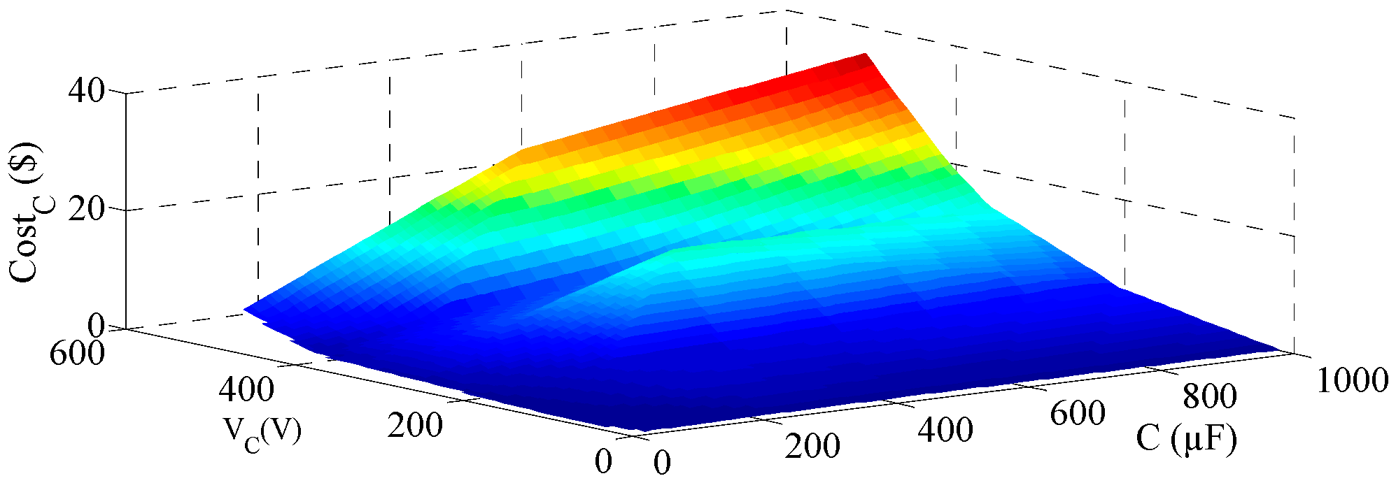
4.4. Capacitors
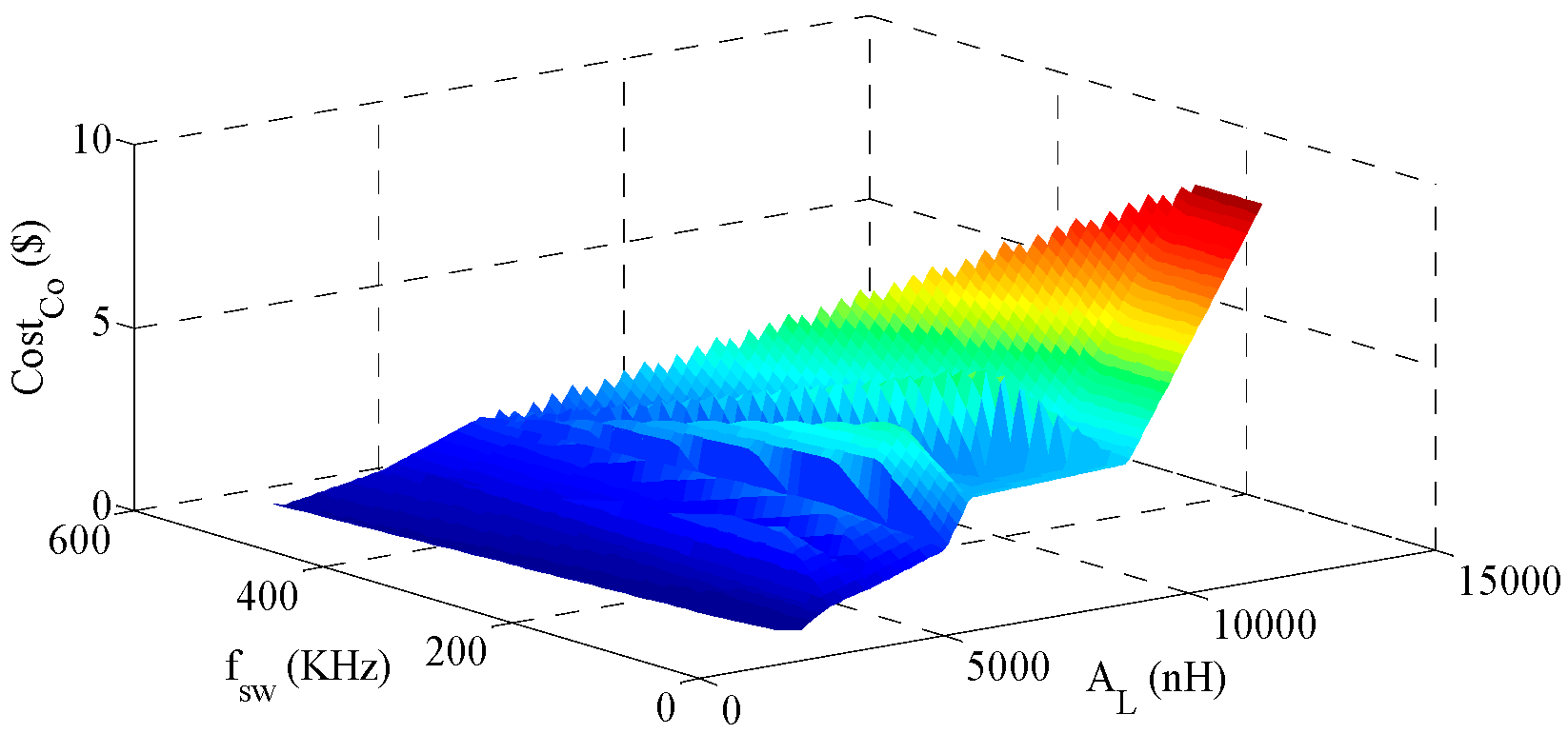
4.5. Flyback Coupled-Inductor Core
5. Results
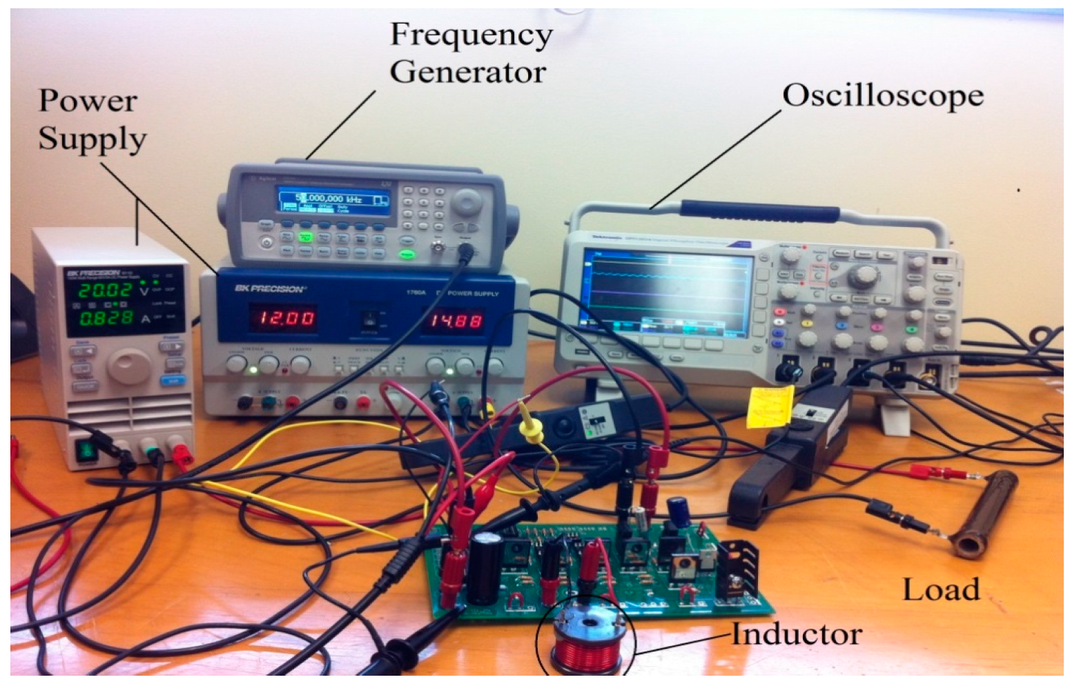
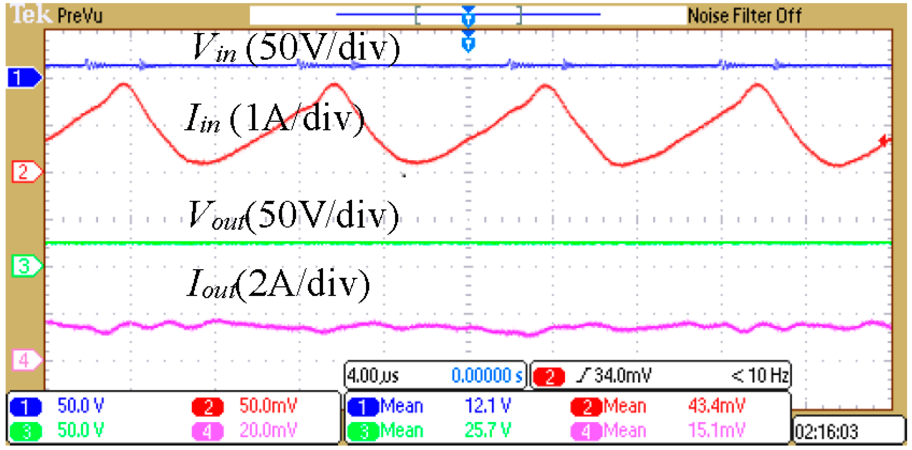
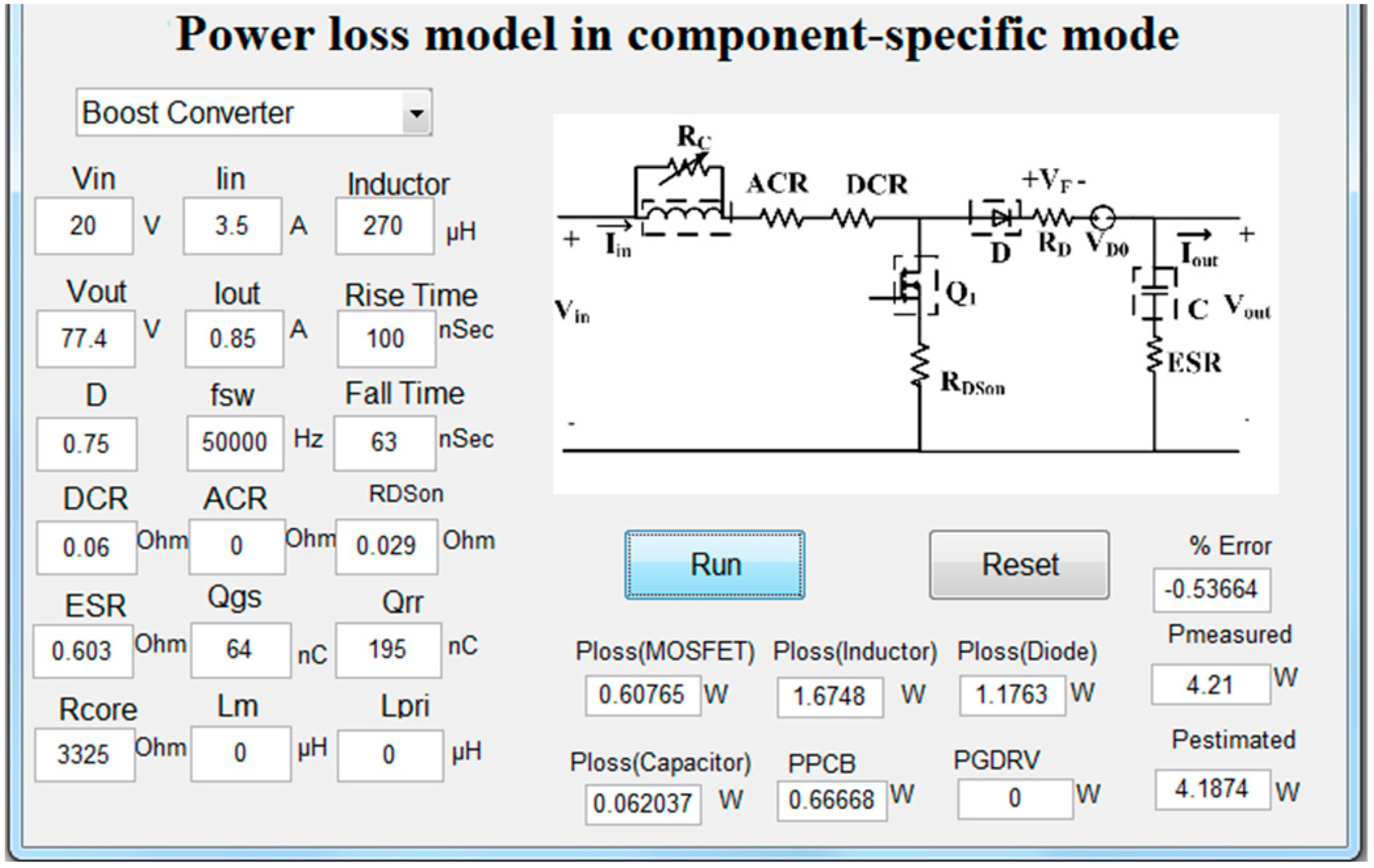
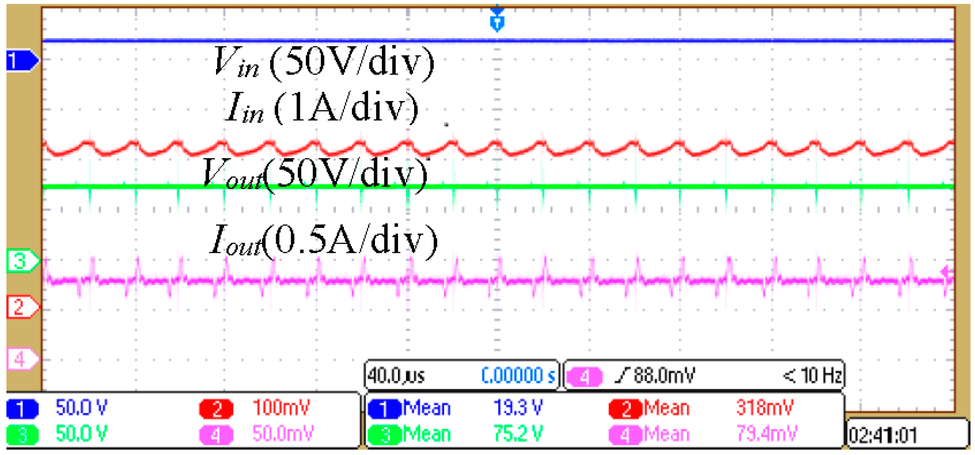
5.1. Power Loss Model Verification
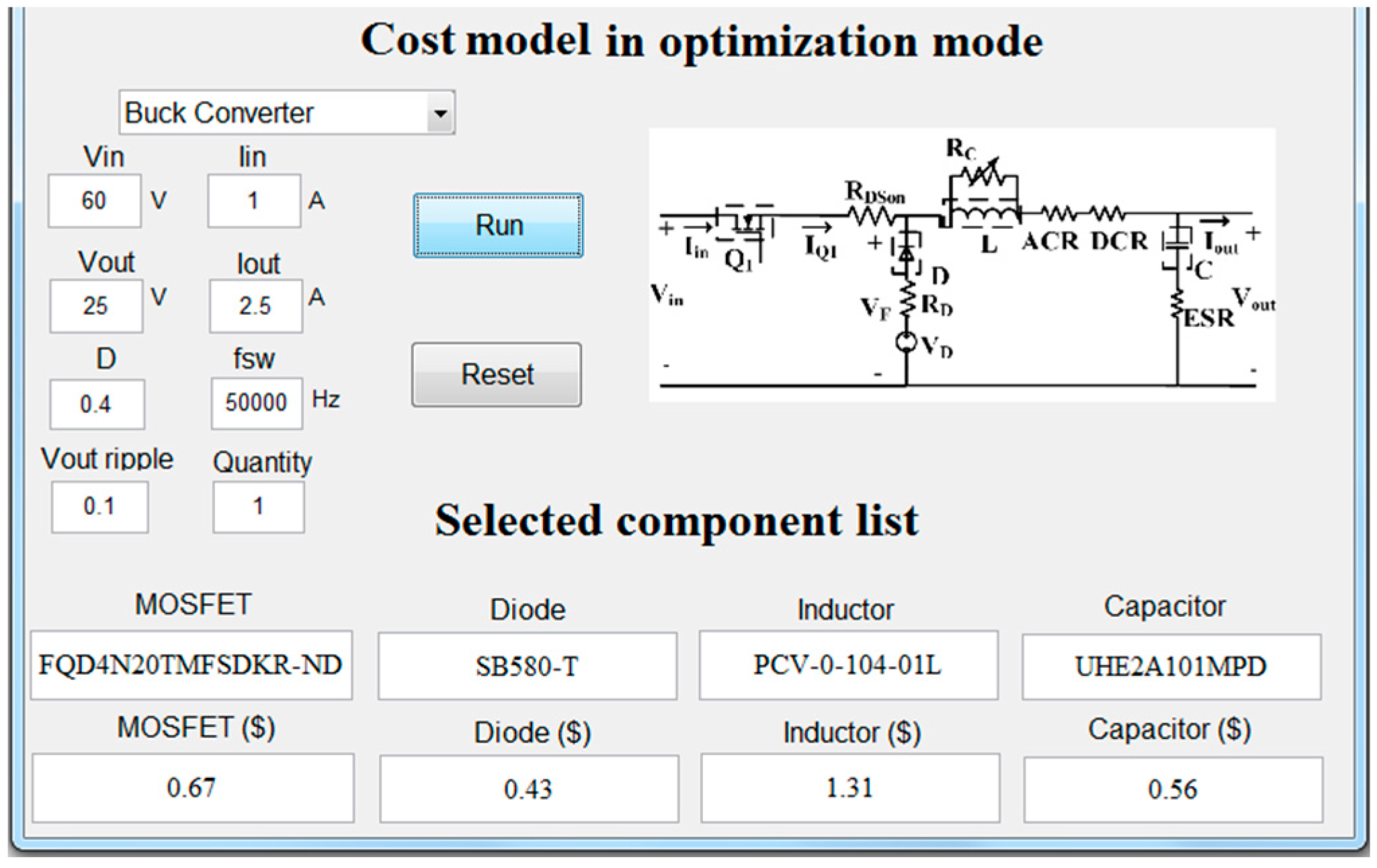
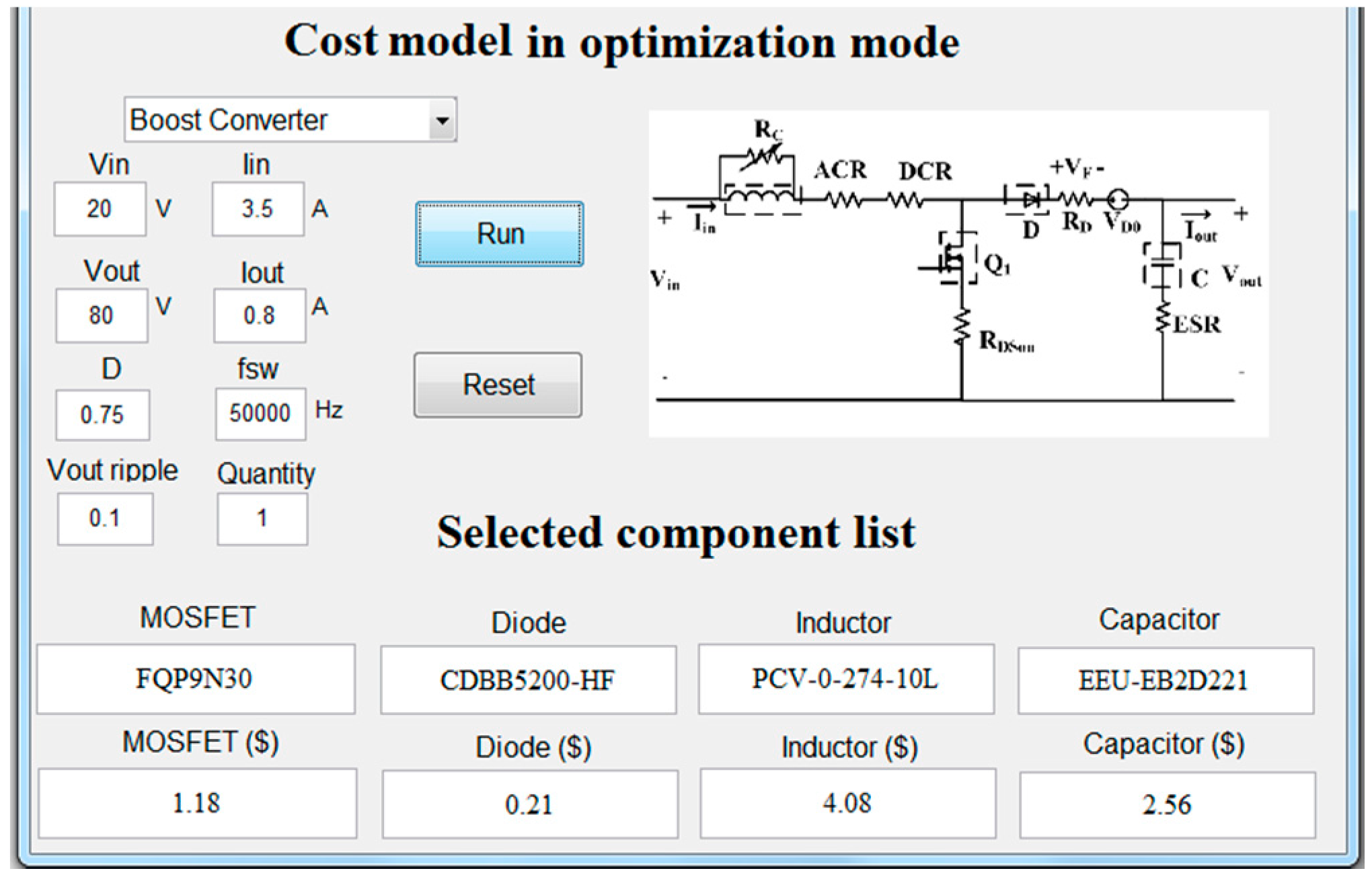
5.2. Cost Model Verification
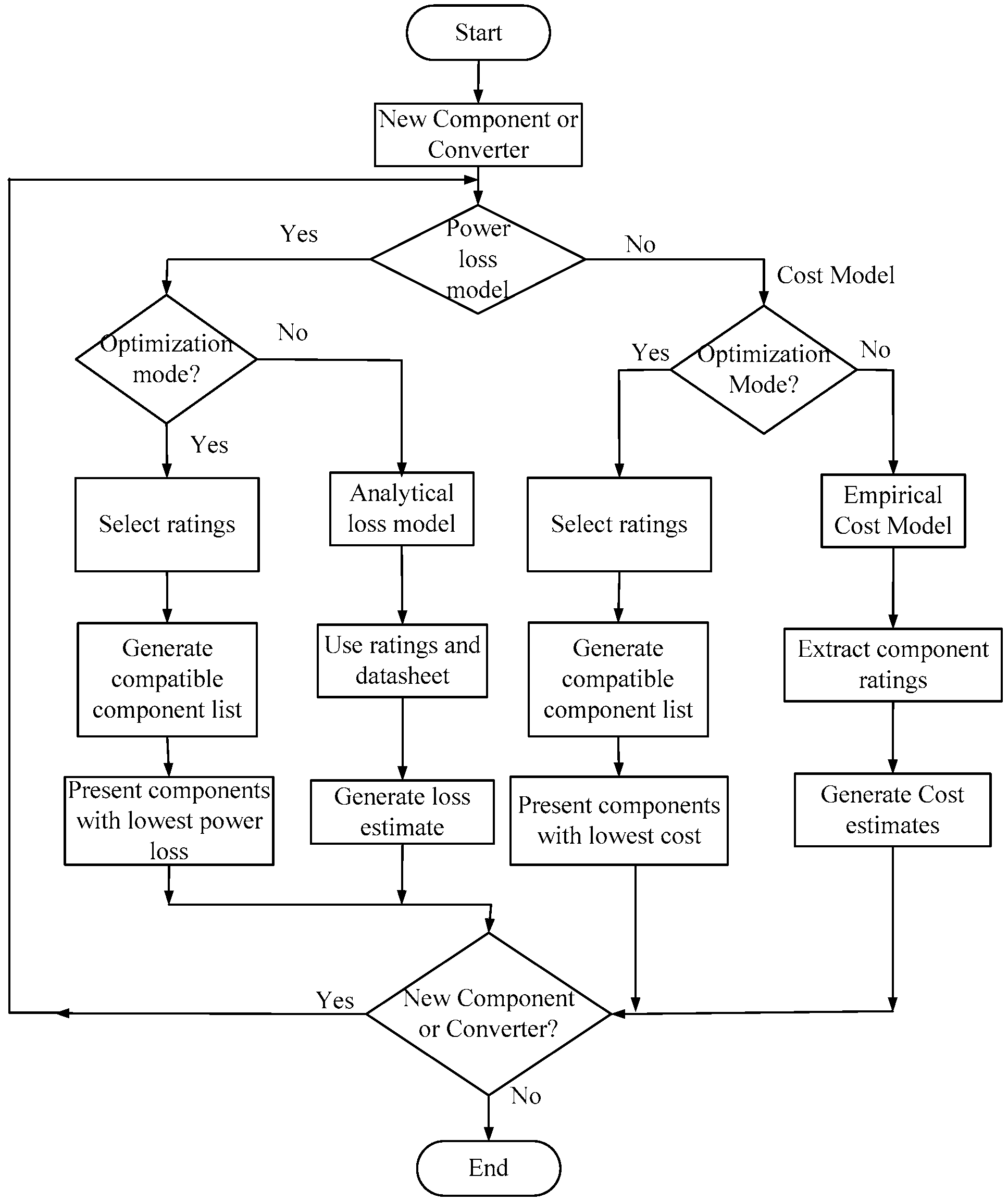
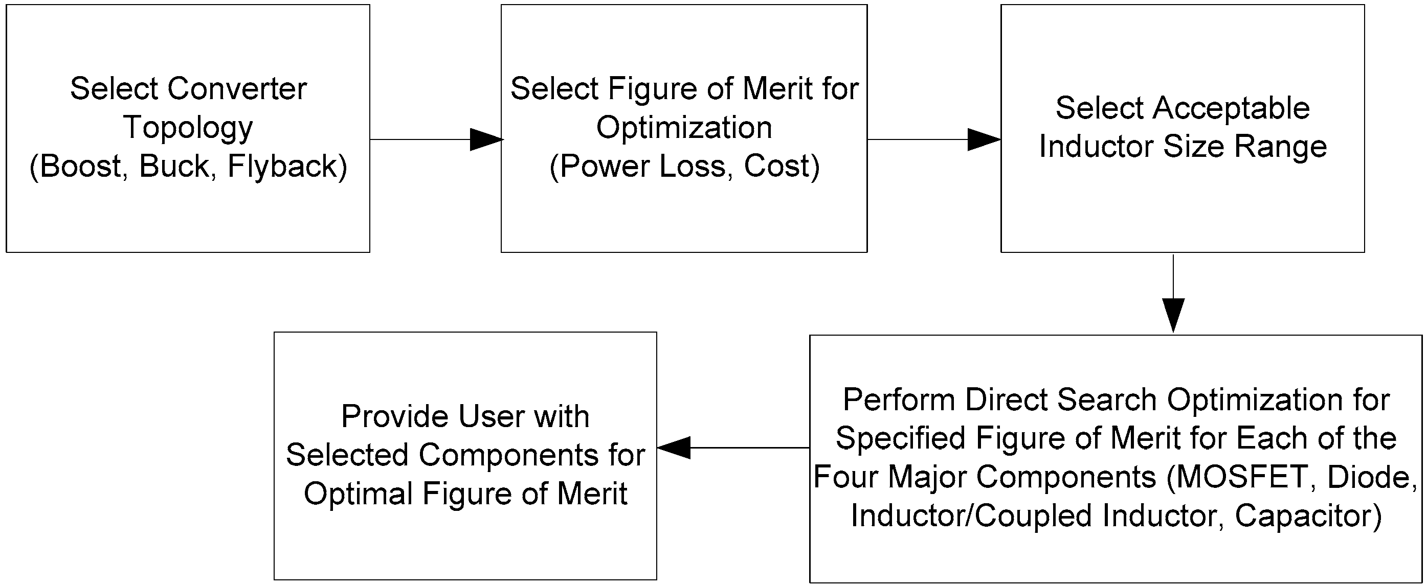
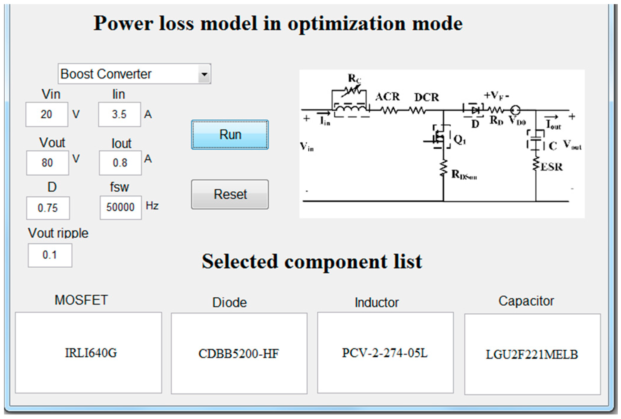
6. Optimization of Converter Designs for a Specific Figure of Merit
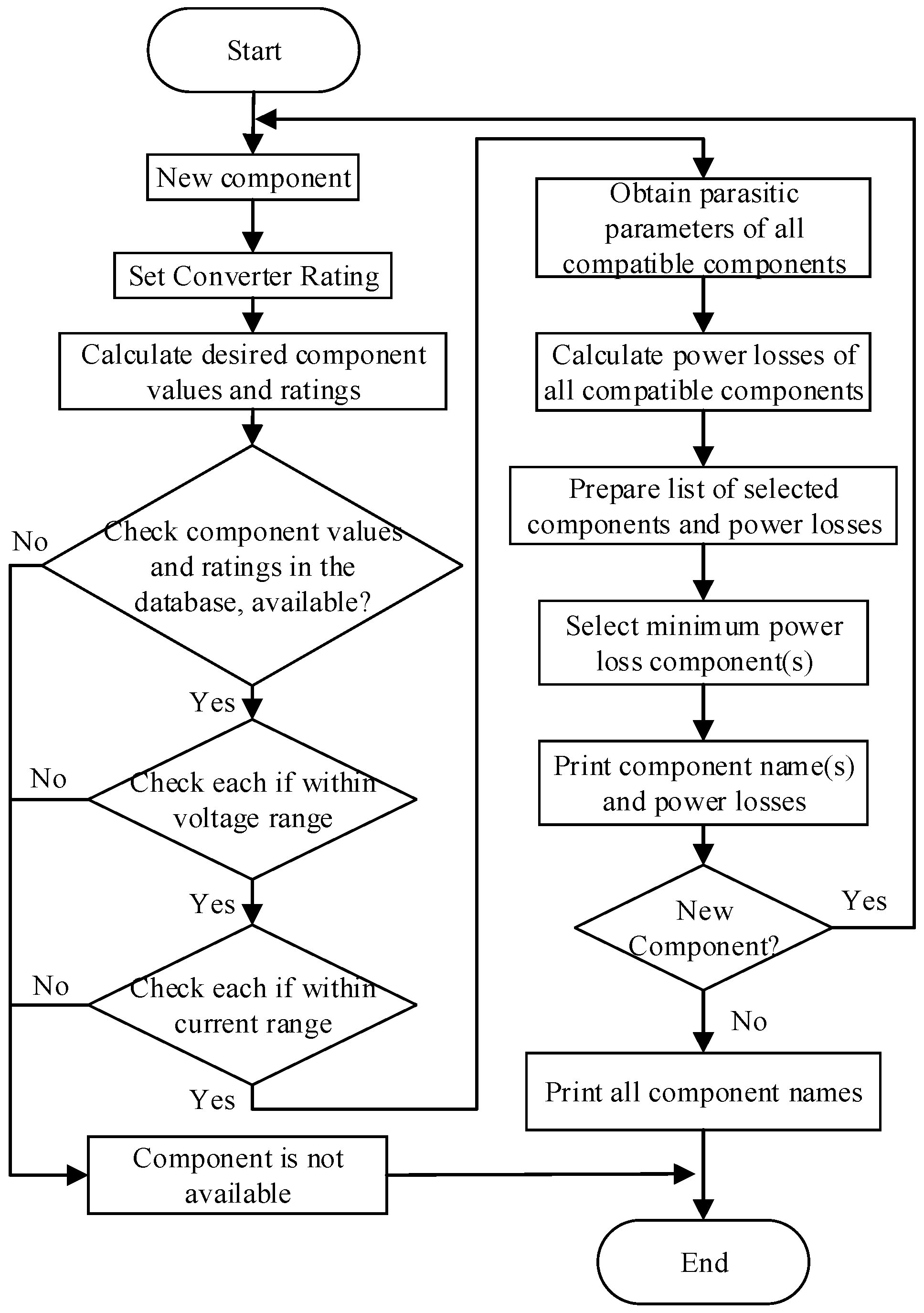
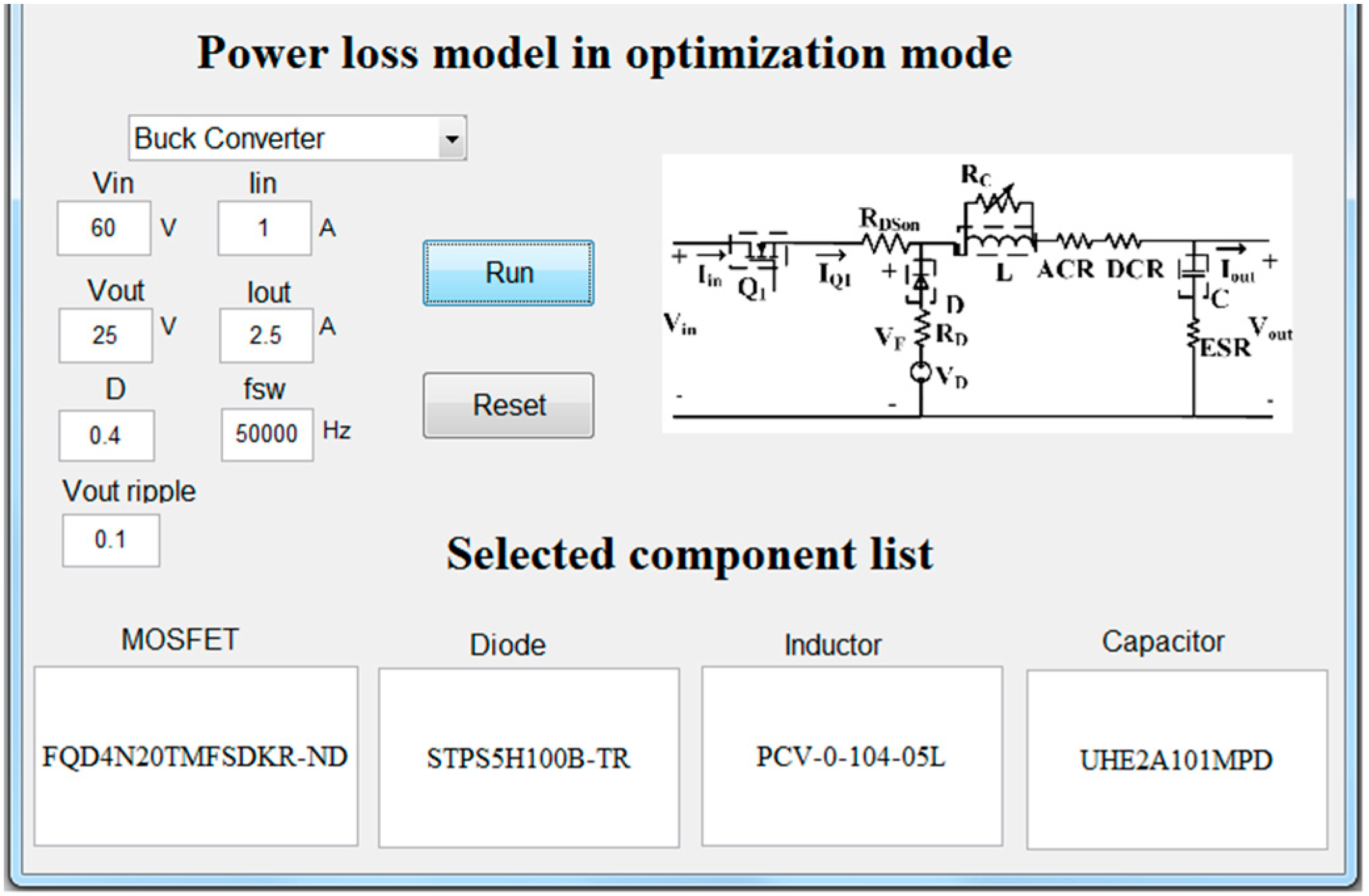
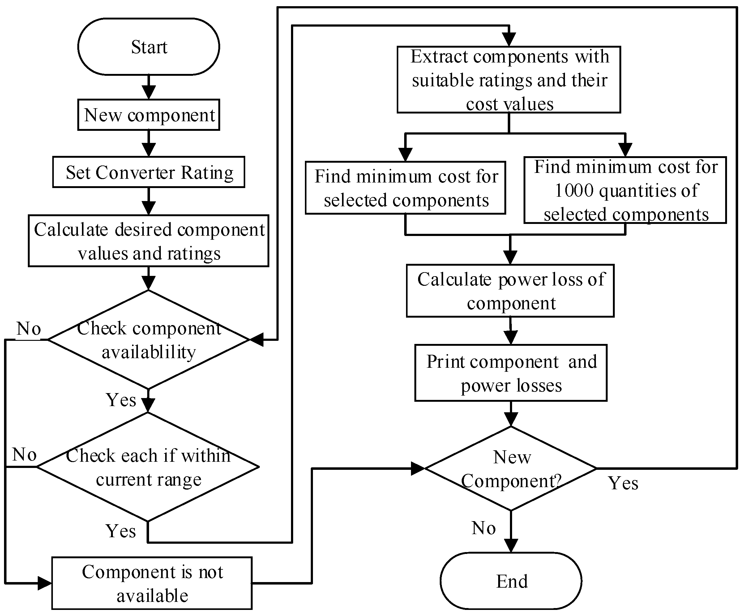
6.1. Optimal Design Selection Approach
6.2. Minimum Power Loss Designs
| Start |
| Get input and output parameters; |
| IL = Iin; |
| L = ((Vin × D × (1 − D))/(2 × fsw × Iout)); |
| Lmax = 2 × L; |
| Read inductor.xls file and get the entire database; |
| for i = 1 to all database |
| if L <= inductor values in database && |
| Lmax > inductor values in database |
| if IL <= inductor current values in database |
| Extract ACR, DCR and RC values from the database; |
| end if; |
| end if; |
| i = i + 1; |
| end if; |
| Calculate PACR, PDCR and PCORE as described in power loss model |
| Ploss_inductor = PACR + PDCR + PCORE; |
| Print component name; |
6.3. Minimum Cost Designs
| Start |
| Get input and output parameters; |
| L = ((Vin × D × (1-D))/(2 × fsw × Iout)); Lmax = 2 × L; |
| Read inductor.xls file and get all the database; |
| for i = 1 to all database |
| if L <= inductor values in database && Lmax > inductor values in database |
| Extract ACR, DCR and RC values from database; |
| Extract unit costs and multiple unit costs data base; |
| end i = i + 1; |
| end |
| Find minimum cost of the component |
| Print minimum cost of the component for unit quantity; |
| Calculate PACR, PDCR and PCORE as described in power loss model; |
| Ploss_inductor = PACR + PDCR + PCORE; |
| Print component name; Print component cost; |
7. Conclusions
Author Contributions
Conflicts of Interest
Abbreviations
| A | Plate area in mm2 |
| AC | Core cross-sectional area |
| AL | Inductance factor |
| ACR | Inductor ac resistance |
| B | The peak flux density |
| BβAC | AC component of flux density |
| ∆Bm, ∆Bmax | Maximum peak flux density |
| C | Capacitance value |
| Cgs | MOSFET gate-to-source capacitance |
| CostC | Capacitor cost model |
| CostCO | Core cost model |
| CostD | Diode cost model |
| CostL | Inductor cost model |
| CostM | MOSFET cost model |
| CostW | Wire cost model |
| Csn | Snubber capacitor |
| Cstray | PCB stray capacitance |
| d | Plate separation in mm |
| D | Duty ratio |
| DCR | Inductor DC resistance |
| Dsn | Snubber diode |
| Er | Dielectric constant for air |
| ESR | Equivalent series resistance |
| f | Inductor Current frequency |
| fsw | Switching frequency |
| G | Wire gauge |
| H | Height of PCB trace |
| Δi | Inductor ripple current |
| ICrms | Capacitor RMS current |
| IDrms, ID | Drain-to-source RMS current |
| IDon, IDoff | MOSFET on- and off-current |
| ∆IF | Change in diode forward current |
| IFavg, IFrms | Diode avg. and RMS fwd. current |
| IDsn(avg) | Snubber diode average current |
| IDsn(rms) | Snubber diode RMS current |
| Iin | Converter input current |
| IL | Inductor current |
| ILavg, ILrms | Inductor avgerage and RMS current |
| Iout | Converter output current |
| IQBS, IQCC | Gate drive quiescent currents |
| ISrms | Snubber branch RMS current |
| Itrace | PCB trace current |
| K1 | Inductor core material constant |
| Kfe | Inductor current material constant at fsw |
| L | Inductance value in |
| Le | Length of PCB trace |
| Lm | Mutual inductance |
| Lpri | Primary inductance |
| Lsec | Secondary inductance |
| Lstray | PCB stray inductance |
| n | Transformation ratio |
| Npri | Primary windings number of turns |
| Nsec | Secondary windings number of turns |
| Pac | Capacitor AC loss |
| PACR | Inductor AC resistance loss |
| PBT | Power dissipated at the bootstrap pin |
| PCD | Diode conduction loss |
| PCDsn | Snubber diode power loss |
| Pclamp | Power loss in the clamp unit |
| PCM | MOSFET conduction loss |
| PCORE | Inductor or flyback transformer core loss |
| PCstray | PCB stray capacitance loss |
| Pdc | Capacitor DC loss |
| PDCR | Inductor DC resistance loss |
| PG | MOSFET gate loss |
| PGDRV | Gate drive power loss |
| Ploss(Capacitor) | Total capacitor power loss |
| Ploss(Diode) | Total diode power loss |
| Ploss(Inductor) | Total inductor power loss |
| Ploss(MOSFET) | Total MOSFET power loss |
| PON(M) | MOSFET turn-on loss |
| POFF(M) | MOSFET turn-off loss |
| PPCB | Total PCB power loss |
| PRpri | Flyback transformer primary power loss |
| PRsec | Flyback transformer secondary power loss |
| Pstray | PCB stray inductance power loss |
| PSW | MOSFET total switching losses |
| PSWD | Diode switching loss |
| PSWDsn | Snubber diode switching loss |
| PTotal | Total converter power loss |
| Ptrace | PCB trace power loss |
| PVCC | Power drawn through the gate drive supply pin |
| Qg | Bootstrap capacitor charge |
| Qgs | Gate-to-source charge |
| Qrr | Diode reverse recovery charge |
| RC | Effective core impedance |
| RDsn | Snubber diode on-resistance |
| RD | Diode on-resistance |
| RDSon | Drain-to-source resistance |
| RLoad | Output load resistor |
| Rsn | Snubber resistor |
| Rp | Capacitor parallel resistor |
| Rpri | Primary DC resistance |
| Rsec | Secondary DC resistance |
| Rtrace | PCB trace resistance |
| tr, tf | MOSFET rise and fall times |
| VB | Diode DC blocking voltage |
| VBT | Gate drive IC Bootstrap voltage |
| VC | Capacitor voltage |
| Vclamp | Clamp voltage rise |
| VCC | Gate drive IC Supply voltage |
| Vd | Voltage difference between dielectric material |
| VD0, VDsn0 | Diode initial state voltage |
| VDmax, VDtyp | Diode maximum and typical fwd. voltage |
| VDS, Vds | Drain to source voltage |
| VDSBR | Drain to source breakdown voltage |
| Ve | Effective core volume |
| ∆VF | Change in diode fwd. voltage |
| Vin | Converter input voltage |
| VL | Inductor voltage |
| Vout | Converter output voltage |
| ∆Vout | Converter output voltage ripple |
| Vrr | Reverse recovery voltage |
| Vsupply | Supply voltage |
| W | Width of PCB trace |
| x, y | Core loss coefficients |
Appendix A

| Parameters | Boost Converter | Buck Converter | ||||
|---|---|---|---|---|---|---|
| Case 1 | Case 2 | Case 3 | Case 1 | Case 2 | Case 3 | |
| Vin (V) | 50 | 40 | 20 | 50 | 200 | 200 |
| Iin (A) | 4 | 2.1 | 2 | 0.5 | 2 | 1.5 |
| Vout (V) | 120 | 80 | 130 | 25 | 160 | 120 |
| Iout (A) | 2.1 | 0.9 | 0.3 | 1 | 2.5 | 2.5 |
| Duty | 0.6 | 0.5 | 0.85 | 0.5 | 0.8 | 0.6 |
| fsw (KHz) | 100 | 100 | 50 | 50 | 50 | 100 |
| Voutripple (V) | 0.1 | 0.1 | 0.1 | 0.2 | 0.1 | 0.2 |
| MOSFET | Diode | ||
|---|---|---|---|
| Suitable Components | PLoss (W) | Suitable Components | PLoss (W) |
| FQP9N30 | 6.05 | RD0504T-TL-H | 3.63 |
| STP12NK30Z | 4.19 | BY229B-400HE3/45 | 5.53 |
| IRF740PBF | 5.87 | STTH5L04DEE-TR | 3.26 |
| IRF740STRLPBF | 5.87 | Capacitor | |
| SiHB10N40D | 6.14 | Suitable Components | PLoss (W) |
| Inductor | LGU2F221MELB | 0.00022 | |
| Suitable Components | PLoss (W) | ECO-S2GB221EA | 0.027 |
| PCV-2-274-03L | 4.42 | ||
| PCV-2-274-05L | 1.60 | ||
| PCV-2-274-10L | 2.05 | ||
| MOSFET | Inductor | ||
|---|---|---|---|
| Suitable Components | PLoss (W) | Suitable Components | PLoss (W) |
| FQD7N20LTMDKR | 2.47 | PCV-2-394-05L | 1.32 |
| BUZ73AL H-ND | 1.86 | ||
| JAN2N6798U-MIL | 1.28 | ||
| FQD7N30TMTR-ND | 2.027 | Capacitor | |
| Diode | Suitable Components | PLoss (W) | |
| Suitable Components | PLoss (W) | EEU-ED2C470 | 0.00022 |
| S320 | 1.77 | UPB2E470MHD1TO | 0.00022 |
| PDS3200-13 | 1.66 | ECO-S2GA470BA | 0.022 |
| GI912-E3/73 | 2.01 | 380LX470M500H012 | 0.0055 |
| MOSFET | Diode | ||
|---|---|---|---|
| Suitable Components | PLoss (W) | Suitable Components | PLoss (W) |
| FQD7N30TMTR-ND | 2.51 | UVZ2F101MHD | 0.00019 |
| IRF730PBF | 3.46 | UPT2G101MHD6 | 0.00019 |
| IRF730STRRPBF | 3.46 | Inductor | |
| STP7NK40Z | 3.45 | Suitable Components | PLoss (W) |
| STD9NM40N | 2.72 | PCV-2-564-02L | 12.71 |
| STD6NK50ZT4 | 4.16 | PCV-2-564-06L | 8.05 |
| FDD6N50FTM | 4.00 | PCV-2-564-08L | 4.25 |
| NDF05N50ZH | 5.17 | DO5040H-684KLB | 37.93 |
| Diode | |||
| Suitable Components | PLoss (W) | ||
| RGP30G-E3/73 | 0.64 | ||
| MOSFET | Inductor | ||
|---|---|---|---|
| Suitable Components | PLoss (W) | Suitable Components | PLoss (W) |
| FQT7N10LTFCT-ND | 0.43 | PCV-2-223-05L | 0.05 |
| FQT7N10LTFDKR-ND | 0.43 | PCV-2-223-10L | 0.049 |
| FQT7N10TFTR-ND | 0.30 | RFB1010-221L | 3.48 |
| ZXMN20B28KTCCTN | 0.66 | CV-0-224-03L | 0.14 |
| ZXMN20B28KTCDKR | 0.66 | ||
| Diode | |||
| Suitable Components | PLoss (W) | ||
| SS15 | 0.95 | Capacitor | |
| GF1A-E3/67A | 1.096 | Suitable Components | PLoss (W) |
| SS15E-TP | 0.89 | EEU-FC2A220 | 0.074 |
| SK15-13-F | 0.91 | EKXG401ELL220 | 0.25 |
| SS18-TP | 0.84 | EEU-EB2D220 | 0.16 |
| SS18 | 0.95 | UPJ2F220MHD1TN | 0.21 |
| B180-13-F | 0.92 | ||
| CDBA180-G | 0.96 | ||
| RS1B-E3/5AT | 1.17 | ||
| CDBM1100-G | 0.96 | ||
| SS110-TP | 0.84 | ||
| SB1100 | 0.96 | ||
| MOSFET | Diode | ||
|---|---|---|---|
| Suitable Components | PLoss (W) | Suitable Components | PLoss (W) |
| IRF730PBF | 7.084 | RGP30G-E3/73 | 1.16 |
| IRF730STRRPBF | 7.084 | RD0504T-TL-H | 1.037 |
| STP7NK40Z | 7.038 | STTH5L04DEE-TR | 0.87 |
| STD9NM40N | 5.47 | BYC5DX-500,127 | 1.062 |
| STD6NK50ZT4 | 8.63 | RGP30J-E3/73 | 1.075 |
| FDD6N50FTM | 8.41 | CN649 | 0.98 |
| NDF05N50ZH | 10.47 | LXA03B600 | 1.75 |
| STP8N80K5 | 6.94 | BYV25D-600,118 | 0.98 |
| SPD06N80C3 | 6.73 | LQA05TC600 | 1.28 |
| IXTH6N80A | 10.77 | Capacitor | |
| Inductor | Suitable Components | PLoss (W) | |
| Suitable Components | PLoss (W) | UPT2G101MHD6 | 0.013 |
| PCV-2-223-05L | 0.19 | ||
| PCV-2-223-10L | 0.17 | ||
| PCH-27X-223_LT | 136.30 | ||
| PCV-0-224-03L | 1.048 | ||
| MOSFET | Diode | ||
|---|---|---|---|
| Suitable Components | PLoss (W) | Suitable Components | PLoss (W) |
| IRF720 | 9.74 | RGP30G-E3/73 | 2.27 |
| IRF720SPBF | 9.74 | RD0504T-TL-H | 2.018 |
| IRF720STRRPBF | 9.74 | STTH5L04DEE-TR | 1.74 |
| IRF730PBF | 5.83 | Inductor | |
| IRF730STRRPBF | 5.83 | Suitable Components | PLoss (W) |
| STP7NK40Z | 5.74 | PCV-0-104-01L | 4.63 |
| STD9NM40N | 4.36 | PCV-0-104-03L | 1.75 |
| STD6NK50ZT4 | 7.26 | PCV-0-104-05L | 1.34 |
| FDD6N50FTM | 7.24 | Capacitor | |
| NDF05N50ZH | 8.43 | Suitable Components | PLoss (W) |
| STP8N80K5 | 5.95 | UPB2E470MHD1TO | 0.021 |
| SPD06N80C3 | 5.96 | ECO-S2GA470BA | 2.058 |
| IXTH6N80A | 9.883333333 | 380LX470M500H012 | 0.520833 |
| 380LX470M500H012 | |||
| MOSFET | Diode | ||
|---|---|---|---|
| Suitable Components | Cost ($) | Suitable Components | Cost ($) |
| FQP9N30 | 1.18 | RD0504T-TL-H | 1.05 |
| STP12NK30Z | 1.95 | BY229B-400HE3/45 | 1.03 |
| IRF740PBF | 1.63 | BYC5DX-500,127 | 0.35 |
| IRF740STRLPBF | 1.63 | BYV25D-600,118 | 0.848 |
| SiHB10N40D | 1.79 | LQA05TC600 | 1.41 |
| Inductor | MURF860G | 0.99 | |
| Suitable Components | Cost ($) | LQA08TC600 | 1.93 |
| PCV-2-274-03L | 4.15 | QH08TZ600 | 1.85 |
| PCV-2-274-05L | 4.56 | Capacitor | |
| P CV-2-274-10L | 7.39 | Suitable Components | Cost ($) |
| LGU2F221MELB | 7.022 | ||
| ECO-S2GB221EA | 4.68 | ||
| MOSFET | Diode | ||
|---|---|---|---|
| Suitable Components | Cost ($) | Suitable Components | Cost ($) |
| FQD7N20LTMDKR-ND | 0.98 | GI912-E3/73 | 0.48 |
| BUZ73AL H-ND | 1.26 | RGP30G-E3/73 | 0.45 |
| JAN2N6798U-MIL | 4.34 | RD0504T-TL-H | 1.05 |
| RDN100N20FU6-ND | 2.73 | Capacitor | |
| RDN100N20-ND | 2.73 | Suitable Components | Cost ($) |
| IRLI640GPBF | 2.88 | EEU-ED2C470 | 0.72 |
| IRLI640G | 2.88 | UPB2E470MHD1TO | 1.67 |
| FQD7N30TMTR-ND | 1.04 | ECO-S2GA470BA | 1.31 |
| FQP9N30 | 1.18 | 380LX470M500H012 | 5.41 |
| STP12NK30Z | 1.95 | Inductor | |
| Suitable Components | Cost ($) | ||
| PCV-2-394-05L | 5.1 | ||
| MOSFET | Inductor | ||
|---|---|---|---|
| Suitable Components | Cost ($) | Suitable Components | Cost ($) |
| FQD7N30TMTR-ND | 1.04 | PCV-2-564-02L | 3.78 |
| FQP9N30 | 1.18 | PCV-2-564-06L | 6.46 |
| STP12NK30Z | 1.95 | PCV-2-564-08L | 10.79 |
| IRF730PBF | 1.26 | Capacitor | |
| IRF730STRRPBF | 1.51 | Suitable Components | Cost ($) |
| STP7NK40Z | 1.56 | UVZ2F101MHD | 1.85 |
| STD9NM40N | 1.67 | UPT2G101MHD6 | 2.68 |
| IRF740PBF | 1.63 | ||
| IRF740STRLPBF | 1.63 | Diode | |
| SiHB10N40D | 1.79 | Suitable Components | Cost ($) |
| STD6NK50ZT4 | 1.18 | LQA05TC600 | 1.41 |
| FDD6N50FTM | 1.1 | RGP30G-E3/73 | 0.45 |
| NDF05N50ZH | 0.94 | RD0504T-TL-H | 1.05 |
| TK10A50D | 1.89 | BYC5DX-500,127 | 0.35 |
| STP11NK50ZFP | 1.93 | RGP30J-E3/73 | 0.495 |
| IPA50R350CP | 1.12 | LXA03B600 | 0.81 |
| FDPF12N50UT | 1.73 | BYV25D-600,118 | 0.848 |
| MOSFET | Inductor | ||
|---|---|---|---|
| Suitable Components | Cost ($) | Suitable Components | Cost ($) |
| FQT7N10LTFCT-ND | 0.54 | PCV-2-223-05L | 2.12 |
| FQT7N10LTFDKR-ND | 0.54 | PCV-2-223-10L | 2.06 |
| FQT7N10TFTR-ND | 0.54 | PCH-27X-223_LT | 1.91 |
| Diode | RFB1010-221L | 0.68 | |
| Suitable Components | Cost ($) | PCV-0-224-03L | 1.46 |
| SS18-TP | 0.39 | Capacitor | |
| SS18 | 0.46 | Suitable Components | Cost ($) |
| B180-13-F | 0.82 | EEU-FC2A220 | 0.502 |
| CDBA180-G | 0.54 | EKXG401ELL220 | 1.72 |
| RS1B-E3/5AT | 0.178 | EEU-EB2D220 | 0.69 |
| CDBM1100-G | 0.57 | UPJ2F220MHD1TN | 1.324 |
| SS110-TP | 0.39 | ||
| SB1100 | 0.52 | ||
| MOSFET | Diode | ||
|---|---|---|---|
| Suitable Components | Cost ($) | Suitable Components | Cost ($) |
| IRF730PBF | 1.26 | RGP30G-E3/73 | 0.45 |
| IRF730STRRPBF | 1.51 | RD0504T-TL-H | 1.05 |
| STP7NK40Z | 1.56 | STTH5L04DEE-TR | 1.49 |
| STD9NM40N | 1.67 | BYC5DX-500,127 | 0.35 |
| STD6NK50ZT4 | 1.18 | RGP30J-E3/73 | 0.49 |
| FDD6N50FTM | 1.1 | CN649 | 0.45 |
| NDF05N50ZH | 0.94 | LXA03B600 | 0.81 |
| Inductor | BYV25D-600,118 | 0.84 | |
| Suitable Components | Cost ($) | LQA05TC600 | 1.41 |
| PCV-2-223-05L | 2.12 | ||
| PCV-2-223-10L | 2.06 | Capacitor | |
| PCH-27X-223_LT | 1.91 | Suitable Components | Cost ($) |
| PCV-0-224-03L | 1.46 | UPT2G101MHD6 | 2.68 |
| MOSFET | Diode | ||
|---|---|---|---|
| Suitable Components | Cost ($) | Suitable Components | Cost ($) |
| IRF720 | 3.18 | RGP30G-E3/73 | 0.45 |
| IRF720SPBF | 1.51 | RD0504T-TL-H | 1.05 |
| IRF720STRRPBF | 1.51 | STTH5L04DEE-TR | 1.49 |
| IRF730PBF | 1.26 | Inductor | |
| IRF730STRRPBF | 1.51 | Suitable Components | Cost ($) |
| STP7NK40Z | 1.56 | PCV-0-104-01L | 1.31 |
| STD9NM40N | 1.67 | PCV-0-104-03L | 1.48 |
| STD6NK50ZT4 | 1.18 | PCV-0-104-05L | 2.37 |
| FDD6N50FTM | 1.1 | Capacitor | |
| NDF05N50ZH | 0.94 | Suitable Components | Cost ($) |
| UPB2E470MHD1TO | 1.67 | ||
| ECO-S2GA470BA | 1.31 | ||
| 380LX470M500H012 | 5.41 | ||
| 380LX470M500H012 | |||
Appendix B
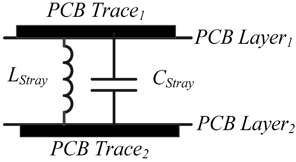
Appendix B.1. PCB Losses

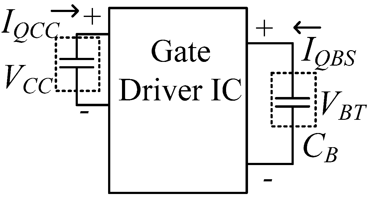
Appendix B.2. Gate Drive Losses
References
- Ma, K.; Blaabjerg, F. Modulation methods for neutral-point-clamped wind power converter achieving loss and thermal redistribution under low-voltage ride-through. IEEE Trans. Ind. Electron. 2014, 61, 835–845. [Google Scholar] [CrossRef]
- Zhang, Z.; Yu, L.; Sun, L.; Qian, L.; Huang, X. Iron loss analysis of doubly salient brushless DC generators. IEEE Trans. Ind. Electron. 2015, 62, 2156–2163. [Google Scholar] [CrossRef]
- Pyrhönen, J.; Ruoho, S.; Nerg, J.; Paju, M.; Tuominen, S.; Kankaanpaa, H.; Stern, R.; Boglietti, A.; Uzhegov, N. Hysteresis losses in sintered NdFeB permanent magnets in rotating electrical machines. IEEE Trans. Ind. Electron. 2015, 62, 857–865. [Google Scholar] [CrossRef]
- Piris-Botalla, L.; Oggier, G.G.; Airabella, A.M.; García, G.O. Power losses evaluation of a bidirectional three-port DC-DC converter for hybrid electric system. Int. J. Electr. Power Energy Syste. 2014, 58, 1–8. [Google Scholar] [CrossRef]
- Jahdi, S.; Alatise, O.; Alexakis, P.; Ran, L.; Mawby, P. The impact of temperature and switching rate on the dynamic characteristics of silicon carbide schottky barrier diodes and MOSFETs. IEEE Trans. Ind. Electron. 2015, 62, 163–171. [Google Scholar] [CrossRef]
- Bazzi, A.M.; Krein, P.T.; Kimball, J.W.; Kepley, K. IGBT and diode loss estimation under hysteresis switching. IEEE Trans. Power Electr. 2012, 27, 1044–1048. [Google Scholar] [CrossRef]
- Lu, X.; Wan, J. Modeling and control of the distributed power converters in a standalone DC microgrid. Energies 2016, 9, 217. [Google Scholar] [CrossRef]
- Locment, F.; Sechilariu, M. Modeling and simulation of DC microgrids for electric vehicle charging stations. Energies 2015, 8, 4335–4356. [Google Scholar] [CrossRef]
- Sekar, A.; Raghavan, D. Implementation of single phase soft switched PFC converter for plug-in-hybrid electric vehicles. Energies 2015, 8, 13096–13111. [Google Scholar] [CrossRef]
- Lai, C.-M. Development of a novel bidirectional DC/DC converter topology with high voltage conversion ratio for electric vehicles and DC-microgrids. Energies 2016, 9, 410. [Google Scholar] [CrossRef]
- Liu, J.; Chen, W.; Zhang, J.; Xu, D.; Lee, F.C. Evaluation of power losses in different CCM mode single-phase boost FC converters via a simulation tool. In Proceedings of the IEEE Industry Applications Conference, Chicago, IL, USA, 30 September–4 October 2001; pp. 2455–2459.
- Figueiredo, J.P.M.; Tofoli, F.L.; Alves, R.L. Comparison of non-isolated DC-DC converters from the efficiency point of view. In Proceedings of the IEEE Power Electronics Conference, Orlando, FL, USA, 9–13 October 2011; pp. 14–19.
- Berringer, K.; Marvin, J.; Perruchoud, P. Semiconductor power losses in AC inverters. In Proceedings of the IEEE IAS Industry Applications Society Annual Meeting, Orlando, FL, USA, 8–12 October 1995; pp. 882–888.
- Lopez, T.; Elferich, R. Method for the analysis of power MOSFET losses in a synchronous buck converter. In Proceedings of the IEEE Power Electronics and Motion Control Conference, Portoroz, Slovenia, 30 August–1 September 2006; pp. 44–49.
- Ivanovic, Z.; Blanusa, B.; Knezic, M. Power loss model for efficiency improvement of boost converter. In Proceedings of the Information, Communication and Optimization Technologies, Dijon, France, 21–23 June 2011; pp. 1–6.
- Bartal, P.; Nagy, I. On-line efficiency estimation for DC-DC converter cluster by dedicated software. In Proceedings of the Energy Conference and Exhibition, Florence, Italy, 9–12 September 2012; pp. 800–805.
- Bai, Y.-W.; Kuo, W.-C. Design and implementation of an automatic measurement system for DC-DC converter efficiency on a motherboard. In Proceedings of the IEEE Industrial Electronics Society Conference, Glendale, AZ, USA, 7–10 November 2010; pp. 1323–1328.
- Lope, I.; Carretero, C.; Acero, J.; Burdio, J.M.; Alonso, R. Practical issues when calculating AC losses for magnetic devices in PCB implementations. In Proceedings of the IEEE Applied Power Electronics Conference and Exposition, Orlando, FL, USA, 5–9 February 2012; pp. 1017–1022.
- Erickson, R.W. Fundamentals of Power Electronics, 2nd ed.; Kluwer Academic Publishers: Norwell, MA, USA, 2001. [Google Scholar]
- Zumbahlenas, H. Linear Circuit Design Handbook, 2nd ed.; Elsevier Publication: Amsterdam, The Netherlands, 2008; pp. 821–895. [Google Scholar]
- Fomani, A.A.; Ng, J.C.W.; Shorten, A. An integrated segmented gate driver with adjustable driving capability. In Proceedings of the IEEE Energy Conversion Congress and Exposition, Atlanta, GA, USA, 12–16 September 2010; pp. 2430–2433.
- Monfareda, M.; Rastegarb, H. Design and experimental verification of a dead beat power control strategy for low cost three phase PWM converters. Int. J. Electr. Power Energy Syst. 2012, 42, 418–425. [Google Scholar] [CrossRef]
- Kim, P.-S. Cost modeling of battery electric vehicle and hybrid electric vehicle based on major parts cost. In Proceedings of the IEEE Power Electronics and Drive Systems Conference, Singapore, Singapore, 17–20 November 2003; pp. 1295–1300.
- Manimekalai, P.; Harikumar, R. Design, cost estimation and simulation of a standalone PV power generation system using interleaved converter. In Proceedings of the IEEE Emerging Trends in Science, Engineering and Technology, Tiruchirappalli, India, 13–14 December 2012; pp. 416–421.
- Burkart, R.; Kolar, J.W. Component cost models for multi-objective optimizations of switched-mode power converters. In Proceedings of the IEEE Energy Conversion Congress and Exposition Conference, Denver, CO, USA, 15–19 September 2013; pp. 2139–2146.
- Sagneri, A.D.; Anderson, D.I.; Perreault, D.J. Optimization of integrated transistors for very high frequency DC-DC converters. IEEE Trans. Power Electr. 2013, 28, 3614–3626. [Google Scholar] [CrossRef]
- Bertoni, N.; Frattini, G.; Massolini, R.; Pareschi, F.; Rovatti, R.; Setti, G. An analytical approach for the design of class-E resonant DC-DC converters. IEEE Trans. Power Electr. 2016. [Google Scholar] [CrossRef]
- Kulkarni, A.V.; Bazzi, A.M. A building-block approach to efficiency and cost models of power electronic systems. In Proceedings of the IEEE Applied Power Electronics Conference and Exposition, Fort Worth, TX, USA, 16–20 March 2014; pp. 2727–2734.
- Krein, P.T. Elements of Power Electronic, 2nd ed.; Oxford University Press, Inc.: New York, NY, USA, 1997. [Google Scholar]
- Rashid, M.H. Power Electronics Handbook-Devices, Circuits and Applications, 2nd ed.; Academic Press: Cambridge, MA, USA, 2007. [Google Scholar]
- Chen, J. Need to estimate buck converter efficiency in portable apps? EE Times-India. 14 January 2008. Available online: http://www.eetimes.com/document.asp?doc_id=1275090 (accessed on 26 June 2016).
- Johnson, G.L. Solid State Tesla Coil. Available online: http://g3ynh.info/zdocs/refs/Tesla/Johnson2001_ssTeslacoil.pdf (accessed on 26 June 2016).
- Zhang, X.; Ruan, X.; Kim, H.; Tse, C.K. Adaptive active capacitor converter for improving stability of cascaded DC power supply system. IEEE Trans. Power Electr. 2012, 28, 1807–1816. [Google Scholar] [CrossRef]
- Sartori, H.C.; Hey, H.L.; Pinheiro, J.R. An optimum design of PFC Boost Converters. IEEE Trans. Power Electr. 2009, 13, 1–8. [Google Scholar]
- Coruh, N.; Urgun, S.; Erfidan, T. Design and implementation of flyback converter. In Proceedings of the IEEE Industrial Electronics and Applications, Taichung, Taiwan, 15–17 June 2010; pp. 1189–1193.
- Sun, J.; Mitchell, D.M.; Greuel, M.F.; Krein, P.T.; Bass, R.M. Averaged modeling of PWM converters operating in discontinuous Conduction mode. IEEE Trans. Power Electr. 2001, 16, 482–492. [Google Scholar]
- DigiKey Electronics. Available online: http://www.digikey.com (accessed on 26 June 2016).
- Mouser Electronics. Available online: http://www.mouser.com (accessed on 26 June 2016).
- Dropbox. Available online: https://www.dropbox.com/sh/imo3h8t51ozmoqf/AACBagr8j3zi9-M-SOHPBTeSa?dl=0 (accessed on 26 June 2016).
- Jain, M.P.; Ray, L.M. Field pattern and associated losses in aluminum sheet in presence of strip bus bars. IEEE Trans. Power Appar. Syst. 1970, PAS-89, 1525–1539. [Google Scholar] [CrossRef]
- Hasaneen, B.M.; Mohammed, A.A.E. Design and simulation of DC-DC boost converter. In Proceedings of the IEEE Power System Conference, Aswan, Egypt, 12–15 March 2008; pp. 335–340.
- El-Zanaty, M.; Orabi, M.; El-Sadek, M.Z. Review of synchronous buck converter design optimization. In Proceedings of the IEEE Power System Conference, Aswan, Egypt, 12–15 March 2008; pp. 588–592.


| Coefficient | Value | Range | βi | γi |
|---|---|---|---|---|
| α0 | 0.8091 | (−17.52, 19.14) | 0 | 0 |
| α1 | 0.01964 | (−0.06058, 0.09985) | 1 | 0 |
| α2 | −0.1375 | (−2.465, 2.19) | 0 | 1 |
| α3 | −3.497 × 10⁻⁵ | (−0.0001393, 6.939 × 10⁻⁵) | 2 | 0 |
| α4 | −0.00323 | (−0.0106, 0.004137) | 1 | 1 |
| α5 | 0.01736 | (−0.08388, 0.1186) | 0 | 2 |
| α6 | 1.3 × 10⁻⁸ | (−1.6 × 10⁻⁶, 1.6 × 10⁻⁶) | 3 | 0 |
| α7 | 5.022 × 10⁻⁶ | (−4.517 × 10⁻⁶, 1.456 × 10⁻⁵) | 2 | 1 |
| α8 | 9.087 × 10⁻⁵ | (−9.87 × 10⁻⁵, 0.0002804) | 1 | 2 |
| α9 | −0.0005698 | (−0.002582, 0.001443) | 0 | 3 |
| α10 | −8.033 × 10⁻⁸ | (−2.976 × 10⁻⁷, 1.37 × 10⁻⁷) | 2 | 2 |
| α11 | −9.716 × 10⁻⁷ | (−2.976 × 10⁻⁶, 1.032 × 10⁻⁶) | 1 | 3 |
| α12 | 7.185 × 10⁻⁶ | (−1.183 × 10⁻⁵, 2.62 × 10⁻⁵) | 0 | 4 |
| α13 | 3.17 × 10⁻¹⁰ | (−1.034 × 10⁻⁹, 1.668 × 10⁻⁹) | 2 | 3 |
| α14 | 4 × 10⁻⁹ | (−5.126 × 10⁻⁹, 1.313 × 10⁻⁸) | 1 | 4 |
| α15 | −3.103 × 10⁻⁸ | (−1.006 × 10⁻⁷, 3.851 × 10⁻⁸) | 0 | 5 |
| Coefficients | Value | Range | θj | κj |
|---|---|---|---|---|
| δ0 | 0.22 | (0.1, 0.3) | 0 | 0 |
| δ1 | 7 × 10⁵ | (−2.6 × 10⁻⁴, 1.2 × 10⁻⁴) | 1 | 0 |
| δ2 | 0.1 | (0.08, 0.13) | 0 | 1 |
| Coefficients | Value | Ranges | σz | ξz |
|---|---|---|---|---|
| η0 | −0.5651 | (−4.043, 2.913) | 0 | 0 |
| η1 | 7.98 × 10⁻⁴ | (−0.017, 0.019) | 1 | 0 |
| η2 | 0.03 | (−0.022, 0.082) | 0 | 1 |
| η3 | 5.35 × 10⁻⁷ | (−1.6 × 10⁻⁵, 1.74 × 10−53) | 2 | 0 |
| η4 | 3.2 × 10⁻⁵ | (−5 × 10⁻⁵, 0.0001139) | 1 | 1 |
| η5 | −1.72 × 10⁻⁴ | (−4 × 10⁻⁴, 5.9 × 10⁻⁵) | 0 | 2 |
| η6 | −4.81 × 10⁻⁸ | (−1.1 × 10⁻⁷, 1 × 10⁻⁸) | 2 | 1 |
| η7 | 1.6 × 10⁻⁷ | (4.2 × 10⁻⁸, 2.8 × 10⁻⁷) | 1 | 2 |
| η8 | 2.5 × 10⁻⁷ | (−5.5 × 10⁻⁸, 5.6 × 10⁻⁸) | 0 | 3 |
| Coefficients | Value | Ranges | ψm | ρm |
|---|---|---|---|---|
| τ0 | 1.204 | (0.6736, 1.735) | 0 | 0 |
| τ1 | 1.625 | (1.31, 1.939) | 1 | 0 |
| τ2 | 0.1432 | (−0.6245, 0.9078) | 0 | 1 |
| τ3 | −0.007604 | (−0.467, 0.4518) | 1 | 1 |
| τ4 | −0.1744 | (−0.6827, 0.344) | 0 | 2 |
| Cost Model | R2 Value (0 to 1) |
|---|---|
| CostM (Polynomial, presented here) | 0.6717 |
| CostM (LOWESS, no analytical expression) | 0.9436 |
| CostD | 0.8899 |
| CostC | 0.8274 |
| CostL | 0.7014 |
| CostCO | 0.9365 |
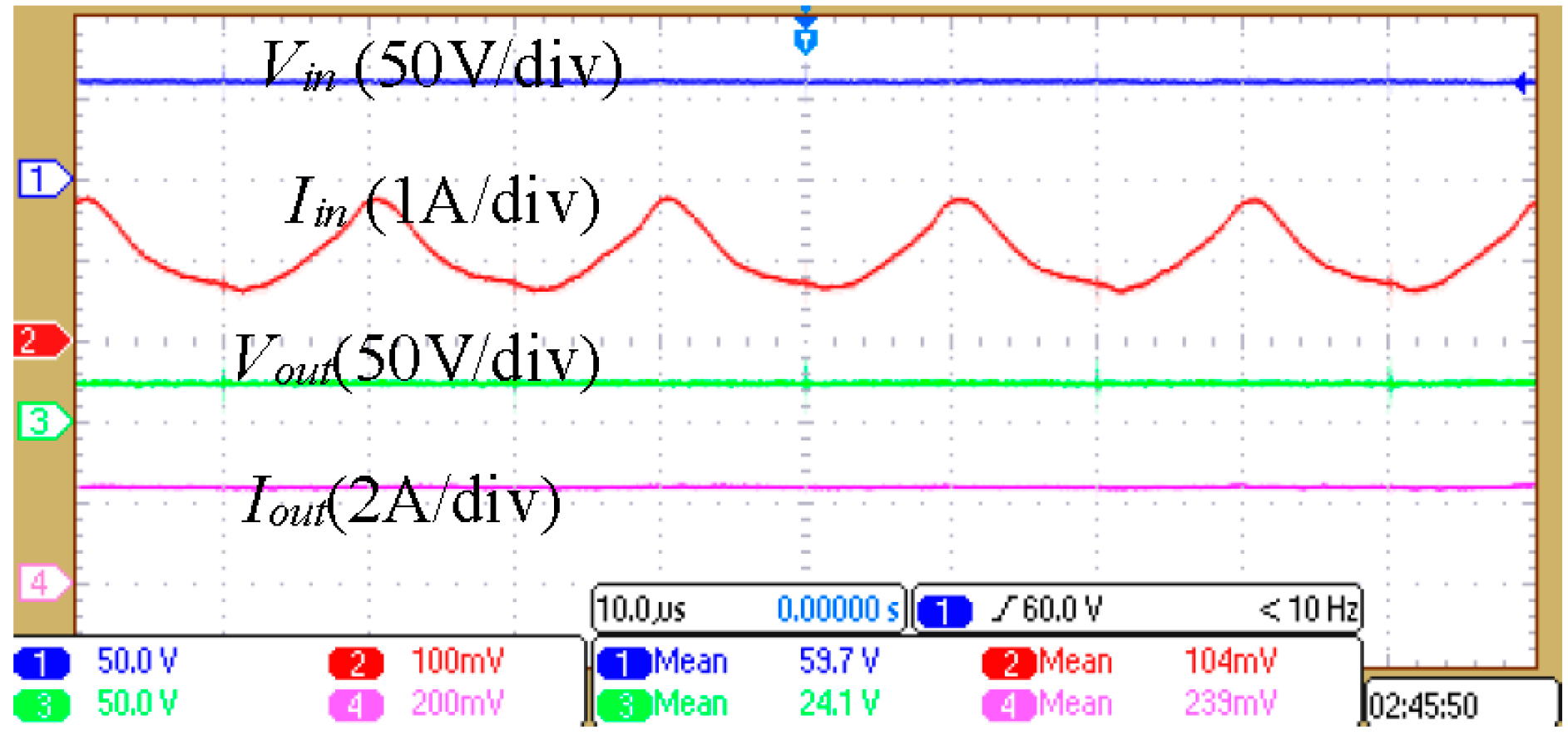
| Parameter | Boost | Buck | Flyback |
|---|---|---|---|
| Vin | 19.3 V | 60 V | 12.1 V |
| Iin | 3.18 A | 1.04 A | 0.434 A |
| Vout | 75.2 V | 24.1 V | 25.7 V |
| Iout | 0.794 A | 2.39 A | 0.151 A |
| Δi | 1.1 A | 2.95 A | 0.89 A |
| fsw | 50 KHz | 50 KHz | 100 KHz |
| D | 0.75 | 0.4 | 0.7 |
| ESR | 0.603 Ω | 0.603 Ω | 0.603 Ω |
| VD0 | 1 V | 1 V | 1 V |
| RD | 7 mΩ | 7 mΩ | 7 mΩ |
| DCR/Rpri | 0.06 Ω | 34 mΩ | 0.09 |
| ACR/Rsec | 0 | 1.5 Ω | 0.58 |
| Qrr | 195 nC | 195 nC | 195 nC |
| Qgs | 64 nC | 13 nC | 13 nC |
| RDSon | 0.029 Ω | 0.18 Ω | 0.18 Ω |
| tr | 100 nsec | 51 nsec | 51 nsec |
| tf | 63 nsec | 36 nsec | 36 nsec |
| ≈Rc | 3325 Ω | - | - |
| Lm, Lpri | - | - | 59.4 µH, 3.5 µH |
| B | - | 3400 mT | 42.42 mT |
| Ve/AC | - | 0.24 cm3 | 0.97 cm3 |
| Duty Ratio | PMeasured (W) | PEstimated (W) | Error % |
|---|---|---|---|
| 30% | 0.6 | 0.56 | −6.6% |
| 40% | 0.78 | 0.72 | −7.69% |
| 50% | 0.97 | 0.92 | −5.15% |
| 60% | 1.36 | 1.37 | 0.74% |
| Duty Ratio | PMeasured (W) | PEstimated (W) | Error % |
|---|---|---|---|
| 20% | 2.54 | 2.49 | −1.96% |
| 30% | 3.76 | 3.78 | 0.53% |
| 40% | 4.8 | 5.04 | 5% |
| 50% | 7.05 | 6.55 | −7.09% |
| Duty Ratio | PMeasured (W) | PEstimated (W) | Error % |
|---|---|---|---|
| 20% | 0.32 | 0.31 | −3.13% |
| 30% | 0.55 | 0.56 | 1.81% |
| 40% | 0.85 | 0.82 | −4.7% |
| 50% | 1.32 | 1.27 | −3.78% |
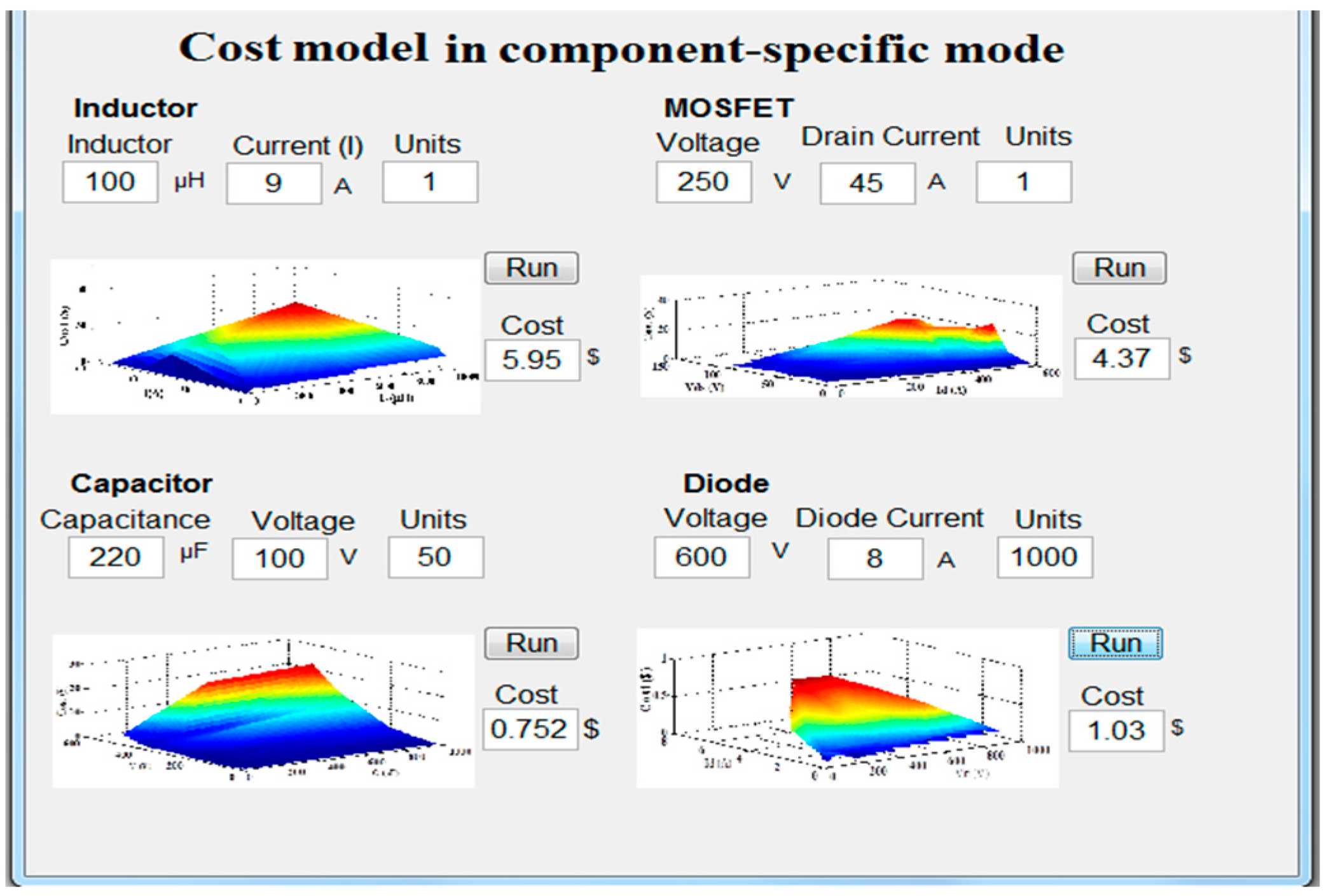
| Component | Actual Cost | Estimated Cost | Error % |
|---|---|---|---|
| MOSFET (IRFP4332PBF) | $4.33 | $4.37 | −0.92% |
| Inductor (AIRD-03-101K) | $5.97 | $5.95 | 0.33% |
| Diode (MURF860G) | $0.99 | $1.03 | −4.04% |
| Capacitor (EEU-EB2D221) | $0.723 | $0.752 | −4.01% |
| Core (B66421G0000X187) | $0.69 | $0.724 | −4.93% |
| Wire (Belden 22AWG) | $49.03 | $48.03 | 2.039% |
| MOSFET | Diode | ||
|---|---|---|---|
| Suitable Components | PLoss (W) | Suitable Components | PLoss (W) |
| FQD4N20TMFSCT-ND | 5.03508831 | ||
| FQD4N20TMFSDKRND | 5.03508831 | SK35A-LTP | 2.878 |
| Capacitor | STPS5H100B-TR | 2.037 | |
| Suitable Components | PLoss (W) | B350A-13-F | 2.881 |
| UHE2A101MPD | 0.005741826 | SS35 | 2.877 |
| ESH107M200AM7AA | 1.07828776 | CDBC5100-G | 2.464 |
| UVZ2F101MHD | 0.014467593 | SB550-E3/54 | 2.397 |
| UPT2G101MHD6 | 0.014467593 | SK55L-TP | 2.464 |
| Inductor | SB550 | 2.255 | |
| Suitable Components | PLoss (W) | CDBC580-G | 2.458 |
| PCV-0-104-01L | 0.940523683 | SS5P10-M3/86A | 2.301 |
| PCV-0-104-03L | 0.35827212 | SB580-T | 2.213 |
| PCV-0-104-05L | 0.274278036 | HSM580G/TR13 | 2.464 |
| RGP30B-E3/73 | 3.186 | ||
| SK310A-LTP | 2.890 | ||
| CDBA3100-G | 2.734 | ||
| B3100-13-F | 2.586 | ||
| MOSFET | Capacitor | ||
|---|---|---|---|
| Suitable Components | PLoss (W) | Suitable Components | PLoss (W) |
| RDN100N20FU6-ND | 3.436527778 | EEU-EB2D221 | 0.000223251 |
| RDN100N20-ND | 3.436527778 | LGU2F221MELB | 0.000223251 |
| IRLI640GPBF | 1.898888889 | ECO-S2GB221EA | 0.0271 |
| IRLI640G | 1.898888889 | Inductor | |
| FQP9N30 | 4.466997222 | Suitable Components | PLoss (W) |
| STP12NK30Z 3.763864198 | 3.76386 | PCV-0-274-10L | 2.983 |
| Diode | PCV-2-274-03L | 3.3021 | |
| PCV-2-274-05L | |||
| PCV-2-274-10L | |||
| PCV-2-394-05L | |||
| Suitable Components | PLoss (W) | PCV-2-274-05L | 1.172 |
| CDBB5200-HF | 1.495 | PCV-2-274-10L | 1.528 |
| PCV-2-394-05L | 3.299 | ||
| MOSFET | Diode | ||
|---|---|---|---|
| Suitable Components | Cost ($) | Suitable Components | Cost ($) |
| FQD4N20TMFSCT-ND | 0.67 | SK35A-LTP | 0.57 |
| FQD4N20TMFSDKR-ND | 0.67 | STPS5H100B-TR | 1.4 |
| Capacitor | B350A-13-F | 0.46 | |
| Suitable Components | Cost ($) | SS35 | 0.63 |
| UHE2A101MPD | 0.56 | B550C-13-F | 0.95 |
| ESH107M200AM7AA | 1.02 | SB550-E3/54 | 0.61 |
| UVZ2F101MHD | 1.85 | SK55L-TP | 0.49 |
| UPT2G101MHD6 | 2.68 | SB550 | 0.56 |
| Inductor | CDBC580-G | 0.74 | |
| Suitable Components | Cost ($) | SB580 | 0.59 |
| PCV-0-104-01L | 1.31 | SB580-T | 0.43 |
| PCV-0-104-03L | 1.48 | HSM580G/TR13 | 1.34 |
| PCV-0-104-05L | 2.37 | RGP30B-E3/73 | 0.476 |
| SK310A-LTP | 0.57 | ||
| CDBA3100-G | 0.63 | ||
| B3100-13-F | 0.68 | ||
| CDBC5100-G | 0.74 | ||
| SS5P10-M3/86A | 0.77 | ||
| SB5100-T | 0.74 | ||
| MOSFET | ||
|---|---|---|
| Suitable Components | Cost ($) | PLoss (W) |
| RDN100N20FU6-ND | 2.73 | 3.436 |
| RDN100N20-ND | 2.73 | 3.436 |
| IRLI640GPBF | 2.88 | 1.898 |
| IRLI640G | 2.88 | 1.898 |
| FQP9N30 | 1.18 | 4.467 |
| STP12NK30Z | 1.95 | 3.763864198 |
| Diode | ||
| Suitable Components | Cost ($) | PLoss (W) |
| CDBB5200-HF | 0.21 | 1.495 |
| Inductor | ||
| Suitable Components | Cost ($) | PLoss (W) |
| PCV-0-274-10L | 4.08 | 2.984 |
| PCV-2-274-03L | ||
| PCV-2-274-05L | ||
| PCV-2-274-10L | ||
| PCV-2-394-05L | ||
| PCV-2-274-03L | 4.15 | 3.302 |
| PCV-2-274-05L | 4.56 | 1.172 |
| PCV-2-274-10L | 7.39 | 1.528 |
| PCV-2-394-05L | 5.1 | 3.299 |
| Capacitor | ||
| Suitable Components | Cost ($) | PLoss (W) |
| EEU-EB2D221 | 2.56 | 0.000223251 |
| LGU2F221MELB | 7.022 | 0.000223251 |
| ECO-S2GB221EA | 4.68 | 0.0271 |
© 2016 by the authors; licensee MDPI, Basel, Switzerland. This article is an open access article distributed under the terms and conditions of the Creative Commons Attribution (CC-BY) license (http://creativecommons.org/licenses/by/4.0/).
Share and Cite
Kulkarni, A.V.; Chen, W.; Bazzi, A.M. Implementation of Rapid Prototyping Tools for Power Loss and Cost Minimization of DC-DC Converters. Energies 2016, 9, 509. https://doi.org/10.3390/en9070509
Kulkarni AV, Chen W, Bazzi AM. Implementation of Rapid Prototyping Tools for Power Loss and Cost Minimization of DC-DC Converters. Energies. 2016; 9(7):509. https://doi.org/10.3390/en9070509
Chicago/Turabian StyleKulkarni, Amruta V., Weiqiang Chen, and Ali M. Bazzi. 2016. "Implementation of Rapid Prototyping Tools for Power Loss and Cost Minimization of DC-DC Converters" Energies 9, no. 7: 509. https://doi.org/10.3390/en9070509