Article

High Stable, Transparent and Conductive ZnO/Ag/ZnO Nanofilm Electrodes on Rigid/Flexible Substrates

1
Key Laboratory for Organic Electronics & Information Displays (KLOEID), Synergetic Innovation Center for Organic Electronics and Information Displays (SICOEID), Institute of Advanced Materials (IAM), School of Materials Science and Engineering (SMSE), Nanjing University of Posts and Telecommunications (NUPT), Nanjing 210023, China
2
School of Science, Nanjing University of Posts and Telecommunications (NUPT), Nanjing 210023, China
*
Authors to whom correspondence should be addressed.
Energies 2016, 9(6), 443; https://doi.org/10.3390/en9060443
Submission received: 17 March 2016 / Revised: 16 May 2016 / Accepted: 16 May 2016 / Published: 8 June 2016
(This article belongs to the Special Issue Nano-Structured Solar Cells)

Abstract

:
Here, highly transparent, conductive, and stable ZnO/Ag/ZnO electrodes on transparent rigid glass and flexible substrates were prepared by facile, room-temperature magnetron sputtering, in which the continuous Ag layers were obtained by means of oxidization-induced effect under an Ar atmosphere with tiny amounts of O2. The results showed an appropriate amount of O2 was beneficial to form continuous Ag films because of the adsorption of oxygen between the ZnO and Ag layers. When the concentration of O2 in the Ar atmosphere was 2.0%–3.0%, ZnO (40 nm)/Ag (10 nm)/ZnO (40 nm) films on rigid glass showed visible-range transmittance of 94.8% and sheet resistance of 8.58 Ω·sq−1, while the corresponding data on flexible PET substrates were 95.9% and 8.11 Ω·sq−1, respectively. In addition, the outstanding electrodes remained stable for more than six months under air conditioned conditions. The electrodes are fully functional as universal rigid/flexible electrodes for high-performance electronic applications.

Graphical Abstract

1. Introduction

Conductivity and transmittance profoundly affect the performance of transparent conductive electrode-based optoelectronic devices, such as organic light emitting diodes (LEDs), photovoltaic cells, light-emitting diodes, etc. [1,2,3]. Nowadays, the most common electrode material is indium-doped tin oxide (ITO) film, in which the transmittance is 90% and the sheet resistance is about 10 Ω·sq−1 on glass prepared at a high temperature (about 300 °C). However, on flexible substrates, the sheet resistance is larger than 40–200 Ω·sq−1 when prepared at room temperature [4]. Moreover, the high-cost of indium is a drawback for low-cost electronic devices. Therefore, pursuing ideal high transparent and conductive, low-cost electrodes to replace ITO on rigid and flexible substrates has become an essential objective for next generation optoelectronic devices.
Nowadays, several alternative transparent electrodes have been reported, such as carbon nanotubes [5,6], grapheme [7,8], doped ZnO conducting films [9,10], conducting polymes [11,12], metal materials [13,14], etc. Currently, Ag nanomaterial is regarded as one of the most appealing transparent electrodes due to its excellent conductivity. However, Ag nanomaterial has poor optical transmittance. Furthermore, Ag nanomaterial cannot stay stable for a long time when exposed to air. To overcome these shortcomings, dielectric/Ag/dielectric multilayer structures have been proposed, which possess the characteristics of high conductivity and stability [15,16,17]. However, dielectric/Ag/dielectric films have poor visible-light transmittance compared with those of alternative electrodes, such as the ZnO/Ag/ZnO films with less than 90% visible-light transmittance [18,19].
Herein, Ag nanofilms were formed continuously by the oxidization-induced effect in ZnO/Ag/ZnO multilayers on glass and PET substrates by room-temperature magnetron sputtering under an Ar atmosphere with a tiny amount O2. First, the influence of the concentration of flowing O2 on the transmittance and conductivity was characterized and discussed. Then, the deposition time of ZnO and Ag layers has been investigated to get the optimal sputtering parameters for optical and electrical properties. The study showed that the ZnO (40 nm)/Ag (10 nm)/ZnO (40 nm) films achieved high optical transmittance of 94.8% and low sheet resistance of 8.58 Ω·sq−1 on rigid transparent glass, and optical transmittance of 95.9% and low sheet resistance of 8.11 Ω·sq−1 on flexible PET substrate when the O2 ratio was 3.0% relative to the Ar content. Meanwhile, the ZnO films absorb ultraviolet (UV) light, resulting in UV protection of the ZnO/Ag/ZnO electrodes, which can be applied the UV-damped photoelectric devices, such as perovskite solar cells [20,21]. Moreover, the above electrodes show perfect stability over six months under an air atmosphere. The ideal ZnO/Ag/ZnO transparent electrode with continuous Ag films on rigid/flexible substrates will greatly broaden the applications for enhanced-performance transparent conductive electrode-based optoelectronic devices.

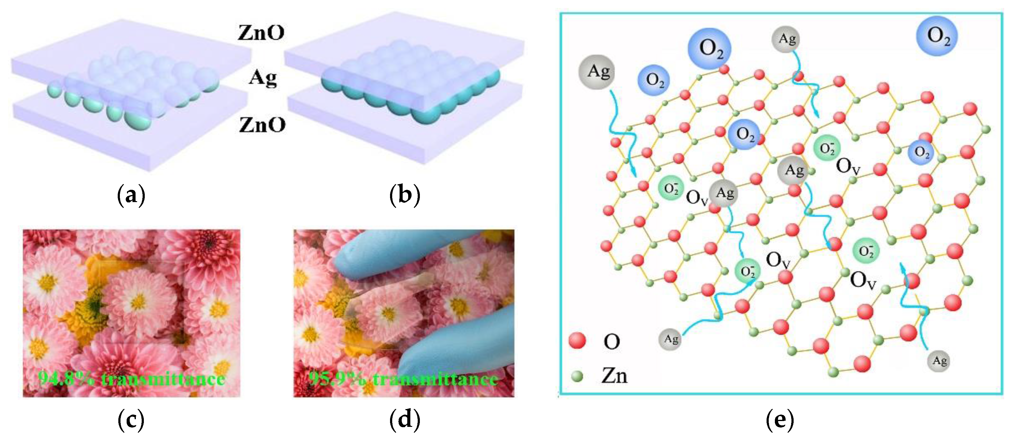
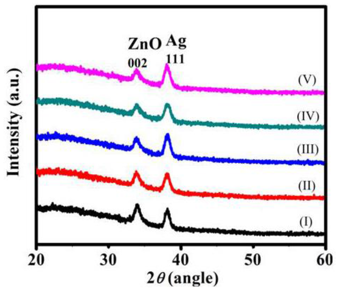
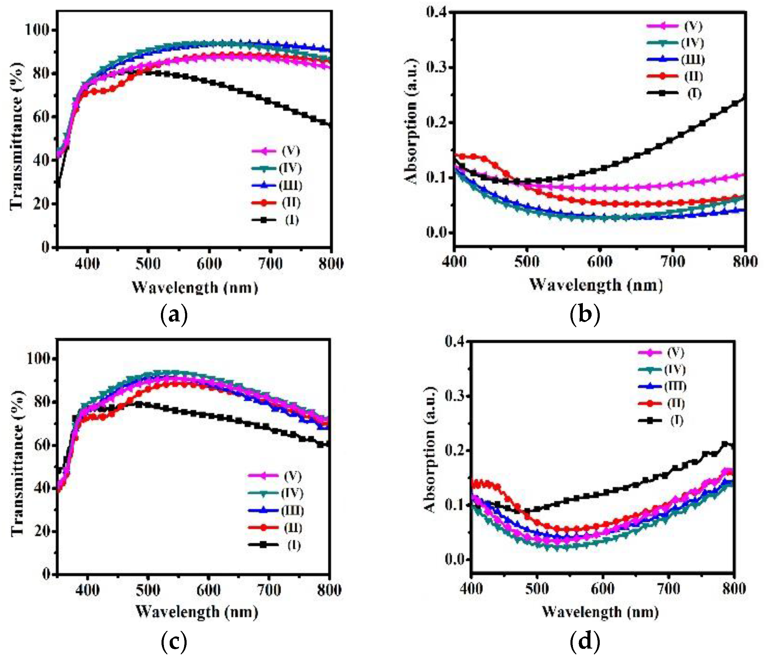
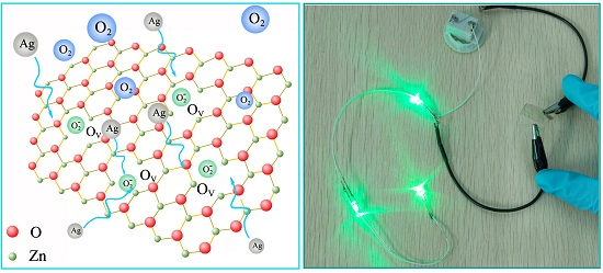
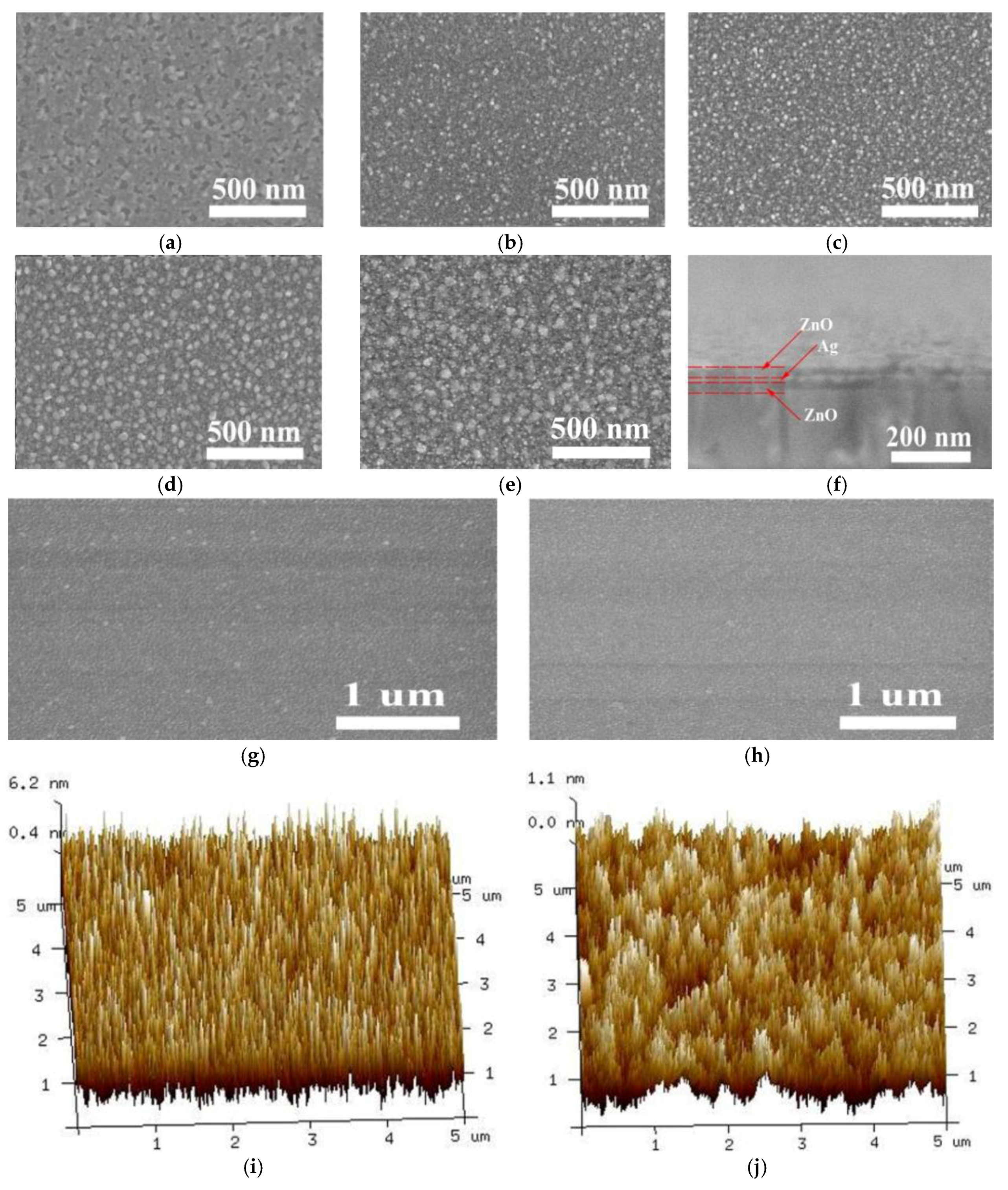
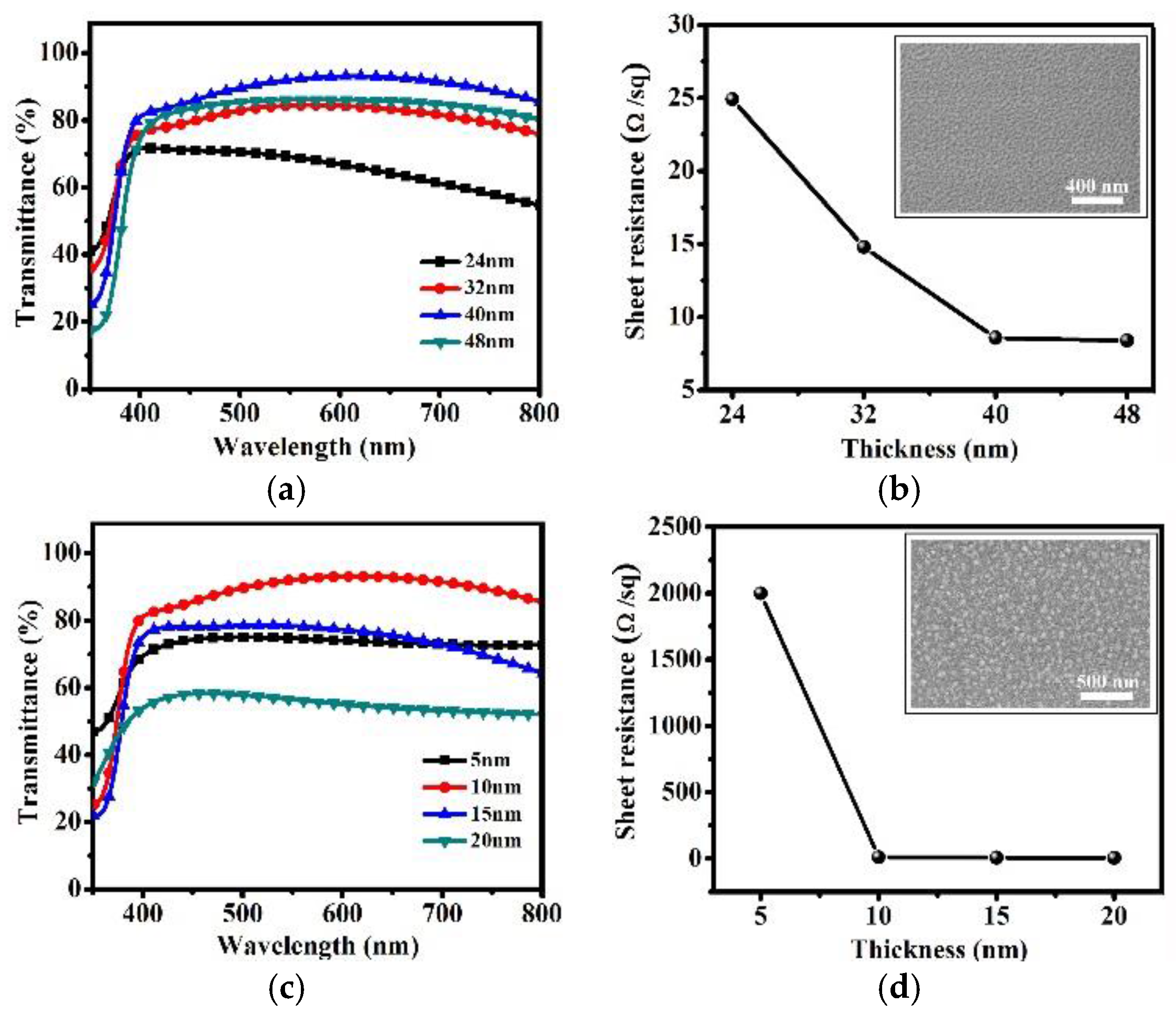
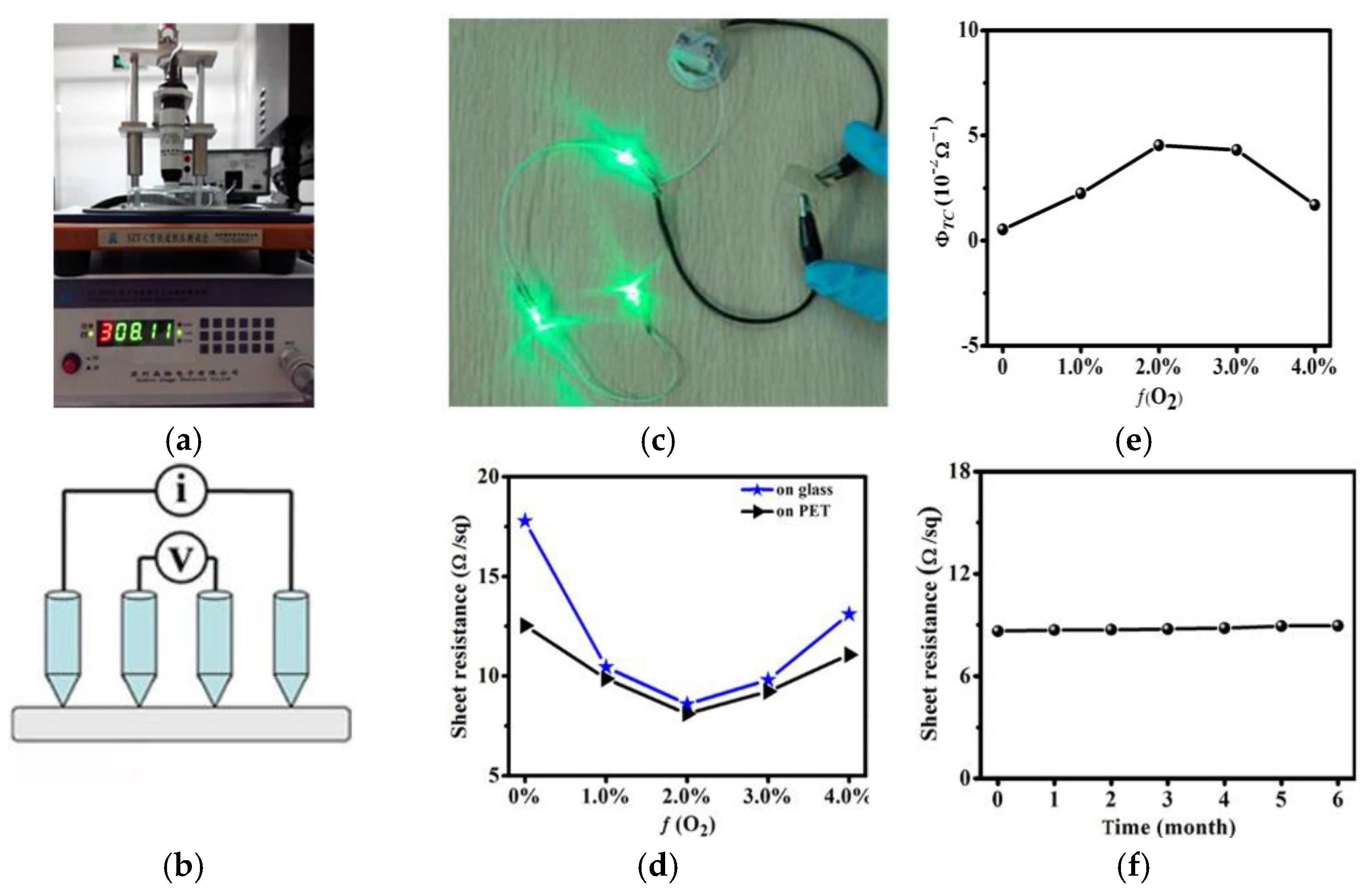
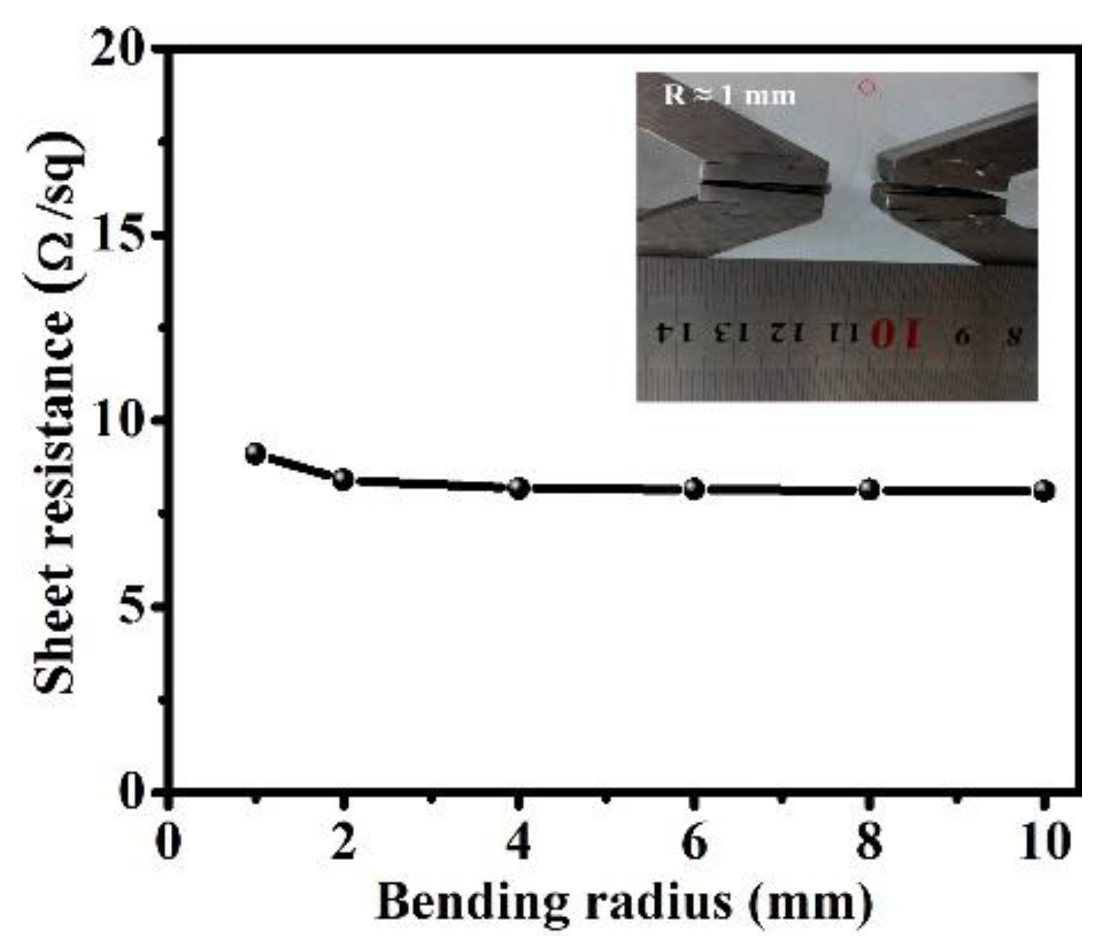
2. Results and Discussion

Figure 1a,b shows schematic diagrams of ZnO/Ag/ZnO films with discontinuous and continuous Ag films, respectively. In Figure 1a, the Ag film is discontinuous inserted between both ZnO layers when the deposition of Ag was performed in the absence of O2. When a percentage of O2 in Ar atmosphere was introduced during the deposition of Ag, the O atoms guide the Ag to form a continuous film and evenly deposit on the ZnO film, where the guiding force results from the strong interaction of oxygen between Ag and ZnO layers. As the schematic diagram in Figure 1b shows, the morphology of the Ag film is continuous under the oxidation-induced effect, and the continuous Ag film favors light transmission and charge transfer. The obtained ZnO/Ag/ZnO films on rigid glass and flexible PET substrates, which exhibit outstanding transparency, are pictured in Figure 1c,d, respectively. The phenomenon where the oxygen does not penetrate through the Ag layer and attaches itself to the ZnO surface, while the arriving Ag atoms are adsorbed independently and rearrange because of the adsorption of oxygen between ZnO and Ag layers, as shown in Figure 1e, was illustrated by Wüstner [22].
Figure 2 indicates the X-ray diffraction (XRD) patterns that verify the phase of ZnO/Ag/ZnO films. The peaks at 33° was assigned to the (002) plane of ZnO (JCPDS No. 36-1451) and the obvious peaks at 38° correspond to the (111) plane of the Ag phase (JCPDS No. 87-0597). It is worthwhile to note that there were no peak impurities besides the ZnO and Ag phases. Consequently, pure Ag can be successfully deposited on a ZnO layer even though there was little O2 in the Ar atmosphere.
The morphology of the Ag layers deposited on a bottom ZnO layer at different concentrations of O2 in the Ar atmosphere was observed by scanning electron microscope (SEM) technology, as shown in Figure 3a–e. The O2 concentration greatly affected the morphology of the Ag films. If O2 was absent from the Ar atmosphere, the morphology of the Ag film was not completely continuous. In the presence of a percentage of O2 in the Ar atmosphere, the Ag particles get together and form continuous films on the ZnO layer because of the adsorption of oxygen. When the concentration of O2 was 3%, the morphology of the Ag film was completely continuous. However, too much O2 absorbed more Ag leading to much larger Ag particles that overlap together, such as seen in Figure 3e for a 4% concentration of O2. Figure 3f shows the cross-sectional views of SEM images of a ZnO/Ag/ZnO multilayer grown on the ITO substrate, where the Ag film was continuous.
The morphology of the Ag layer would influence the upper layer of ZnO, which was characterized by SEM and atomic force microscope (AFM) technologies. Figure 3g,h displays images of top ZnO thin films on Ag/ZnO surfaces (f(O2) = 0 and f(O2) = 3.0%, respectively). The ZnO film on the Ag/ZnO (f(O2) = 0%) was very rough, because of the resulting discontinuous Ag film. The superior morphology of the top ZnO films on Ag/ZnO (f(O2) = 3.0%) was more smooth because of the more continuous Ag films. To further illustrate the morphology of ZnO/Ag/ZnO films, AFM measurements were carried out to reveal clear differences in the roughness of the surface topography, as shown in Figure 3i,j. The root mean square (RMS) roughness was calculated as 1.66 nm and 0.365 nm for ZnO/Ag/ZnO (f(O2) = 0%) and ZnO/Ag/ZnO (f(O2) = 3.0%), respectively. The differences of smoothness between the ZnO films could be primarily explained by influences of the discontinuity and granularity states of the Ag films on the bottom ZnO morphologies, which corresponded to the SEM morphology mentioned above.
For optimal structures, the effect of the thickness of ZnO and Ag layers on optical transmittance and electrical conductivity of ZnO/Ag/ZnO electrodes was investigated. Herein, the thickness of the ZnO film was varied from 24 nm to 48 nm by controlling the sputtering time. As it can be seen from Figure 4a,b, up to the film thickness of 40 nm, the optical transmittance and electrical conductivity of multilayer films increases with the thickness of ZnO which the maximum transmittance, 94.8% at λ = 560 nm, the minimum sheet resistance, 8.58 Ω·sq−1, are achieved with thickness of 40 nm. The main reason is that the 40 nm ZnO layer has been completely formed continuous and smooth film as shown the inserted picture in Figure 4b. When the film thickness increases to 48 nm, a slight decrease occurs in the transmittance respect. Figure 4c shows the transmittance as a function of the Ag interfacial layer for thicknesses varying from 5 nm to 20 nm, while the thicknesses of both bottom and top ZnO films are kept constant at 40 nm. At a thickness of 5 nm, the Ag film is discontinuous, giving a no optimized antireflection effect, more scattering, and plasmonic absorption [23]. With 10 nm thickness of Ag, the ZnO/Ag/ZnO transparent electrode shows maximum transmittance in that the interfacial layer changes from islands to continuous films as shown in the insert in Figure 4d. For thicknesses >10 nm, the transmittance shows an abrupt decrease that attenuates the effects of the morphology improvements. On the other hand, the sheet resistance shows the largest drop when the thickness varies from 5 nm to 10 nm as shown in Figure 4d. Based on these results, the optimized thicknesses of the ZnO and Ag layers were 40 nm and 10 nm, respectively.
The transparency is a vital factor for a transparent electrode. It was obvious that the transmittances in the stacked ZnO/Ag/ZnO multilayer are strongly affected by the morphology of the Ag layer which is due to the O2 concentration. Figure 5a shows the optical transmittance of ZnO/Ag/ZnO electrode deposited on glass at different f(O2) from 0% to 4.0%.
If O2 was absent during Ag deposition, the obtained ZnO/Ag/ZnO electrode on transparent glass had poor optical transmittance (less than 80% in 350–800 nm). When an appropriate amount of O2 was used in the Ag deposition, the optical transmittance of the ZnO/Ag/ZnO electrodes was obviously improved. In particular, when the O2 concentration was 3%, the optical transmittance reached a superlative value of 94.8% at the wavelength of 560 nm, consistent with the SEM and AFM results. Meanwhile, the transmittances are not more than 40% in the wavelength range of 300–400 nm which indicated that the ZnO/Ag/ZnO system can be viewed as a UV-protected electrode for optoelectronic devices [20].
The corresponding absorption spectra in visible wavelengths for ZnO/Ag/ZnO films for different f(O2) values are shown in Figure 5b. The absorption value was the largest if there was no O2 during the Ag deposition, while the value was the smallest when the O2 concentration was 3%. The representation further confirmed our results whereby the continuous Ag film provides excellent optical transmittance. The transparent flexible electrode of the ZnO/Ag/ZnO films on PET substrate gave the same result again, as shown in Figure 5c,d. The electrode of 3.0% O2 under optimized conditions shows a transmittance of 95.9% at a wavelength of 570 nm.
The conductivity of the electrodes on transparent rigid glass and flexible PET substrates are characterized by the four point probe technology in Figure 6a and the schematic diagrams of the four-point probe system used to measure the sheet resistance is shown in Figure 6b [24]. In Figure 6c, the ZnO/Ag/ZnO flexible electrode (Rs = 9.23 Ω·sq−1, T = 94.2%) can replace electric wire to complete the circuit and enable light-emission from a LED, demonstrating its high conductivity. As illustrated in Figure 6d, on the rigid glass substrate, the sheet resistance decreased from 17.54 Ω·sq−1 to 8.58 Ω·sq−1 when the f(O2) ranged from 0% to 2.0%. The conductivity was greatly improved based on the continuous Ag film formed by oxidation-induced deposition on the ZnO layer. However, when the O2 concentration was over 3.0%, there was slight increment in the sheet resistance. The ZnO/Ag/ZnO films deposited on PET substrate has the same sheet resistance trend from 12.57 Ω·sq1 (f(O2) = 0) to 8.11 Ω·sq−1 (f(O2) = 2.0%), then to 11.07 Ω·sq−1 (f(O2) = 4.0%). Importantly, we obtained a low sheet resistance 8.11 Ω·sq−1 for ZnO/Ag/ZnO flexible electrodes, which is outstanding in the field of transparent flexible electrodes [25,26,27].
The figure of merit (ΦTC) is an important parameter to evaluate the performance of transparent electrodes, which was defined by Haacke as follows [28]:
Φ T C = T 10 / R S
where T is the optical transmittance at a wavelength of 550 nm and RS is the sheet resistance. ΦTC was calculated as shown in Figure 6e, as was as high as 4.53 × 10⁻² Ω−1 when the f(O2) was 2.0%, matching well the foregoing results. The ΦTC of ZnO/Ag/ZnO is higher than the reported value (0.88 × 10⁻²) of ITO [29]. The result indicates that highly transparent and conductive ZnO/Ag/ZnO can be prepared by the inclusion of a remarkably small amount of oxygen while the Ag films are deposited. The ZnO layer in ZnO/Ag/ZnO electrodes also prevents the oxidation of Ag to enhance the stability for long-life flexible electronics. We investigated how the sheet resistance changed under an air atomsphere with the exposure time, as shown Figure 6f. After six months, the electrical performance of ZnO/Ag/ZnO (f(O2) = 2.0%) electrode was still perfect.
The structural durability of ZnO/Ag/ZnO (f(O2) = 2.0%) multilayer on flexible PET was characterized by a bending test under tensile stress. Figure 7 shows the sheet resistance of ZnO/Ag/ZnO electrode bent 800 times under different bending radii from 1 nm to 10 mm. When the bending radius is less than 2 mm, the resistance after 800 bending repetitions almost remained constant as before bending. When the bending radius was 2 mm, the sheet resistance increased only about 0.5 Ω after 800 bending cycles. The sheet resistance did not change significantly even when the bending radius decreased to 1 mm. The insert picture is a bending test of ZnO/Ag/ZnO multilayer on PET for 1 mm bending radius. This means that the ZnO/Ag/ZnO (f(O2) = 2.0%) multilayer on flexible PET has excellent flexibility due to the existence of the Ag metal layer.

3. Materials and Methods

3.1. Fabrication of ZnO/Ag/ZnO Films

The ZnO/Ag/ZnO transparent electrodes on glass and PET substrates were deposited using a tilted dual-target radio frequency (RF) and direct current (DC) magnetron sputtering system (TSU-450, Techno, Beijing, China) at room temperature. The glass and PET substrates were ultrasonically cleaned in deionized water, acetone and ethanol for 15 min, respectively, followed by drying under flowing N2. For preparing the electrodes, the pressure in the chamber was pumped down to <8 × 10⁻⁴ Pa, while the working pressure was set at 2.0 Pa. Before deposition, the ZnO and Ag targets were all systematically pre-sputtered during 15 min under a pure Ar atmosphere. Both ZnO films were deposited with a RF power of 100 W from ZnO target (99.9% pure). The Ag films were obtained from 99.99% purity Ag under Ar atmospheres with different ratios of O2 {f(O2): (O2/(O2 + Ar) (I) 0; (II) 1.0%; (III) 2.0%; (IV) 3.0%; (V) 4.0%)} with a DC power of 20 W. The thicknesses of the ZnO and Ag layer were controlled by the sputtering time. Table 1 shows the experimental conditions for the deposition of ZnO/Ag/ZnO multilayers.

3.2. Characterization

The crystal structure of ZnO/Ag/ZnO films was investigated using XRD (D8 ADVANCE, Bruker, Karlsruhe, Germany) with Cu-Kα (λ = 0.15405 nm) radiation. The surface morphology of the Ag films was characterized by using SEM (S-4800, Hitachi, Tokyo, Japan) and atomic force microscopy (AFM, XE-100, Park System, Tokyo, Japan). The thickness of the films was checked by quartz crystal thickness monitor (Dektak XT, Bruker). The transmittance of ZnO/Ag/ZnO electrodes was measured using a UV/visible spectrometer (Lambda 35, PerkinElmer, Waltham, MA, USA). The sheet resistance of the ZnO/Ag/ZnO electrodes was analyzed by a four-point probe (ST-2258A, Suzhou lattice Electronics Co., Ltd., Suzhou, China). The structural durability of the ZnO/Ag/ZnO on PET was evaluated by bending test using an electronic tensile testing machine (CMT-6304, Zhuhai Sust Electrical Equipment Co., Ltd., Zhuhai, China).

4. Conclusions

In summary, we have developed highly stable, transparent and conductive ZnO/Ag/ZnO electrodes on arbitrary transparent substrates, such as glass and PET, by a simple and room-temperature magnetron sputtering method under an Ar atmosphere containing an appropriate amount of O2 to prepare continuous Ag films. Our studies have shown that O2 flows with concentrations between 2% and 3% could greatly induce the growth of Ag films, which is very good for the transmittance and conductivity of ZnO/Ag/ZnO electrodes. The best performance based on ZnO/Ag/ZnO electrodes achieved 94.8% visible transmittance, 8.58 Ω·sq−1 on transparent glass, and 95.9% visible transmittance, 8.11 Ω·sq−1 on PET substrate. The UV-protective properties of the ZnO/Ag/ZnO electrodes could be readily applied to UV-damped photoelectric devices. Importantly, the above electrodes indicated good stability after six months under an air atmosphere. We believe that the high-performance ZnO/Ag/ZnO electrodes with continuous Ag film on rigid/flexible transparent substrates will greatly broaden the applications of enhanced-performance transparent conductive electrode-based optoelectronic devices.

Acknowledgments

We acknowledge the financial support from the National Basic Research Program of China (2012CB933301 and 2014CB648300), the Ministry of Education of China (No. IRT1148), the National Synergistic Innovation Center for Advanced Materials (SICAM), the Natural Science Foundation of Jiangsu Province of China (BM2012010), the Project Funded by the Priority Academic Program Development of Jiangsu Higher Education Institutions (YX03001), and the National Natural Science Foundation of China (51172110 and 51372119).

Author Contributions

Qiaoxia Zhang has carried out most of the work presented in this paper; Yanghua Zhao and Zhenhong Jia performed the experiments; Zhengfei Qin analyzed the data; Liang Chu, Jian Zhang and Jingping Yang assisted in the manuscript modification; Wei Huang and Xing’ao Li provided the financial and technical support for designing and conducting the research, as well as supervised the whole research process.

Conflicts of Interest

The authors declare no conflict of interest.

References

  1. Zadsar, M.; Fallah, H.R.; Mahmoodzadeh, M.H.; Tabatabaei, S.V. The effect of Ag layer thickness on the properties of WO3/Ag/MoO3 multilayer films as anode in organic light emitting diodes. J. Lumin. 2012, 132, 992–997. [Google Scholar] [CrossRef]
  2. Kim, Y.H.; Kim, J.S.; Kim, W.M.; Seong, T.Y.; Lee, J.; Müller-Meskamp, L.; Leo, K. Realizing the potential of ZnO with alternative nonmetallic Co-dopants as electrode materials for small molecule optoelectronic devices. Adv. Funct. Mater. 2013, 23, 3645–3652. [Google Scholar] [CrossRef]
  3. Ye, S.; Rathmell, A.R.; Stewart, I.E.; Ha, Y.C.; Wilson, A.R.; Chen, Z.; Wiley, B.J. A rapid synthesis of high aspect ratio copper nanowires for high-performance transparent conducting films. Chem. Commun. 2014, 50, 2562–2564. [Google Scholar] [CrossRef] [PubMed]
  4. Ham, J.; Kim, S.; Jung, G.H.; Dong, W.J.; Lee, J.-L. Design of broadband transparent electrodes for flexible organic solar cells. J. Mater. Chem. A 2013, 1, 3076–3082. [Google Scholar] [CrossRef]
  5. Tenent, R.C.; Barnes, T.M.; Bergeson, J.D.; Ferguson, A.J.; To, B.; Gedvilas, L.M.; Heben, M.J.; Blackburn, J.L. Ultrasmooth, large-area, high-uniformity, conductive transparent single-walled-carbon-nanotube films for photovoltaics produced by ultrasonic spraying. Adv. Mater. 2009, 21, 3210–3216. [Google Scholar] [CrossRef]
  6. Hellstrom, S.L.; Vosgueritchian, M.; Stoltenberg, R.M.; Irfan, I.; Hammock, M.; Wang, Y.B.; Jia, C.; Guo, X.; Gao, Y.; Bao, Z. Strong and stable doping of carbon nanotubes and graphene by MoOx for transparent electrodes. Nano Lett. 2012, 12, 3574–3580. [Google Scholar] [CrossRef] [PubMed]
  7. Ahn, Y.; Lee, D.; Lee, Y. Copper nanowire-graphene core-shell nanostructure for highly stable transparent conducting electrodes. ACS Nano 2015, 9, 3125–3133. [Google Scholar] [CrossRef] [PubMed]
  8. Kahng, Y.H.; Kim, M.-K.; Lee, J.-H.; Kim, Y.J.; Kim, N.; Park, D.-W.; Lee, K. Highly conductive flexible transparent electrodes fabricated by combining graphene films and inkjet-printed silver grids. Sol. Energy Mater. Sol. Cells 2014, 124, 86–91. [Google Scholar] [CrossRef]
  9. Lei, P.-H.; Hsu, C.-M.; Fan, Y.-S. Flexible organic light-emitting diodes on a polyestersulfone (PES) substrate using Al-doped ZnO anode grown by dual-plasma-enhanced metalorganic deposition system. Org. Electron. 2013, 14, 236–249. [Google Scholar] [CrossRef]
  10. Duan, L.; Wang, P.; Yu, X.; Han, X.; Chen, Y.; Zhao, P.; Li, D.; Yao, R. The synthesis and characterization of Ag–N dual-doped p-type ZnO: Experiment and theory. Phys. Chem. Chem. Phys. 2014, 16, 4092–4097. [Google Scholar] [CrossRef] [PubMed]
  11. Vosgueritchian, M.; Lipomi, D.J.; Bao, Z. Highly conductive and transparent PEDOT: PSS films with a fluorosurfactant for stretchable and flexible transparent electrodes. Adv. Funct. Mater. 2012, 22, 421–428. [Google Scholar] [CrossRef]
  12. Zhang, W.F.; Zhao, B.F.; He, Z.C.; Zhao, X.M.; Wang, H.T.; Yang, S.F.; Wu, H.B.; Cao, Y. High-efficiency ITO-free polymer solar cells using highly conductive PEDOT:PSS/surfactant bilayer transparent anodes. Energy Environ. Sci. 2013, 6, 1956–1964. [Google Scholar] [CrossRef]
  13. Feng, J.; Hong, Y.; Zhang, J.; Wang, P.; Hu, Z.; Wang, Q.; Han, L.; Zhu, Y. Novel core-shell TiO2 microsphere scattering layer, with superior surface area and scattering properties, shows superior performance in dye-sensitized solar cells. J. Mater. Chem. A 2014, 2, 1502–1508. [Google Scholar] [CrossRef]
  14. Koo, J.-R.; Lee, S.J.; Lee, H.W.; Lee, D.H.; Yang, H.J.; Kim, W.Y.; Kim, Y.K. Flexible bottom-emitting white organic light emitting diodes with semitransparent Ni/Ag/Ni anode. Opt. Express 2013, 21, 11086–11094. [Google Scholar] [CrossRef] [PubMed]
  15. Xue, Z.; Liu, X.; Zhang, N.; Chen, H.; Zheng, X.; Wang, H.; Guo, X. High-performance NiO/Ag/NiO transparent electrodes for flexible organic photovoltaic cells. ACS Appl. Mater. Interfaces 2014, 6, 16403–16408. [Google Scholar] [CrossRef] [PubMed]
  16. Dhar, A.; Alford, T.L. High quality transparent TiO2/Ag/TiO2 composite electrode films deposited on flexible substrate at room temperature by sputtering. APL Mater. 2013, 1. [Google Scholar] [CrossRef]
  17. Zhang, D.Y.; Wang, P.P.; Murakami, R.-I.; Song, X.P. Effect of an interface charge density wave on surface plasmon resonance in ZnO/Ag/ZnO thin films. Appl. Phys. Lett. 2010, 96, 233114–233117. [Google Scholar] [CrossRef]
  18. Zou, J.; Li, C.Z.; Chang, C.Y.; Yip, H.-L.; Jen, A.K. Interfacial engineering of ultrathin metal film transparent electrode for flexible organic photovoltaic cells. Adv. Mater. 2014, 26, 3618–3623. [Google Scholar] [CrossRef] [PubMed]
  19. Vedraine, S.; Hajj, A.E.; Torchio, P.; Lucas, B. Optimized ITO-free tri-layer electrode for organic solar cells. Org. Electron. 2013, 14, 1122–1129. [Google Scholar] [CrossRef]
  20. Wu, J.M.; Chen, Y.-R.; Lin, Y.-H. Rapidly synthesized ZnO nanowires by ultraviolet decomposition process in ambient air for flexible photodetector. Nanoscale 2011, 3, 1053–1058. [Google Scholar] [CrossRef] [PubMed]
  21. Zhou, H.; Gui, P.B.; Yu, Q.H.; Mei, J.; Wang, H.; Fang, G.J. Self-powered, visible-blind ultraviolet photodetector based on n-ZnO nanorods/i-MgO/p-GaN structure light-emitting diodes. J. Mater. Chem. C 2015, 3, 990–994. [Google Scholar] [CrossRef]
  22. Wüstner, W.; Menzel, D. A field emission investigation of adsorption and nucleation of silver on tungsten, and of the interaction of the deposits with oxygen. Thin Solid Films 1974, 24, 211–228. [Google Scholar] [CrossRef]
  23. Formica, N.; Mantilla-Perez, P.; Ghosh, D.S.; Janner, D.; Chen, T.L.; Huang, M.; Garner, S.; Martorell, J.; Pruneri, V. An indium tin oxide-free polymer solar cell on flexible glass. ACS Appl. Mater. Interfaces 2015, 7, 4541–4548. [Google Scholar] [CrossRef] [PubMed] [Green Version]
  24. Kang, H.; Jung, S.; Jeong, S.; Kim, G.; Lee, K. Polymer-metal hybrid transparent electrodes for flexible electronics. Nat. Commun. 2015, 6, 6503–6509. [Google Scholar] [CrossRef] [PubMed]
  25. Cheng, T.; Zhang, Y.Z.; Lai, W.Y.; Chen, Y.; Zeng, J.W.; Huang, W. High-performance stretchable transparent electrodes based on silver nanowires synthesized via an eco-friendly halogen-free method. J. Mater. Chem. C 2014, 2, 10369–10376. [Google Scholar] [CrossRef]
  26. Gao, X.Y.; Liu, X.Y.; Liu, F.Y.; Li, H.L.; Fan, Y.; Zhang, N. Highly conductive transparent organic electrodes with multilayer structures for rigid and flexible optoelectronics. Sci. Rep. 2015, 5, 10569–10577. [Google Scholar]
  27. Wu, X.K.; Liu, J.; Wu, D.Q.; Zhao, Y.R.; Shi, X.D.; Wang, J.S.; Huang, J.; He, G.F. Highly conductive and uniform graphene oxide modified PEDOT:PSS electrodes for ITO-Free organic light emitting diodes. J. Mater. Chem. C 2014, 2, 4044–4050. [Google Scholar] [CrossRef]
  28. Haacke, G. New figure of merit for transparent conductors. J. Appl. Phys. 1976, 47, 4086–4089. [Google Scholar] [CrossRef]
  29. Bergin, S.M.; Chen, Y.H.; Rathmell, A.R.; Charbonneau, P.; Li, Z.Y.; Wiley, B.J. The effect of nanowire length and diameter on the properties of transparent, conducting nanowire films. Nanoscale 2012, 4, 1996–2004. [Google Scholar] [CrossRef] [PubMed]
Figure 1. Schematic pictures of ZnO/Ag/ZnO films: (a) without O2; and (b) with O2. Optical images of ZnO/Ag/ZnO with O2 on: (c) rigid glass substrate; and (d) flexible PET substrate. (e) Schematic diagram of the oxidation-induced effect.
Energies 09 00443 g001
Figure 2. X-ray diffraction (XRD) patterns of ZnO/Ag/ZnO films obtained at different f(O2): (I) 0; (II) 1.0%; (III) 2.0%; (IV) 3.0% and (V) 4.0%.
Energies 09 00443 g002
Figure 3. Scanning electron microscope (SEM) of the surface morphology of Ag with different f(O2): (a) 0; (b) 1.0%; (c) 2.0%; (d) 3.0% and (e) 4.0%. (f) A cross-section image of ZnO/Ag/ZnO (f(O2) = 3%). SEM of the surface morphology of ZnO/Ag ZnO with different f(O2): (g) 0 and (h) 3.0%. Atomic force microscope (AFM) of the surface morphology of ZnO/Ag/ZnO with different f(O2): (i) 0 and (j) 3.0%.
Energies 09 00443 g003
Figure 4. Properties of ZnO/Ag/ZnO multilayer for different ZnO thicknesses: (a) optical transmittance spectra; and (b) conductivity. Properties of ZnO/Ag/ZnO multilayers for different Ag thicknesses: (c) optical transmittance spectra; and (d) conductivity.
Energies 09 00443 g004
Figure 5. Properties of ZnO/Ag/ZnO multilayer films for different f(O2) from 0% to 4.0% on glass: (a) optical transmittance spectra; and (b) absorption spectra; Properties of ZnO/Ag/ZnO multilayer films for different f(O2) from 0% to 4.0% on PET: (c) optical transmittance spectra; (d) absorption spectra.
Energies 09 00443 g005
Figure 6. (a) Sheet resistance of the transparent electrodes (f(O2) = 2.0%) measured using a four-point probe instrument; (b) the schematic pictures of four-point probe; (c) flexible transparent film (f(O2) = 2.0%) in an electrical circuit powering three LEDs; (d) electrical properties of ZnO/Ag/ZnO multilayer films with different f(O2) from 0% to 4.0%; (e) ΦTC of ZnO/Ag/ZnO multilayer films with different f(O2) from 0% to 4.0%; and (f) sheet resistance changes of ZnO/Ag/ZnO (f(O2) = 2.0%) under an air atmosphere at room temperature for six months.
Energies 09 00443 g006
Figure 7. Sheet resistance of ZnO/Ag/ZnO multilayer films after 800 bending repetitions for different bending radii.
Energies 09 00443 g007
Table 1. Sputtering conditions of ZnO/Ag/ZnO multilayers.
Deposition ParametersConditions
Top ZnOAgBottom ZnO
TargetZnO (99.9%)Ag (99.9%)ZnO (99.9%)
Target diameter (inch)222
Sputtering power (W)100 (RF)20 (DC)100 (RF)
Gas flow rate (sccm)Ar: 63O2 flow rate: 0–4, Ar flow rate: 96–100Ar: 63
Initial pressure (Pa)8 × 10⁻⁴
Working pressure (Pa)2.0
Substrate temperatureRoom temperature (~22 °C)

