
A Half-Bridge Voltage Balancer with New Controller for Bipolar DC Distribution Systems


Department of Electrical Engineering, Myong-ji University, Gyeonggi-do, 116 Myongji-ro, Yongin-si 449-728, Korea
Energies 2016, 9(3), 182; https://doi.org/10.3390/en9030182
Submission received: 10 January 2016
/
Revised: 23 February 2016
/
Accepted: 3 March 2016
/
Published: 10 March 2016
(This article belongs to the Special Issue Microgrids 2016)
Abstract
:This paper proposes a half-bridge voltage balancer with a new controller for bipolar DC distribution systems. The proposed control scheme consists of two cascaded Proportional Integral (PI) controls rather than one PI control for balancing the pole voltage. In order to confirm the excellence of voltage balancing performance, a typical bipolar DC distribution system including a half-bridge voltage balancer with proposed controller was analyzed by computer simulations. Experiments with a scaled prototype were also carried out to confirm the simulation results. The half-bridge voltage balancer with proposed controller shows better performance than the half-bridge voltage balancer with one PI control for balancing the pole voltage.
1. Introduction
DC distribution systems convert AC power into DC power via a rectifier, and then supplies this power directly to the DC load. However, since DC sources such as photovoltaic (PV) and fuel cells (FCs) have been introduced, the concept of DC distribution systems has been expanded to a combined operation with these DC sources. Particularly, such DC distribution system structures have been defined as DC micro-grids [1,2,3,4,5].
DC distribution systems can avoid the use of transformers consisting of cores and coils so that the space requirements are much smaller than that of existing AC distribution systems and they can transfer a larger power capacity even if the same lines are used. In addition, they do not consume reactive power and do not require frequency regulation, and only require voltage regulation. It is also advantageous in terms of efficiency that the output power of distributed generators and energy storage are converted into constant voltage DC power through single stage conversion. However, removing DC line faults is not easy, so the development of DC circuit breakers is an issue [6,7].
A unipolar system is proposed in the DC distribution system, which consists of positive and negative terminals, but the supply reliability is low, although the structure is simple. A bipolar system, which consists of positive, negative, and neutral terminals, can improve the supply reliability. The converters in the bipolar system can operate with relatively low-rated voltage, thereby securing converter cost competitiveness. In addition, it has higher safety since the neutral terminal is grounded [8,9].
One disadvantage of the bipolar DC distribution system is the occurrence of voltage unbalance between the positive and negative poles. A half-bridge voltage balancer with only proportional (P) voltage control was first proposed to solve this unbalance problem [9]. However, the proposed control in [9] displays low accuracy because it has only proportional control without integral control. In order to improve the balancing performance, a dual-buck voltage balancer with proportional integral (PI) control of voltage was proposed [10]. This voltage balancer offers better accuracy than the previous voltage balancers, even though the number of components is more.
In this paper, a half-bridge voltage balancer with cascaded two PI controls to regulate the current and voltage was proposed for the bipolar DC distribution system. The design procedure for the new control was described in detail and its performance was compared with that of the dual-buck voltage balancer. The operation of the bipolar DC distribution system with proposed control was analyzed with computer simulations. A scaled prototype of the bipolar DC distribution system was built and tested to verify the simulation results.
2. Bipolar DC Distribution System
2.1. System Configuration
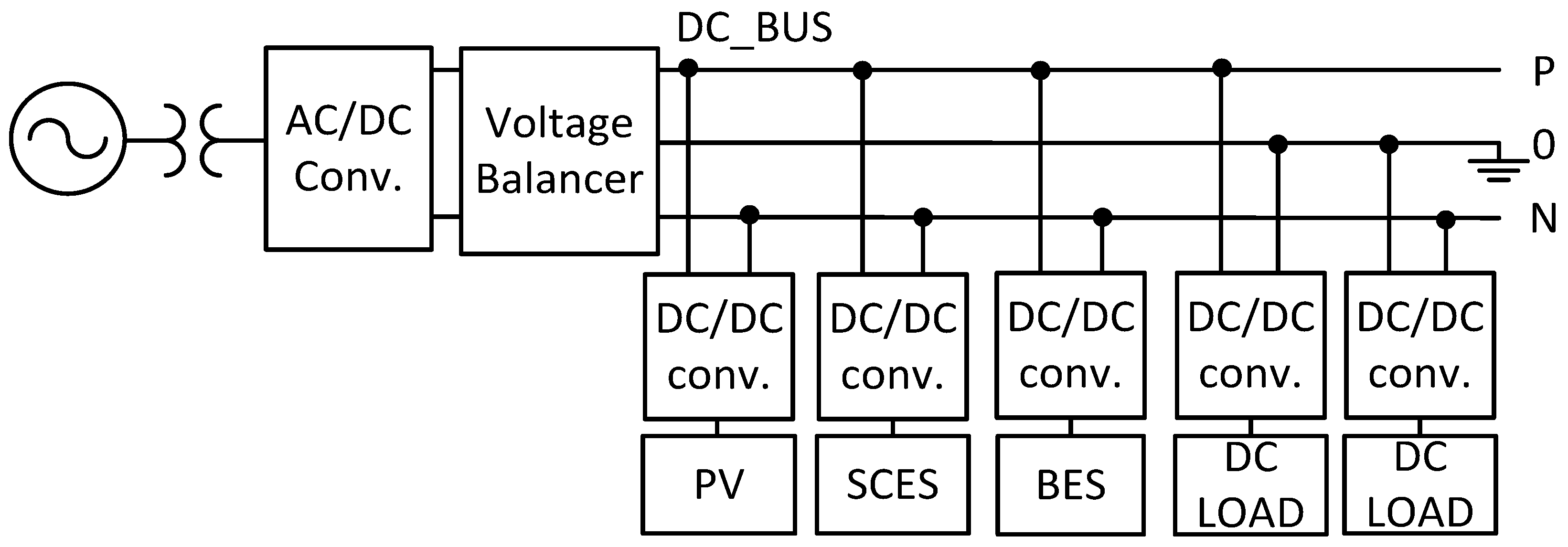
Figure 1 shows the bipolar DC distribution system configuration considered in this paper. The main DC power is supplied from the three-phase AC grid through an AC/DC converter, while the PV generator, BES (battery energy storage), and SCES (super-cap energy storage) are connected to the two bus lines, respectively. Two DC loads with different capacities are connected to the positive and negative poles, respectively. A voltage balancer is connected next to the AC-DC converter for compensating the voltage unbalance between the positive and negative poles due to the different load capacity.
Normally batteries cannot absorb the surplus power rapidly due to their slow charging process, while the super-cap can absorb transiently generated power, so a battery and super-cap are connected in parallel to operate in a hybrid form.
The controller for the bipolar DC distribution system is divided into the upper level control and the lower level control. The upper level control function is the supervision of the whole system operation which includes islanding detection and power management. Many islanding detection methods are already developed and can be applied for the bipolar DC distribution system [11,12,13]. In this paper it is assumed that islanding is detected when the system recognizes the AC grid voltage to be zero.
The power management scheme is divided into two categories, namely a grid-tied mode and an islanded mode, depending on the fault status of the AC grid. Power management algorithms for the unipolar DC micro-grid like those described in reference [2] can be applied for the bipolar DC distribution system.
2.2. Upper Level Control
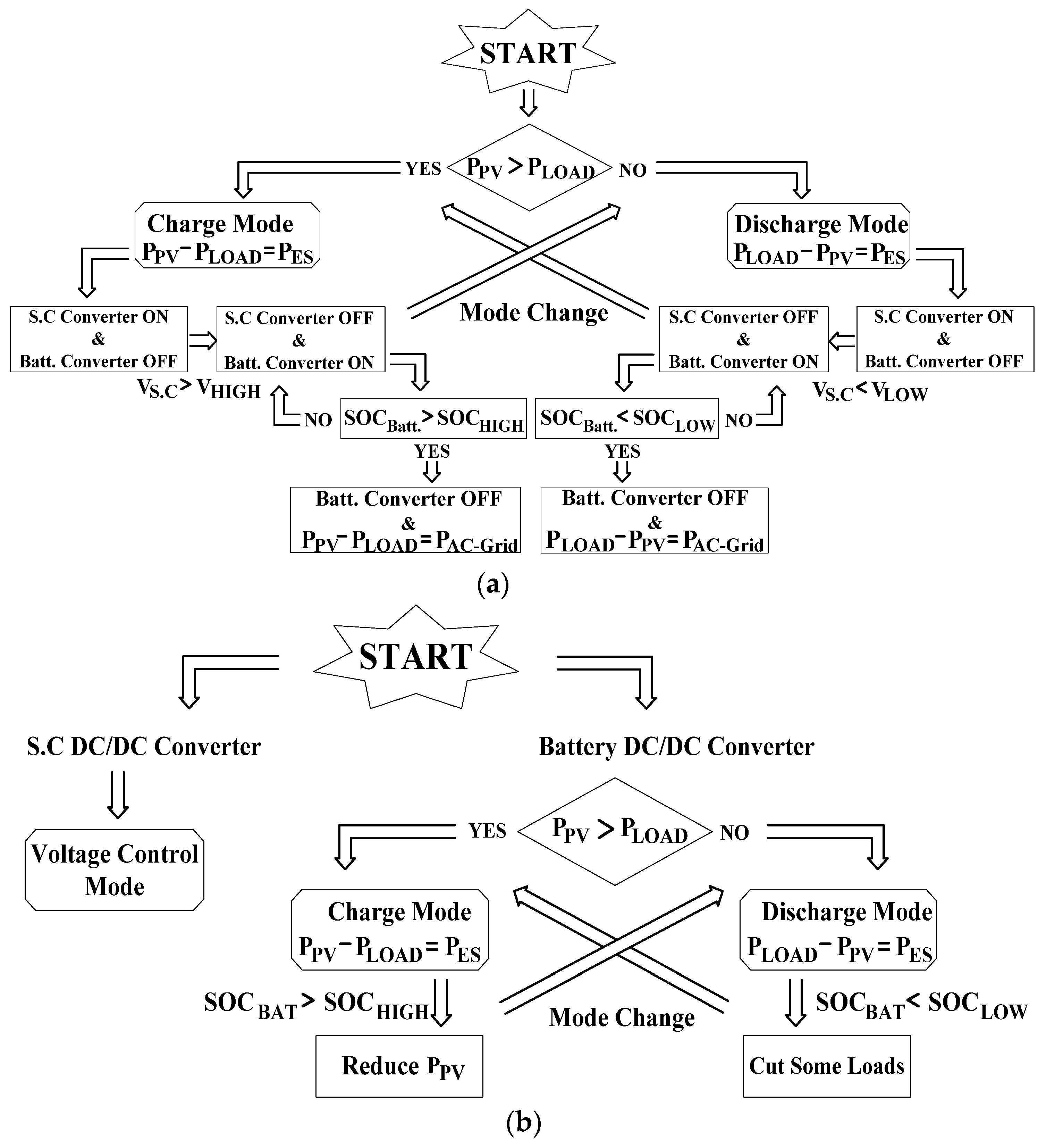
Figure 2 shows a power management logic configuration in both grid-tied mode and islanded mode. Figure 2a shows a battery energy storage operation scheme in grid-tied mode. In this mode, the grid-tied converter operates to maintain the DC grid voltage. The power produced by the photovoltaic system is measured and if this value is larger than the power consumed in the load, the difference is charged into the energy storage first. After then, if the energy storage is fully charged, the power is supplied to the associated AC power network. If the power produced by the PV generator is smaller than the power consumed in the load, the difference is taken from the power stored in the energy storage first. After that, if the energy storage is in a fully discharged mode, the required power is taken from the AC power network.
Figure 2b shows an battery energy storage operation scheme in islanded mode. In this mode the super-cap converter operates to maintain the DC grid voltage. The power produced by the PV generator is measured and if this value is larger than the power consumed in the load, the difference is charged into the energy storage first. After that, if the energy storage is in a fully charged mode, the surplus power should be removed. If the power produced by the PV generator is smaller than the power consumed in the load, the difference is taken from the power stored in the energy storage first. After then, if the energy storage is fully discharged, load sharing is carried out.
2.3. Lower Level Control
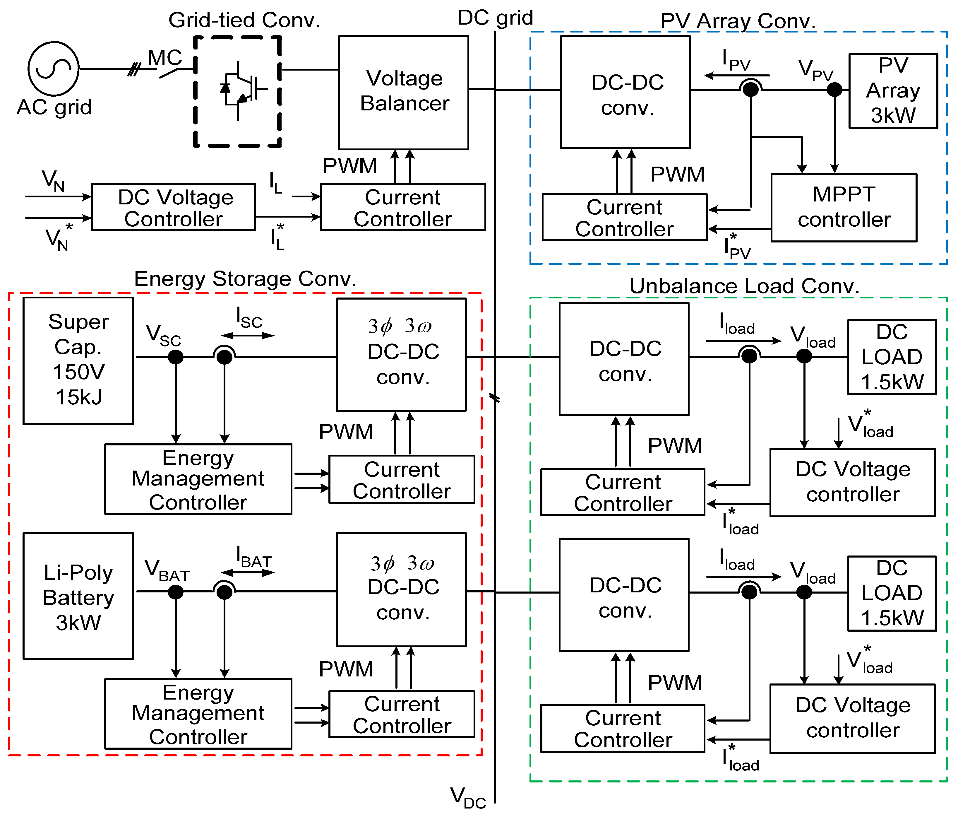
The low level control function is to maintain the DC grid voltage constant and to regulate all the DC power from the sources, energy storages, and loads by controlling the converters. Figure 3 shows a schematic diagram for the converter control in the bipolar DC distribution system considered in this paper.
In grid-tied mode, the grid-tied converter maintains the DC grid voltage through voltage control while other DC-DC converters control their output power through current control. In islanded mode, the grid-tied converter is disconnected and the DC-DC converter in battery storage or super-capacitor operates in voltage control mode to maintain the DC grid voltage. Other DC-DC converters operate in current control mode to regulate the output power.
The AC/DC converter controls the DC grid voltage by absorbing power from or delivering power to the AC grid when it operates in grid-tied mode. It separates the DC grid from the AC grid by removing the gate pulses when a fault occurs in the AC grid. The reference voltage is applied to the voltage controller to maintain the DC grid voltage constant, and the reference current generated here is compared with the actual current of the system via the current controller thereby generating 3-phase PWM gate pulse [14,15].
The DC-DC converter for the PV generator boosts the output voltage of solar array, which changes according to solar radiation and temperature, up to the DC grid voltage. This converter performs the maximum power point tracking (MPPT) control to generate the maximum power from the given solar radiation and temperature. In this paper, perturbation and observation (P&O) scheme was applied.
An interleaved three-phase DC-DC converter was used for the battery and super-cap storages, which operates in bidirectional mode for charging or discharging. This converter can reduce the ripple currents flowing into the battery and super-cap by combining three 120° phase-shifted waveforms [16,17,18,19].
The DC-DC converters for the DC loads operate in buck mode to regulate the output voltage across the resistive load for simulating the variable power consumed in the load. The unbalanced loads connected to the positive and the negative poles can be simulated by operating the DC-DC converter with different duty ratios.
2.4. Dual-Buck Voltage Balancer
Figure 4 shows the power circuit of the dual-buck voltage balancer and its controller proposed in [10], including two unbalanced resistive loads. It consists of two IGBT switches, two diodes, two inductors, and two capacitors. When the load resistor is larger than the load resistor, the switch operates in ON/OFF mode while the switch is continuously OFF. When the load resistor is smaller than the load resistor , the switch operates in ON/OFF mode while the switch is continuously OFF.
The controller measures the positive and negative pole voltages, and . Their sum is divided by 2 to obtain the reference voltage to be compared with . The difference is passed through the voltage regulator to generate the reference signal. The reference signal and its reversed signal are compared with the triangular carrier to generate the gate pulses for the switches and . The main disadvantage of a dual-buck voltage balancer is the requirement for a greater number of components which represents a cost and reliability burden. Also, the control accuracy is rather low because the controller only has one voltage regulator.
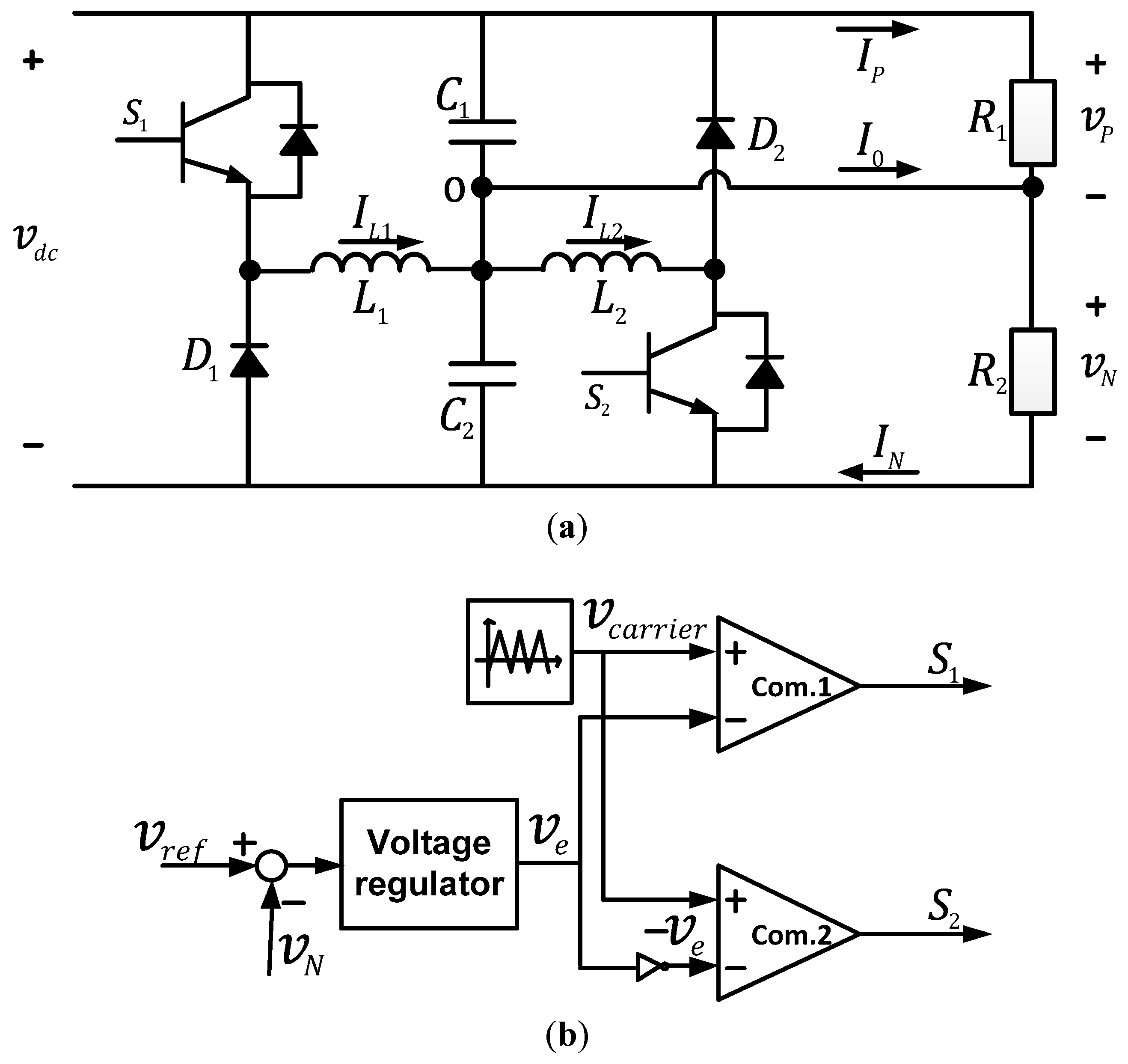
3. Half-Bridge Voltage Balancer
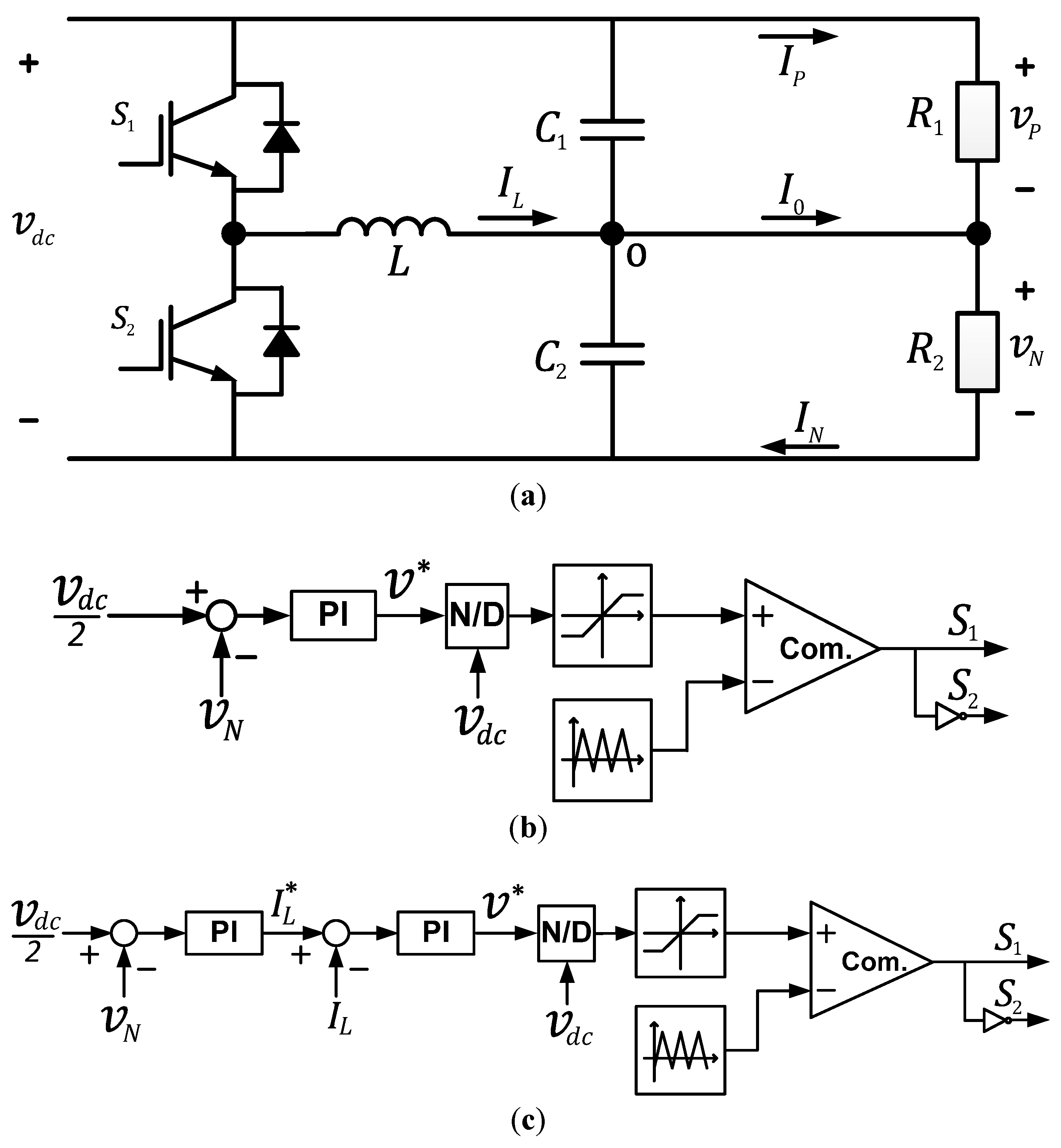
Figure 5 shows the power circuit of the half-bridge voltage balancer and its two controllers analyzed in this paper [7,9,20]. When the load resistor is larger than the load resistor , the switch operates in ON/OFF mode and the switch is continuously OFF. When the load resistor is smaller than the load resistor , the switch operates in ON/OFF mode and the switch is continuously OFF.
Figure 5b shows a voltage controller with one PI control which measures the positive and negative pole voltages, and . It calculates the that is equal to . Then this value is compared with the . The difference is passed through PI control to generate the reference voltage . Dividing the by , a reference signal for the PWM switching is obtained. PWM pulses with variable duty ratio are generated by comparing this reference signal with a triangular carrier signal.
Figure 5c shows the voltage controller proposed in this paper which consists of two cascaded PI controls. The proposed controller has an inner control loop to regulate the inductor current which offers accurate voltage regulation for the outer control loop. Therefore, the proposed controller can offer better voltage regulation than the existing controller with one PI control. The proposed controller measures the positive and negative pole voltages, and . It calculates the that is equal to and this value is compared with the . The difference is passed through PI control to generate the reference current through the reactor. Comparing this reference current with the actual reactor current , the voltage reference can be generated by having the difference pass through the PI control. Dividing the by , a reference signal for the PWM switching is obtained. PWM pulses with variable duty ratio are generated by comparing this reference signal with a triangular carrier signal.
3.1. Half-bridge Voltage Balancer with One PI Control
When the load resistor is larger than the load resistor , the switch operates in ON/OFF mode while the switch is continuously OFF. The transfer function is represented by Equation (1):
When the load resistor is smaller than the load resistor , the switch operates in ON/OFF mode while the switch is continuously OFF. The transfer function is represented by Equation (2):
Since is equal to the , the above two transfer functions can be simply represented by the following equation:
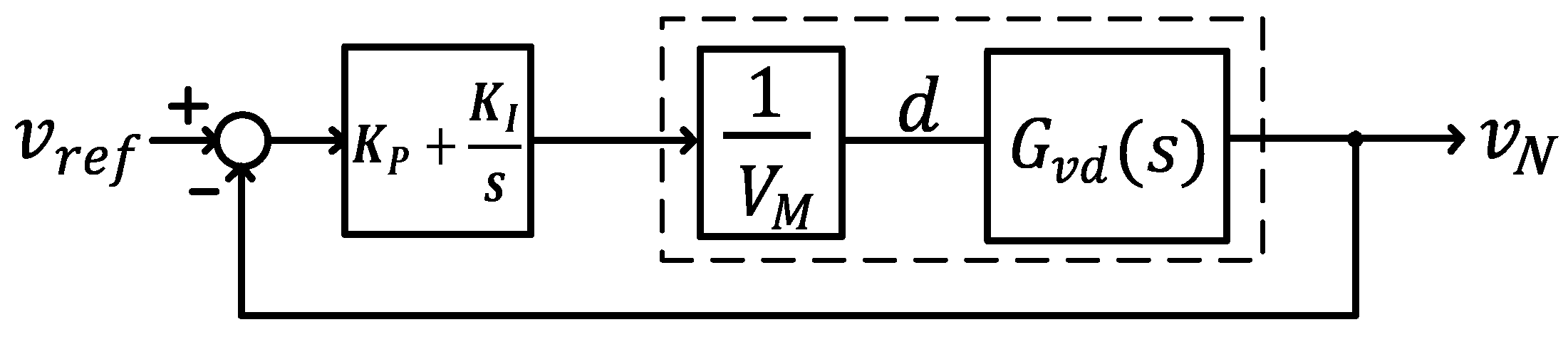
Figure 6 shows a voltage control diagram for the half-bridge voltage balancer, in which the PI control gains can be determined by setting the bandwidth of the converter model. The circuit parameters for the half-bridge voltage balancer which was used in the controller design are shown in Table 1.
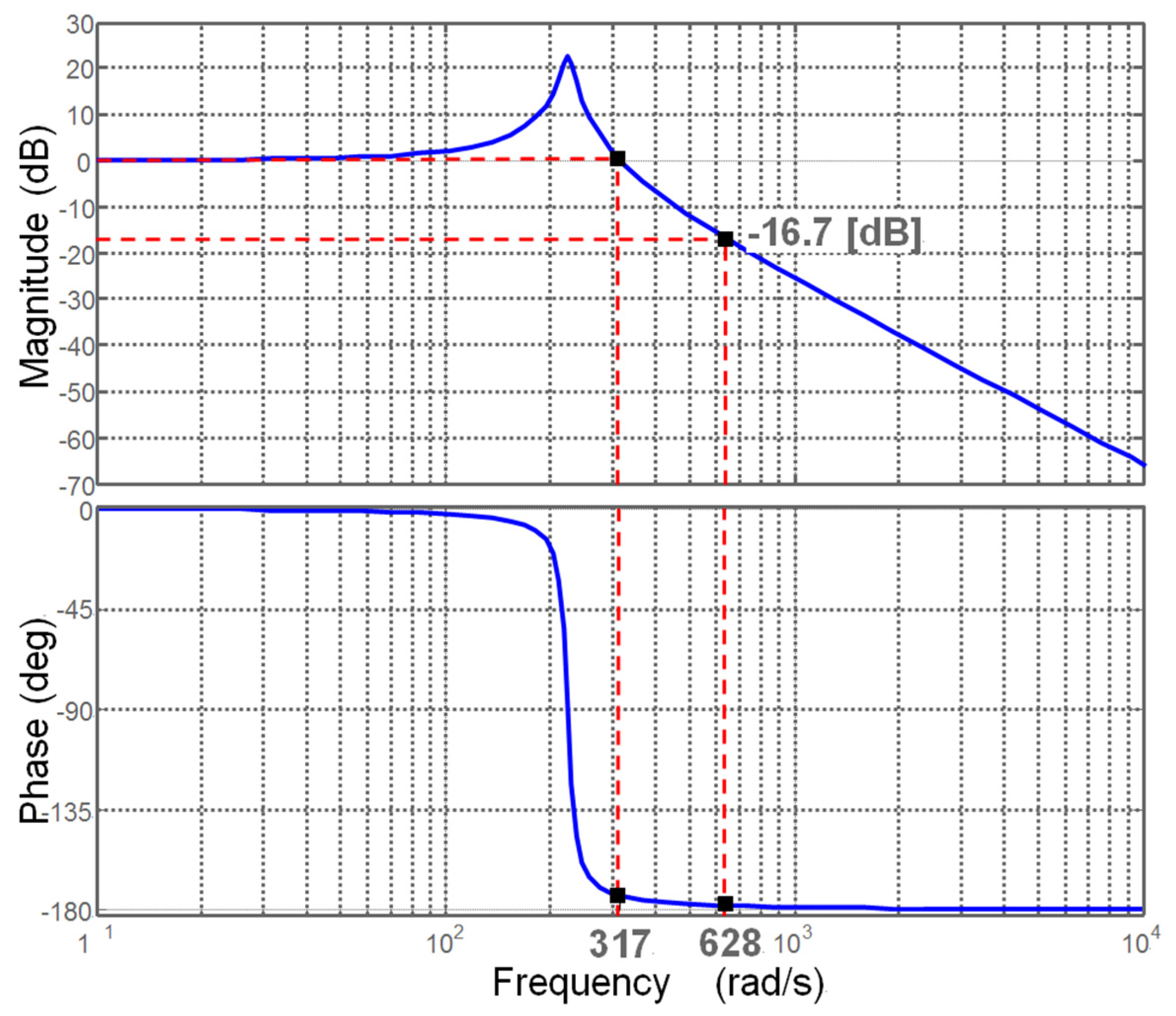
The Bode plot of the voltage control loop gain is shown in Figure 7. The bandwidth of the voltage control was set by assuming 1/100 of switching frequency, that is
Since the gain at the bandwidth of voltage control loop gain is –16.7dB, the value of proportional gain is 6.84 and the value of integral gain is 108.
According to the stability analysis result for the closed-loop voltage control, the PI control provides stable operation for the half-bridge voltage balancer with one PI control, but the stability margin is very narrow, so the half-bridge voltage balancer with the above control could be very weak for the disturbances.
3.2. Half-bridge Voltage Balancer with Two PI Control
When the load resistor is larger than the load resistor , the switch operates in ON/OFF mode. A current doesn’t flow through the switch . The transfer functions for the current control of half-bridge voltage balancer can be derived as the following two equations:
When the load resistor is smaller than the load resistor , the switch operates in ON/OFF mode. No current flows through the switch . The transfer functions for the current control and half-bridge voltage balancer can be derived as the following two equations:
The circuit parameters for the half-bridge voltage balancer are the same as those shown in Table 1. Since the is equal to , the above two sets of two transfer functions can be simplified by the following two equations:
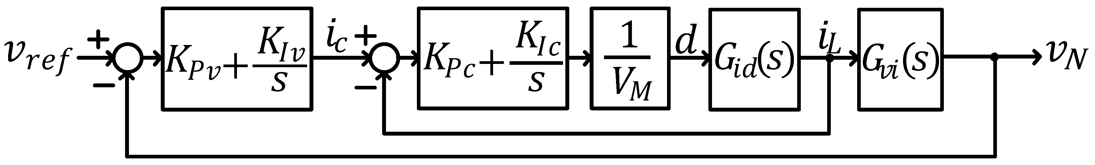
Figure 8 shows a voltage balance controller in which the gains of two PI controls can be determined by setting the converter bandwidth.
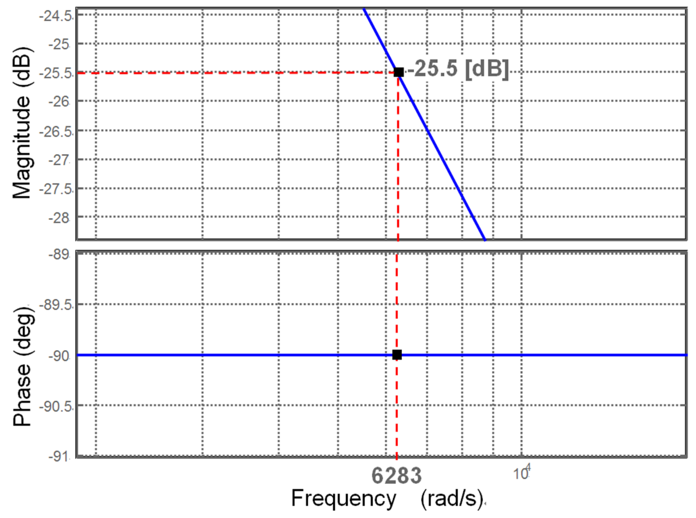
ThenBode plot for the current loop gain is shown in Figure 9. The current control bandwidth was set by assuming 1/10 of switching frequency, that is
Since the gain value at the bandwidth of the current loop gain is –25.5 dB, the value of proportional gain is 18.84 and the value of integral gain is 627.
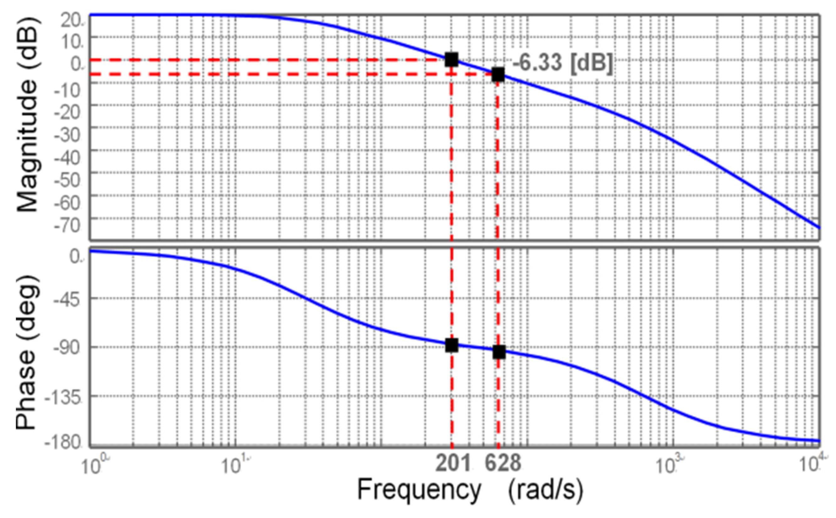
The Bode plot for the voltage loop gain is shown in Figure 10, in which is the closed loop current control transfer function. The voltage control bandwidth was set by assuming 1/10 of the current cut-off frequency, that is
3.3. Balancing Performance Analysis
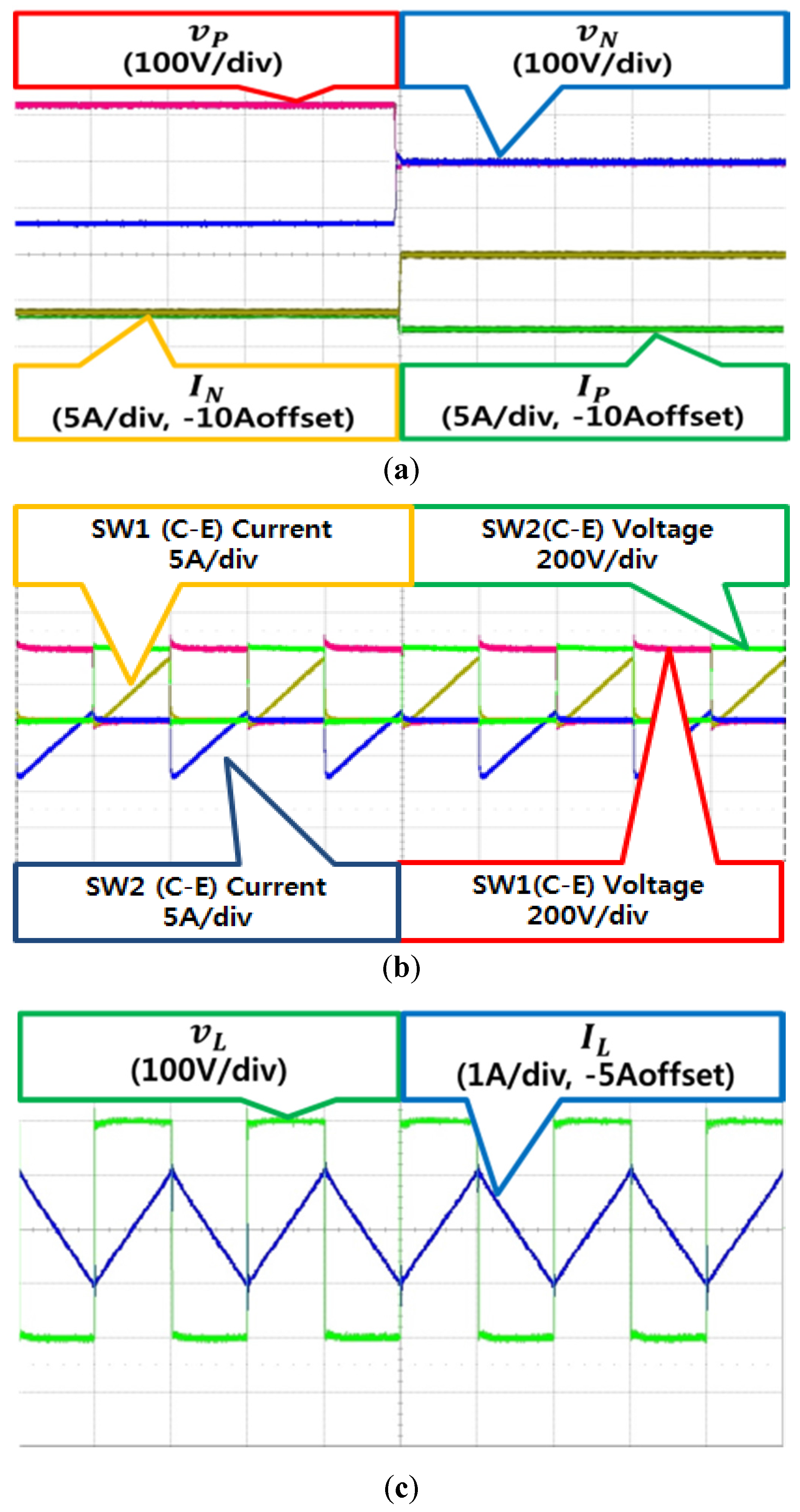
Figure 11a shows the experimental results of the half-bridge voltage balancer with the proposed controller. Before the voltage balancer is operated, the voltage at the positive terminal is 200 V and the voltage at the negative terminal is 100 V due to the difference of load resistances. On the other hand, after the voltage balancer is operated, the voltages at both terminals are the same and the load currents are different.
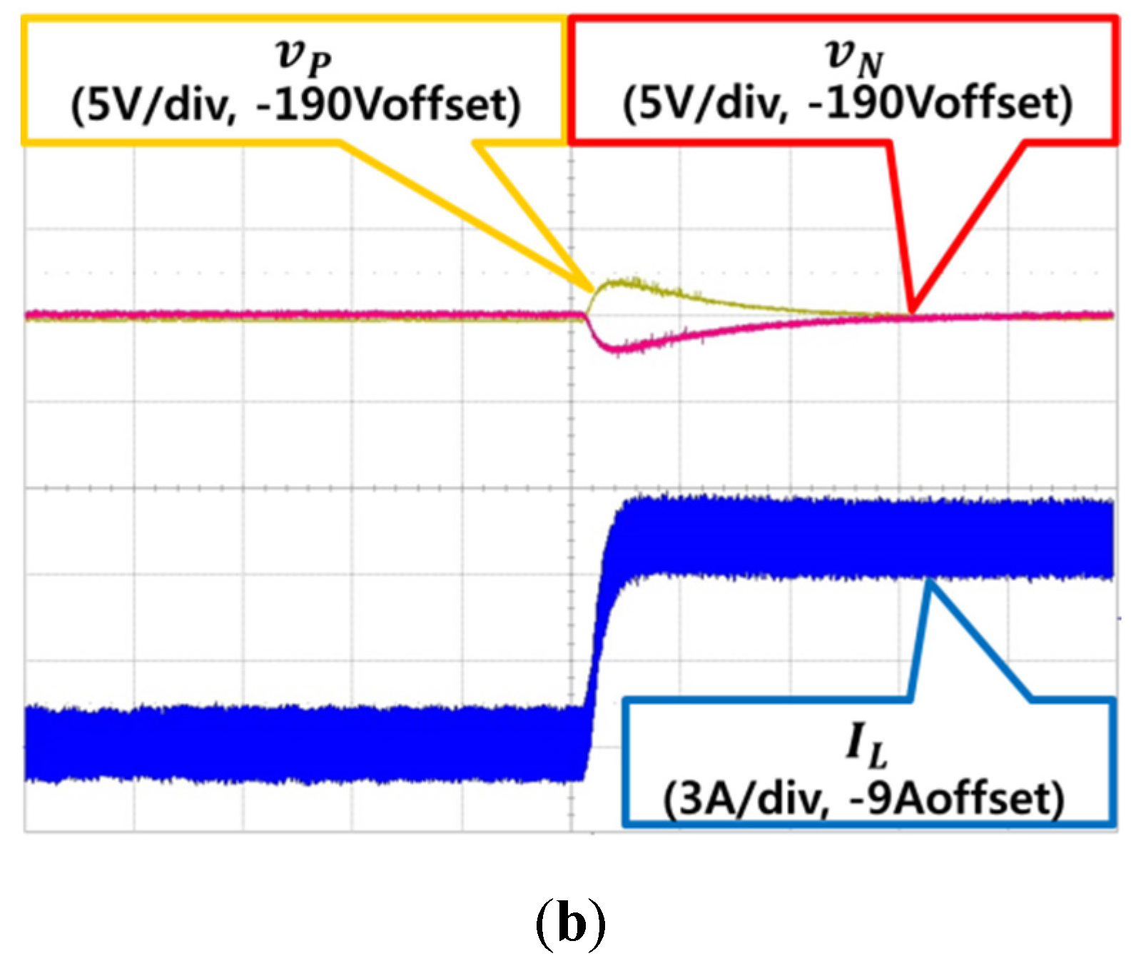
Figure 11b shows the voltage and current in the two IGBT switches. It is confirmed that zero voltage switching can be achieved by checking the waveforms of voltage and current, which offers high efficiency. Figure 11c shows the voltage and current in the inductor.
Figure 12 shows the experimental results for the half-bridge voltage balancer with one PI control and the half-bridge voltage balancer with two cascaded PI controls. The dual-buck voltage balancer with one PI control showed a voltage balancing error of 4 V, whereas the half-bridge voltage balancer with two cascaded PI controls showed a voltage balance error of nearly 0 V. This indicates that the proposed controller shows relatively more accurate voltage balancing performance.
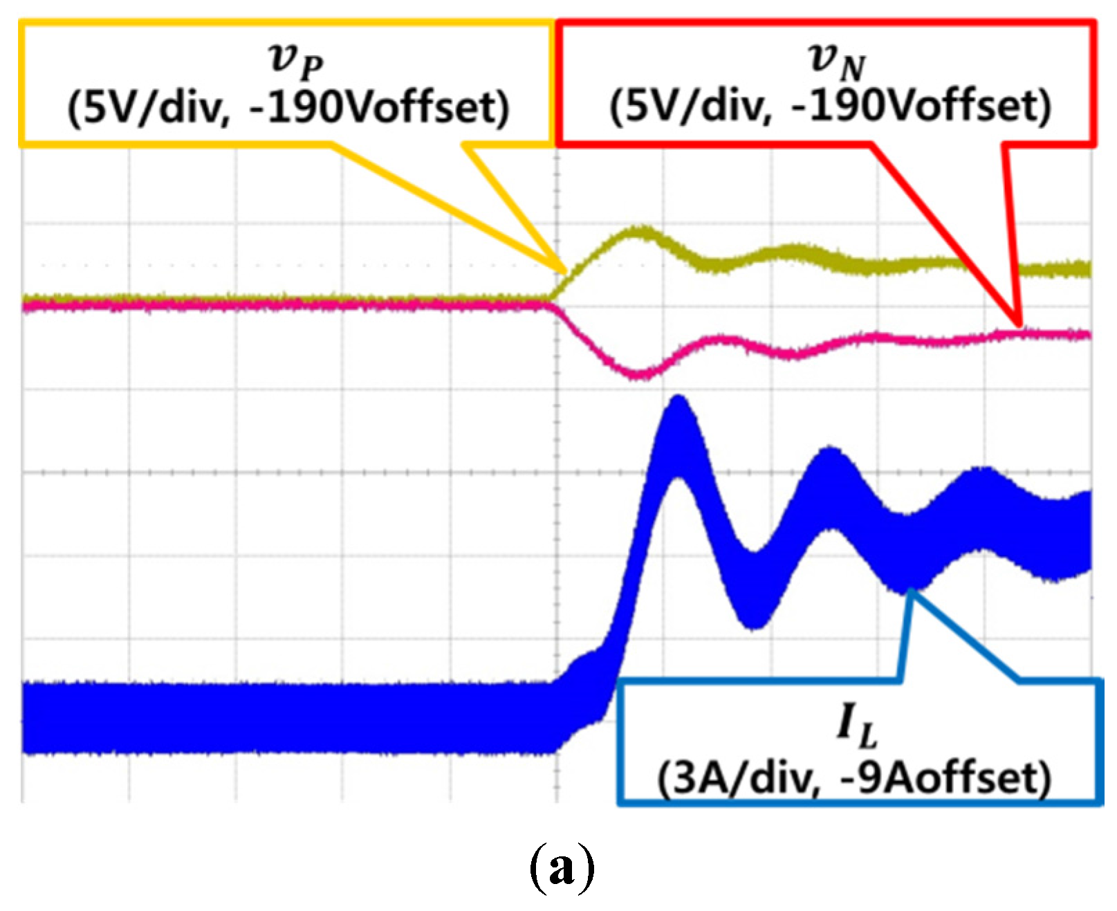
Figure 13 shows the experimental results when the load of upper pole is changed. When it is changed from 20 Ω to 100 Ω, the dual-buck voltage balancer with one PI control brings about an oscillation of the inductor current at transient state.
Also, the overshoot voltage of the upper pole is nearly 5 V and the settling time is nearly 60 ms. On the contrary, the half-bridge voltage balancer with proposed two cascaded PI controls does not cause an oscillation of the inductor current at transient state. Also, the overshoot voltage of the upper pole is nearly 1 V and the settling time is faster than that of the former voltage balancer.
4. Simulation Results and Analysis
Computer simulations were conducted to analyze the operational performance of the bipolar DC distribution system with the proposed half-bridge voltage balancer. The simulation models for photovoltaic array and battery were developed considering the operational characteristics.
The switching frequency of the PWM converter used in photovoltaic generation, battery storage, and super-cap storage was set 10 kHz. In addition, a half-bridge voltage balancer is connected right after the AC-DC converter and two loads with different capacities were connected to the positive and negative terminals in order to verify the voltage unbalance in the bipolar distribution system. The circuit parameters for the operational analysis are shown in Table 2.
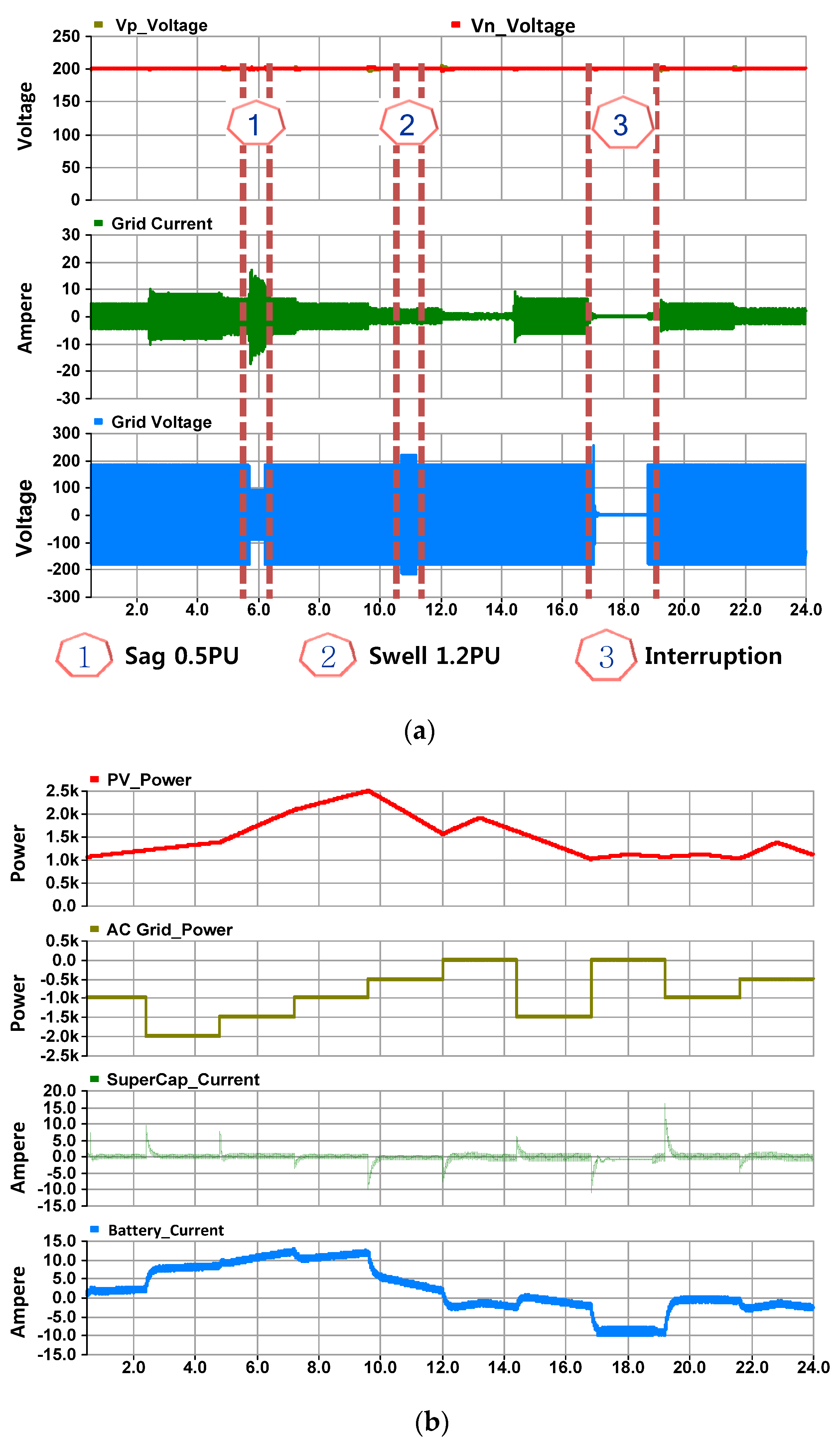
Table 3 shows the simulation scenario that was assumed to analyze the operation of the bipolar DC distribution system. First, the simulation was set to run 10 s and power consumption in the associated AC system was assumed to change in a stepwise manner. In addition, Load 1 and Load 2 were connected to the positive and negative terminals, respectively, via a chopper and a 15 Ω resistive load. The variable load was simulated by adjusting the duty ratio of the chopper so that the consumed power in the resistance changes continuously.
As shown in Figure 14, AC voltage maintains 1.0 pu for 0–1 s while absorbing power of 1.0 kW through the grid-tied converter thereby determining current introduced from the AC system accordingly. Then, 2.0 kW power is absorbed through the grid-tied converter for 1–2 s, indicating increased current introduced from AC system. For 2–3 s, AC voltage is dropped from 1.0 pu to 0.5 pu for 0.2 s followed by being recovered again to 1.0 pu. 1.5 kW power is absorbed through the grid-tied converter thereby increasing current introduced from AC system and returning back to the original value.
Then, 1 kW power is absorbed through the grid-tied converter for 3–4 s, indicating constant current introduced from the AC system. For 4–5 s, AC voltage is raised from 1.0 pu to 1.2 pu for 0.2 s, followed by being recovered again to 1.0 pu. 0.5 kW power is absorbed through the grid-tied converter thereby decreasing the current introduced from the AC system slightly and increasing again. For 5–6 s, AC voltage maintains 1.0 pu while absorbing 0.2 kW power through the grid-tied converter, indicating decreased current introduced from AC system accordingly.
For 6–7 s, AC voltage maintains 1.0 pu while absorbing 1.0 kW power through the grid-tied converter, indicating increased current introduced from AC system accordingly. For 7–8 s, AC voltage operates at 1.0 pu followed by maintaining AC voltage at 0 pu for 0.4 s and being recovered back to 1.0 pu again. When system voltage is 0, super-cap maintains DC voltage while operating solely thereby maintaining power balance of photovoltaic power generation, battery storage, and loads. For 8–10 s, AC voltage maintains 1.0 pu while absorbing 1.0 kW and 0.5 kW power through the grid-tied converter. Respectively. thereby determining current introduced from AC system accordingly. Finally, it is revealed that VP and VN were maintained at a constant value due to the voltage balancer for total operation time 10 s. Thus, a bipolar DC distribution system equipped with a voltage balancer proposed in this paper could operate stably, maintaining the DC voltage constant in grid-tied operation and islanded operation over a total operation range. Furthermore, charging or discharging current of the super-cap was run only when power was abruptly changed thereby playing a role in battery and energy storage well at the same time.
5. Hardware Experiment and Analysis
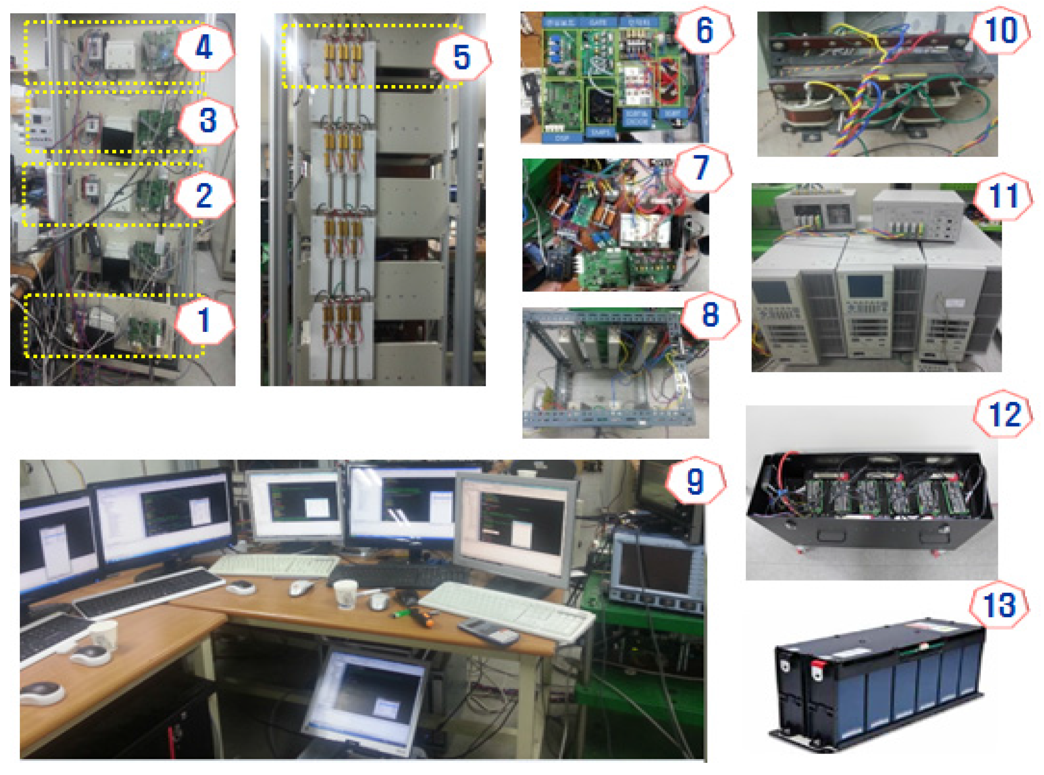
Based on the analysis result of the bipolar DC distribution system with computer simulations, an experimental set-up for the bipolar DC distribution system was manufactured and various experiments were conducted to analyze the operational characteristics in terms of hardware. Figure 15 shows a configuration of the manufactured test set-up while Table 4 shows the description of each component. A PWM converter, photovoltaic DC-DC converter, battery storage converter, and super-cap storage converter for AC system connection were manufactured as a drawer form and installed in a cabinet. A DSP controller was attached to the front side in the cabinet for control and monitoring of the converter modules and connected to the central control unit via CAN communication for power management.
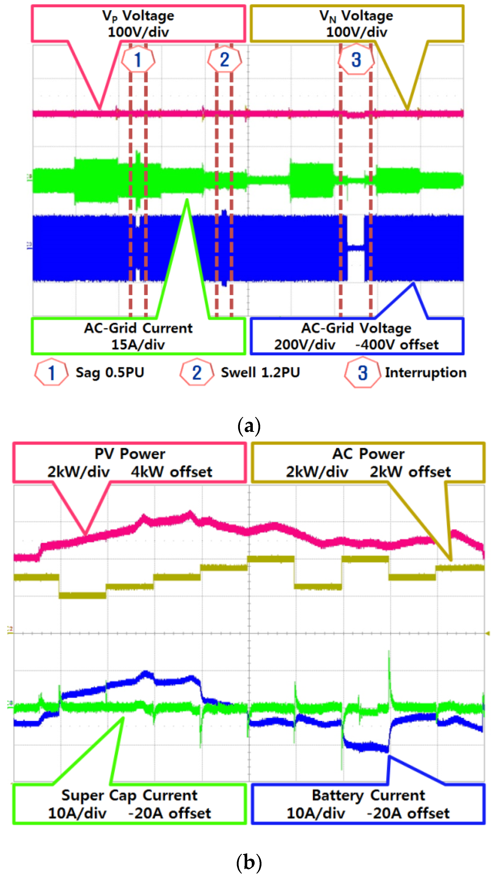
The circuit parameters related to the experimental set-up were set to the same values used in the simulation shown in Table 2. The scenario used in the experiment was also the same as the simulation, except that the operation time of experiment was set to 10 times longer than that of simulation to perform the measurement with interval of 10 s.
As shown in Figure 16, the AC voltage rwmains at 1.0 pu for 0–10 s while absorbing power of 1.0 kW through the grid-tied converter, thereby determining the current introduced from the AC system accordingly. Then, 2.0 kW power is absorbed through the grid-tied converter for 10–20 s, indicating increased current introduced from the AC system. For 20–30 s, the AC voltage is dropped from 1.0 pu to 0.5 pu for 2 s, followed by being recovered again to 1.0 pu. 1.5 kW power is absorbed through the grid-tied converter thereby increasing the current introduced from the AC system and returning back to the original value. Then, 1.0 kW power is absorbed through the grid-tied converter for 30–40 s, indicating constant current introduced from the AC system. For 40–50 s, the AC voltage is raised from 1.0 pu to 1.2 pu for 2 s, followed by being recovered again to 1.0 pu. 0.5 kW power is absorbed through the grid-tied converter thereby decreasing the current introduced from the AC system slightly and increasing again.
For 50–60 s, the AC voltage remains at 1.0 pu while absorbing 0.2 kW power through the grid-tied converter, indicating decreased current introduced from AC system accordingly. For 60–70 s, the AC voltage remains at 1.0 pu while absorbing 1.0 kW power through the grid-tied converter, indicating increased current introduced from AC system accordingly. For 70–80 s, the AC voltage operates at 1.0 pu followed by operating the associated AC voltage at 0 pu for 4 s and recovering back to 1.0 pu again. When the AC voltage is 0, the super-cap maintains the DC voltage thereby maintaining the power balance of photovoltaic power generation, battery storage, and loads. For 80–100 s, the AC voltage remains at 1.0 pu while absorbing 1.0 kW and 0.5 kW power through the grid-tied converter, respectively. thereby determining current introduced from the AC system accordingly.
Finally, it is revealed that VP and VN were maintained at a constant value due to the voltage balancer for total operation time of 100 s. Thus, a bipolar DC distribution system equipped with a voltage balancer could operate stably, maintaining the DC voltage constant in grid-tied operation and islanded operation over a total operation range. The abovementioned experimental result had the same result as the previous simulation result, except for operating 10 times slower. Furthermore, charging or discharging current of the super-cap was run only when power was abruptly changed thereby playing a key role in battery and energy storage at the same time.
6. Conclusions
This paper proposes a half-bridge voltage balancer with a new controller for a bipolar DC distribution system. The newly developed controller consists of two cascaded Proportional Integral (PI) controls for current and voltage regulation.
The performance of the newly developed controller was compared with the existing control using an equivalent circuit for the bipolar DC distribution system. The excellence of the proposed controller was verified for a typical bipolar DC distribution system through computer simulations and experiments with a scaled prototype that was manufactured in the lab.
The dynamic operation under the AC voltage sag and swell was also analyzed in detail by computer simulations and experiments with the hardware prototype. Also, the dynamic operation change from the grid-tied mode to the islanded mode and vice versa was analyzed by computer simulations and experiments. It is confirmed that the experimental results are almost similar to the simulation results.
Acknowledgments
This work was supported by human resources development propgram (#20134030200310) of KETEP grant funded by Korea Ministry of Trade, Indusrtry, and Energy. Also this work was supported by the MOF grant (Development of the design technologies for a 10MW class wave and offshore wind hybrid power generation system and establishment of the sea test infra-structure).
Conflicts of Interest
The author declares no conflict of interest.
References
- Ito, Y.; Zhongqing, Y.; Akagi, H. DC Micro-grid Based Distribution Power Generation System. In Proceedings of the 4th IEEE International Power Electronics and Motion Control Conference, Xi’an, China, 14–16 August 2004; pp. 1740–1745.
- Lee, H.J.; Kim, H.J.; Han, B.M. Operation analysis of a Communication-Based DC Micro-Grid Using a Hardware Simulator. J. Power Electron. 2013, 13, 313–321. [Google Scholar] [CrossRef]
- Kakigano, H.; Miura, Y.; Ise, T.; Uchida, R. DC Micro-grid for Super High-Quality Distribution-System Configuration and Control of Distributed Generation and Energy Storage Devices. In Proceedings of the 37th IEEE Power Electronics Specialists Conference (PESC ’06), Jeju, Korea, 18–22 June 2006.
- Kaipia, T.; Nuutinen, P.; Pinomaa, A.; Lana, A.; Partanen, J.; Lohjala, J.; Matikainen, M. Field test environment for LVDC distribution–Implementation experiences. In Proceedings of the Integration of Renewables into the Distribution Grid (CIRED) Workshop, Lisbon, Portugal, 29–30 May 2012; pp. 1–4.
- Gu, Y.J.; Chi, Y.N.; Li, Y.; Sun, W.; Li, W.H.; He, X.N. DC symmetrical component method for analysis and control of bipolar LVDC grid. In Proceedings of the IEEE Applied Power Electronics Conference and Exposition (APEC), Charlotte, NC, USA, 15–19 March 2015; pp. 2802–2807.
- Salonen, P.; Nuutinen, P.; Peltoniemi, P.; Partanen, J. LVDC distribution system protection—Solutions, implementation and measurements. In Proceedings of the 13th IEEE European Power Electronics and Applications Conference (EPE '09), Barcelona, Spain, 8–10 September 2009; pp. 1–10.
- Kakigano, H.; Miura, Y.; Ise, T.; Uchida, R. DC Voltage Control of the DC Micro grid for Super High Quality Distribution. In Proceedings of the IEEE Power Conversion Conference (PCC '07), Nagoya, Japan, 2–5 April 2007; pp. 518–525.
- Lago, J.; Moia, J.; Heldwein, M.L. Evaluation of Power Converter to Implement Bipolar DC Active Distribution Networks—DC-DC Converters. In Proceedings of the IEEE Energy Conversion Congress and Exposition (ECCE), Phoenix, AZ, USA, 17–22 September 2011; pp. 985–990.
- Kakigano, H.; Miura, Y.; Ise, T. Low-Voltage Bipolar-Type DC Microgrid for Super High Quality Distribution. IEEE Trans on Power Electron. 2010, 25, 3066–3075. [Google Scholar] [CrossRef]
- Zhang, X.J.; Gong, C.Y. Dual-Buck Half-Bridge Voltage Balancer. IEEE Trans. Ind. Electron. 2013, 60, 3157–3164. [Google Scholar] [CrossRef]
- Byeon, G.; Kim, S.K.; Kim, J.Y.; Jeon, J.H.; Kim, G.H. Cooperative ESS management strategy for stable islanded operations in a bipolar-type LVDC system. In Proceedings of the IEEE Smart Electric Distribution Systems and Technologies (EDST) International Symposium, Vienna, Austria, 8–11 September 2015; pp. 290–295.
- Karimi, H.; Yazdani, A.; Iravani, R. Negative-Sequence Current Injection for Fast Islanding Detection of a Distributed Resources. IEEE Trans. Power Electron. 2008, 23, 298–307. [Google Scholar] [CrossRef]
- Lopes, L.A.C.; Sun, H. Performance assessment of active frequency drifting islanding detection methods. IEEE Trans. Energy Convers 2006, 21, 171–180. [Google Scholar] [CrossRef]
- Moia, J.; Lago, J.; Perin, J.; Heldwein, L. Comparison of three-phase PWM rectifiers to interface AC grids and bipolar DC active distribution networks. In Proceedings of the 3rd IEEE International Symposium on Power Electronics for Distributed Generation Systems (PEDG), Aalborg, Denmark, 25–28 June 2012; pp. 221–228.
- Moia, J.; Lobo Heldwein, M. Three-level NPC-based bidirectional PWM converter operation for high availability/power quality bipolar DC distribution networks. In Proceedings of the 15th European Conference on Power Electronics and Applications (EPE), Lille, France, 2–6 September 2013; pp. 1–10.
- Liu, B.Q.; Zhuo, F.; Bao, X.W. Control method of the transient compensation process of a hybrid energy storage system based on battery and Ultra-capacitor in Micro-Grid. In Proceedings of the IEEE International Symposium on Industrial Electronics (ISIE), Hangzhou, China, 28–31 May 2012; pp. 1325–1329.
- Tremblay, O.; Dessaint, L.A.; Dekkiche, A.I. A Generic Battery Model for the Dynamic Simulation of Hybrid Electric Vehicles. In Proceedings of the IEEE Vehicle Power and Propulsion Conference (VPPC), Arlington, TX, USA, 9–12 September 2007; pp. 284–289.
- Lee, W.; Han, B.M.; Cha, H. Battery ripple current reduction in a three-phase interleaved dc-dc converter for 5kW battery charger. In Proceedings of the IEEE Energy Conversion Congress and Exposition (ECCE), Phoenix, AZ, USA, 17–22 September 2011; pp. 3535–3540.
- Soeiro, T.B.; Heldwein, M. Bidirectional three-phase buck-+boost-type PFC rectifier for bipolar DC distribution systems. In Proceedings of the 15th European Conference Power Electronics and Applications (EPE), Lille, France, 2–6 September 2013; pp. 1–10.
- Kakigano, H.; Miura, Y.; Ise, T. Distribution Voltage Control for DC Microgrids Using Fuzzy Control and Gain-Scheduling Technique. IEEE Trans on Power Electron. 2013, 28, 2246–2258. [Google Scholar] [CrossRef]
Figure 1.
Bipolar DC distribution system.

Figure 2.
Power management logic: (a) Grid-tied mode; (b) Islanded mode.

Figure 3.
Power converter controller.

Figure 4.
Dual-buck voltage balancer: (a) Power circuit; (b) Controller.

Figure 5.
Half-Bridge voltage balancer: (a) Power circuit; (b) Controller with one PI control; (c) Controller with two cascaded PI controls.
Figure 5.
Half-Bridge voltage balancer: (a) Power circuit; (b) Controller with one PI control; (c) Controller with two cascaded PI controls.

Figure 6.
Control block for voltage control.

Figure 7.
Bode plot for voltage control loop gain

Figure 8.
Control block for current and voltage control.

Figure 9.
Bode plot for current control.

Figure 10.
Bode plot for voltage control.

Figure 11.
Experimental results of half-bridge voltage balancer with proposed controller: (a) Load voltage and current; (b) Switch voltage and current; (c) Inductor voltage and current.
Figure 11.
Experimental results of half-bridge voltage balancer with proposed controller: (a) Load voltage and current; (b) Switch voltage and current; (c) Inductor voltage and current.

Figure 12.
Performance comparison in voltage balancing: (a) One PI voltage control; (b) Two cascaded PI controls.
Figure 12.
Performance comparison in voltage balancing: (a) One PI voltage control; (b) Two cascaded PI controls.

Figure 13.
Performance comparison in voltage balancing: (a) One PI voltage control; (b) Two cascaded PI controls.
Figure 13.
Performance comparison in voltage balancing: (a) One PI voltage control; (b) Two cascaded PI controls.


Figure 14.
Simulation results for operation analysis: (a) DC voltage and AC grid current & voltage; (b) PV power, bulk power, SC current, BAT current
Figure 14.
Simulation results for operation analysis: (a) DC voltage and AC grid current & voltage; (b) PV power, bulk power, SC current, BAT current

Figure 15.
Hardware experimental set-up.

Figure 16.
Experimental results for operation analysis: (a) DC voltage and AC grid current & voltage, (b) PV power, bulk power, SC current, BAT current.
Figure 16.
Experimental results for operation analysis: (a) DC voltage and AC grid current & voltage, (b) PV power, bulk power, SC current, BAT current.


| Circuit Parameters | Values |
|---|---|
| 400 V | |
| 3 mH | |
| 3300 µF | |
| 100 Ω | |
| 20 Ω |
| Grid-Tied 3-level Inverter | |||||||||
|---|---|---|---|---|---|---|---|---|---|
| Coupling Reactor | DC-Link Capacitor | ||||||||
| 3 mH | 1650 µF | ||||||||
| Coupling Transformer | |||||||||
| Turn Ratio | Rated Power | Coupling Type | Leakage Impedance | ||||||
| 220:220 | 5 kVA | Y-Y | 1.5% | ||||||
| Super Capacitor | |||||||||
| Capacitance | Max Current | Capacity | Rated Voltage | Life Cycle | |||||
| 1.67 F | 60 A | 16 kJ | 162 V | 500,000 | |||||
| Li-Polymer Battery | |||||||||
| Capacity | Rated Voltage | ||||||||
| 31 A | 260 V | ||||||||
| Photovoltaic | |||||||||
| Max Power | Max Voltage | Max Current | |||||||
| 3 kW | 250 V | 12 A | |||||||
| Unbalance DC LOAD | |||||||||
| DC Load 1 | DC Load 2 | Reactor | Capacitor | ||||||
| 15 Ω | 15 Ω | 3 mH | 1000 µF | ||||||
| Voltage Balancer Converter | |||||||||
| Balancer Reactor | DC-Link Capacitor | ||||||||
| 1 mH | 1650 µF | ||||||||
| Time | Grid_V | LOAD_1 | LOAD_2 | BULK | Op_Mode |
|---|---|---|---|---|---|
| ~1 s | 1.0 pu | 1500 W | 166 W | –1 kW | Grid-Tied |
| ~2 s | 1500 W | 0 W | –2 kW | ||
| ~3 s | 0.5 pu | 166 W | 666 W | –1.5 kW | |
| ~4 s | 1.0 pu | 666 W | 166 W | –1 kW | |
| ~5 s | 1.2 pu | 166 W | 1500 W | –0.5 kW | |
| ~6 s | 1.0 pu | 1500 W | 666 W | –0.2 kW | |
| ~7 s | 1500 W | 1500 W | –1 kW | ||
| ~8 s | 0.0 pu | 1500 W | 1500 W | 0 kW | Grid-Off |
| Item No. | Designation | Item No. | Designation |
|---|---|---|---|
| 1 | Grid-tied Converter | 8 | DC Loads |
| 2 | PV Converter | 9 | Main Controller |
| 3 | SC Converter | 10 | Transformer [1:1] |
| 4 | Battery Converter | 11 | 3-Phase AC Source |
| 5 | Line Impedance | 12 | Li-Polymer Battery |
| 6 | Voltage Balancer | 13 | Super-Cap |
| 7 | Buck Converters |
© 2016 by the author; licensee MDPI, Basel, Switzerland. This article is an open access article distributed under the terms and conditions of the Creative Commons by Attribution (CC-BY) license (http://creativecommons.org/licenses/by/4.0/).
Share and Cite
MDPI and ACS Style
Han, B.-M. A Half-Bridge Voltage Balancer with New Controller for Bipolar DC Distribution Systems. Energies 2016, 9, 182. https://doi.org/10.3390/en9030182
AMA Style
Han B-M. A Half-Bridge Voltage Balancer with New Controller for Bipolar DC Distribution Systems. Energies. 2016; 9(3):182. https://doi.org/10.3390/en9030182
Chicago/Turabian StyleHan, Byung-Moon. 2016. "A Half-Bridge Voltage Balancer with New Controller for Bipolar DC Distribution Systems" Energies 9, no. 3: 182. https://doi.org/10.3390/en9030182
Note that from the first issue of 2016, this journal uses article numbers instead of page numbers. See further details here.