1. Introduction
Energy has become one of the most important parts of our lives and, due to its widespread use and effects, there is a need to create methods of conserving it, particularly to prevent further air pollution. Many countries have invested heavily in developing electric vehicles (EVs), which usually contain three parts: a driving motor, a power transmission system, and a power supply system. The first two technologies have been heavily investigated and are becoming increasingly reliable. However, the power battery pack, which influences the driving mileage, requires further optimization before electric vehicles can be commercialized successfully. The power battery pack testing system is used to evaluate the performance of power accumulator batteries, and it plays an important role in choosing and comparing batteries for EVs. There has been considerable research on battery pack testing systems [
1,
2,
3,
4,
5,
6,
7,
8,
9,
10]. A bi-directional energy flow power circuit topology combined with the control scheme used for power accumulator battery pack testing system (PABPTS) was designed to reduce the energy required for discharge test experiments and was described in [
11]. This technology can integrate discharging energy of Li-ion battery with the power grid, and is called an energy recovery power accumulator battery pack testing system (ERPABPTS).
Most conventional ERLPABTSs featuring bi-directional two-level voltage source converters for DC-AC transformation have suffered from large switching stress and wastage. This is because conventional ERLPABTSs have the drawbacks of high total harmonic distortion, power transistors in the two-level converter when used for medium voltage (e.g., 900–1000 V), and high power output (e.g., 250 kW). Voltage rating requirements are much higher for two-level voltage source converters. The neutral-point-clamped (NPC) PWM inverter, which was first described by Nabae and Akira [
12] in 1981, has emerged as a solution for working with higher voltage levels. The commutation of the switches permits the addition of capacitor voltages, which can reach high voltages at the output, while the power semiconductors only need to withstand reduced voltages [
13]. The following attractive features could be achieved if NPC-based three-level converters could be integrated into the power circuit topology of ERPBTSs: (1) extremely low distortion and low d
v/dt of the output voltage; (2) low distortion input current draw with structure-type filters (such as LCL filters) simplified to L filters; (3) low switching frequencies that would significantly reduce switching loss; (4) smaller common-mode (CM) voltage to reduce the stress in motor bearings. In addition, the CM voltage could be eliminated by using proper methods [
14].
A great deal of work related to the multi-level converter topology, control schemes, and their applications has been done in the last ten years [
15,
16,
17]. Mondal
et al. [
18] extended the space voltage pulse width modulation (SVPWM) of the three-level inverter into the over-modulation region. Busquets-Monge
et al. [
19] presented a new modulation approach for the complete control of the neutral-point voltage in a three-level three-phase NPC voltage source inverter. The modulation approach was based on the virtual space vector concept, which guarantees the balancing of the neutral-point voltages for any load (whether linear or nonlinear) over the full range of converter output voltage and for all load power factors, with the only requirement being that the sum of the three-phase output currents is zero. Implementing the modulation was simple based on the phase duty-ratio expressions. A hybrid PWM modulation scheme [
20] that uses both SVPWM and virtual SVPWM (VSVPWM) was presented, and allowed for complete control of the neutral point voltage in NPC three-level inverters, the performance of which was verified through simulation and experiment. In addition to the advanced modulation scheme, Verveckken
et al. [
21] developed a direct power control (DPC) method based on instantaneous power theory to apply the full potential of a power converter to a grid-connected system. Another typical application of multi-level converters is in AC motor driving systems where direct torque control (DTC) of induction motors using NPC three-level converters was described in [
22,
23,
24].
The aim of this paper is to further extend sliding mode control to ERLPBTS using a three-level NPC converter. This is based on the work done in [
25,
26], but differs from previous research in that, for the first time, the inner current decoupling control method combined with sliding mode control is illustrated, along with an optimal switching table for the convergence of an equivalent input voltage for an NPC-based voltage source converter. The surface derivation and the principle of decoupling between phases are presented. Specifically, comparisons between the proposed scheme (sliding mode control) and the conventional proportional integral (PI) control scheme in the discharging current test of the PBPTS are presented. Another contribution of this paper is the elimination of the need for an isolation transformer, which makes the system more efficient as well as being lighter and smaller in volume.
This paper is arranged as follows: in
Section 2, we explain the configuration and operation principles of the ERLPBPTS when it works in discharging mode. In
Section 3, the saturation-restrained inner sliding model controlled current decoupling control scheme which is combined with an optimal switching table, are designed to integrate the three-level inverter to an AC-grid. We also design a fast dynamic time response current controller for discharging tests with minimum overshoot by establishing the dynamic equation of the small signal average model. In
Section 4, simulations are performed to demonstrate the feasibility and correctness of the recommended scheme. The hardware setup and experimental results to verify the proposed scheme are given in
Section 5. Finally, conclusions and suggested future works are presented in
Section 6.
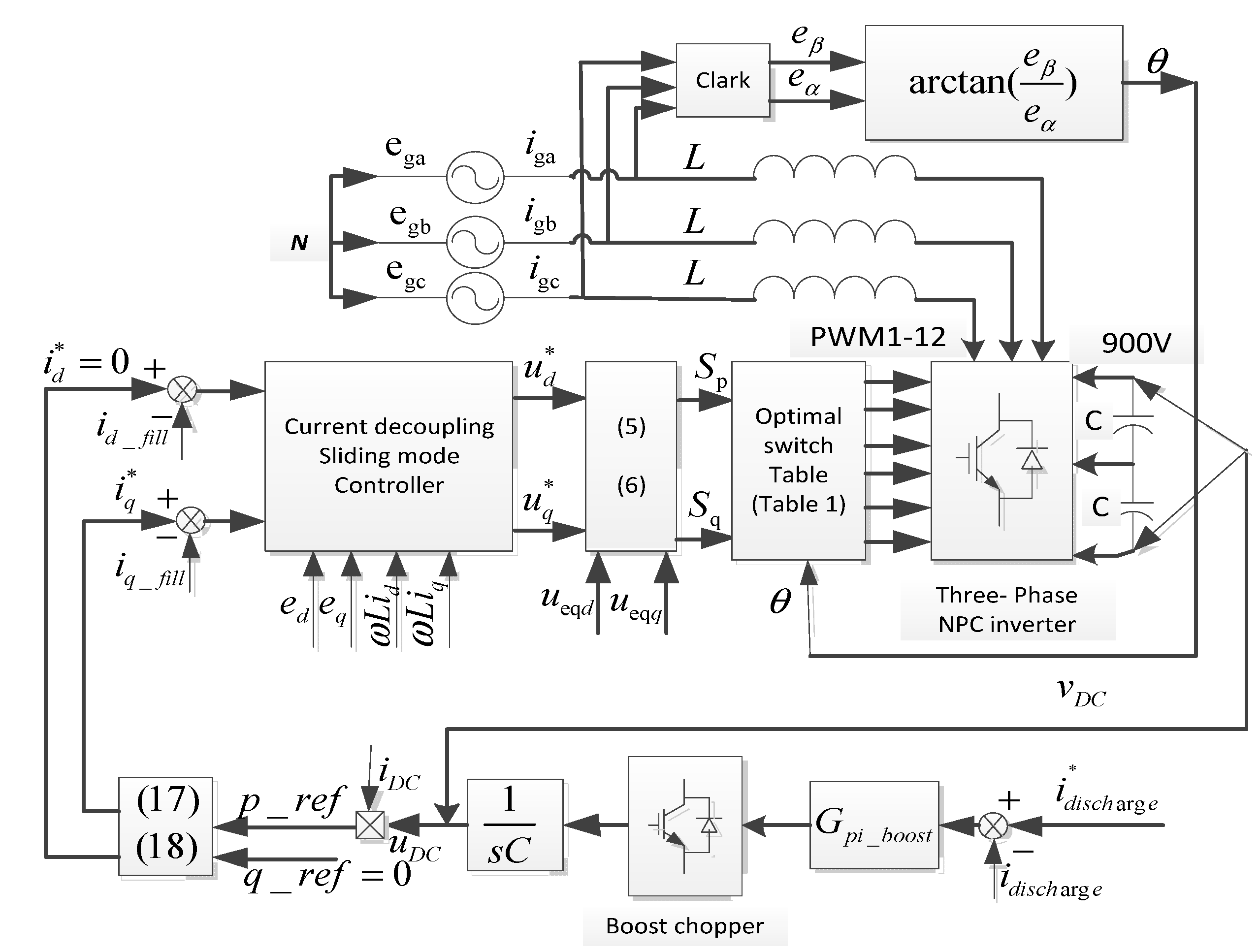
2. Configuration, Operation Principle, and Mathematical Model of NPC-Based Transformerless Three-Level ERPBPTS
2.1. Composite Power Circuit Description
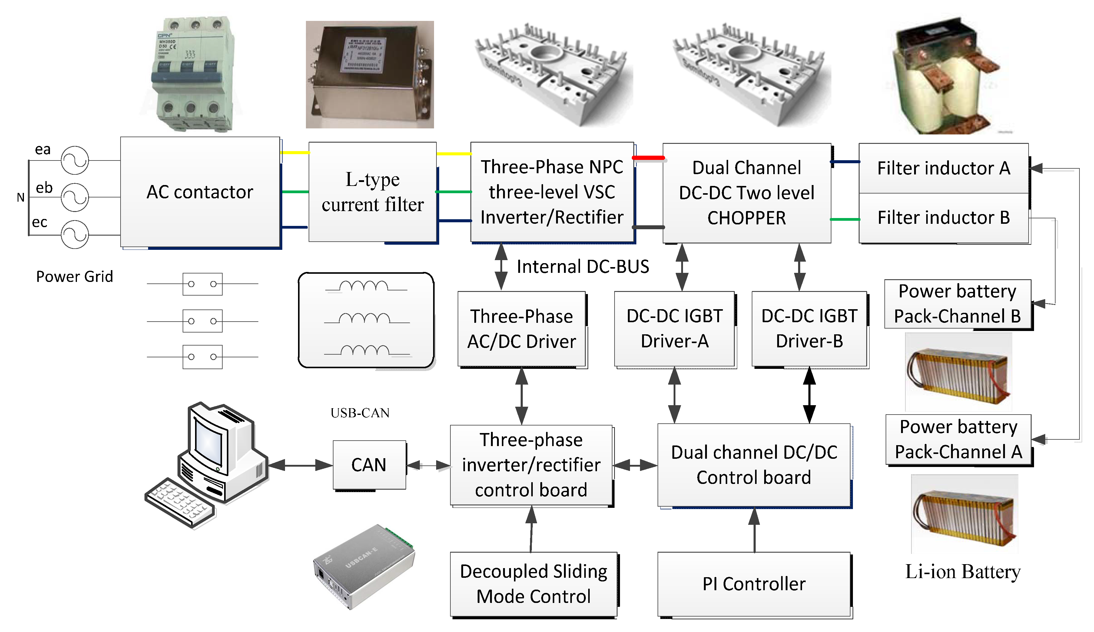
The diagram of the improved ERLPABTS is shown in
Figure 1. It is used for the two-channel ERPBPTS. Compared with conventional two-level ERLPABTS system in [
11], it is easily seen that there is no isolation transformer in the power circuit. The three-phase AC-DC rectifier/inverter and the DC-DC buck-boost chopper are composed of a three-level diode-clamped NPC-VSC converter. Hence, the configuration of the whole system contains the following parts:
- (a)
A three-phase breaker on grid-side for short circuit protection;
- (b)
Three L-type filters for higher-order current harmonic elimination;
- (c)
A three-phase, three-line, three-level NPC-VSC inverter/rectifier on the inverter side;
- (d)
A dual-channel DC-DC buck-boost chopper for charging and discharging control of the power accumulator battery pack;
- (e)
Two large value DC current filter inductors in channels A and B are used to minimize the current ripple while performing current test experiments;
- (f)
The DC-DC buck and boost chopper shares the same dc-link voltage. Large value and volume DC-bus capacitors are needed to keep the dc-link voltage constant;
- (g)
Dual channel power battery packs for load testing, which can be a lead-acid battery, lithium-ion battery, or super-capacity battery.
Figure 1.
Block diagram of the ERLPABTS using an improved NPC-VSC converter.
Figure 1.
Block diagram of the ERLPABTS using an improved NPC-VSC converter.
The detailed parameters of the above components for the simulation and experiments are provided in
Table A1 and
Table A2. In our previous work [
11], a fundamental frequency transformer has to be used to match the voltage between the grid-side and the converter side. In order to reduce the total output current harmonic, an LCL type filter is usually used to reduce the current harmonic distortion, but, this creates the problems because of the complicated control algorithm and the resonance, which is usually addressed through active damping control [
27]. However, the present system does not have these drawbacks since the output voltage of the NPC-VSC converter is closer to sinusoidal. Furthermore, an
L filter might be used for a simplified implementation of a three-level converter.
Besides the current filter, in the proposed scheme, two digital signal processing (DSP) control boards are needed to control the AC-DC converter and the DC-DC converter, respectively. The controller for the AC-DC converter is responsible for the unity power factor grid-connected control, while, in
Figure 2, the DC-DC converter utilizes T5 in the buck chopper for charging control and T6 in the boost chopper for discharging control.
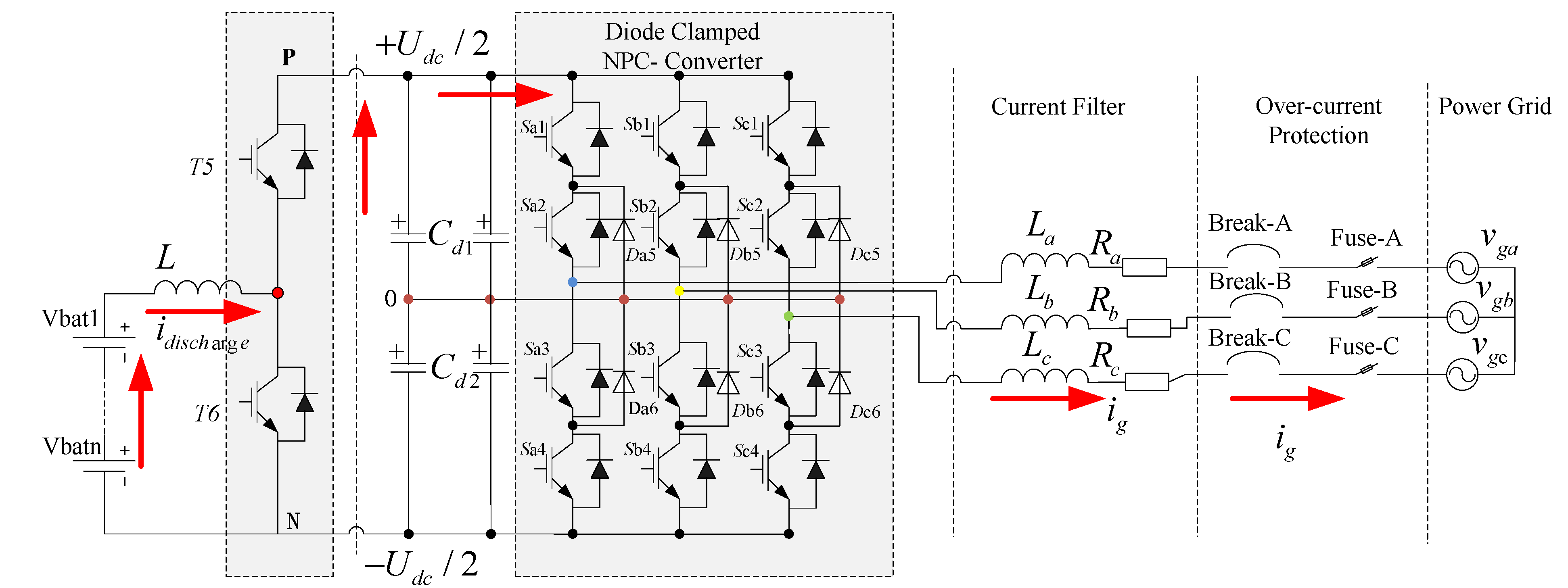
Figure 2.
Power circuit topology of the ERLPABTS using the NPC-VSC converter.
Figure 2.
Power circuit topology of the ERLPABTS using the NPC-VSC converter.
In summary, the key advantages of the proposed three-level converter in ERLPABTS are: it can handle higher and multi-level voltages with low total harmonic distortion (THD), it has a, low power transistor voltage rating requirement, and it eliminates the need for complicated filters or bulky and low efficiency isolation transformers. All of these features make the improved power circuit topology superior to that of the conventional system.
2.2. Operation Principle
The detailed schematic power circuit topology of the improved NPC-based three-level grid-connected system for ERPBPTS is shown in
Figure 2, It is different from the conventional two-level converter in [
11], because there are a total of twelve additional power transistors, and six additional voltage clamped power diodes. The ERLPABTS, therefore, has three output voltage levels: +
UDC/2, 0, and −
UDC/2. Due to the merits of a three-level converter, a simplified L type interface filter might be adopted for current filtering. A bi-directional buck and boost chopper is used for the charging and discharging current control of the power battery pack.
The operating principle of the proposed power circuit is described as follows: when the discharging current test experiment is performed, the DC-DC converter functions as a boost chopper and T6 is switched ON and OFF with the PWM. A constant charging current is obtained via the bypass diode of T5, which causes an increase in the DC-link voltage. The power transistor would be damaged through the high-voltage break down if it were not properly controlled. This energy is released to the power grid through a three-level NPC converter system. An energy balanced control strategy between the DC-DC converter and the DC-AC converter would be the most important consideration. In this way, the discharging energy could be recovered effectively, which could realize a high resolution discharging current test at the same time. A current filter, over-current protection devices, and fast-acting fuses are also used for protection. In summary, the control part of the system includes two branches: the first is the controller design for the non-isolating DC-DC boost chopper, and the second is the controller design for the energy recovery control of the ERLPABTS.
Considering the time response requirement of ERLPABTS, the instantaneous charging and discharging current control capability of the power battery pack must be evaluated. The traditional proportional and integral (PI) controller in PABPTS cannot satisfy the dynamic parameter requirements of the battery testing system. Sliding mode control (SMC) has the advantages due to its insensitivity to modeling error, variation on the parameters, and external disturbance. Moreover, sliding mode control can provide much faster dynamic response, especially in the unfixed structure and time-variant of a grid connected inverter. Therefore sliding mode control could obtain better performance than a conventional PI controller in this application.
4. Simulation Results and Discussion
Simulations for integrating the three-phase NPC inverter with the distribution grid using an
L filter interface in a Powersim 9.0 environment are carried out in order to describe and validate the capability of the proposed control scheme. The improved composite power circuit for ERPBTSs is verified through these simulations. The model is co-simulated using Matlab/Simulink and PSIM9.0 via a simcoupler block. The power circuit is established in Psim 9.0 environment and the control algorithm is realized in Simulink. The configuration and control block diagram of the system are shown in
Figure 3, and the electrical parameters used for the simulation can be found in
Table A1 and
Table A2 in the
Appendix. The simulation study is performed with three main objectives in mind:
- (1)
To demonstrate the feasibility of the proposed control scheme for the composite power circuit.
- (2)
To verify the merits of reduced total harmonic distortion of a grid-connected current by using the proposed scheme and an optimized switching table in a three-level VSC converter.
- (3)
To realize the performance of the current decoupling scheme and the proposed sliding mode controller provided in Equation (6).
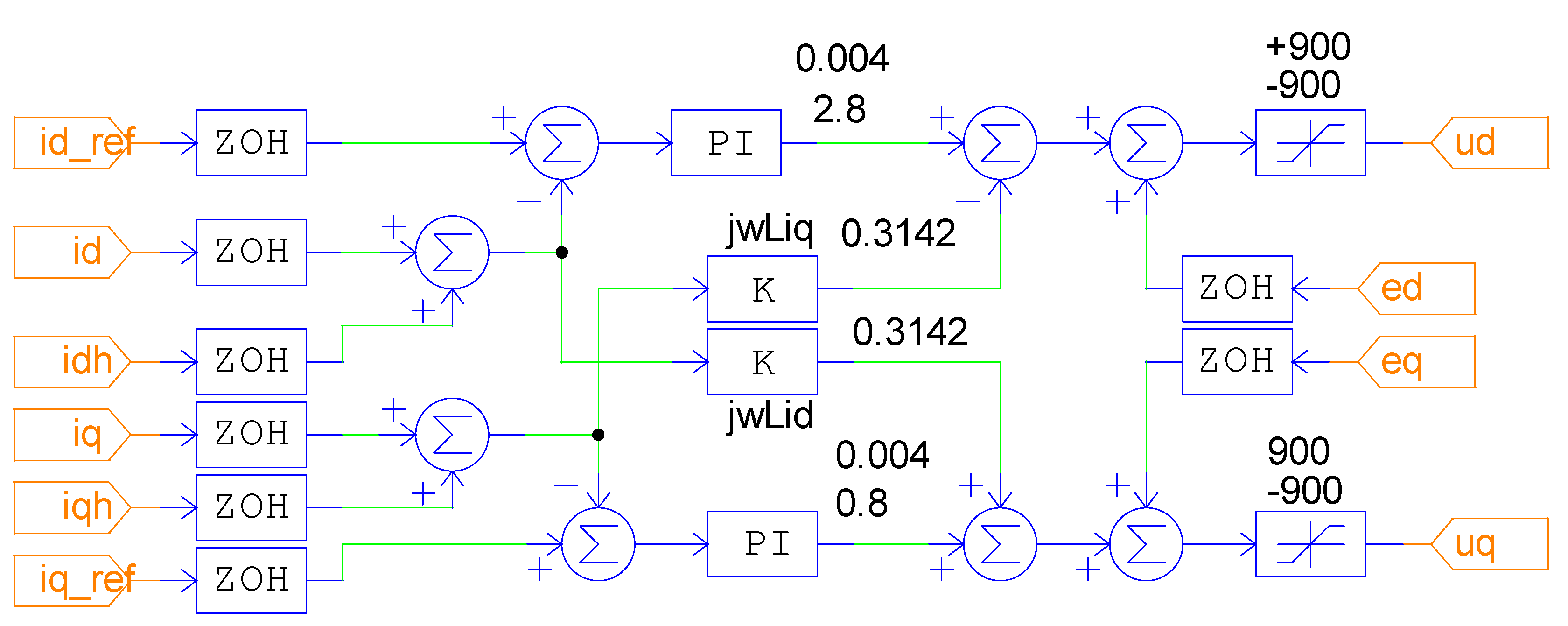
Figure 4 shows a PI control diagram of the composite power circuit for ERPBTS. The gain (
k) and time constant (
T in seconds) of the PI controller in a discharging control test are set to (
kp = 0.04,
T = 0.012). The transfer function of the PI controller used for
id and
iq control is shown in Equation (11). The PWM duty cycle is calculated using Equation (9). Two signal generators are needed to obtain the positive and negative output sinusoidal waveform. The space vector voltage to be synthesized is realized by selecting a particular voltage vector depending on the composite voltage vector’s present location:
In this section, in order to verify the performance of a different controller, we will show the simulation results for the improved composite power circuit for ERLPABTS using sliding mode control and the PI controller method, respectively.
Figure 4.
Inner active and reactive current component control using PI method.
Figure 4.
Inner active and reactive current component control using PI method.
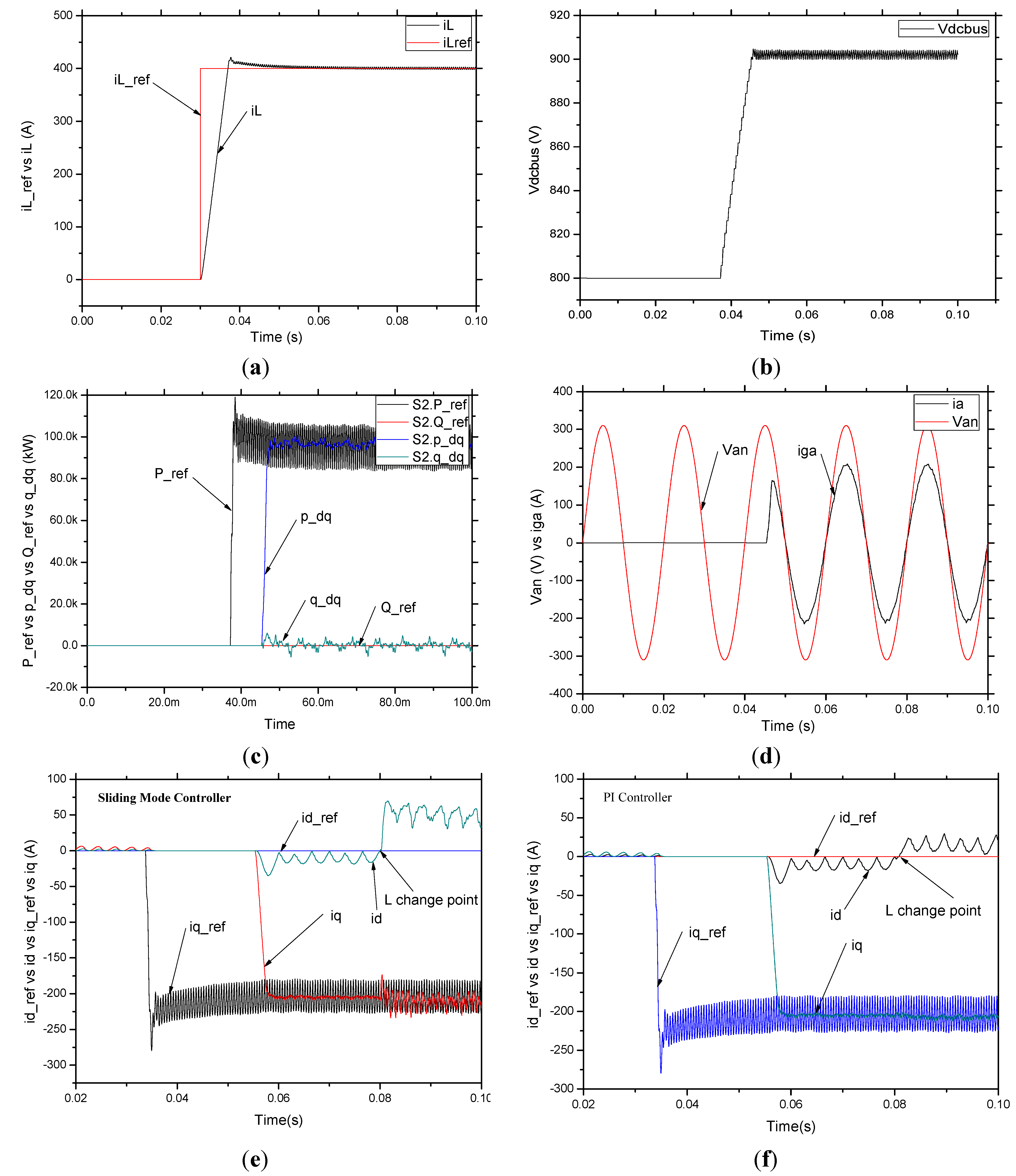
Figure 5a shows the waveform of the reference discharging current and feedback current. A step-forward reference current of 400 A is given at 0.03 s and the feedback current keeps track of its reference current with a peak value of 10 A overshot 20 ms later. This demonstrates the feasibility of the proposed scheme.
Figure 5b gives the waveform of a dc-link voltage
vdc that is set to 900 V using a switch that enables and disables PWM modulation to keep the dc-link voltage constant. The initial dc-link capacitor voltage is pre-charged to 800 V to prevent an instantaneous charging current when powered on. It can be clearly seen that the dc-link voltage remains steady and stable.
Figure 5c shows the waveform of the active and reactive powers (P_ref, Q_ref) reference where the active power (P_ref) is given by Equation (8) and the reference reactive power (Q_ref) is set to 0 to realize unity power factor control.
It can be seen that there is a time difference between the reference active power and the feedback active power which is due to the dc-link voltage. The simulation test showed that the grid-connected NPC-inverter starts to work only when the voltage reaches 900 V, and it takes 10 ms to charge from 800 V to 900 V. The reference active power is 96 kW, and the feedback active power can effectively keep track of its reference value.
Figure 5d provides the time response of the grid-connected phase current (
iga) and the grid voltage (
vga). It can be seen that the phase-current is almost in phase with the phase voltage, and that a unity power factor control is realized in the three-phase NPC inverter.
Figure 5e shows the time response of the active and reactive currents (
id,
iq) when using a sliding mode controller and PI controller (
Figure 5f). The active and reactive current references are given by Equation (9) and it is found that the feedback current could track the reference current very well. However, there is steady state error (~5 A) in this situation. The peak-to-peak active current value (
ip-p) is about 50 A. In order to compare the result when using different controllers, an extra inductor of 0.5 mH is added to the system at 80 ms, and is used to simulate the un-modeled parameter variations. It can be clearly seen that the active and reactive current components (
id,
iq) are influenced from 0 A to 50 A. The active and reactive current components when using the sliding mode controller vary from 0 A to −25 A, which is half of the variation when using the PI controller. This demonstrates that the proposed controller is insensitive to parameter variations, and is superior to the conventional PI controller.
Figure 5.
Simulation results of the proposed scheme. (a) Time response of reference discharging current and feedback current; (b) Time response of dc-link voltage; (c) Time response of reference active and reactive power; (d) Time response of the grid-connected phase current (iga) and grid voltage (vga); (e) Time response of the active and reactive currents (id, iq) using a sliding mode controller; (f) Time response of the active and reactive currents (id, iq) using PI controller.
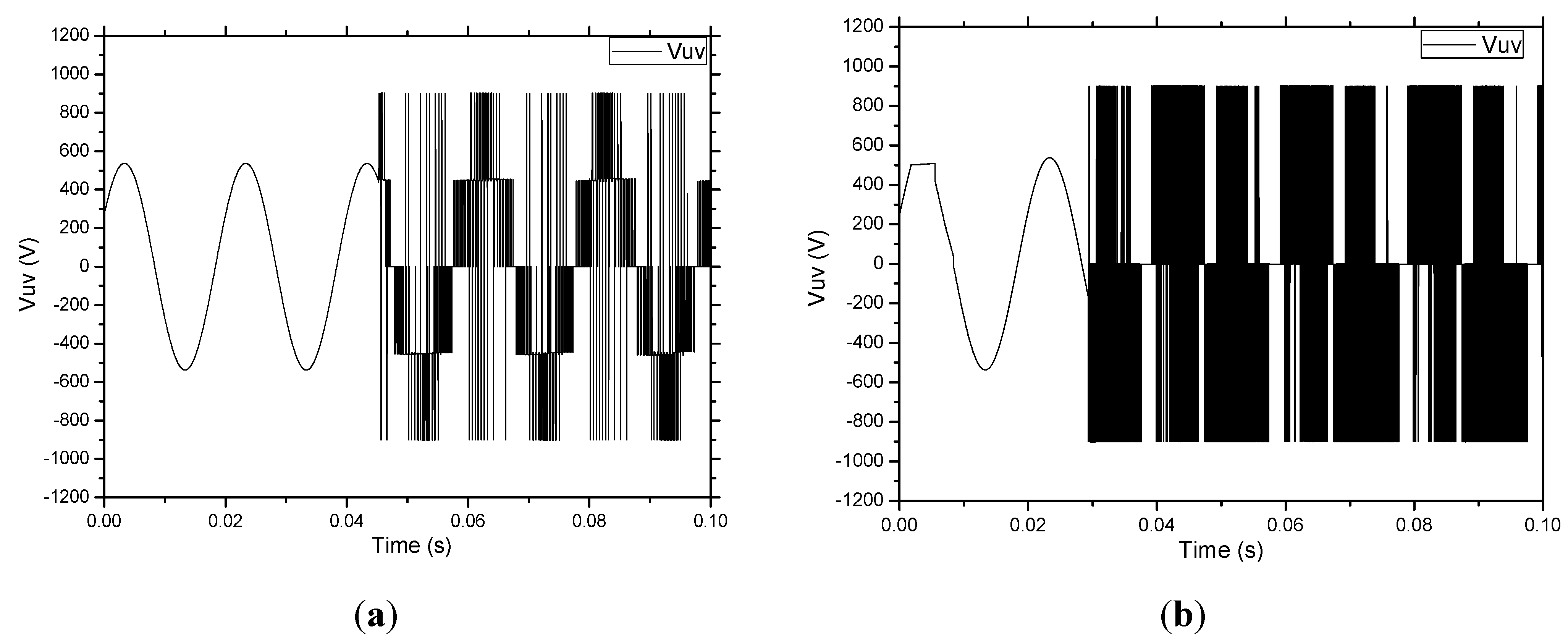
Figure 6a shows the time response of the line-to-line voltage using a three-level converter without a transformer, while
Figure 6b gives the time response of the line-to-line voltage using a two-level converter. We can see that the voltage in
Figure 6a is more sinusoidal due to its multiple output levels.
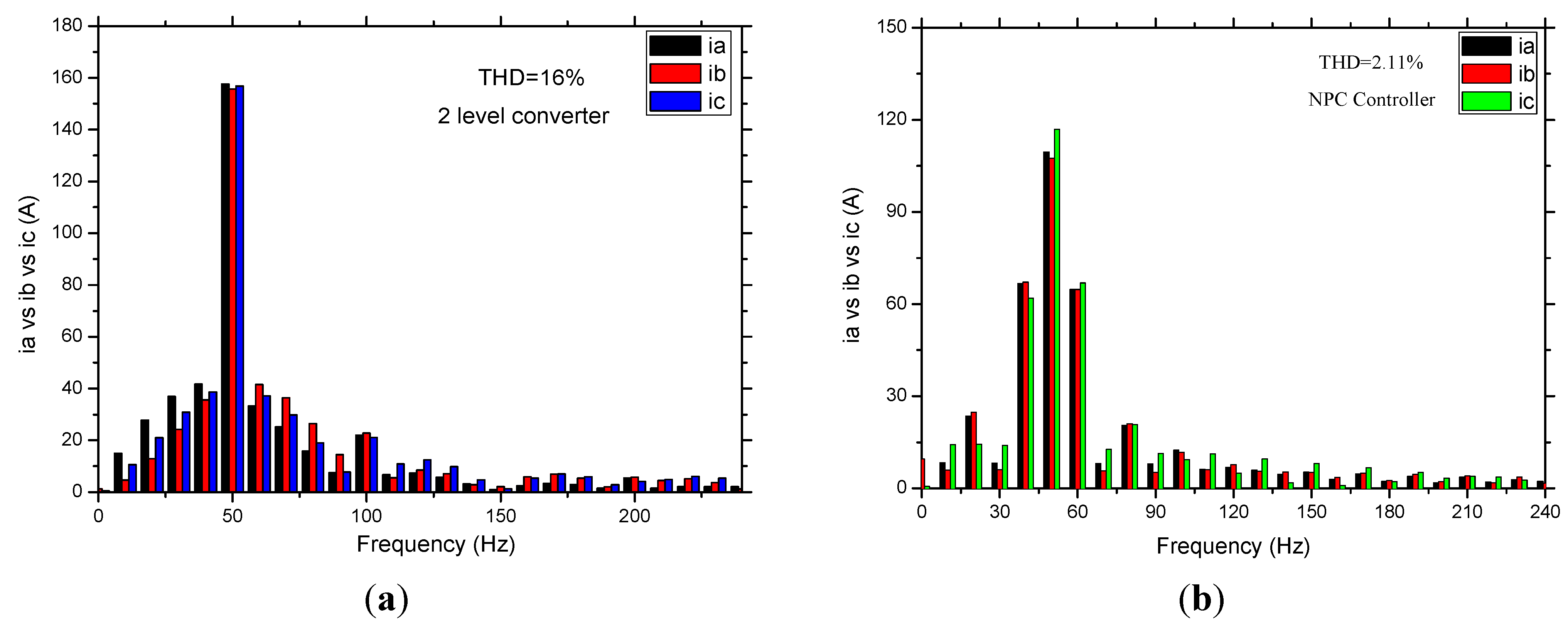
Figure 7a illustrates the harmonic distribution of the phase current using a conventional two-level inverter, and
Figure 7b shows the NPC based three-level power converter. The conventional two-level converter has more harmonics since its total harmonic distortion is 16% while that of an NPC-based three-level VSC converter is only 2.11%.
Figure 6.
Line-to-line output voltage of the (a) three-level NPC-VSC converter and (b) two-level converter.
Figure 6.
Line-to-line output voltage of the (a) three-level NPC-VSC converter and (b) two-level converter.
Figure 7.
Harmonic distribution of the (a) three-level NPC-VSC converter and (b) two-level converter.
Figure 7.
Harmonic distribution of the (a) three-level NPC-VSC converter and (b) two-level converter.
5. Experimental Section
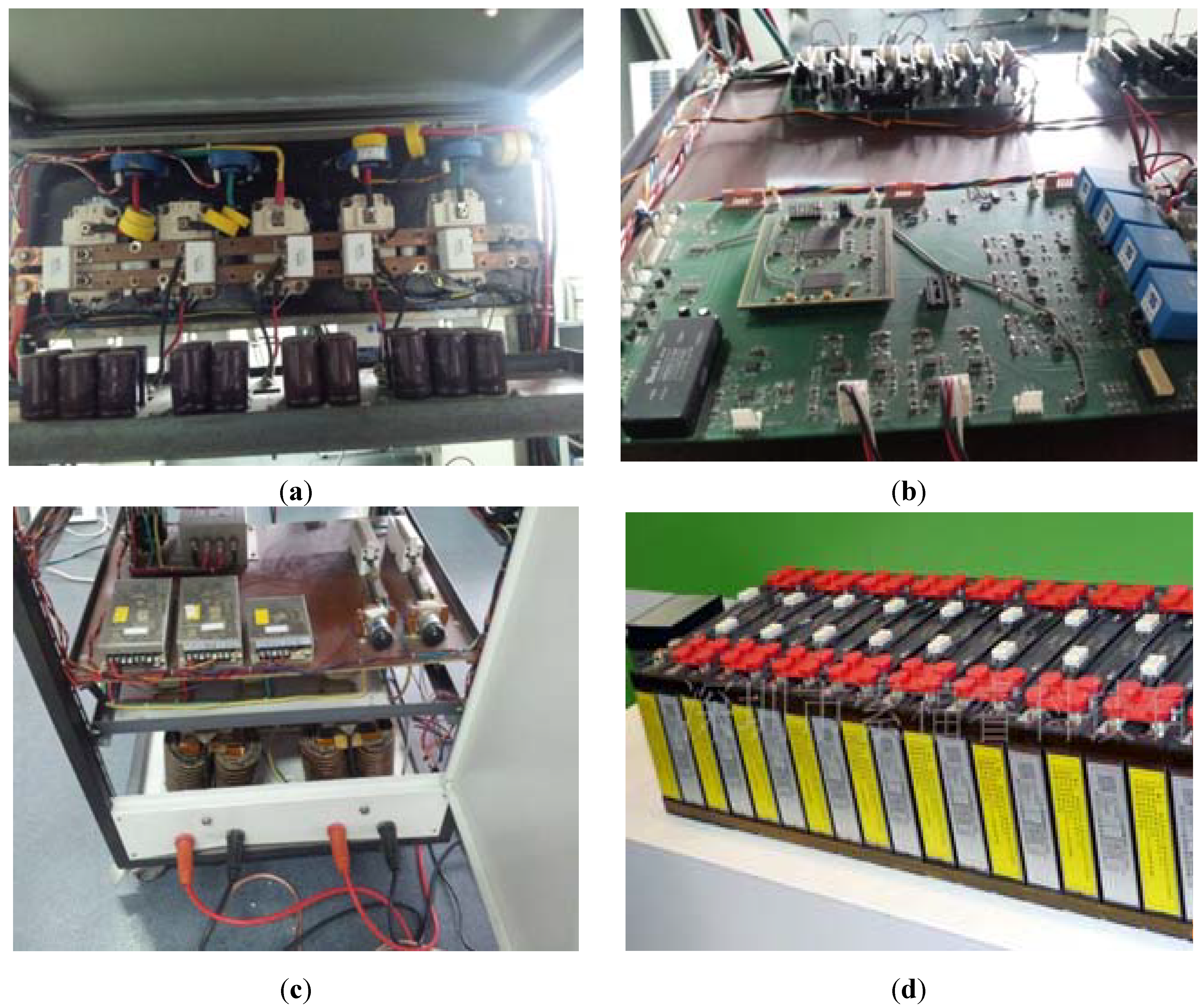
A three-level NPC-VSC inverter, which is used for a grid-connected energy recovery Li-ion type power battery testing system experimental platform based on the DSP-TMS320LF2808, is setup to verify the proposed design. The hardware setup of the power circuit configuration of the system is shown in
Figure 8a, while the IGBT driving, protection and core control board is shown in
Figure 8b. The power input part of the two-channel ERLPABTS is presented in
Figure 8c. The Li-ion battery used for experiment is presented in
Figure 8d. System configuration of the experimental setup was illustrated in earlier sections via a block diagram, and the power transistor parameters are listed in
Table A1 and
Table A2 in the
Appendix. The control scheme can be referenced in the simulation section.
Figure 8.
The three-phase NPC inverter based ERLPABTS for the experiment. (a) Power circuit of the system; (b) IGBT driving, protection and core control board; (c) Power input of the two-channel ERLPABTS; (d) Li-ion battery used for experiment.
Figure 8.
The three-phase NPC inverter based ERLPABTS for the experiment. (a) Power circuit of the system; (b) IGBT driving, protection and core control board; (c) Power input of the two-channel ERLPABTS; (d) Li-ion battery used for experiment.
The power circuit of the PWM converter consists of six IGBT where each of the IGBT modules has two integrated IGBT blocks inside. This forms a three-phase NPC full-bridge inverter circuit and a half-bridge circuit, the electrical parameters of which are shown in
Table 1 of the
Appendix. Two Hall-effect LEM sensors (LT108-S7) and four isolation voltage sensors are used for the line currents and the DC-bus voltage detection. One high-resolution LEM sensor is employed to detect the charging and discharging currents in the DC-DC power circuit. A total of fourteen PWM output signals are required in the proposed scheme of which twelve are used for the three-phase NPC converter, while the others are used for the buck-boost chopping DC-DC converter. An optimized switch table for PWM generation is used for the attenuation of the active and reactive current components on the grid side, while the phase lock loop (PLL) control algorithm is used to obtain the precise angular information of the synthesized voltage vectors.
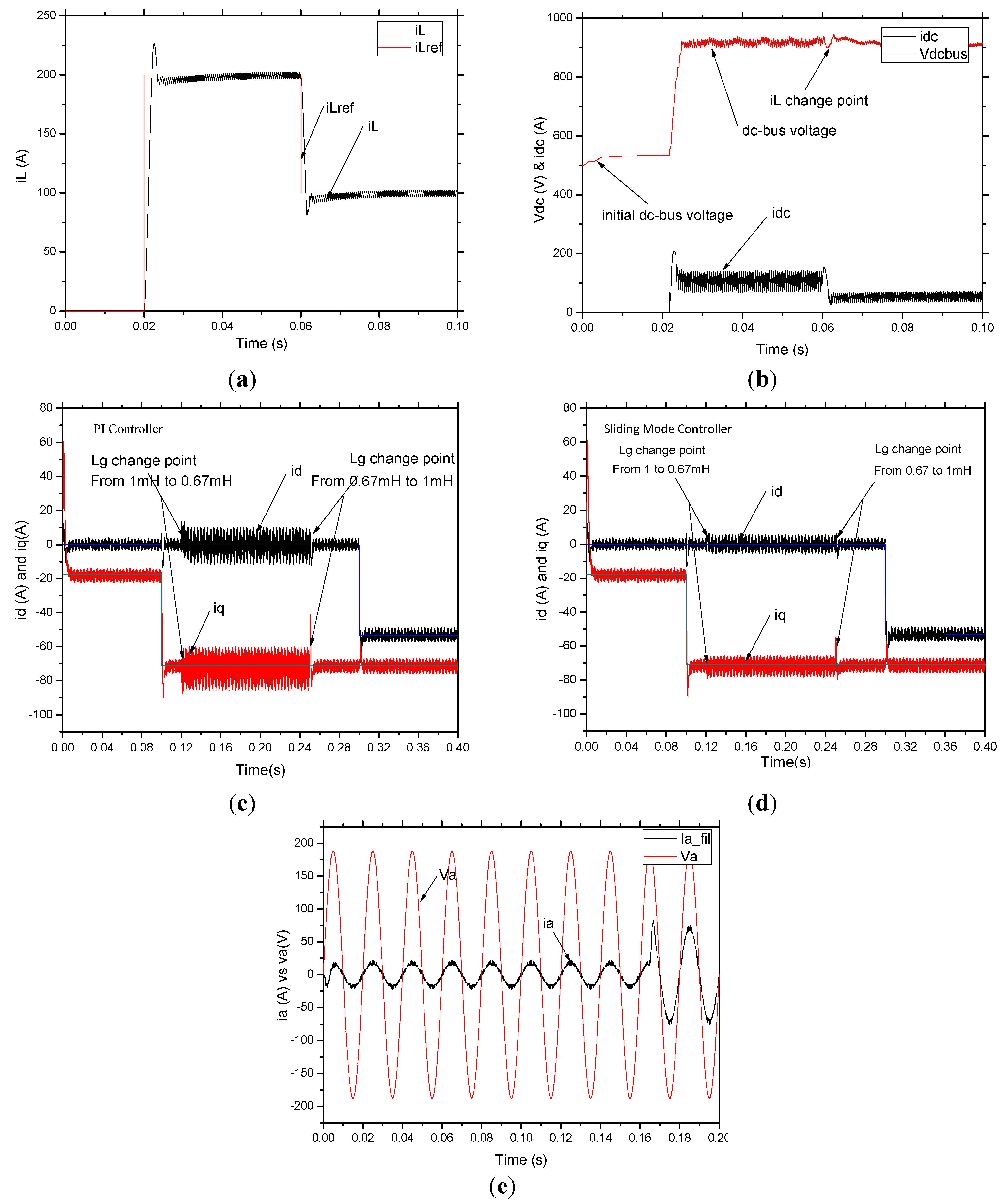
The experiments are implemented by changing the reference discharging current of the power battery pack. A step forward discharging current of 200 A is supplied at 20 ms, which is then increased to 100 A at 60 ms. The DC-bus voltage (Vdc) is set to 900 V, and the DC-bus capacities are charged by the energy released from the boosting chopper control component which gives rise to its terminal voltage. The three-phase NPC converter stops working when the DC-link voltage falls below 900 V and it restarts when the DC-link voltage is higher than 900 V. A small band could be used to keep the DC-bus voltage stable without using a high switching frequency. The reference of the active and reactive power varies according to the discharging current and the DC-bus voltage which keeps the energy balanced both in the boost chopper and inverter sides. The discharge energy of the battery power testing is therefore restored to the power grid with high efficiency.
The discharging current response of the power battery pack is shown in
Figure 9a. The feedback current initially peaks at 225 A and then keeps track of the reference current after 10 ms when given a reference current of 200 A at
t = 20 ms. The feedback current initially drops to less than 100 A and then converges back to the command value 10 ms later when a step-down discharge current of 100 A is given at
t = 60 ms. An instantaneous inrush current is caused by the pure inductor load on the boost chopper side. A smaller filter inductance has drawbacks due to the large current ripples, but a large filter inductance results in a short time response and a large volume. An inductance of 4 mH is adopted for this experiment.
The time response of the DC-bus voltage is shown in
Figure 9b. The initial DC-bus voltage is set to 500 V which starts to increase at
t = 20 ms and reaches 900 V about 2.5 ms later. The DC-bus voltage starts to increase again at
t = 60 ms when a step-down current reference is given which is due to the reduced load on the DC-bus.
Figure 9c and d illustrates the experimental results of the active and reactive current components (
id and
iq) when the grid-connected interface inductor changes under the PI and SMC control methods, respectively. Compared with
Figure 9c, the active and reactive current components in
Figure 9d are influenced less by the grid-connected inductance variations (±10 A in PI and ±6 A) when the inverter side inductor (
ig) changes from 1 mH to 0.67 mH at 120 ms and from 0.67 mH to 1 mH at 250 ms, This demonstrates that by using the sliding mode controller, the system is insensitive to the parameter variations in the system. The improved control method could offer better robustness than the conventional method.
Figure 9e illustrates the time response of the active and reactive current components in the three-phase NPC converter. It shows that the reactive current component (
id) converges to zero, and that the active current feedback (
iq) follows its reference component (
iqref) very well when the DC-bus voltage increases to 900 V.
To summarize, the experimental results confirm that the proposed scheme is not only feasible, but also valid and applicable. The proposed scheme could greatly improve conventional composite power circuits since the proposed novel system is more compatible, lighter, and less total grid current harmonic distortion.
Figure 9.
(a) Experimental results of time response vs. discharging current (iL); (b) Experimental results of time response vs. dc-bus voltage (Vdcbus); (c) Experimental results of active and reactive current components (id and iq) when the grid connected interface inductor changes by using the PI method; (d) Experimental results of active and reactive current components (id and iq) when the grid-connected interface inductor changes from 0.67 mH to 1 mH by using SMC method; (e) Experimental results for grid-connected current (ia) and grid voltage of the system (van).


