Article

Modeling of Step-up Grid-Connected Photovoltaic Systems for Control Purposes

by
Adriana Trejos
1,*,
Daniel Gonzalez
2 and
Carlos Andres Ramos-Paja
2
1
Instituto Tecnologico Metropolitano, Medellin 05001000, Colombia
2
Universidad Nacional de Colombia, Medellin 05001000, Colombia
*
Author to whom correspondence should be addressed.
Energies 2012, 5(6), 1900-1926; https://doi.org/10.3390/en5061900
Submission received: 27 February 2012 / Revised: 16 May 2012 / Accepted: 1 June 2012 / Published: 18 June 2012
(This article belongs to the Special Issue Solar Energy Systems and Materials)

Abstract

:
This paper presents modeling approaches for step-up grid-connected photovoltaic systems intended to provide analytical tools for control design. The first approach is based on a voltage source representation of the bulk capacitor interacting with the grid-connected inverter, which is a common model for large DC buses and closed-loop inverters. The second approach considers the inverter of a double-stage PV system as a Norton equivalent, which is widely accepted for open-loop inverters. In addition, the paper considers both ideal and realistic models for the DC/DC converter that interacts with the PV module, providing four mathematical models to cover a wide range of applications. The models are expressed in state space representation to simplify its use in analysis and control design, and also to be easily implemented in simulation software, e.g., Matlab. The PV system was analyzed to demonstrate the non-minimum phase condition for all the models, which is an important aspect to select the control technique. Moreover, the system observability and controllability were studied to define design criteria. Finally, the analytical results are illustrated by means of detailed simulations, and the paper results are validated in an experimental test bench.

1. Introduction

Power generation systems based on alternative energy sources have become stronger options to address the continuous power demand and the initiative to reduce the use of fossil fuels. One of the most suitable option concerns photovoltaic (PV) modules, particularly for low power levels [1]. The innovation on photovoltaic energy and power electronics fields makes this technology an important research area, particularly in modeling and control techniques. The design of a controller capable of rejecting disturbances on the PV module (PVM) and the load represents one of the main challenges in the implementation of this kind of systems, where it is essential to select an appropriate model for the PVM, the power electronics interface, and the disturbance sources. Several PVM models have been reported in literature: [2] presents a non-linear model of mismatched PV fields, while in [3] a double exponential model is introduced. In [4], the single diode PVM model and the diode equivalent circuit are discussed, and a piecewise linear model is proposed. Similarly, in [5] a simplified model is proposed using only parameters provided by manufacturer’s specifications to avoid the use of numerical methods. Moreover, to develop control strategies, more simple models have been proposed based on differential resistance [6], Norton [7], and Thevenin [8] circuital approximations.
Due to the strong non-linear electrical behavior of the PVM [2,9], there exists an optimum operating point in which the PVM produces the maximum power, named Maximum Power Point (MPP). The PVM voltage must be defined to achieve the MPP, which significantly changes depending on the irradiance conditions. Therefore, it is not possible to predict off-line the MPP, which must be calculated on-line [10,11]. Such a condition has been addressed in literature by introducing a special controller to track the MPP on-line, named Maximum Power Point Tracking (MPPT), aimed at maximizing the power extracted from the PVM [6,11]. The most commonly used MPPT solutions are the perturb and observe (P&O) and incremental conductance (IC): the P&O technique is widely adopted due to its implementation simplicity [10,12]. It tracks the MPP by periodically perturbing the control variable (PVM voltage) and comparing the instantaneous PVM power after and before the perturbation [6], selecting the sign of the next voltage perturbation that guarantee a PVM power increment. Instead, the IC technique tracks the operating point in which the derivative of the PVM power with respect to the voltage is zero, since such a condition corresponds to the MPP. The main drawbacks of the IC technique consists in the highly accurate current sensor required and the increased implementation complexity in comparison with the P&O, but the IC could provide a more accurate MPP calculation depending on the current sensor dynamical response and steady-state error [10].
Despite the adopted MPPT algorithm, a power converter is required to interface the PVM and the load to drive the PVM to the MPP. The classical solutions reported in literature are the single and double stages architectures. 
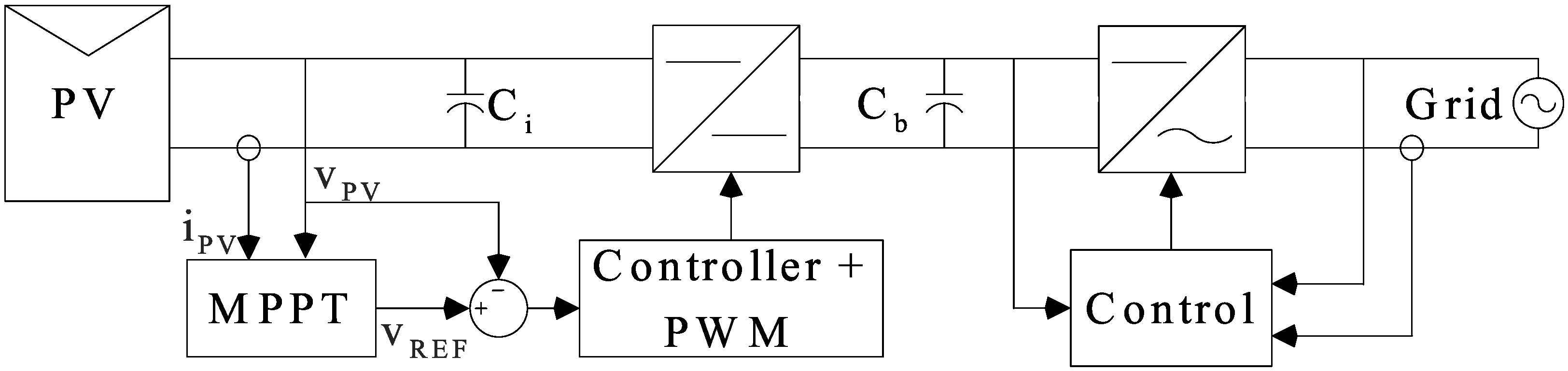
Figure 1 shows the Double Stage (DS) architecture, which is composed by a DC/DC converter controller by the MPPT algorithm, and a DC/AC converter regulated to inject the power into the grid and to regulate the DC-bus voltage, i.e., bulk voltage. Such DS solution is widely adopted since it makes possible to simultaneously follow the MPP and provide power factor correction [12]. The DS architecture of Figure 1 also considers the DC/DC converter controller, which regulates the PVM voltage in agreement with the MPPT command. Moreover, the DC/DC converter adopted in DS solutions commonly consists in a step-up topology to match the high-input voltage required by classical grid connected inverters from the low-voltage operating conditions exhibited in PVM.
Figure 1. Double stage-grid connected PV architecture.
Energies 05 01900 g001
In addition, double-stage PV systems connected to the grid are exposed to perturbations generated by the DC/AC converter (or inverter) operation in mono-phase systems, but also in non-perfectly balanced three-phase systems. Moreover, classical photovoltaic inverters act on the input current to regulate the voltage at their input terminals, but more common and simple inverters lack such a feature. In the first case, the inverter properly regulates the DC component of the voltage at the bulk capacitor that interfaces the DC and AC stages, named C b in Figure 1, but a sinusoidal perturbation on the bulk voltage is generated at double of the grid frequency, whose magnitude is inversely proportional to the bulk capacitance [12,13]. In the second case, the DC component of C b voltage is not accurately regulated and the inverter absorbs a sinusoidal current at double the grid frequency, generating an undesirable voltage oscillation that exhibits different frequency harmonics at the bulk voltage, i.e., the DC/DC converter output terminals, with an amplitude inversely proportional to the bulk capacitance [14]. In both cases the DC/DC converter output is exposed to voltage perturbations that could be transferred to the PVM terminals. Such a condition degrades the MPP calculation, which is particularly critical in the classical solutions that perturb the DC/DC converter duty cycle, since PVM voltage oscillations with magnitude Δ V b / M ( D ) occurs, where Δ V b represents the magnitude of the bulk voltage oscillation and M ( D ) represents the DC/DC converter voltage conversion ratio. Therefore, a common practice to deal with such a problem is to reduce Δ V b by using large bulk capacitances, requiring electrolytic capacitors to avoid the high cost of large ceramic or polyester capacitor banks. But the use of electrolytic capacitors significantly reduces the reliability of the system [13,15], creating a bottleneck.
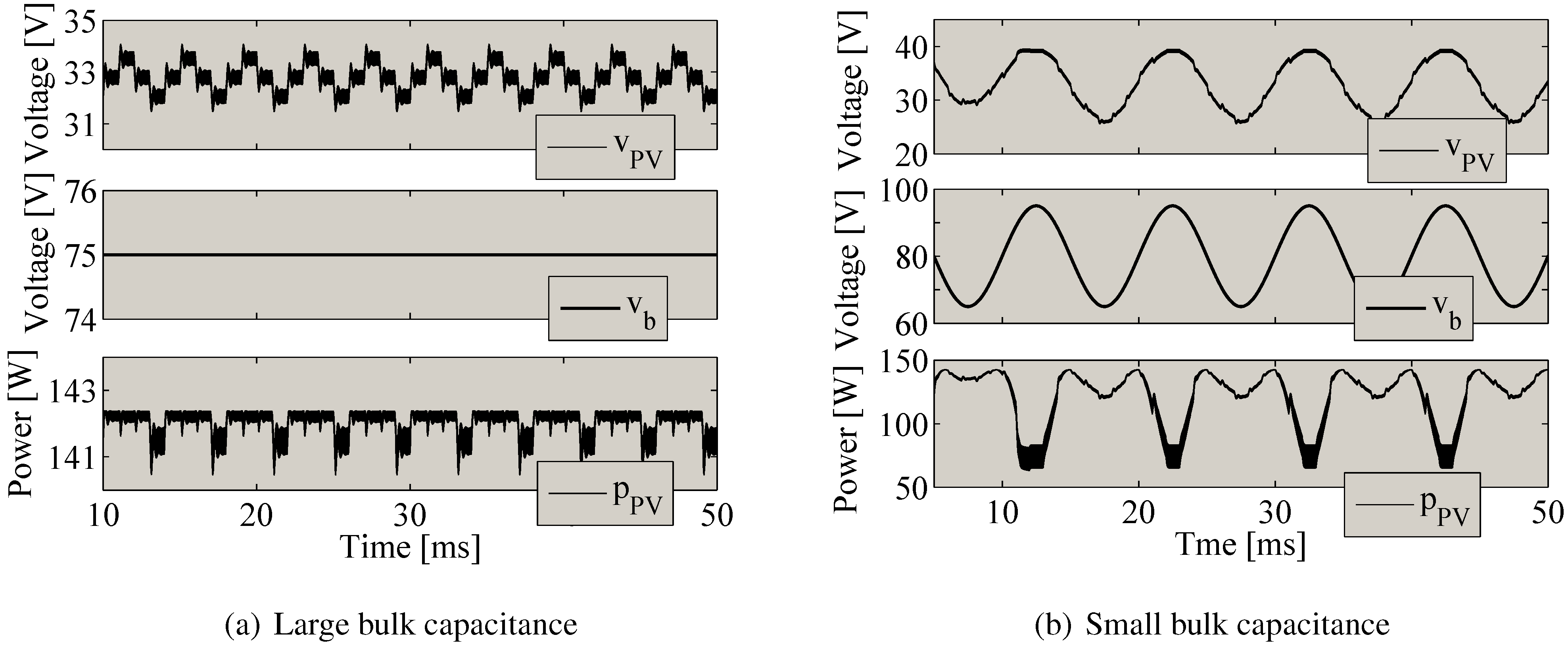
Figure 2 illustrates the impact of the bulk capacitor in the MPPT performance: a PV system, composed by two BP585 PV panels in series and a boost converter, is simulated adopting a P&O MPPT algorithm for large and small C b . v P V and p P V represent the voltage and power of the PV array, while v b represents the bulk voltage. Figure 2(a) shows that, using a large bulk capacitor that significantly mitigates Δ V b , an accurate tracking of the MPP is ensured, extracting the maximum power available. Instead, Figure 2(b) shows the PV system simulation considering a small bulk capacitor that generates a voltage oscillation with magnitude Δ V b = 40 % , and such an oscillation is transferred to the PV voltage, introducing errors in the MPP calculation that significantly degrade the power extracted from the PV array. Therefore, an additional controller that rejects such a bulk voltage perturbation must be introduced.
Figure 2. Grid-connected PV system with duty cycle perturbation.
Energies 05 01900 g002
To analyze the PV system behavior under the previous conditions, the bulk capacitor and grid-connected inverter are modeled in the literature by means of two approaches: first, when the inverter accurately regulates the DC component of the bulk voltage, they are modeled by means of a voltage source [12] that allows to analyze the impact of the bulk voltage oscillations on the system dynamics. Second, when the inverter does not regulate the DC component of the bulk voltage, they are modeled by means of a Norton equivalent [6] that allows to analyze the impact of the current-based perturbation on the system response. Both modeling approaches are widely accepted in the literature for grid-connected inverters operating in open loop (Norton equivalent) and closed loop (voltage source).
Concerning the DC/DC converter modeling, it is common to adopt ideal models for designing control and MPPT techniques [11,12,16,17] to avoid complex equations derived from considering parasitic elements. Such simple models are useful to provide proof-of-concept simulations of new control strategies. But to achieve more accurate controllers, which is particularly important for experimental cases, at least the parasitic resistances of the passive elements must be considered. Moreover, the parasitic resistances significantly impact the system dynamics, introducing additional zeros and increasing the damping to DC/DC converter transfer functions.
To overcome the bottleneck created by the large bulk capacitor required in classical PV systems, it is essential to design accurate PVM voltage controllers to reject bulk voltage oscillations from the PVM terminals. Such a controller action allows to adopt non-electrolytic bulk capacitors, increasing significantly the PV system reliability without impacting the overall cost. The aim of this paper is to provide well-founded, trustworthy, and ready-to-use mathematical models of grid-connected PV system to support the design of PVM controllers. The proposed models are formulated in state-space representation to simplify its use in system analyses, to design linear or non-linear controllers by means of time or frequency based techniques, and to be easily implemented in simulation environments like Matlab, Mathematica or Maple. The models are based on circuital representations of PV systems widely adopted in literature, even in recent publications [18,19]. Moreover, the modeling approach considers both Norton equivalent and voltage source representations of the bulk capacitor interacting with an inverter. To cover a wide range of applications, the models are derived considering both ideal and realistic DC/DC converters, i.e., with and without parasitic resistances, respectively. In addition, the model’s controllability and observability are analyzed to provide design guidelines for the DC/DC converter to allow the implementation of controllers and observers in real applications. Such analyses will help to reduce the sensors and conditioning circuits, reducing in this way the PV system costs and supporting the implementation of advanced control techniques, e.g., model predictive control. In particular, an observer for the input current of the DC/DC converter is very interesting, since it can be used to replace PVM current sensors classically used to calculate the instantaneous PVM power for the MPPT controller.
A boost converter, operating in Continuous Conduction Mode (CCM) [20], was considered in this work since it is the most common step-up topology adopted in grid-connected PV systems [6,7,11,12,16,17,18,19]. The boost topology requires a bulk voltage higher than the PVM voltage, which is commonly ensured by the selection of the DC/AC stage [6,18]. Moreover, advanced control strategies, such as predictive control, can be used to avoid the converter instability in such a condition [21]. Similarly, the inductor of the boost converter is normally designed to operate in CCM [6,7,18,19] since Discontinuous Conduction Mode (DCM) causes larger PVM voltage ripple [22,23] and oscillations around the MPP [24], which decrease the effective power injected into the grid.
The boost topology also provides higher electrical efficiency than other classical converters for the same PVM and bulk voltages, e.g., buck-boost [25]. But due to the non-minimum phase of the duty-cycle-to-output voltage transfer function of the boost converter [26], its output voltage is classically regulated by means of cascade current and voltage control loops [20]. Such a non-minimum phase condition increases the complexity of the controller design due to stability issues [27,28]. This paper demonstrates, by means of analytical expressions, that the duty-cycle-to-PVM voltage transfer function does not exhibit non-minimum phase behaviors for any condition, which guarantee the effectiveness of a direct PVM voltage controller. Such a result puts in evidence that cascade current-voltage controllers for PV systems, as the one reported in [29], are not required for stability. Moreover, avoiding inner current controllers has multiple benefits: taking into account that PV-voltage based MPPTs are more stable than PV-current based MPPTs due to possible saturations of the PVM current caused by fast changes on the irradiance, the PVM voltage regulation is widely adopted to implement the MPPT technique [18,30]. In this way, a direct PVM voltage control with the duty-cycle limits the control bandwidth up to 1/5 of the switching frequency [31]. Instead, using a cascade connection of current and voltage controllers, the maximum bandwidth of the PVM voltage regulation is strongly reduced since the bandwidth of an external control loop (i.e., voltage loop) must be smaller than 1/5 of the inner loop bandwidth [32] (i.e., current loop), or even smaller than 1/10 of the inner control loop bandwidth as suggested by more conservative authors [33]. Therefore, it is desirable to avoid the inner current loop to improve the system bandwidth, which eventually improves the MPP tracking speed since the MPPT perturbation period can be reduced [6].
In addition, the bandwidth required by the MPPT current sensor is in agreement with the MPPT perturbation period, which must be larger than the settling-time of the PV system small-signal model [6]. Therefore, the low-bandwidth current sensor required by the MPPT is cheaper and easier to implement in comparison with a high-bandwidth current sensor required for control purposes, like the one presented in [18]. Moreover, it is clear that to implement a cascade control structure requires to design two controllers instead of only one as in the direct PVM voltage control. Similarly, the implementation of a single voltage controller requires fewer elements and consumes less energy than a cascade configuration. Therefore, it is desirable to avoid current control loops in PV systems to reduce the implementation cost and complexity.
The remain of the paper is organized as follows: Section 2 describes multiple PVM modeling approaches and selects the most suitable one for the intended control-oriented application. Section 3 and Section 4 present the modeling of the grid-connected PV system based on the Norton equivalent and voltage source cases, respectively. Section 5 presents an application example of the proposed models illustrated by means of PSIM simulations, where the controllability and observability analyses are validated through a small-signal observer design. An experimental validation of the analytical results is presented in Section 6, where a controller designed by means of the proposed models interacts with a P&O MPPT controller in a real photovoltaic system. Finally, Section 7 concludes.

2. Modeling the Photovoltaic Module for Control Purposes

The photovoltaic cells are generally composed by layers of silicon p and silicon n. The light with particular wave length ionize the atoms of the silicon and the inner field between the positive and negative charges inside the photovoltaic device. The stronger the irradiance, the higher the interaction between the atoms and a higher potential difference is produced. To illustrate the electrical behavior of a PV module (
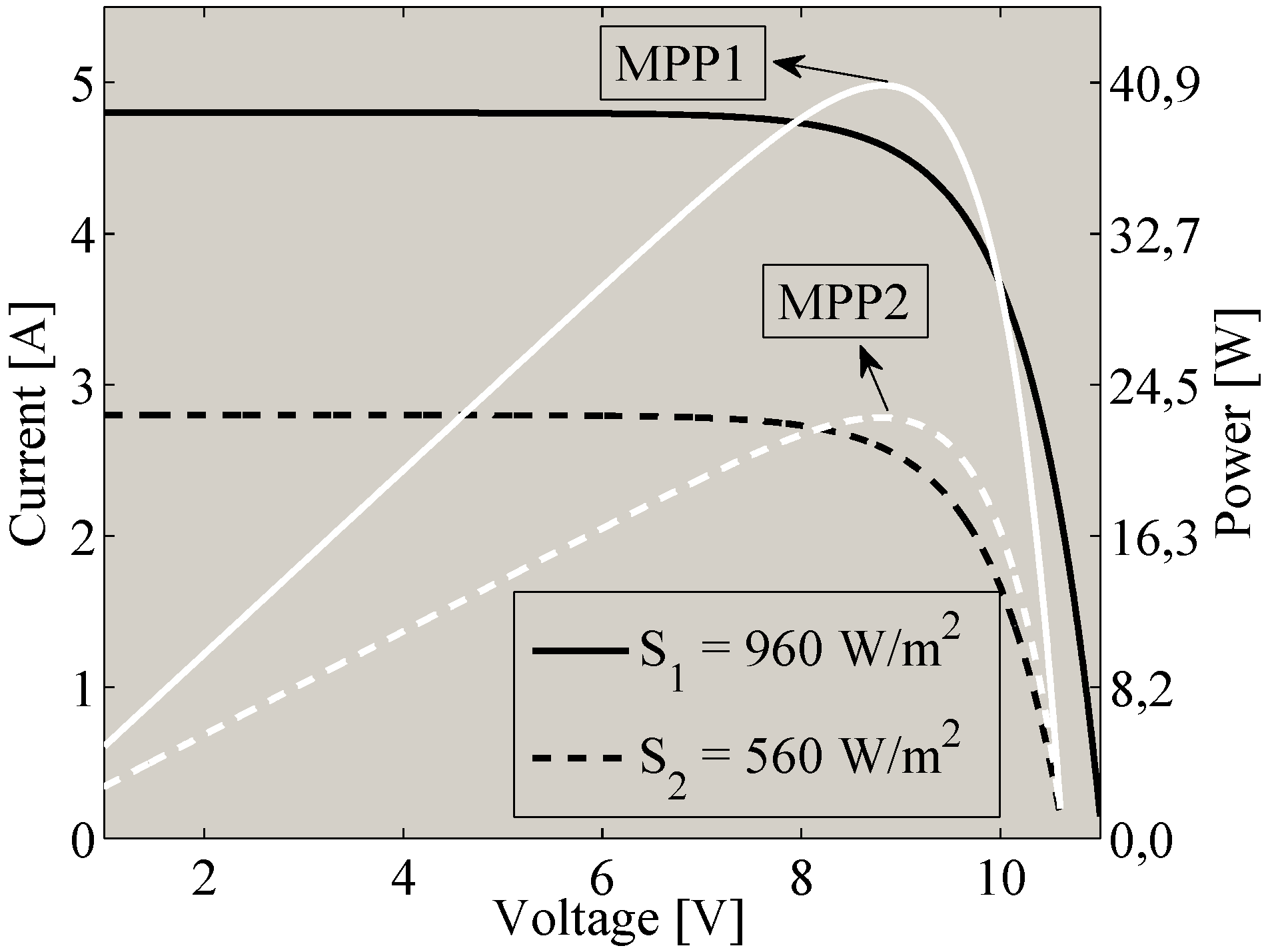
i.e., PVM) the characteristic curves of a commercial BP-585 PV module are shown in Figure 3. Since a BP-585 PV panel is composed by two PVM in series, the BP-585 PVM open-circuit voltage is equal to the half of the PV panel open-circuit voltage, while the short-circuit current for both PVM and PV panel are equal. In particular, Figure 3 presents the PVM current-voltage (I-V) and power-voltage (P-V) curves for two different irradiance levels S 1 and S 2 , where the maximum power point (i.e., MPP) for each irradiance condition is observed. In addition, it is noted that the electrical characteristic of the PVM directly depends on the irradiance, which defines an important condition for modeling the PV module.
Figure 3. I-V (black) and P-V (white) curves of a BP-585U PV module.
Energies 05 01900 g003
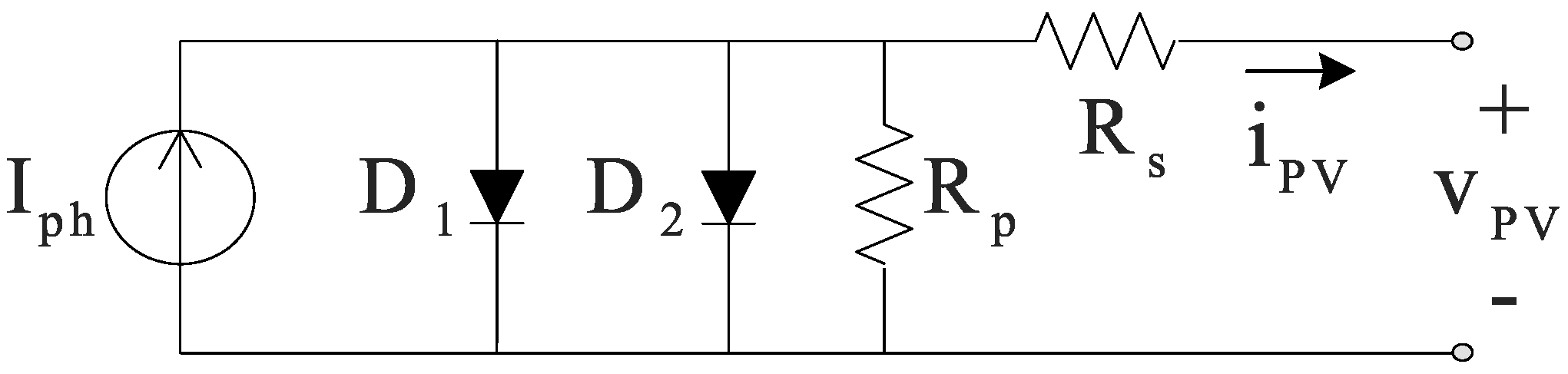
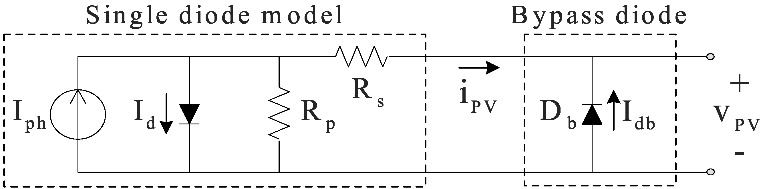
Several PVM models have been reported in literature. Such models normally consist in non-linear equations due to the physical variables involved in the PVM operation. In this way, the work reported in [2] models a monocrystalline PVM by means of a single-diode circuital model [11], including also a bypass diode D b . Such an approach, depicted in Figure 4, is used to develop complex models to analyze PV strings considering mismatched conditions [9].
Figure 4. Single-diode model of a PVM including a bypass diode.
Energies 05 01900 g004
Concerning polycrystalline PVM, the double-diode model depicted in Figure 5 is one of the most accurate models [3], but it exhibits a high complexity due to its double exponential terms. Therefore, it is common to use the single-diode model to represent both monocrystalline and polycrystalline PVM, but due to the implicit relation between voltage and current in both single and double diode models, a complex mathematical function, named Lambert-W, is required to solve the system [2], which strongly increases the calculation time in comparison with explicit models. Therefore, simplified versions of the single-diode model, neglecting parallel R p [5] and series R s [9] resistances in Figure 4, are also reported.
Figure 5. Double-diode model of a PVM.
Energies 05 01900 g005
The non-linear models previously described are useful for electrical simulation purposes and energy harvesting evaluation [9], but they introduce a high complexity in terms of control systems analysis and design. Moreover, since the main objective in PV systems is to extract the maximum power available, the PVM must be operated at its MPP, see Figure 3. Therefore, three simple modeling approaches are widely accepted in literature to represent the PVM near the MPP: differential resistance [6,12], Norton equivalent [7], and Thevenin equivalent [8].
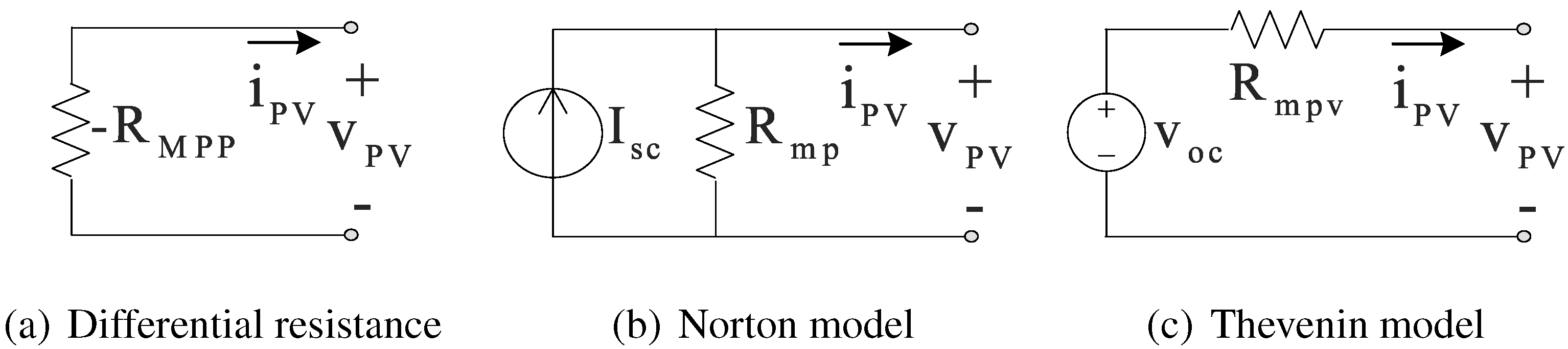
The magnitude of the differential resistance, depicted in Figure 6(a), is calculated as (1), where V M P P and I M P P represent the PVM voltage and current at the MPP. It is noted that such a resistance is negative since it models a generator. The Norton model, depicted in Figure 6(b), is calculated from the short-circuit current I S C of the PVM and the MPP characteristics ( V M P P and I M P P ). Similarly, the Thevenin model, depicted in Figure 6(c), is calculated from the open-circuit voltage V O C of the PVM and the MPP.
R M P P = V M P P I M P P
Figure 6. PVM linear models around the MPP.
Energies 05 01900 g006
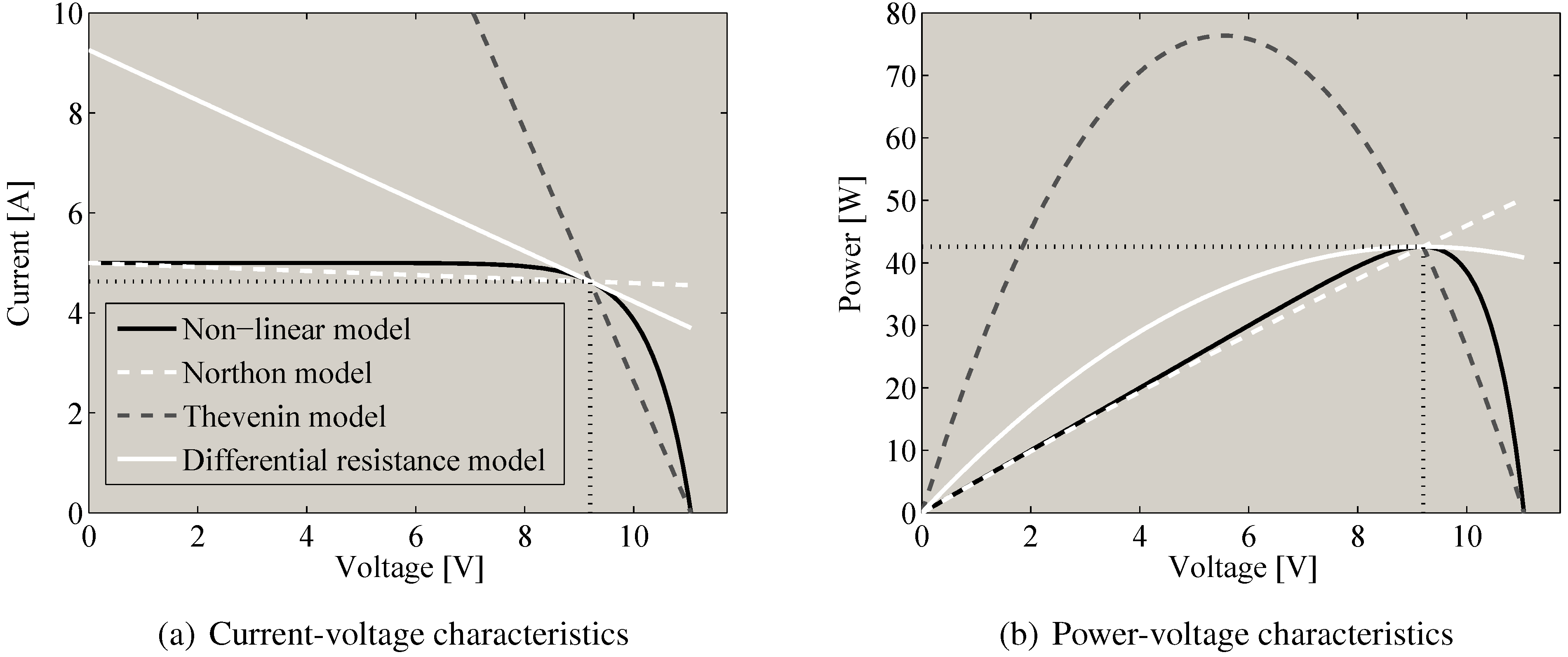
The three linear models accurately represent the PVM electrical behavior at the MPP, as illustrated in Figure 7, but it is noted that the Norton model is closer to the non-linear model for voltages lower than V M P P . Similarly, the differential resistance model fits better the power derivative of the non-linear model at the MPP. Finally, the Thevenin model is closer to the non-linear model for voltages higher than V M P P . But only the Norton and voltage source models allow to analyze the effect of environmental variables in the control system design. In this way, the Norton model involves the PVM short-circuit current, which is proportional to the irradiance [9], therefore it allows to analyze the effects of irradiance variations on the PV system. Similarly, the Thevenin model takes into account the PVM open-circuit voltage, which depends on the PVM temperature [2], then it allows to analyze thermal effects. In contrast, the differential resistance does not allow a direct analysis of environmental changes on the system.
Figure 7. PVM linear models comparison.
Energies 05 01900 g007
Since the irradiance variations have higher impact on the PV system’s electric behavior than thermal changes [34], the Norton equivalent is adopted to model the PV system, providing information about the irradiance perturbations attenuation on the PVM voltage control. Such a condition makes it possible to ensure the correct operation of the PV system, or even to design the control strategy to achieve a desired rejection level. Moreover, the single-diode model is used in the following sections to validate the analyses performed with the linear PVM model.

3. Modeling the PV System Considering a Bulk Voltage Source

This section presents the modeling of the PV system considering the voltage source representation of the bulk capacitor interacting with a closed-loop grid-connected inverter, i.e., properly regulated DC component of the bulk voltage. Two models have been developed: the first one considers an ideal DC/DC converter, and the second one considers both the inductor and capacitors parasitic resistances.

3.1. Ideal DC/DC Converter Case

The electrical scheme of this loss-free PV system is presented in Figure 8. The dynamic equations are defined to represent the system in state space, where the state variables are the inductor current and input capacitor voltage, while the system inputs are the converter duty cycle, the irradiance represented by the PVM short-circuit current, and the converter output voltage, i.e., the bulk voltage. The complete set of equations are given in (2)–(3), where v C i represents the input capacitor voltage, i L the inductor current, and d the DC/DC converter duty cycle.
Figure 8. Loss-free PV system considering a bulk voltage source.
Energies 05 01900 g008
d i L d t = v C i L - v b 1 - d L
d v C i d t = i s c C i - v C i C i R m p - i L C i
This system is clearly non-linear, therefore it is required to calculate the Jacobian matrices to obtain a linear model around the desired operating point, i.e., the MPP. The state space realization (4)–(5) is characterized by the vectors given in (6) and the set of Jacobian matrices given in (7)–(8).
X ˙ = A m X + B m U
Y = C m X + D m U
X = i L v C i U = d i S C v b C m = 0 1 T D m = 0 0 0 Y = v C i
A m = 0 1 L - 1 C i - 1 C i R m p
B m = v b 0 - 1 + d L 0 1 C i 0
It must be point out that lower case letters in the Jacobian matrixes (7)–(8) represent dynamic variables, which must be evaluated around the MPP. The constants calculated from the evaluation of the dynamic variables at the MPP are represented by upper case letters.
The equilibrium point, around the MPP, is obtained by equating (2)–(3) to zero. To validate the proposed model, a comparison between the mathematical model and the non-linear circuit frequency responses is performed by adopting the following parameters: L = 56 μH, C i = 44 μF, V C i = 33.15 V, V b = 70 V, I s c = 4.7 A, R m p = 81.87 Ω, and switching frequency f s w = 100 kHz. The circuital Bode diagrams were obtained in the power electronics simulation software PSIM adopting both the Norton equivalent and the non-linear PVM model of Figure 4 (implemented in the Renewable Energy library from PSIM), while the Bode diagrams of the PV system model were computed in Matlab. Figure 9(a) and Figure 9(b) show the mathematical model and the circuit frequency responses for the state variables, where the non-linear PV system behavior is satisfactorily reproduced. Such results show that the frequency responses of the PV system, adopting the Norton PVM model, are superimposed with the PV model frequency responses. Instead, the frequency responses of the PV system circuit considering the non-linear PVM model are reproduced by the PV model with small errors at low frequency for the inductor current, and the PVM voltage is satisfactorily represented by the PV model.
Figure 9. Model and circuit frequency responses: ideal converter with bulk voltage source.
Energies 05 01900 g009
Equations (9) and (10) allow to calculate the ripple magnitude for the inductor current and capacitor voltage, respectively, where T s = 1 / f s w represents the switching period. Those expressions allow to select the appropriate values for the inductor and input capacitor to fulfill given conditions for the current and voltage ripples.
Δ i L = V C i 2 L D T s
Δ V C i = D T s 2 C i I S C - V C i R m p - I L
From the state space system, the transfer function between the PVM voltage and the duty cycle v C i ( s ) / d ( s ) is calculated as in (11). This expression does not have zeros, therefore it exhibits a minimum phase behavior. The same result was obtained by Suntio et al. in [26], where PV systems based on current-fed and voltage-fed converters were analyzed. Such a work provides general expressions to demonstrate the non-existence of Right Hand Plane (RHP) zeros in boost-type PV system with a voltage-source representation of the load and without taking into account parasitic losses only. In [26] and [35] there are also reported analyses concerning the existence of RHP zeros in buck-type PV systems, which could be useful for photovoltaic battery chargers. Moreover, from the analyses provided by Suntio et al. in [30] it is concluded that, considering a negative current flow from the load to the PVM, the regulation of the input voltage in the boost-based PV system of Figure 8 is equivalent to the regulation of the output voltage of the negative current buck-based system comprising the negative current source ( V b generates the negative current), the negative current load (the PVM receives the negative current), and the buck converter with negative current flow ( - i L flows from V b to the PVM). From such an analysis it is confirmed that the PV system of Figure 8 does not have RHP zeros since a buck converter with constant input voltage and resistive load does not have zeros [20].
G d s = - R m p L V b L C i R m p s 2 + L s + R m p
The system observability matrix is given in (12), which has rank equal to 2; thus the system is completely observable. The controllability matrix, given in (13), has rank equal to 2, which denotes that the system is completely controllable.
O b = 0 1 - 1 C i - 1 C i R m p
C o = V b 0 0 - V b C i
The complete controllability is an important result since it guarantees that the PV system is possible to regulate. Moreover, the complete observability is very interesting, since it gives the possibility of designing observers to replace costly sensors. In particular, an inductor current observer can be used to replace PVM current sensors used in classical PV systems.

3.2. Modeling the DC/DC Converter Parasitic Losses

Considering parasitic resistances in the passive elements of the DC/DC converter and in the bulk capacitor, the electrical scheme of Figure 10 is adopted. By performing the same procedure used in the previous system, the dynamic model is found.
Figure 10. Model considering parasitic losses with voltage-based load.
Energies 05 01900 g010
The equations that describe the average model of the system are given in (14)–(16). To simplify the expressions, the auxiliary constants defined in (17) are used.
d i L d t = β i S C L + λ v C i L - σ i L L - v b 1 - d L
d v C i d t = λ i S C C i - λ i L C i - v C i C i R m p + R C i
d v C o d t = v b C o R C o - v C o C o R C o
α = R C o R + R C o β = R m p R C i R m p + R C i σ = R m p R C i R m p + R C i + R L λ = R m p R m p + R C i
The state space system is now characterized by vectors given in (18) and Jacobian matrices given in (19)–(23).
X = i L v C i v C o U = d i S C v b
A m = - σ L λ L 0 - λ C i - 1 C i R m p + R C i 0 0 0 - 1 C o R C o
B m = V b L β L - 1 + d L 0 λ C i 0 0 0 1 C o R C o
The system output, i.e., the PVM voltage, is defined by (21), making C m (22) and D m (23) matrices different from trivial ones.
V p v = λ v C i + λ i S C - λ R C i i L
C m = - β λ 0
D m = 0 β 0
To validate the proposed model, the frequency responses of both mathematical model and PSIM circuit are contrasted by adopting the parameters used in the previous loss-free system, where the additional parameters C o = 44 μF, R L = 0.3 Ω, R C i = 0.17 Ω, and R C o = 0.17 Ω, are considered. Figure 11(a)–Figure 11(b) present the Bode diagrams of the PV model and non-linear circuit, with both the Norton equivalent and the non-linear PVM model, for the three states and the system output. Such figures show that frequency responses of the PV system at the MPP, adopting the Norton PVM model, are superimposed with the PV model frequency responses. Again, the frequency responses of the PV system circuit considering the non-linear PVM model are reproduced by the PV model with small errors at low frequency for the inductor current, and the input and PV voltages are satisfactorily represented by the PV model. It is noted that the circuit frequency response of the duty-cycle-to-output capacitor voltage ( v C o ) transfer function is close to zero (between −180 dB and −230 dB).
In the same way as in the ideal DC/DC converter case, the following equations characterize the ripple magnitude for the PV voltage and the inductor current.
Δ i L = D T s 2 L V C i + i C i R C i - i L R L
Δ V C i = D T s 2 C i i S C - V C i R m p - i C i R C i R m p - i L
In this non-ideal case, the transfer function between the duty cycle and the PVM voltage is given by (26), which now exhibits the zero given by (27).
G d s = - V b C i R C i R m p s - V b R m p ρ s 2 + τ s + ϕ ρ = R C i L C i + L R m p ϕ = R m p + R L τ = R m p C i R C i + R C i R L C i + L + R L R m p C i
s = - 1 C i R C i
Such a zero is negative because it depends on circuit parameters, all of which positive. The zero is then placed in the left half plane (LHP) of Laplace domain, which means that the system has a minimum phase behavior.
The observability matrix (28) of this non-ideal model has 3 × 3 dimensions but all elements of the last column are zero, thus its rank is equal to 2, making the system not observable on v C o . An analysis on the
Figure 11. Model and circuit frequency responses: realistic converter with bulk voltage source.
Energies 05 01900 g011
linear dependence of this matrix reveals that, with an inductor value given by (29), the rank decreases to 1 and i L becomes not observable. Therefore, such a critical inductor value must be avoided if the inductor current must be observed.
O b s = - β λ 0 σ β L - λ 2 C i - λ 2 R C i L - λ 2 R m p C i 0 - β L σ 2 L - λ 2 C i + λ 2 C i σ L + λ R m p C i - β λ L - σ L - λ R m p C i + λ 3 - 1 L C i + 1 R m p C i 2 0
L = R L R C i C i
The controllability matrix shown in (30) has a rank equal to 2, thus v C o is not controllable. This is also evident from the model analysis since the corresponding transfer function v C o ( s ) / d ( s ) = 0 . Such a condition is validated by the Bode diagram of v C o in Figure 11(b), which reports no frequency response. This is because the output capacitor voltage is driven by the inverter bulk voltage controller.
C o = V b L - σ V b L 2 σ 2 L 2 - λ 2 L C i V b 0 - λ V b L C i λ σ 2 L C i + λ 2 R m p C i 2 V b L 0 0 0

4. Modeling of PV System Considering Load: Norton Model

This section describes the modeling of the PV system considering the Norton representation of the bulk capacitor interacting with a grid-connected inverter non-accurately regulated, i.e., non-regulated DC component of the bulk voltage. Again, two models have been developed: the one considering an ideal DC/DC converter, and the one considering both the inductor and capacitors parasitic resistances.

4.1. Ideal DC/DC Converter Case

Figure 12 shows the loss-free circuit of the PV system considering a bulk Norton equivalent, where the system states are the input and output capacitor voltages, and the inductor current, while the inputs are the converter duty cycle, the irradiance represented by the PVM short-circuit current, and the inverter input current perturbation.
Figure 12. Loss-free PV system considering a bulk Norton equivalent.
Energies 05 01900 g012
The dynamic model of the system is obtained from the following differential equations:
d i L d t = v C i L - v C o 1 - d L
d v C i d t = i S C C i - v C i C i R m p - i L C i
d v C o d t = i L 1 - d C o - v b C o R - i o C o
The state space representation of the system is characterized by:
X = i L v C i v C o U = d i S C i o C m = 0 1 0 T D m = 0 0 0 Y = v C i
A m = 0 1 L - 1 + d L - 1 C i - 1 C i R m p 0 1 - d C o 0 - 1 C o R
B m = v C o L 0 0 0 1 C i 0 - i L C o 0 - 1 C o
Again, the equilibrium point around the MPP is calculated by equating to zero (31)–(33). As in the previous cases, Equations (37)–(39) give the expressions to calculate the ripple magnitudes for inductor current and capacitor voltages.
Δ i L = D T s 2 L V C i
Δ V C i = D T s 2 C i i S C - i L - V C i R m p
Δ V C o = D T s 2 C o - i o - V R
Concerning the transfer function between the duty cycle and the PVM voltage, the numerator of such a transfer function is shown in (40), and the single zero is given in (41).
N u m G d s = - C o R R m p V C o s - R m p V C o + 1 - D R m p R I L
s = I L D - 1 R - V C o C o R V C o
It is noted that the divider of (41) is positive since it depends on circuit parameters, all of which positive. But the dividend is negative because the steady-state duty cycle D is always smaller than 1. Thus, such a zero is in the LHP, exhibiting a minimum phase behavior. This condition guarantees that current-voltage cascade control is not required.
The observability and controllability matrices are given in (42) and (43), respectively. The observability matrix has a rank equal to 3, which denotes that the system is completely observable. Similarly, the controllability matrix (42) has a rank equal to 3, which denotes that the three state variables can be controlled.
O b = 0 1 0 - 1 C i - 1 C i R M P 0 1 C i 2 R M P - 1 L C i + 1 C i 2 R M P 2 1 - D L C i
C o = V C o L - - 1 + d i L L C o ε V C o L + - 1 + d i L L C o 2 R 0 - V C o C i L V C o C i 2 R m p L + - 1 + d i L L C i C o - i L C o 1 - d V C o L C o + i L C o 2 R - 1 - d V C o L C o 2 R - ω i L C o ε = - 1 L C i + 1 - d - 1 + d L C o ω = 1 - d - 1 + d L C o + 1 R C o 2
Finally, for the sake of simplicity, the Bode diagrams of this modeling approach are not given, but in the same way as in the previous case, this model accurately reproduces the circuit frequency response.

4.2. Modeling the DC/DC converter parasitic losses

This model considers inductor and capacitors parasitic losses to provide a more realistic approach. The circuital scheme adopted for this non-ideal case is presented in Figure 13.
Figure 13. Model considering parasitic losses with Norton-based load.
Energies 05 01900 g013
Following the procedure previously presented in Section 3, the system differential equations are:
d i L d t = β i S C L - R 1 - d α i 0 L + 1 - d α - 1 v C o L + λ v C i L + - σ - R α 1 - d 2 i L L
d v C i d t = λ i S C C i - λ i L C i - v C i C i R m p + R c i
d v C o d t = - R i 0 C o R + R C o - v C o C o R + R C o + R 1 - d i L C o R + R C o
Similar to the ideal case, it is necessary to calculate the Jacobian matrices to find a linear model around the desired operating point, i.e., the MPP. For state space realization, state and input variables are the same ones as in the previous free-loss case, while the Jacobian matrices are:
A m = - σ - R α 1 - d 2 L λ L 1 - d α - 1 L - λ C i - 1 C i R m p + R C i 0 1 - d R C o R + R C o 0 - 1 C o R + R C o
B m = γ L β L - R α 1 - d L 0 λ C i 0 - i L R C o R + R C o 0 - R C o R + R C o
γ = 2 R α 1 - d i L - v C o α - 1 + R α i o
In this case, the output of the system is the PVM voltage defined by (48), thus C m and D m matrices are different from trivial ones (49)–(50). Again, the equilibrium point around the MPP can be calculated by equating to zero the system differential Equations (43)–(45).
v p v = λ v C i + β i S C - β i L
C m = - β λ 0
D m = 0 β 0
The expressions for the ripple magnitude in the inductor current and capacitor voltages for this non-ideal case are given by Equations (51)–(53), which again are useful to design the DC/DC converter.
Δ i L = D T s 2 L i C i R C i + V C i - i L R L
Δ V C i = D T s 2 C i i S C - i L - V C i R m p - i C i R C i R m p
Δ V C o = D T s 2 C o - i o - V C o R - i C o R C o R
The duty-cycle-to-PVM voltage transfer function has two zeros, given in (54) and (55). From (54) it is evident that such a zero is placed at the LHP. But to identify the sign of (55), it is necessary to perform algebraic analyses in both numerator and denominator: the numerator of the expression is positive because ( 1 - D ) is always positive and the other terms are clearly positive too. Similarly, the denominator is negative, although ( 1 - D ) is positive, the other terms in the expression are negative. Therefore, the zero given by (55) is also placed in the LHP, which means that the system exhibits a minimum phase behavior.
s 1 = - 1 C i R C i
s 2 = 1 - D 2 R C o I L + R I L C o 1 - D - 2 R R C o I L - 2 R C o 2 I L - R V C o - R C o V C o + V C o C o 1 - D - 2 R R C o I L - 2 R C o 2 I L - R V C o - R C o V C o
Moreover, the observability matrix, given in (56), has a rank equal to 3, making the system observable in all variables. Similarly, the controllability matrix, given in (57), has a rank equal to 3, which means that the system is completely controllable.
O b = - β λ 0 - β μ - λ 2 C i - λ 2 R C i L - λ R m p C i - β L 1 - d α - 1 - β μ 2 - δ + λ τ - β ξ + λ 3 C i ζ - β χ 1 - d α - 1 L
μ = - σ - R α 1 - d 2 L δ = λ 2 L C i + R 1 - d 2 α - 1 C o L R + R C o τ = - λ μ C i + λ 2 R m p C i 2 ξ = λ L μ - λ L R m p C i ζ = - 1 L + 1 R m p 2 C i χ = μ - 1 C o R + R C o - λ 2 C i
C o = Ψ μ Ψ - i L Δ μ - λ 2 L C i + 1 - d Δ Ψ - i L Δ μ - 1 L Σ 0 - λ Ψ C i λ Ψ C i 1 R m p - μ + λ Δ i L C i - i L R Σ - i L R + 1 - d Σ Ψ Σ 2 Ψ 1 - d R Σ μ - 1 Σ 2 - i L R 1 - d Δ Σ 2 + 1 Σ 3
Ψ = 2 i L R 1 - d α - V c o α - 1 + R α i o L Δ = 1 - d α - 1 R L C o R + R C o Σ = C o R + R C o
Again, for the sake of simplicity the Bode diagrams of this modeling approach are not given, but similar to the bulk voltage source case, this model accurately reproduces the circuit frequency response.

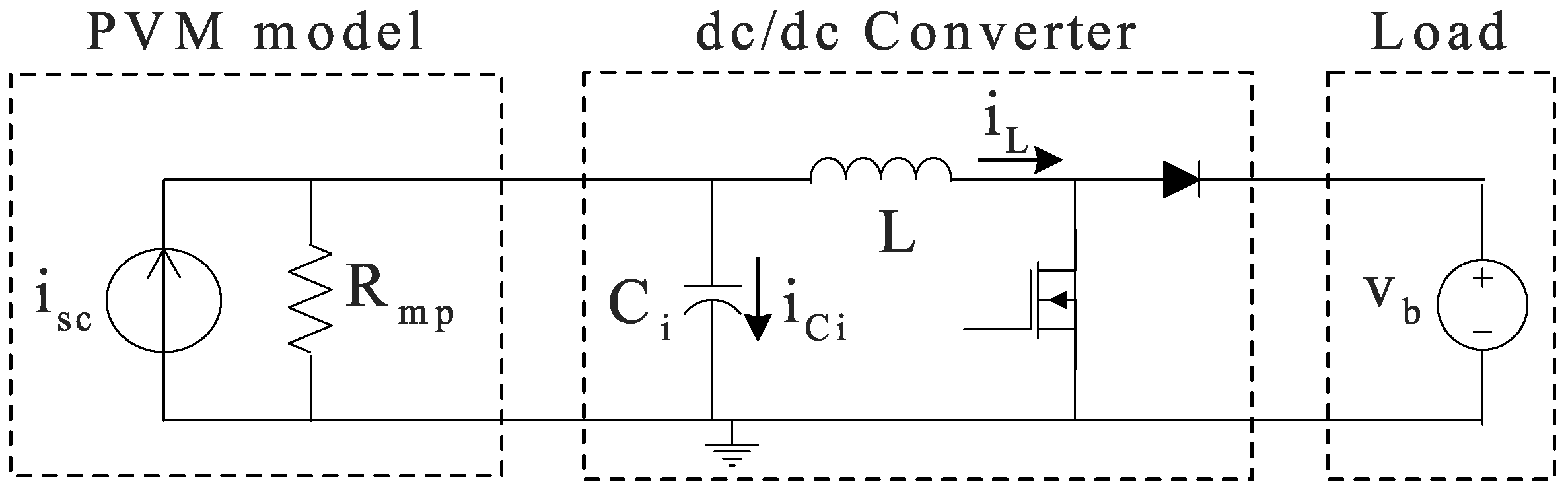
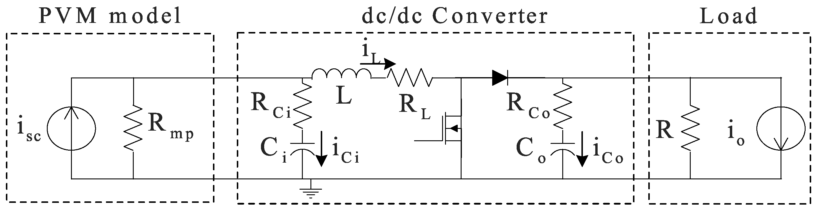
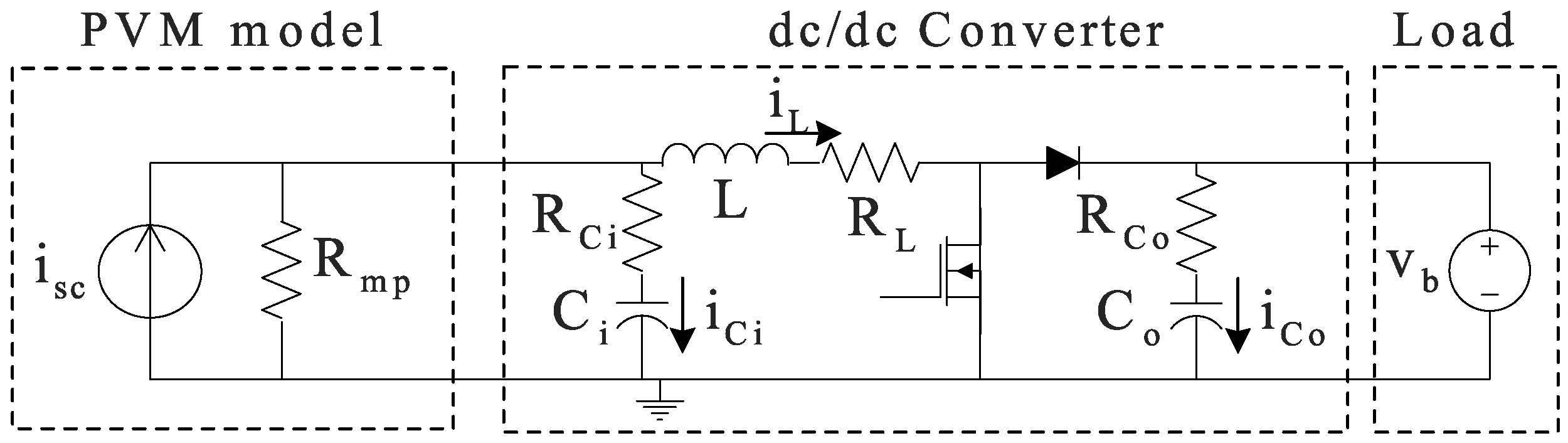
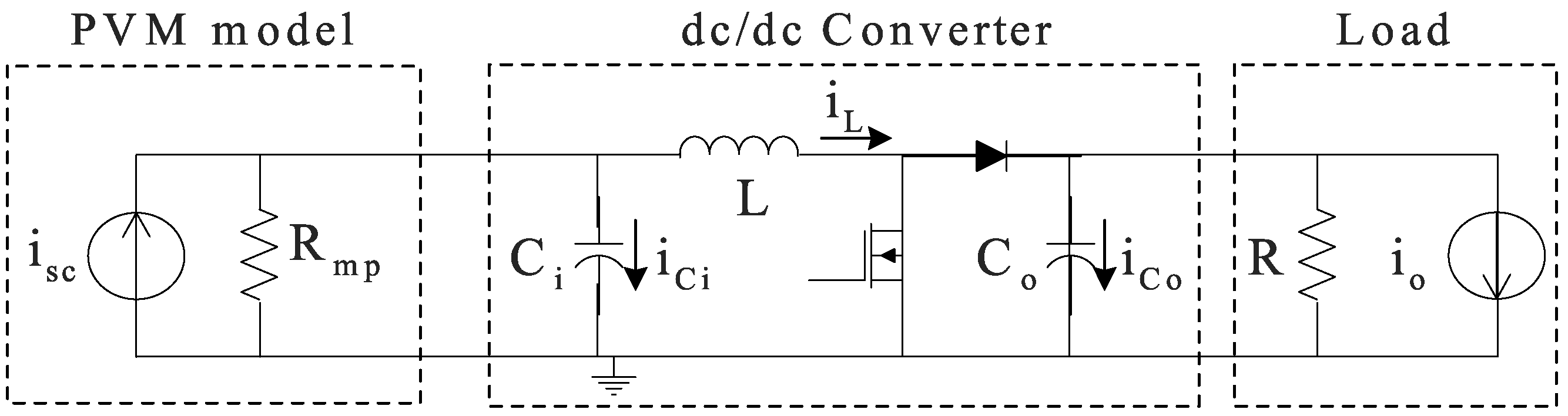
5. Application Example

This section illustrates the usefulness of the proposed models by means of an application example. This example considers the bulk voltage source model and takes into account the parasitic losses of the DC/DC converter. The PV system model was parameterized with L = 56 μH, C i = 44 μF, C o = 44 μF, V C i = 33.15 V, V b = 70 V, I s c = 4.7 A, R m p = 81.87 Ω, R L = 0.3 Ω, R C i = 0.17 Ω, R C o = 0.17 Ω, and f s w = 100 kHz. Then, the equilibrium point has been found by solving (14)–(16).
A PID controller, acting directly on the DC/DC converter duty cycle, has been designed to regulate the PVM voltage since the PV system exhibits minimum phase behavior. In addition, an state observer was designed to validate the observability conditions found in the previous analyses.
The PVM voltage controller was designed by means of the root-locus technique, adopting the following design specifications: damping factor equal to 0.707 and a 20 kHz closed loop bandwidth. Those conditions ensure both the satisfactory dynamic response and the model accuracy for the interesting frequency range [36], but any other conditions can be imposed. The designed controller transfer function is given in (58).
G C ( s ) = - 3 . 077 × 10 - 6 s 2 + 3 . 461 × 10 4 s + 5 . 1673 × 10 8 s
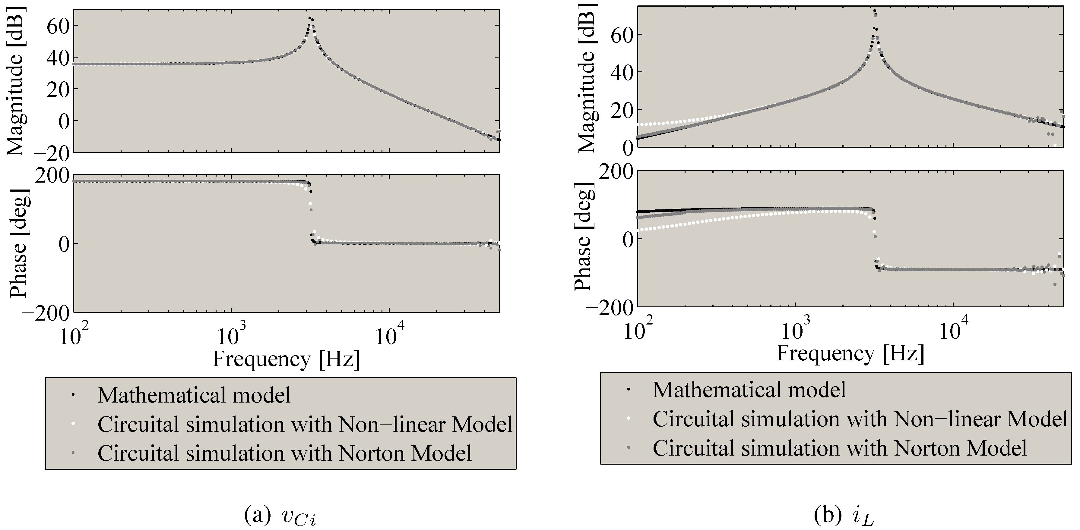
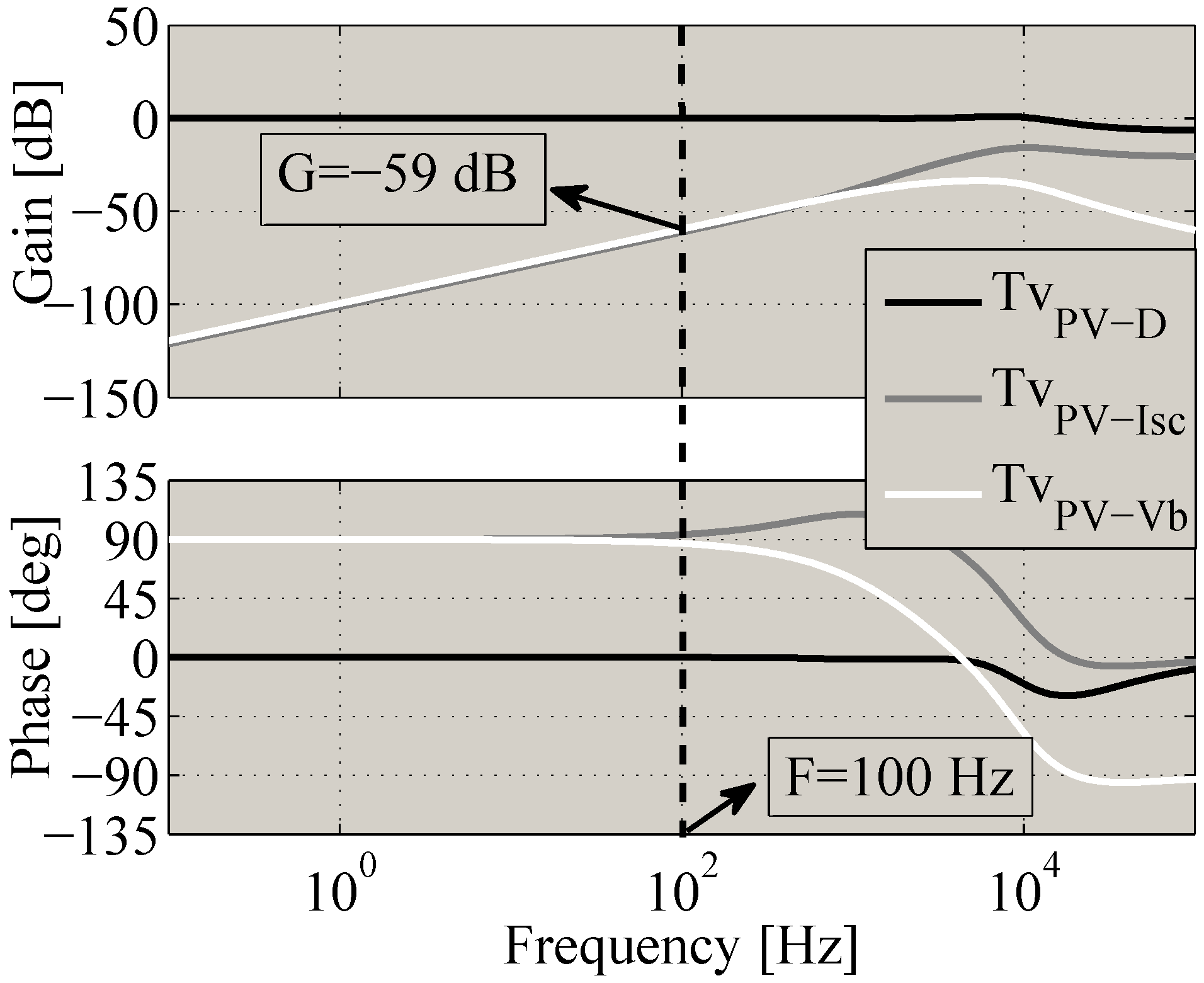
The closed loop transfer functions T v P V - D , T v P V - I s c and T v P V - V b describe the system dynamics for changes on the reference voltage (defined by the MPPT controller), short circuit current (defined by the irradiance), and bulk voltage (defined by the inverter), respectively. The frequency responses of those transfer functions are shown in Figure 14, where a satisfactory reference tracking is observed on T v P V - D , and effective disturbances rejection on T v P V - I s c and T v P V - V b are also exhibited. In particular, considering the connection to a 50 Hz grid, where v b bulk voltage oscillations at 100 Hz are generated, v b perturbations are mitigated by 59 dB. Therefore, less than 0.11% of such 100 Hz oscillations will be transferred to the PVM voltage. Such a condition guarantees a correct MPPT performance with reliable non-electrolytic bulk capacitors, removing the bottleneck classically imposed by the requirement of large bulk capacitances.
The PV system interacting with the designed controller was simulated taking into account the parameters described above and the electrical diagram of Figure 10, in which the Norton PVM model was replaced by the single-diode non-linear model [11] to obtain more realistic results. The simulation considers two BP585 PV panels in series, each of which containing two PVM in series.
Figure 14. Frequency response of the closed loop PV system with G C ( s ) .
Energies 05 01900 g014
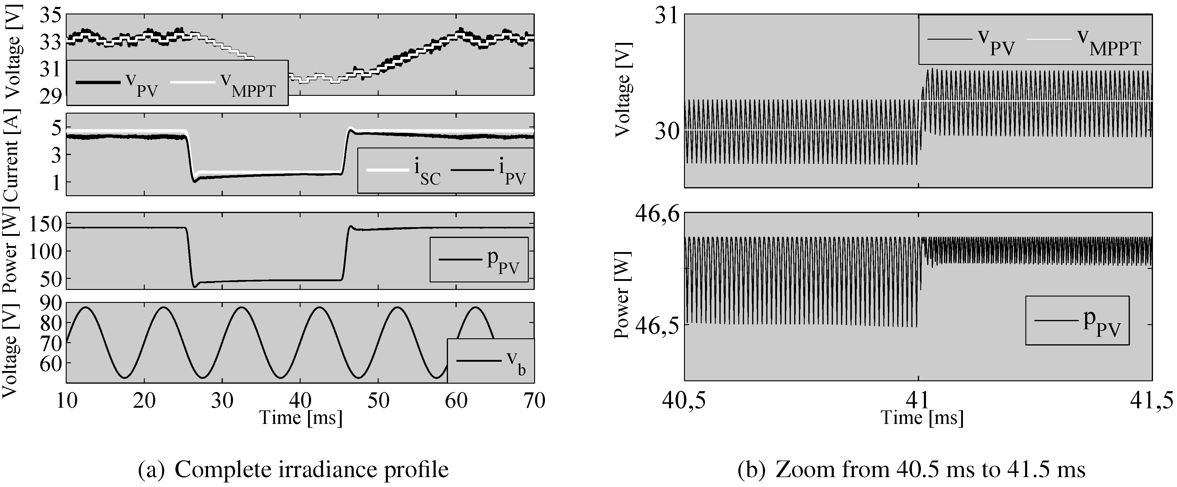
The controller was evaluated by considering an initial irradiance S 1 = 960 W/m 2 , then a step-type disturbance occurs at t = 25 ms reducing the irradiance to S 2 = 560 W/m 2 , returning to S 1 at t = 45 ms. The PV system includes a 44 μF bulk capacitor (non-electrolytic range) that generates a bulk voltage oscillation of 50% of the DC component, which is established by the inverter. Therefore, the designed controller is evaluated with both load and irradiance perturbations. In addition, a P&O MPPT controller designed following [12] was adopted.
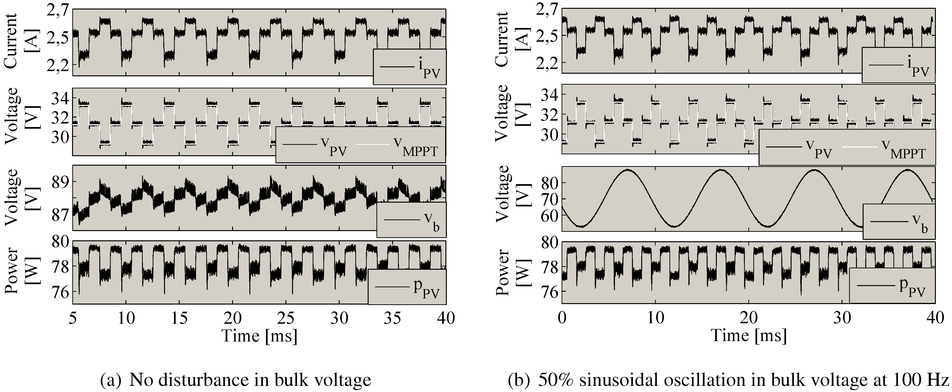
Figure 15(a) shows the simulation of the PV system with the designed controller G C , where a satisfactory tracking of the voltage reference provided by the MPPT controller is observed. Similarly, a satisfactory rejection of both bulk voltage and step irradiance disturbances are achieved. In addition, the correct P&O controller operation is demonstrated by the three-points profile exhibited in the PVM voltage for stable irradiance conditions [6]. Figure 15(b) shows a zoom of the simulation from 40.5 ms to 41.5 ms, where a satisfactory controller performance is observed, providing a stabilization time for the PVM voltage equal to 160 μs. Finally, the system transient response exhibits an oscillation in the power extracted from the PVM lower than 0.1 W, which represents a 0.07% of the maximum power.
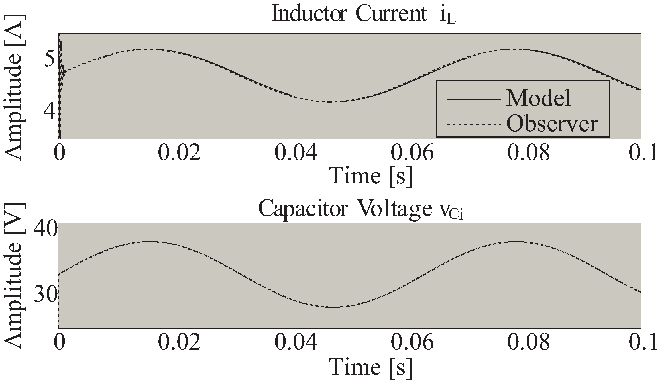
Similarly, the model was used to design complete-order Luenberger observers [37] in two conditions: first, considering the inductor L = 56 μH previously adopted for the transient response simulation, and second, considering the critical inductor L = 2.24 μH calculated from (29) that causes observability loss for the inductor current. In the first case, the numerical observability matrix O b n u m 1 is given in (59), calculated from Equation (28), which exhibits a rank equal to 2, where v C i and i L are observable while v C o is not observable, as reported in Section 3.2. In the second case, the numerical observability matrix O b n u m 2 is given in (60) with a rank equal to 1, where i L is not observable.
O b n u m 1 = - 0 . 16965 0 . 99793 0 - 21210 . 41921 - 3299 . 59903 0 2 . 52718 × 10 8 - 3 . 77059 × 10 8 0
O b n u m 2 = - 0 . 16965 0 . 99793 0 12872 . 46632 - 75719 . 54208 0 - 9 . 76732 × 10 8 5 . 74541 × 10 9 0
Figure 15. PV system transient response by adopting controller G C .
Energies 05 01900 g015
Both observers were simulated using Matlab interacting with PSIM through the Simcoupler toolbox. Figure 16 shows the accurate observer behavior at L = 56 μH condition, where both v C i and i L small-signal behaviors are accurately observed. Instead, the observer designed adopting the inductor calculated from (29) makes i L not observable, as established by (60), and predicted in Section 3.2.
It must be pointed out that the observer previously designed is not suitable to estimate the PV current since small-signal variations are observed only, while the PV current is composed by both the small-signal variations and the large signal component. The main objective of the designed observer is to illustrate the potentiality of the state-space model in the design of more robust and complete observers, e.g., sliding-mode observers and Kalman filters, which could be used to estimate the PV current.
Figure 16. Simulation of the observer designed for L = 56 μH.
Energies 05 01900 g016

6. Experimental Results

The applicability of the proposed modeling approach to real cases was demonstrated by experimentally validating the application example previously presented. The tests were performed using a laboratory prototype with the same parameters considered in the simulations, including the designed G C controller. In addition, a bulk voltage composed by both DC and 100 Hz components was adopted to put in evidence the system capability to operate with small non-electrolytic capacitors. It is noted that this proof-of-concept experiment follows the European 50 Hz grid conditions, but the solution will be also effective in American 60 Hz grid environments.
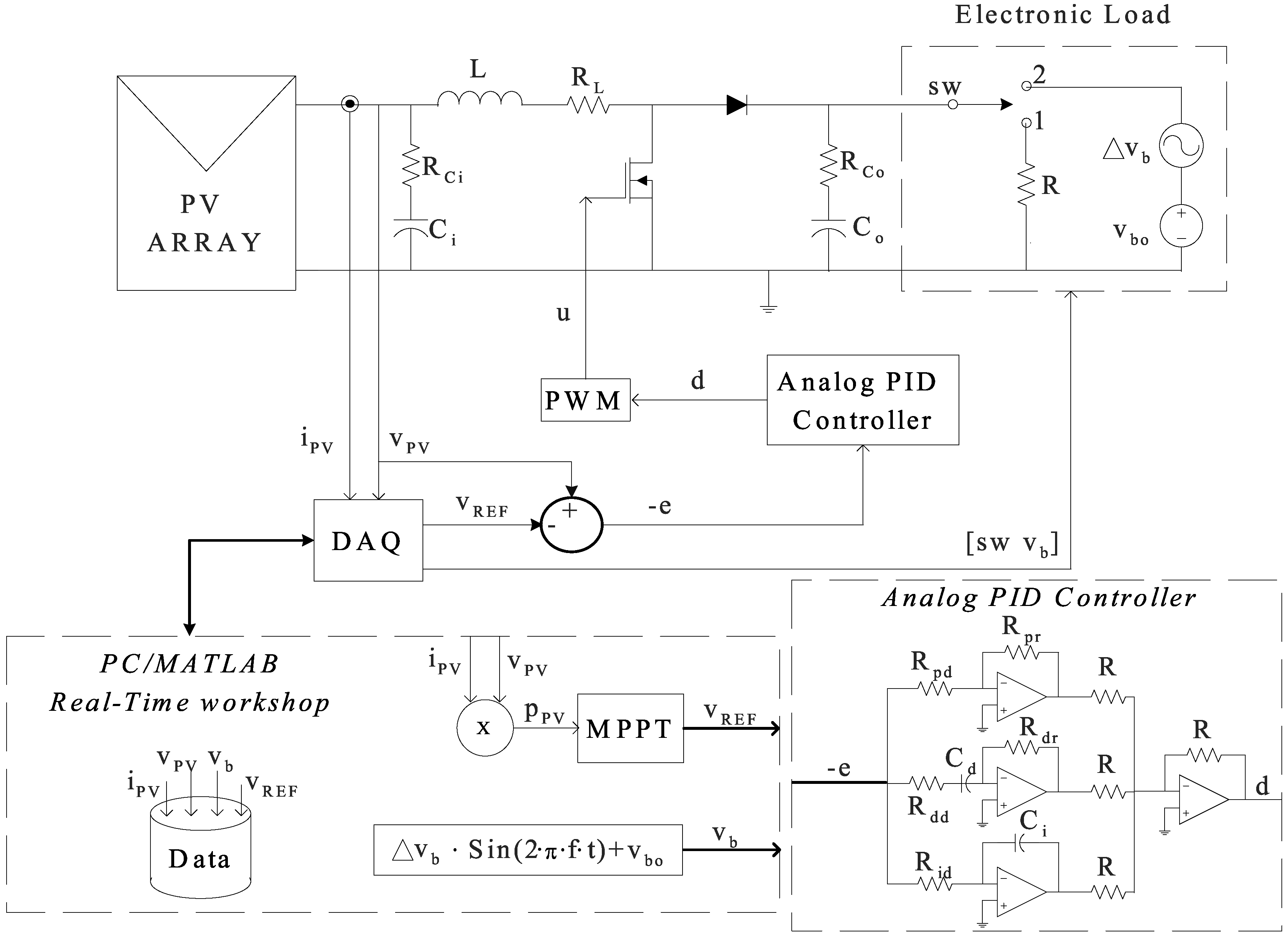
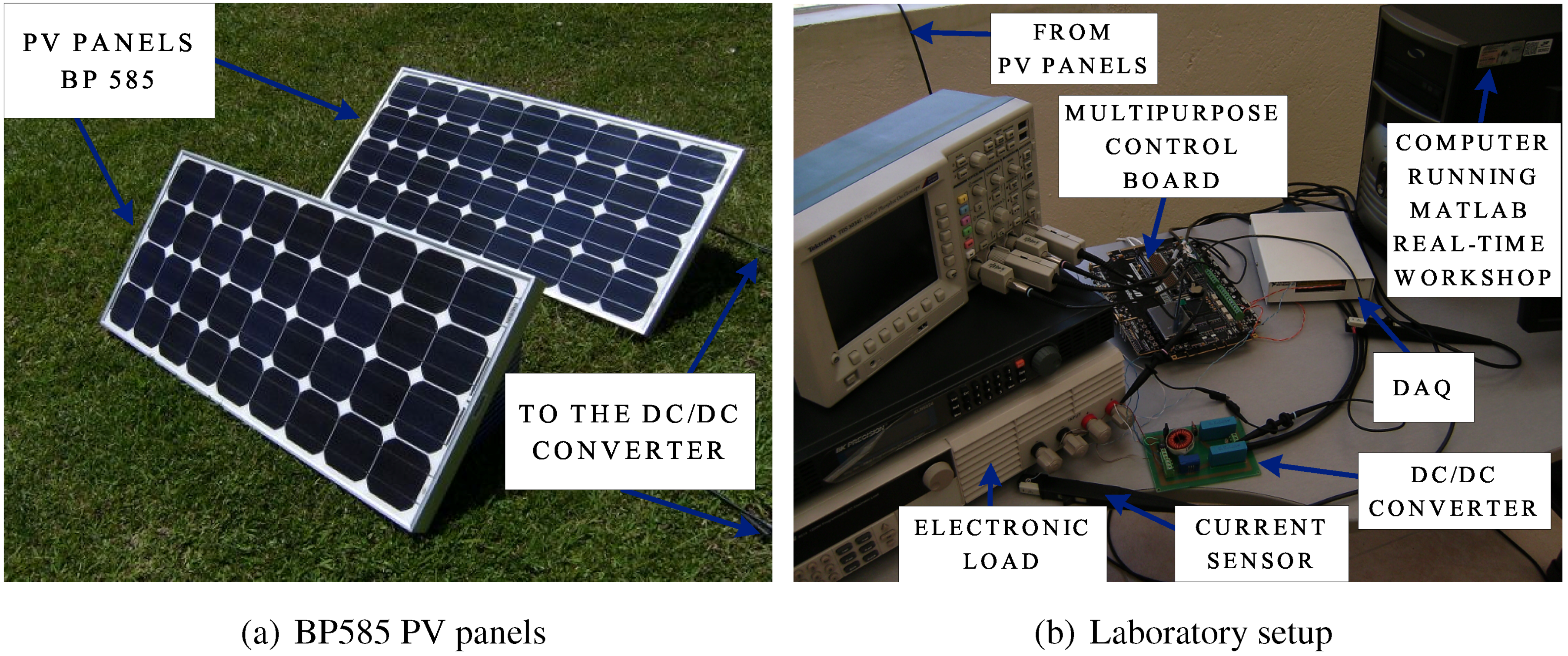
The block diagram of the experimental setup is shown in Figure 17, which outlines the connection of the controlled DC/DC boost converter, the PV array composed by two BP585 PV panels in series, and the load. The controller was implemented using a multipurpose control board with analog PID modules, where an additional pole was introduced [38] to limit the high frequency gain [39], which prevents the noise amplification. Following traditional guidelines [38,39], such a pole was placed at 10 times the dominant poles frequency to reduce its effect on the closed loop behavior (dominant poles at 1.73 × 10⁴ rad/s, additional pole at 1.73 × 10⁵ rad/s). Moreover, the P&O MPPT controller was implemented by using the Matlab Real-Time toolbox and a data acquisition system (DAQ).
An electronic load was used to test the system under two conditions: the first test considers the electronic load operating as a constant resistance R = 100 Ω (switch SW in position 1) to evaluate the operation of the MPPT controller in standard conditions, and to verify the controller’s satisfactory performance by tracking the voltage reference without additional disturbances. The second test considers a small bulk capacitor condition emulated by the electronic load imposing a 100 Hz sinusoidal oscillation with 35 V amplitude superimposed to a DC voltage of 70 V. Such a bulk voltage oscillation corresponds to a 50% perturbation, which is within the non-electrolytic bulk capacitor conditions because typical electrolytic capacitors, in grid connected PV systems, cause bulk voltage oscillations between 1% and 2% of the DC component. This test was performed by configuring the electronic load as a voltage source (switch SW in position 2), whose voltage waveform was imposed by means of a sinusoidal generator implemented into Matlab. In both tests the PV array voltage V P V and current I P V , bulk voltage V b , and MPPT controller output V M P P T were collected. Figure 18(a) and Figure 18(b) show the BP585 PV panels and the laboratory setup used in the experiments, respectively.
Figure 19(a) presents the results from the first test, where the desired performance of the PV voltage controller, following the MPPT voltage reference, is demonstrated. This test also shows that, in the given irradiance conditions, the MPP provides a maximum PV power of 79.3 W. Since such a power corresponds to almost the half of the PV array nominal power (170 W), it is concluded that the irradiance available in the experiments was approximately 470 W/m 2 .
Figure 19(b) depicts the results obtained from the second test, where the analytically predicted behavior of the PV voltage controller following the MPPT voltage reference is validated. The accurate PV voltage regulation is observed in non-electrolytic bulk capacitor conditions that generate large bulk voltage oscillations, 50% at 100 Hz in this case, while the MPPT controller still operates in a stable profile. In this second test the maximum PV power generated was similar to the one obtained in the first test. This condition was achieved by performing the tests in a clear day, and controlling the electronic load to switch from constant resistance (first test) to voltage source (second test) operation almost instantaneously. This procedure guarantees similar irradiance and ambient temperature conditions for both experiments.
Figure 17. Implementation scheme for the experimental tests.
Energies 05 01900 g017
Figure 18. Experimental test bench.
Energies 05 01900 g018
Finally, the achieved PV power profiles make evident the satisfactory performance of the designed controller since it effectively rejects the bulk voltage oscillations. Therefore, the usefulness of the proposed model in real applications is evident.
Figure 19. Experimental tests.
Energies 05 01900 g019

7. Conclusions

This paper develops four models for step-up, double-stage, grid-connected photovoltaic power systems oriented to control design. Such models allow to develop control strategies to reject load and irradiance perturbations, which eventually permits an accurate tracking of the MPP. The analyzed systems exhibit minimum phase behaviors, therefore cascade current-voltage controllers typically adopted for boost converters are not required. Instead, direct duty-cycle-to-PVM voltage controllers can be used. In addition, both simulation and experimental results verify the accuracy of linear controllers designed with the proposed models.
The provided observability and controllability analyses are also useful to design observers and to select suitable control strategies for double-stage PV systems. In addition, the conditions where the system observability is lost have been identified, which are characterized by critical values of the passive elements that generate linear dependences in the observability matrix.
Finally, the proposed models can be used to design state observers to replace PVM current sensors, reducing the PV system costs and increasing its reliability. In addition, the models can be further improved by considering representations of the PVM valid for the whole operating range, e.g., single-diode model. Moreover, the modeling approach can be extended to consider the DCM operation of the DC/DC converter, and to adopt interleaved structures that significantly reduces the PVM voltage ripple. Similarly, more complex DC/DC converters, like the SEPIC, CUK or ZETA, can be adopted to provide step-up/down operation, continuous input and output currents, or higher efficiency.

Acknowledgments

This work was supported by the MATyER and AyE research groups of the Instituto Tecnológico Metropolitano, and the GAUNAL research group of the Universidad Nacional de Colombia under the projects MECOVA-WIND and SMART-ALEN.

References

  1. Bellini, A.; Bifaretti, S.; Iacovone, V. Resonant DC-DC converters for photovoltaic energy generation systems. In Proceedings of the International Symposium on Power Electronics, Electrical Drives, Automation and Motion, Ischia, Italy; 2008; pp. 815–820. [Google Scholar]
  2. Petrone, G.; Spagnuolo, G.; Vitelli, M. Analytical model of mismatched photovoltaic fields by means of Lambert W-function. Sol. Energy Mater. Sol. Cells 2007, 91, 1652–1657. [Google Scholar] [CrossRef]
  3. Gow, J.; Manning, C. Development of a photovoltaic array model for use in power-electronics simulation studies. IEE Proc. 1999, 146, 193–200. [Google Scholar] [CrossRef]
  4. Azab, M. Improved circuit model of photovoltaic array. Int. J. Electr. Power Energy Syst. Eng. 2009, 3, 185–188. [Google Scholar]
  5. Bellini, A.; Bifaretti, S.; Iacovone, V.; Cornaro, C. Simplified model of a photovoltaic module. Energia Solare Test Ricerca ESTER Publ. 2009, 1, 1–5. [Google Scholar]
  6. Femia, N.; Petrone, G.; Spagnuolo, G.; Vitelli, M. Optimization of perturb and observe maximum power point tracking method. IEEE Trans. Power Electron. 2005, 20, 963–973. [Google Scholar] [CrossRef]
  7. Gonzalez, D.; Ramos-Paja, C.; Petrone, G. Automated Procedure for Calculating the Controller Parameters in Photovoltaic dc/dc Converters. Int. Rev. Electr. Eng. 2011, 6, 3027–3040. [Google Scholar]
  8. Noroozian, R.; Abedi, M.; Gharehpetian, G.; Hosseini, S. Combined operation of DC isolated distribution and PV systems for supplying unbalanced AC loads. Renew. Energy 2009, 34, 899–908. [Google Scholar] [CrossRef]
  9. Petrone, G.; Ramos-Paja, C. Modeling of photovoltaic fields in mismatched conditions for energy yield evaluations. Electr. Power Syst. Res. 2011, 81, 1003–1013. [Google Scholar] [CrossRef]
  10. Esram, T.; Chapman, P.L. Comparison of Photovoltaic Array Maximum Power Point Tracking Techniques. IEEE Trans. Energy Convers. 2007, 22, 439–449. [Google Scholar] [CrossRef]
  11. Yau, H.T.; Wu, C.H. Comparison of Extremum-Seeking Control Techniques for Maximum Power Point Tracking in Photovoltaic Systems. Energies 2011, 4, 2180–2195. [Google Scholar] [CrossRef]
  12. Femia, N.; Petrone, G.; Spagnuolo, G.; Vitelli, M. A Technique for Improving P&O MPPT Performances of Double-Stage Grid-Connected Photovoltaic Systems. IEEE Trans. Ind. Electron. 2009, 56, 4473–4482. [Google Scholar]
  13. Petrone, G.; Spagnuolo, G.; Teodorescu, R.; Veerachary, M.; Vitelli, M. Reliability Issues in Photovoltaic Power Processing Systems. IEEE Trans. Ind. Electron. 2008, 55, 2569–2580. [Google Scholar] [CrossRef]
  14. Ramos-Paja, C.A.; Perez, E.; Gonzalez-Montoya, D.; Carrejo, C.E.; Simon-Muela, A.; Alonso, C. Modeling of full Photovoltaic Systems Applied to Advanced Control Strategies. In Proceedings of the International Conference on Renewable Energies and Power Quality, Granada, Spain; 2009. [Google Scholar]
  15. Liu, S.; Dougal, R. Dynamic Multiphysics Model for Solar Array. lEEE Trans. Energy Convers. 2002, 17, 285–294. [Google Scholar]
  16. Femia, N.; Petrone, G.; Spagnuolo, G.; Vitelli, M. A new analog MPPT technique: TEODI. Prog. Photovolt. Res. Appl. 2010, 18, 28–41. [Google Scholar] [CrossRef]
  17. Chenni, R.; Zarour, L.; Amarouayache, M.; Bouzid, A. A New Design for Analogue Maximum Power Point Tracking. Int. Rev. Electr. Eng. 2008, 3, 93–99. [Google Scholar]
  18. Spagnuolo, G.; Petrone, G.; Vitelli, M.; Calvente, J.; Ramos-Paja, C.; Giral, R.; Mamarelis, E.; Bianconi, E. A fast current-based MPPT technique employing sliding mode control. IEEE Trans. Ind. Electron. 2012, 99, 1–11. [Google Scholar] [CrossRef]
  19. Vitelli, M.; Petrone, G.; Spagnuolo, G. An analog technique for Distributed MPPT PV applications. IEEE Trans. Ind. Electron. 2011, 99, 1–10. [Google Scholar] [CrossRef]
  20. Erickson, R.; Maksimovic, D. Fundamentals of Power Electronics; Kluwer Academic Publishers: New York, NY, USA, 2004. [Google Scholar]
  21. Ramos-Paja, C.; Gonzalez, D.; Carrejo, C. Predictive control of a photovoltaic dc/dc converter. In Proceedings of the 6th IET International Conference on Power Electronics, Machines and Drives (PEMD2012), Bristol, UK; 2012; pp. 1–6. [Google Scholar]
  22. Luo, P.; Ming, X.; Zhang, B.; Li, Z.J. Analysis of the Stability and Ripple of PSM Converter in DCM by EB Model. In Proceedings of the International Conference on Communications, Circuits and Systems, (ICCCAS), Fukuoka, Japan; 2007; pp. 1240–1243. [Google Scholar]
  23. El Aroudi, A.; Alarcon, E.; Rodriguez, E.; Leyva, R.; Villar, G.; Guinjoan, F.; Poveda, A. Ripple Based Index for Predicting Fast-Scale Instability of DC-DC Converters in CCM and DCM. In Proceedings of the IEEE International Conference on Industrial Technology (ICIT), Mumbai, India; 2006; pp. 1949–1953. [Google Scholar]
  24. Aranda, E.; Galan, J.; de Cardona, M.; Marquez, J. Measuring the I-V curve of PV generators. IEEE Ind. Electron. Mag. 2009, 3, 4–14. [Google Scholar] [CrossRef]
  25. Giral, R.; Carrejo, C.; Vermeersh, M.; Saavedra-Montes, A.; Ramos-Paja, C. PV field distributed maximum power point tracking by means of an active bypass converter. In Proceedings of the International Conference on Clean Electrical Power (ICCEP), Ischia, Italy; 2011; pp. 94–98. [Google Scholar]
  26. Nousiainen, L.; Puukko, J.; Suntio, T. Appearance of a RHP-zero in VSI-based photovoltaic converter control dynamics. In Proceedings of the IEEE 33rd International Telecommunications Energy Conference (INTELEC), Amsterdam, The Netherlands; 2011; pp. 1–8. [Google Scholar]
  27. Hoagg, J.; Bernstein, D. Nonminimum-phase zeros—much to do about nothing—classical control—revisited part II. IEEE Control Syst. 2007, 27, 45–57. [Google Scholar] [CrossRef]
  28. Jeong, G.J.; Kim, I.H.; Son, Y.I. Application of simple adaptive control to a DC/DC boost converter with load variation. In Proceedings of ICROS-SICE International Joint Conference, Fukuoka, Japan; 2009; pp. 1747–1751. [Google Scholar]
  29. Muhida, R.; Park, M.; Dakkak, M.; Matsuura, K.; Tsuyoshi, A.; Michira, M. A maximum power point tracking for photovoltaic-SPE system using a maximum current controller. Sol. Energy Mater. Sol. Cells 2003, 75, 697–706. [Google Scholar] [CrossRef]
  30. Suntio, T.; Leppaaho, J.; Huusari, J.; Nousiainen, L. Issues on Solar-Generator Interfacing With Current-Fed MPP-Tracking Converters. IEEE Trans. Power Electron. 2010, 25, 2409–2419. [Google Scholar] [CrossRef]
  31. Louganski, K.P.; Lai, J.S. Current Phase Lead Compensation in Single-Phase PFC Boost Converters With a Reduced Switching Frequency to Line Frequency Ratio. IEEE Trans. Power Electron. 2007, 22, 113–119. [Google Scholar] [CrossRef]
  32. Boulter, B. Applying drive performance specifications to systems applications. I. Speed performance. IEEE Trans. Ind. Appl. 2001, 37, 1082–1087. [Google Scholar] [CrossRef]
  33. Donoghue, S.; Finch, J.; Giaouris, D.; Jones, A. Generalized Minimum Variance Controller as a Velocity Loop Controller of a Casting Drum Drive in a Polyester Manufacturing Line. In Proceedings of the World Congress on Engineering 2008 (WCE 2008), London, UK; 2008; Volume 3, pp. 1–6. [Google Scholar]
  34. Saloux, E.; Teyssedou, A.; Sorin, M. Explicit model of photovoltaic panels to determine voltages and currents at the maximum power point. Sol. Energy 2011, 85, 713–722. [Google Scholar] [CrossRef]
  35. Leppaaho, J.; Suntio, T. Dynamic properties of PCM-controlled current-fed boost converter in photovoltaic system interfacing. In Proceedings of the 14th European Conference on Power Electronics and Applications (EPE 2011), Birmingham, UK; 2011; pp. 1–10. [Google Scholar]
  36. Vidal-Idiarte, E.; Martinez-Salamero, L.; Calvente, J.; Romero, A. An Control Strategy for Switching Converters in Sliding-Mode Current Control. IEEE Trans. Power Electron. 2006, 21, 553–556. [Google Scholar] [CrossRef]
  37. Chen, C. Linear System Theory and Design; Oxford University Press: New York, NY, USA, 1999. [Google Scholar]
  38. Kristiansson, B.; Lennartson, B. Robust and optimal tuning of PI and PID controllers. IEE Proc. Control Theory Appl. 2002, 149, 17–25. [Google Scholar] [CrossRef]
  39. Kristiansson, B.; Lennartson, B. Robust tuning of PI and PID controllers: Using derivative action despite sensor noise. IEEE Control Syst. 2006, 26, 55–69. [Google Scholar] [CrossRef]

