Article

Analysis and Design of Independent DC Bus Structure Multiport Power Electronic Transformer Based on Maximum Power Transmission Capability of Low-Voltage DC Ports

1
School of Electrical Engineering, Beijing Jiaotong University, Beijing 100044, China
2
College of Automation, Chongqing University of Posts and Telecommunications, Chongqing 400065, China
*
Author to whom correspondence should be addressed.
Energies 2024, 17(5), 1096; https://doi.org/10.3390/en17051096
Submission received: 11 January 2024 / Revised: 21 February 2024 / Accepted: 22 February 2024 / Published: 25 February 2024
(This article belongs to the Special Issue High-Power Electronics in Distribution Grids)

Abstract

:
Owing to the diverse connection configurations of dual active bridge converters, a multiplicity of low-voltage DC port structures are anticipated to emerge in the independent DC bus structure multiport power electronic transformer (IDBS-MPET). An inadequate low-voltage DC port structure exacerbates the power imbalance in IDBS-MPET, presenting a risk of overmodulation even when transmitting relatively low levels of power. To overcome this limitation, a design scheme of IDBS-MPET topology based on the maximum power transmission capability of the low-voltage DC ports is proposed in this paper. Three topology design rules are derived from the maximum power transmission capability results of more than 80 typical IDBS-MPET topologies. The symmetrical triple cross-phase connection structure, the symmetrical double cross-phase connection structure and the single-phase connection structure are sequentially identified as the three most optimal structures of low-voltage DC ports. By employing the proposed design methodology, each low-voltage DC port achieves its maximum power transfer capability relative to other configurations. The effectiveness of the proposed design scheme is validated by an optimal designed IDBS-MPET topology with six low-voltage DC ports.

1. Introduction

A multiport power electronic transformer (MPET) provides a competitive solution for the networking of hybrid AC/DC distribution systems due to its compatibility and advanced functionalities [1,2]. Most of the existing MPETs provide at least a medium-voltage AC port, a low-voltage AC port and a low-voltage DC port [3]. The medium-voltage AC port is indispensable for absorbing the active power from the AC grid to feed the next stage [4]. Generally, three-phase cascaded H-bridge (CHB) converters are adopted to form the medium-voltage AC port [5,6,7]. The low-voltage AC port provides the interfaces to conventional AC loads. Nevertheless, compared to the MPET, the conventional line frequency transformer exhibits superior performance in terms of cost-effectiveness, robustness and reliability when supplying power to conventional AC loads.
Due to the massive growth of DC resources and DC loads in the distribution network, the demand for low-voltage DC (LVDC) ports on the MPET significantly surpasses that for the low-voltage AC ports. The LVDC ports provide efficient integration of distributed generation (DG), electric vehicle (EV) charging stations, energy storage systems (ESS), data centers and other industrial DC loads [8,9]. Since the nominal voltage of DGs and DC loads are different, an MPET with multiple LVDC ports is significantly necessary. Multiple LVDC ports provide interfaces with multiple voltage levels and power levels. DGs and linear/nonlinear DC loads can be connected to different LVDC ports, avoiding adverse interactions of direct electrical coupling.
Generally, isolated bidirectional DC-DC converters, such as dual active bridge (DAB) converters, are adopted in MPETs to produce LVDC links on each of their output terminals [10,11]. For the most part, all of the LVDC links are paralleled together to form a common DC bus, and thus only one LVDC port of single voltage level is provided [12,13,14]. In the later stage of the common DC bus, additional DC/DC converters are needed to meet the access requirements of DGs and DC loads of different voltage levels. These additional DC/DC converters increase the hardware cost and reduce the system efficiency.
In [15], a five-terminal hybrid AC/DC microgrid with four LVDC ports was proposed. The topology of the microgrid is the same as that of the MPET. Multiple LVDC ports are naturally obtained by separating the common DC bus into four parts without adding any additional converters. Moreover, the LVDC ports are electrically isolated from each other and each of them can be protected from the faults of the other ones. Based on the topology proposed in [15], the independent DC bus structure multiport power electronic transformer (IDBS-MPET) can be constructed. The output voltage of DABs can be controlled to meet the requirements of multiple voltage levels. The parallel quantities of DABs can be configured to meet the requirements of multiple power levels. Compared with the common DC bus structure multiport power electronic transformer (CDBS-MPET), a huge number of power semiconductor devices have been saved in the IDBS-MPET. Since the high-frequency transformer is applied in the DAB, each LVDC port is galvanically isolated from the others.
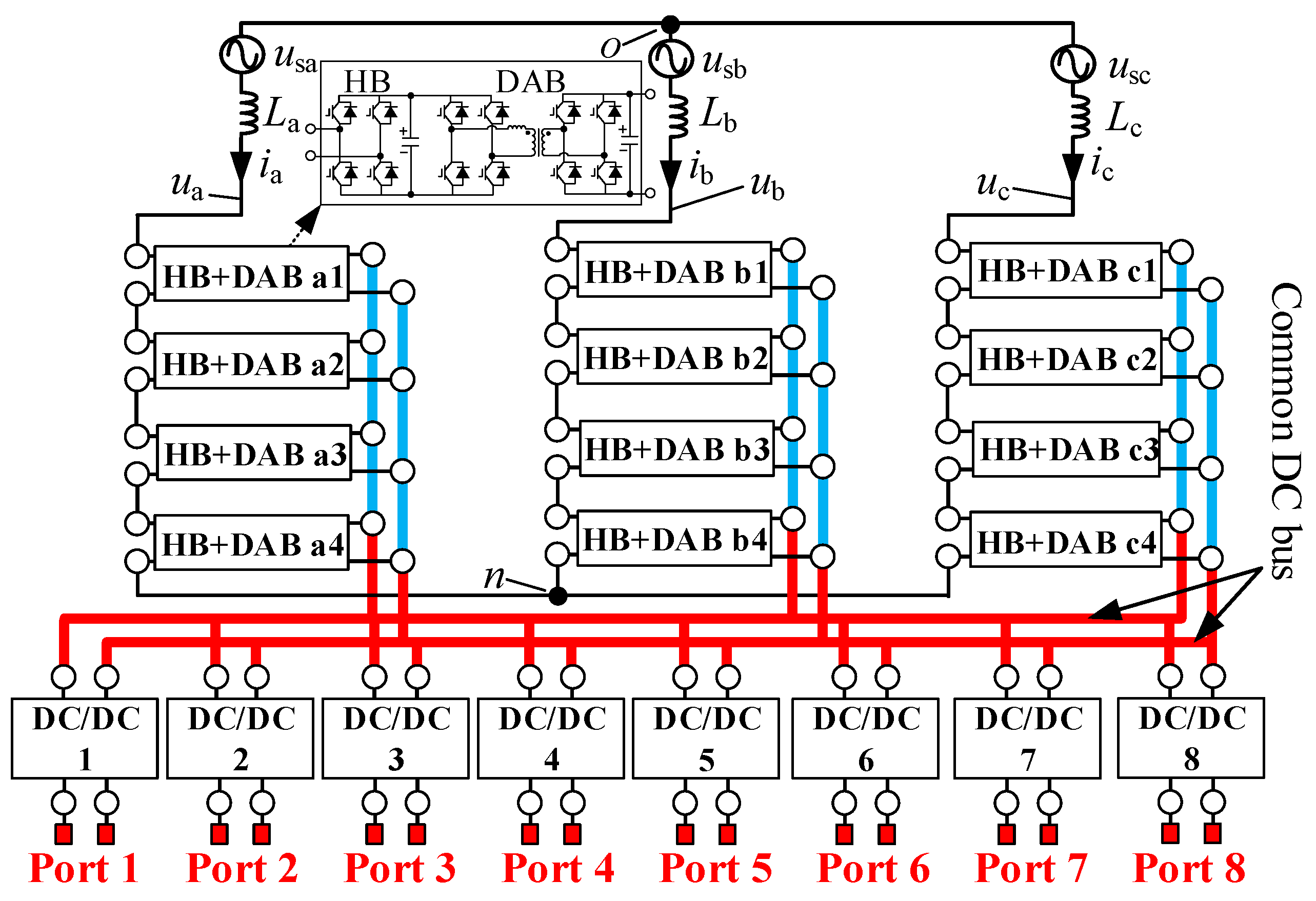
A typical IDBS-MPET is shown in Figure 1. The DAB features a multitude of output terminal connection methodologies. A diversity of parallel connection configurations for DAB output terminals can be identified. Port 1 consists of three DABs from three different phases. Port 2 comprises one DAB from a single phase. Port 6 involves DABs from two separate phases. The term ‘phase’ in this paper refers to the AC grid phases a, b or c. If the LVDC port is composed of paralleled DABs from two or three phases, it is called the cross-phase connection port (see Section 2). In addition, in a cross-phase connection port, the quantities of DABs distributed in each phase will be different. Therefore, DGs or DC loads of a cross-phase connection port will be distributed in two phases or three phases, and evenly or unevenly.
Indeed, the cross-phase-connected converters may have a positive impact on the power balancing of loads. In [16,17], a full-range power auto-balance PET is proposed. Each input-stage-side dc link is connected in parallel to three isolation- and output-stage cascaded converter chains. The three converter chains are cross-phase connected to three output phases. In the construction of DC ports by the auto-balance PET, additional DC/DC converters are still required; however, this is not the case with the IDBS-MPET. The IDBS-MPET can flexibly and conveniently offer multiple isolated LVDC ports, which presents a significant advantage in future-oriented distribution network scenarios where DC loads are increasingly predominant. In [18,19], a multilevel converter with three AC ports (i.e., AC Port 1~3) is proposed. To avoid power imbalance, H-bridge converters in AC Port 1 are connected to one of the phases either in AC Port 2 or AC Port 3 through DABs. However, the influence of the cross-phase connection patterns of converters on the MPET’s ability to deal with power imbalance has not been quantitatively analyzed. The design scheme of the cross-phase connection patterns of converters has not been studied. In the PET discussed in references [18,19], only AC ports are provided, with no provision for DC ports. In contrast, the IDBS-MPET employs a more flexible cross-phase connection approach. When constructing LVDC ports, parallel connection methods for DAB outputs allows for a more flexible distribution of loads across one, two or three phases.
In this paper, a systematic analysis and design scheme of IDBS-MPET is proposed. The main technical contributions of this paper are summarized as follows:
(1)
Three basic structures of LVDC ports are established and all of the IDBS-MPET topologies can be derived based on them. Accordingly, the general graphical representation and naming method of the IDBS-MPET are given.
(2)
The maximum power transmission capability (MPTC) is proposed to evaluate the capability of the IDBS-MPET to deal with a power imbalance.
(3)
Three topology design rules are derived from the MPTC calculation results of more than 80 typical IDBS-MPET topologies. Based on the three topology design rules, the systematic design scheme of the IDBS-MPET topology is proposed. The optimal IDBS-MPET to deal with a power imbalance can be found quickly and easily.
The rest of this article is organized as follows. Section 2 introduces the topology configuration of the IDBS-MPET. In Section 3, the definition and calculation method of MPTC is proposed. In Section 4, three topology design rules and the systematic design scheme of the IDBS-MPET topology is proposed. In Section 5, the IDBS-MPET with six LVDC ports is designed to validate the effectiveness of the proposed design scheme. Section 6 provides a discussion. Finally, the conclusion is drawn in Section 7.

2. Topology Configuration of the IDBS-MPET

This section is composed of three parts. First, an overview of the IDBS-MPET is provided. Second, three basic structures of LVDC ports are established based on the parallel connection patterns of DAB output terminals. Third, a comprehensive graphical depiction and nomenclature approach for the IDBS-MPET are provided.

2.1. Overview of IDBS-MPET

The IDBS-MPET features a comprehensive multiport topology that effectively integrates H-bridge converters and DAB converters to form multiple LVDC ports. The topology is characterized by its three-phase input, with each phase hosting a series of H-bridges coupled to corresponding DABs. These DABs are connected in parallel, which directly yields the LVDC ports (Port 1 to Port 8) without the need for additional DC/DC converters.
As is shown in Figure 1, Port 2, 3, 4 and 5 consist of one DAB from a single phase. Port 8 consists of two DABs from a single phase. The green striped lines are used to indicate the single-phase connection wires. The LVDC port can be formed by the parallel connection of DABs from two phases, such as Port 6 and 7. Since Port 7 consists of four DABs, it will have the power supply ability for the higher power DC load. The red solid lines are used to indicate the cross-phase connection wires. The LVDC port can be formed by the parallel connection of DABs from three phases, such as Port 1. Port 1 consists of three DABs from phases a, b and c, respectively.
The properties of the IDBS-MPET can be expressed as follows:
(1)
Lower hardware costs. Without adding any additional DC/DC converters, multiple LVDC ports are directly formed by the parallel connection of DABs. Therefore, a huge amount of power semiconductors in the IDBS-MPET can be saved compared with the CDBS-MPET.
(2)
Cross-phase connections are adopted. As multiple LVDC ports are distributed in three phases independently, a power imbalance will arise. To better deal with the problem, the cross-phase connection patterns of DABs are adopted in the IDBS-MPET.
(3)
Galvanic isolation. Since there is a high-frequency transformer in each DAB, all of the LVDC ports are galvanically isolated from each other and from the gird as well.
(4)
Modularity design. All H-bridges have the same electrical parameters, and so do all DABs. The power level of the entire power electronic transformer can be improved only by expanding the number of modules.
The control techniques employed in the IDBS-MPET include the management of grid current and DC capacitor voltage in the CHB [15], voltage feedback control in the DAB [20], maximum power point control in the photovoltaic (PV) inverter [21], and charging control in EVs and ESS [22,23]. Common-duty-ratio control can be employed for paralleled DABs [24].
In order to quantify the reduction in hardware costs of the IDBS-MPET, a typical application scenario is constructed. In this application scenario, the topology of the IDBS-MPET is shown in Figure 1 and the topology of the CDBS-MPET is shown in Figure 2.
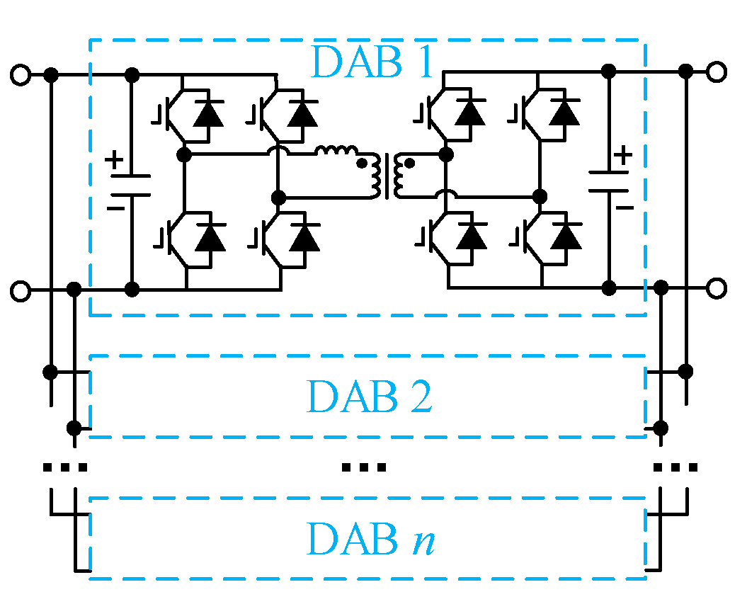
Both MPETs have eight LVDC ports (i.e., Port 1 to 8) and the devices connected to Port 1 to 8 are listed in Table 1. The circuit parameters of the H-bridges and DABs in the two MPETs are the same and they are listed in Table 2. Moreover, the additional DC/DC converters (i.e., DC/DC 1 to 8) are needed in the CDBS-MPET to construct eight mutual galvanically isolated LVDC ports of different power levels and voltage levels. As shown in Figure 3, in order to meet the power level requirements, the input-parallel output-parallel (IPOP) DABs are used to construct DC/DC 1 to 8. The n in Figure 3 indicates the amount of IPOP DABs and their specific values are shown in Table 3.
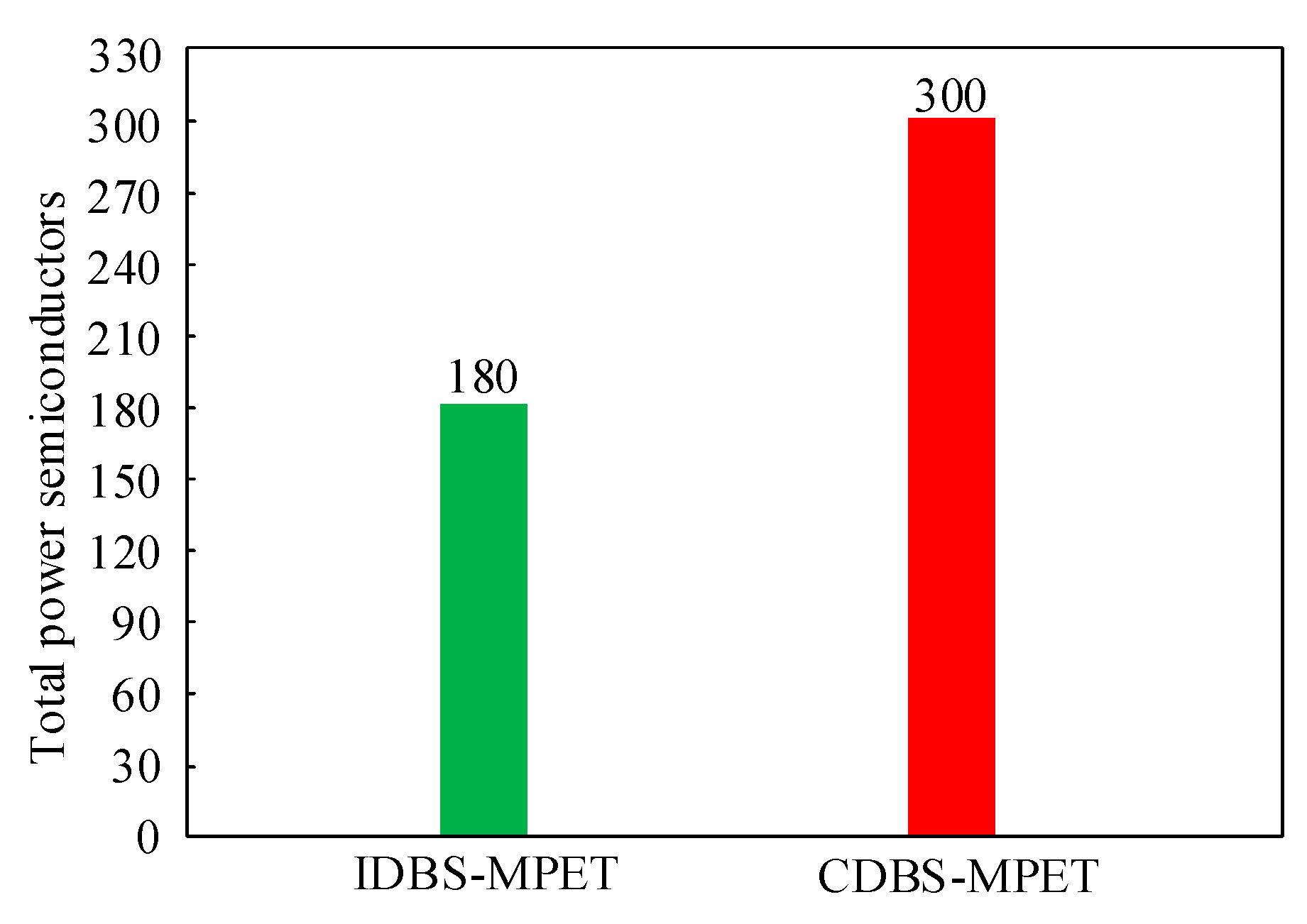
The total power semiconductors in the IDBS-MPET and CDBS-MPET are shown in Figure 4. There are 180 power semiconductors in total used in the H-bridges and DABs of the IDBS-MPET. There are 300 power semiconductors in total used in the H-bridges, DABs and DC/DC 1 to 8 of the CDBS-MPET. In the same application scenario, the IDBS-MPET has reduced the hardware cost of power semiconductors by 40%.

2.2. Basic Structure of LVDC Ports

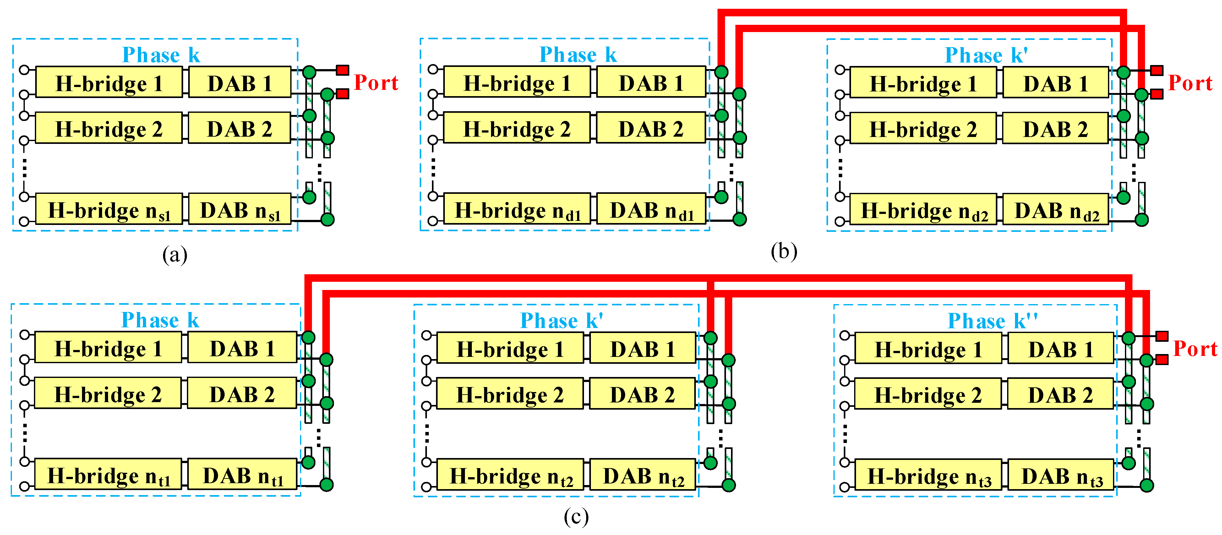
Based on the connection patterns of DAB output terminals, three basic structures of LVDC ports are established. All kinds of IDBS-MPETs can be derived from the combination of the three basic structures. As is shown in Figure 5, they are the single-phase connection port (S-Port), the double cross-phase connection port (D-Port) and the triple cross-phase connection port (T-Port). In Figure 5, k, k′ and k″ all denote the grid phase a, b or c, whereas k ≠ k′ ≠ k″.
The S-Port consists of ns1 DABs from phase k. As shown in Figure 1, Port 2, Port 3, Port 4, Port 5 and Port 8 belong to the category S-Port. The DGs and DC loads connected to the S-Port are distributed in one phase. The D-Port consists of nd1 DABs from phase k and nd2 DABs from phase k′. The DGs and DC loads connected to the D-Port are distributed in two phases, evenly or unevenly. If nd1 = nd2, the D-Port is denoted as a symmetrical D-Port; otherwise, it is denoted as an asymmetrical D-Port. As shown in Figure 1, Port 6 and Port 7 belong to the category D-Port and both of them are symmetrical D-Ports. The T-Port consists of nt1 DABs from phase k, nt2 DABs from phase k′ and nt3 DABs from phase k″. The DGs and DC loads connected to the T-Port are distributed in three phases, evenly or unevenly. If nt1 = nt2 = nt3, the T-Port is denoted as a symmetrical T-Port; otherwise, it is denoted as an asymmetrical T-Port. As shown in Figure 1, Port 1 belongs to the category T-Port and it is a symmetrical T-Port.

2.3. Comprehensive Graphical Depiction and Nomenclature Approach for the IDBS-MPET

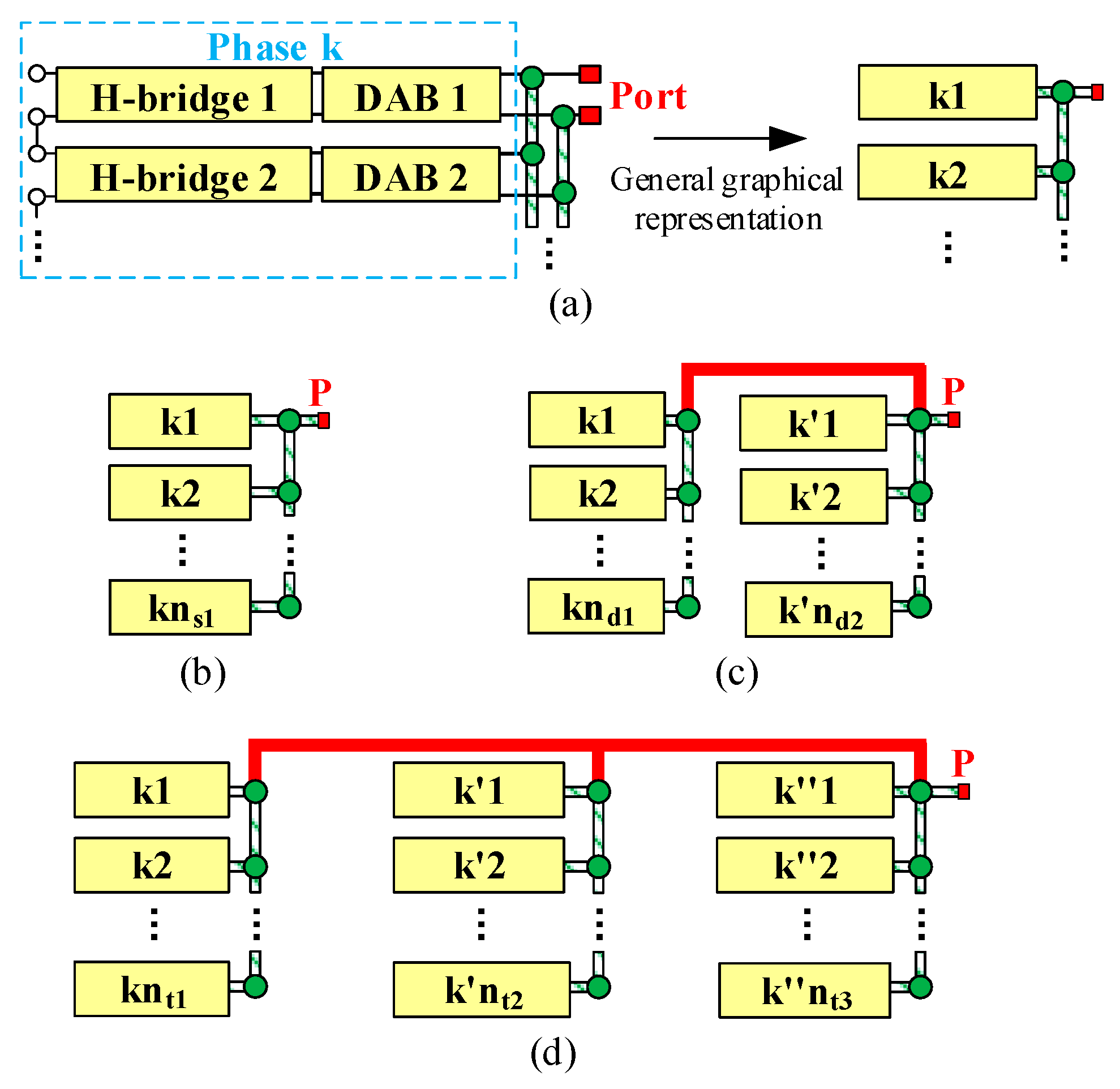
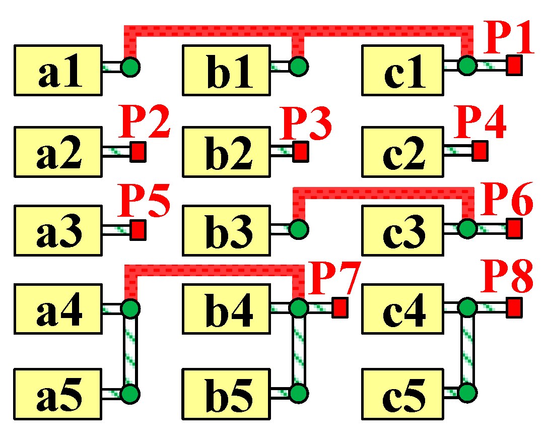
In order to simplify the representation of the IDBS-MPET, a comprehensive graphical depiction and nomenclature approach for the IDBS-MPET are established. The comprehensive graphical depiction and nomenclature of LVDC ports are shown in Figure 6 and Table 4. Each H-bridge and its connected DAB are combined and represented by one block. Port is abbreviated to the letter P. Red solid lines are still used to indicate the cross-phase connection wire and green striped lines are still used to indicate the single-phase connection wire. As is shown in Figure 7, it is the graphical representation of the IDBS-MPET in Figure 1.
The S-Port is named as S(ns)(ns1). This means that there exists ns S-Ports and each of them consists of ns1 DABs. The D-Port is named as D(nd)(nd1, nd2). This means that there exists nd D-Ports and each of them consists of nd1 DABs from phase k and nd2 DABs from phase k′. The T-Port is named as T(nt)(nt1, nt2, nt3). This means that there exists nt T-Ports and each of them consists of nt1 DABs from phase k, nt2 DABs from phase k′ and nt3 DABs from phase k″.
The naming of the whole IDBS-MPET can be obtained by adding another two indicators, namely, the total quantity of H-bridge converters per phase N(NH) and the total quantity of LVDC ports P(NP). The N(NH) indicates that there are in total NH H-bridge converters per phase and the P(NP) indicates that there are NP LVDC ports in total. Thus, the naming of the IDBS-MPET is expressed as follows:
N(NH)P(NP)-S(ns)(ns1)D(nd)(nd1, nd2)T(nt)(nt1,nt2,nt3)
In (1), the N(NH)P(NP) is called the general description part and the S(ns)(ns1)D(nd)(nd1, nd2)T(nt)(nt1,nt2,nt3) is called the LVDC port description part, written in the S, D and T sequence. The S, D and T sequence is not necessarily in one-to-one correspondence with the sequence of port numbers 1, 2, 3 and so on. The purpose of the LVDC port description part is to indicate which kinds and how many of the three basic structures of LVDC ports are used in the IDBS-MPET. In addition, it is worth mentioning that (1) is the standard form of IDBS-MPET naming. If there is more than one kind of S-Port, D-Port or T-Port in the IDBS-MPET, the S(ns)(ns1), D(nd)(nd1, nd2) or T(nt)(nt1,nt2,nt3) will recur more than once in (1). The naming of the IDBS-MPET in Figure 7 will be N(5)P(8)-S(4)(1)S(1)(2)D(1)(1,1)D(1)(2,2)T(1)(1,1,1).

3. MPTC Definition and Calculation Method

Due to the various structures of LVDC ports, the DGs or DC loads of each LVDC port will be distributed in one phase, two phases or three phases, and evenly or unevenly. A power imbalance will arise in the IDBS-MPET among three phases and among H-bridge converters of each phase. When the DGs and DC loads are distributed in three phases extremely unevenly, the power imbalance will become severe, resulting in the instability of the IDBS-MPET. The optimal IDBS-MPET is the one with the maximum capability to deal with a power imbalance. In order to evaluate the capability, the MPTC is proposed in this section. This section is composed of two parts. First, the definition of the MPTC is proposed. Second, the calculation method of the MPTC is proposed.

3.1. MPTC Definition

The MPTC of an LVDC port is calculated under the condition that the IDBS-MPET operates safely and stably. However, the maximum allowable phase voltage of three-phase CHB converters is lower than the sum of the H-bridge converters’ DC voltages in this phase. In addition, the maximum allowable AC voltage of each H-bridge converter is lower than its DC voltage. The over modulation of the IDBS-MPET AC phase voltage and the over modulation of the H-bridge converter AC voltage should be avoided. Thus, the constraints of the modulation ratio are expressed as follows:
k a , b , c , j n 1 , , N H m k 1 m k j n 1
where mk is the modulation ratio of phase k; mkjn is the modulation ratio of the jnth H-bridge in phase k.
Then, the rated power of an LVDC port can be defined. Due to the modular design of the IDBS-MPET, the rated power of all of the DABs is the same. Let PN,DAB be the rated power of one DAB. If Port j consists of nj DABs, the rated power of Port j is defined as follows:
P N , Port j = n j P N , DAB
Except for Port i, if each of the other NP−1 LVDC ports is connected to a DC load equal to the rated power of the port, it can be expressed as follows:
j 1 , , N P , j i P load , Port j = P N , Port j
where Pload,Portj is the power of the DC load connected to Port j.
Then, the MPTC of Port i is defined as follows:
ε MPTC , Port i = | P max , Port i P min , Port i | P N , Port i
where Pmax,Porti is the maximum output power of Port i when (2) and (4) are satisfied; Pmin,Porti is the minimum output power of Port i when (2) and (4) are satisfied. The positive direction of power is defined as the direction of output power. When Pmax,Porti or Pmin,Porti assumes a positive value, this denotes the connection of a DC load to Port i, with the resultant output power being Pmax,Porti or Pmin,Porti, respectively. Conversely, a negative value for Pmax,Porti or Pmin,Porti indicates the attachment of a DG to Port i. The input power to Port i is quantified as the absolute value of Pmax,Porti or Pmin,Porti. From the standpoint of power flow directions, DGs can be conceptualized as negative DC loads. A detailed analysis regarding this topic is presented in Section 3.2.
The MPTC of an LVDC port should be calculated and evaluated under a unified criterion. Thus, as shown in (4) and (5), the MPTC of Port i is defined under the criterion that other LVDC ports are connected to DC loads equal to their rated power. The MPTC implies the capability of an LVDC port to adapt to load power change. Specifically, the larger value of the MPTC indicates that the LVDC port is highly adaptable to load power change. Therefore, the MPTC can be used to evaluate the construction method of LVDC ports. The structure of LVDC ports with a larger MPTC value is more preferable.
After the construction method of the LVDC ports is established based on the MPTC, all LVDC ports will be designed following it. Thus, the whole IDBS-MPET will be highly adaptable to load power change. In order to determine the optimal IDBS-MPET topology, the MPTC of the whole IDBS-MPET is proposed to evaluate the IDBS-MPET topology. It is defined as the sum of the MPTCs of all LVDC ports:
ε MPTC , MPET = i = 1 N P ε MPTC , Port i

3.2. MPTC Calculation Method

As shown in (5), εMPTC,Porti can be obtained when PN,Porti, Pmax,Porti and Pmin,Porti are determined. In the proposed MPTC calculation method, Pmax,Porti and Pmin,Porti will be obtained by an exhaustive search method, while (2) and (4) must be satisfied. Since PN,Porti and PN,Portj are determined when designing the electrical parameters of the whole IDBS-MPET, only the modulation ratios in (2) will be left to be determined before exhaustive searching.
Firstly, the modulation ratios of AC phase voltage ma, mb and mc are calculated. When the load power of each DC port is uneven, power imbalance problems will arise. One efficient way to solve the interphase power imbalance of three-phase CHB converters is to inject a zero-sequence component into the converter output voltages. The fundamental component of the IDBS-MPET AC phase voltage and AC phase current can be expressed as follows:
u a = U p sin ( ω t ) + U 0 sin ( ω t + θ 0 ) u b = U p sin ( ω t 2 3 π ) + U 0 sin ( ω t + θ 0 ) u c = U p sin ( ω t + 2 3 π ) + U 0 sin ( ω t + θ 0 )
i a = I p sin ( ω t + φ p ) i b = I p sin ( ω t 2 3 π + φ p ) i c = I p sin ( ω t + 2 3 π + φ p )
where Up is the amplitude of the positive sequence component of the IDBS-MPET AC phase voltage; U0 and θ0 are the amplitude and phase angle of zero-sequence voltage (ZSV); IP is the amplitude of the positive sequence component of the IDBS-MPET AC phase current; φp is the power factor angle; ω is the angular frequency of the grid voltage.
As the IDBS-MPET mainly deals with active power, the reactive power exchanged with the power grid is very small, which can be considered as φp = 0. Then, the three-phase power of the IDBS-MPET can be calculated from (7) and (8):
P a = 1 2 U p I p + 1 2 U 0 I p cos ( θ 0 ) P b = 1 2 U p I p + 1 2 U 0 I p cos ( θ 0 + 2 3 π ) P c = 1 2 U p I p + 1 2 U 0 I p cos ( θ 0 2 3 π )
Based on (7) and (9), the U0 and sine and cosine representation of θ0 can be obtained as follows:
U 0 = X 1 3 I p sin ( θ 0 ) = 3 U p I p 2 P a 4 P b X 1 cos ( θ 0 ) = 2 3 P a 3 U p I p X 1
where
X 1 = ( 3 U p I p 2 P a 4 P b ) 2 + 3 ( 2 P a U p I p ) .
According to the basic properties of trigonometric function, for any real number A, B and any angle α, β, the amplitude MAmp of Asin(α) + Bsin(β) is calculated as follows:
M Amp = A 2 + B 2 + 2 A B cos α β
Based on (7), (10) and (12), the amplitudes of ua, ub and uc can be expressed as follows:
u am = 9 U p 2 I p 2 12 U p I p P a 24 U p I p P b + X 2 3 I p u bm = 9 U p 2 I p 2 24 U p I p P a 12 U p I p P b + X 2 3 I p u cm = 27 U p 2 I p 2 36 U p I p P a 36 U p I p P b + X 2 3 I p
where
X 2 = 16 P a 2 + 16 P a P b + 16 P b 2 .
Let udc be the reference DC voltage of all of the H-bridge converters in the IDBS-MPET. In a steady state, the actual DC voltage of all of the H-bridge converters will track the reference value udc. Then, the modulation ratios of the AC phase voltage are expressed as follows:
m k = u k m N H u dc
Secondly, the modulation ratio mkjn is calculated. In order to calculate mkjn, the allocation of uk on H-bridge kjn must be determined. As shown in Figure 8, since the AC current of all H-bridges in phase k is the same, the allocation ratio of uk on each H-bridge is the ratio of their output power [25]:
u ac , k j n , m P H , k j n = u k m P k
where uac,kjn is the fundamental component of the H-bridge kjn AC voltage; uac,kjn,m is the amplitude of uac,kjn; PH,kjn is the output power of the H-bridge kjn. It is noted that (16) is valid under the condition that PH,kjn and Pk are all positive. If the H-bridge kjn is absorbing power from the next stage, PH,kjn will be negative. Considering that Pk may also be positive or negative, the allocation ratio of uc,F can be expressed as follows:
u ac , k j n , m P H , k j n = u k m P k
Moreover, mkjn can be calculated based on (17):
m k j n = u ac , k j n , m u dc 1 , k j n = u ac , k j n , m u k m u k m u dc 1 , k j n = P H , k j n P k u k m u dc 1 , k j n
where udc1,kjn is the DC voltage of the H-bridge kjn.
Ignoring the differences in efficiency among H-bridge converters and the differences in efficiency among DAB converters, (18) can be expressed as follows:
m k j n = P DAB , k j n P k u k m u dc 1 , k j n
where PDAB,kjn is the output power of the DAB kjn.
As mentioned before in this section, the actual DC voltage of all of the H-bridges will track the reference value udc in a steady state. Thus, (19) can be finally expressed as follows:
m k j n = α k j n u k m u dc
where
α k j n = P DAB , k j n P k .
Generally, power balance control is applied on the parallel connected DABs. If Port j consists of nj DABs and its output power is Pload,Portj, the output power of each DAB will be Pload,Portj/nj in a steady state. The PDAB,kjn is equal to Pload,Portj/nj. All of the Pload,Porti satisfying (2) and (4) will be found by exhaustive searching using Matlab and stored in an array. Then, Pmax,Porti and Pmin,Porti can be found in the array. Finally, εMPTC,Porti can be calculated based on (5).

4. The IDBS-MPET Design Scheme

In this section, a systematic design scheme of IDBS-MPET topology is proposed. The key point of designing an IDBS-MPET is to design the structures of the LVDC ports. The LVDC port of a larger MPTC indicates that it is highly adaptable to power change. Three topology design rules are derived from the MPTC results of LVDC ports in more than 80 typical IDBS-MPET topologies. Based on the three topology design rules, the systematic design scheme of IDBS-MPET topology is proposed. All of the LVDC ports in a newly designed IDBS-MPET will be constructed following the three topology design rules.
This section is composed of three parts. First, the analysis of the MPTC results is given. Second, three topology design rules are derived from the MPTC results. Third, the design scheme of the IDBS-MPET is proposed.
Limited by the length of this paper, only a few typical IDBS-MPET topologies and their MPTC calculation results of LVDC ports are presented in the main body. The other IDBS-MPET topologies and their MPTC calculation results are listed in the supplementary material of this paper.

4.1. Analysis of MPTC Results

Based on (15) and (20), Up, udc and NH should be determined before the power searching of Pload,Porti mentioned in Section 3. The rated modulation ratio mN indicates the relationship of the three elements and it is defined as follows:
m N = U p u dc N H
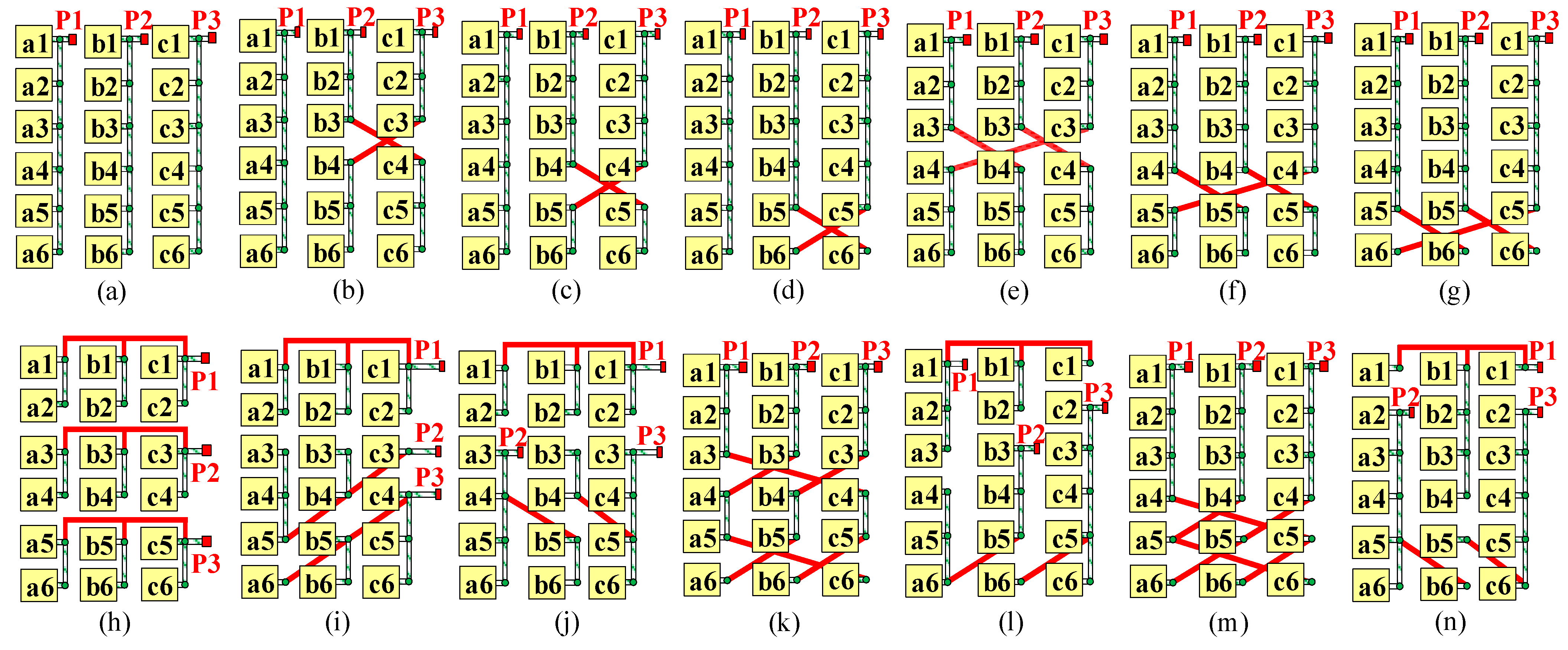
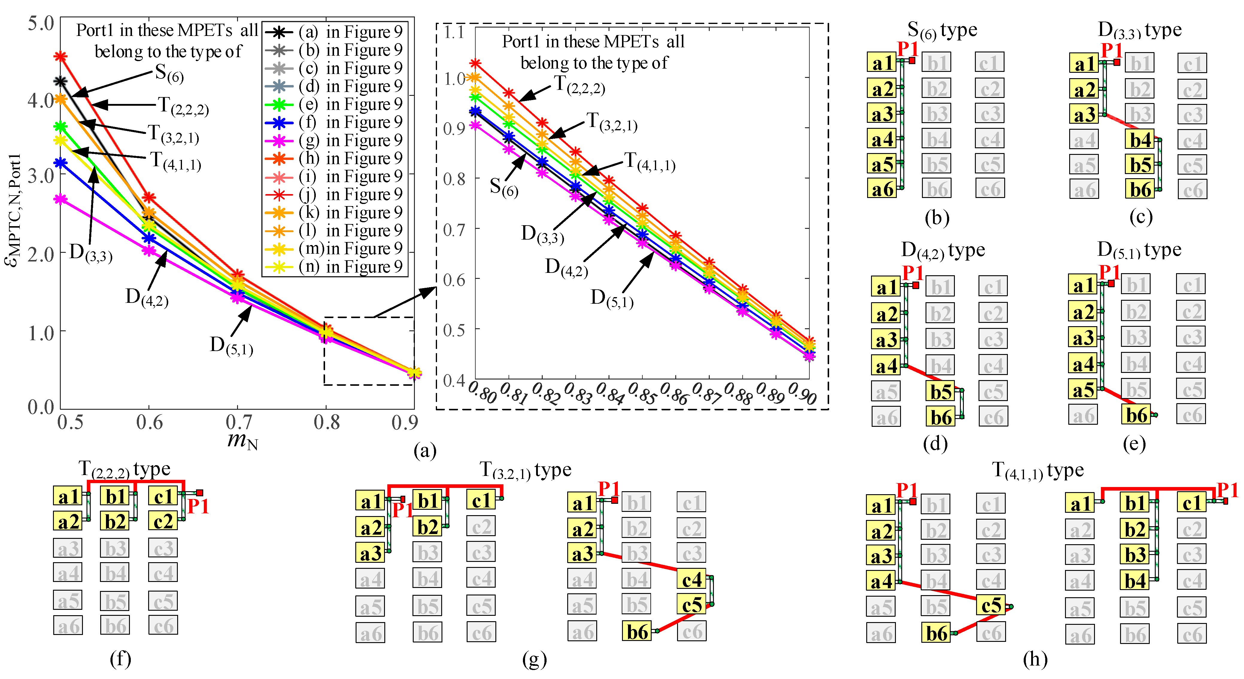
In this paper, the MPTC calculation results of LVDC ports in all of the IDBS-MPETs are obtained under mN = 0.5, 0.6, 0.7, 0.8 and 0.9. The IDBS-MPETs of N(6)P(3) (i.e., NH = 6 and NP = 3) are shown in Figure 9 and the MPTC calculation results of their LVDC ports are shown in Figure 10, and Table 5 and Table 6.
In order to make the MPTC calculation results more intuitive, the MPTC calculation results of S-Port, D-Port and T-Port will be shown in colors of different tones. The MPTC of S-Port will be shown in neutral colors (i.e., black or gray of different saturations). The MPTC of D-Port will be shown in cold colors (i.e., green, blue, cyan or purple of different saturations). The MPTC of T-Port will be shown in warm colors (i.e., red, orange, yellow or gold of different saturations). In the figures of the MPTC calculation results, the type of the LVDC port is indicated by S(ns)(ns1), D(nd)(nd1, nd2) and T(nt)(nt1,nt2,nt3). The structures of Port 1 belonging to these types are shown in Figure 10b–h.
The MPTC results of the LVDC ports of more than 80 typical IDBS-MPET topologies show the following:
(1)
The symmetrical LVDC port attains a larger MTPC value at every mN compared to the asymmetrical ones of the same type. As mentioned in Part B of Section 2, the T-Port can be divided into symmetrical T-Port and asymmetrical T-Port, the same as for the D-Port. As shown in Figure 10a, the MPTC value of the symmetrical T-Port (i.e., T(2,2,2)) is larger than that of asymmetrical T-Ports (i.e., T(3,2,1) and T(4,1,1)) at every mN. The MPTC value of the symmetrical D-Port (i.e., D(3,3)) is larger than that of asymmetrical D-Ports (i.e., D(4,2) and D(5,1)) at every mN. In addition, the MPTC value becomes smaller as the structure of the LVDC port becomes more asymmetrical. For example, the MPTC value of the T(4,1,1) type is smaller than that of the T(3,2,1) type at every mN. Therefore, the symmetrical T-Port is most preferable for the construction of the LVDC port, and the less asymmetrical T-Port can also be suitable as an option.
(2)
The symmetrical T-Port attains the largest MTPC value at every mN, and the most asymmetrical D-Port attains the smallest MTPC value at every mN. As shown in Figure 10a, the MPTC value of the symmetrical T-Port (i.e., T(2,2,2)) is the largest. The MPTC value of the most asymmetrical D-Port (i.e., D(5,1)) is the smallest. Moreover, as shown in Figure 10a and in the supplementary material of this paper, the MPTC value of asymmetrical D-Ports always becomes less than that of the T-Ports, symmetrical D-Ports and S-Ports. Therefore, it is best not to choose an asymmetrical D-Port to construct a LVDC port.
(3)
The MPTC value of the S-Ports is larger than that of the D-Ports when mN < 0.7, and larger than that of some extreme asymmetrical T-Ports when mN < 0.6. As shown in Figure 10a, when mN < 0.7, the MPTC value of the S-Port (i.e., S(6)) is larger than that of the D-Ports (i.e., D(3,3), D(4,2) and D(5,1)). When mN < 0.6, the MPTC value of the S-Port is even larger than that of the asymmetrical T-Ports (i.e., T(4,1,1)). The MPTC of the S-Port will become smaller than that of most T-Ports and the symmetrical D-Port when mN ≥ 0.7, whereas it is still larger or close to the value of the asymmetrical D-Port (i.e., D(4,2) and D(5,1)). Therefore, it is much better to choose an S-Port to construct an LVDC port rather than an asymmetrical D-Port.
(4)
Regardless of the type of LVDC port, the MPTC value increases with the reduction in mN. In industrial PET products, the mN is usually set between 0.7 and 0.9 [9,14,26]. As shown in Figure 10a, when mN is in the range from 0.8 to 0.9, the MPTC value of any type of LVDC port is less than 1. In order to improve the MPTC of the LVDC port, it is much better to set the mN of the IDBS-MPET in the range from 0.7 to 0.8 or even in the range from 0.6 to 0.8.
(5)
For the same type of LVDC port, the arrangement of modules in each phase does not affect the MPTC. As show in Figure 10g,h, both the T(3,2,1)- and T(4,1,1)-type LVDC port have two variants. As shown in Figure 10a, the two variants of the T(3,2,1)-type LVDC port have the same MPTC, and so does the T(4,1,1)-type LVDC port.
(6)
The variations in the MPTC among different configurations, especially the close performance between S(6) and the highest percentages in other types, can be attributed to the inherent design and operational characteristics of each configuration. For example, symmetrical configurations like T(2,2,2) generally offer a higher MPTC due to balanced power distribution among phases, while asymmetrical ones like D(5,1) might lag due to uneven load handling. The S(6) configuration, despite being a single-phase connection, leverages its design to maximize power transfer, thereby offering a compelling alternative for specific applications where compact design and high power-transfer capability are critical.

4.2. Three Topology Design Rules

Due to the limitations of NH, NP and PN,Portj, the LVDC ports in an IDBS-MPET cannot all be constructed as symmetrical T-Ports. The S-Port and D-Port also need to be used. Three topology design rules are derived from the MPTC results.
(1)
Topology design rule 1: when designing an IDBS-MPET, it is preferable that the LVDC ports are constructed as symmetrical and less asymmetrical T-Ports.
(2)
Topology design rule 2: when as many LVDC ports as possible have been designed based on topology design rule 1, it is preferable that the remaining LVDC ports are constructed as symmetrical D-Ports.
(3)
Topology design rule 3: when as many LVDC ports as possible have been designed based on topology design rule 1 and topology design rule 2, it is preferable that the remaining LVDC ports are constructed as S-Ports.

4.3. IDBS-MPET Design Scheme

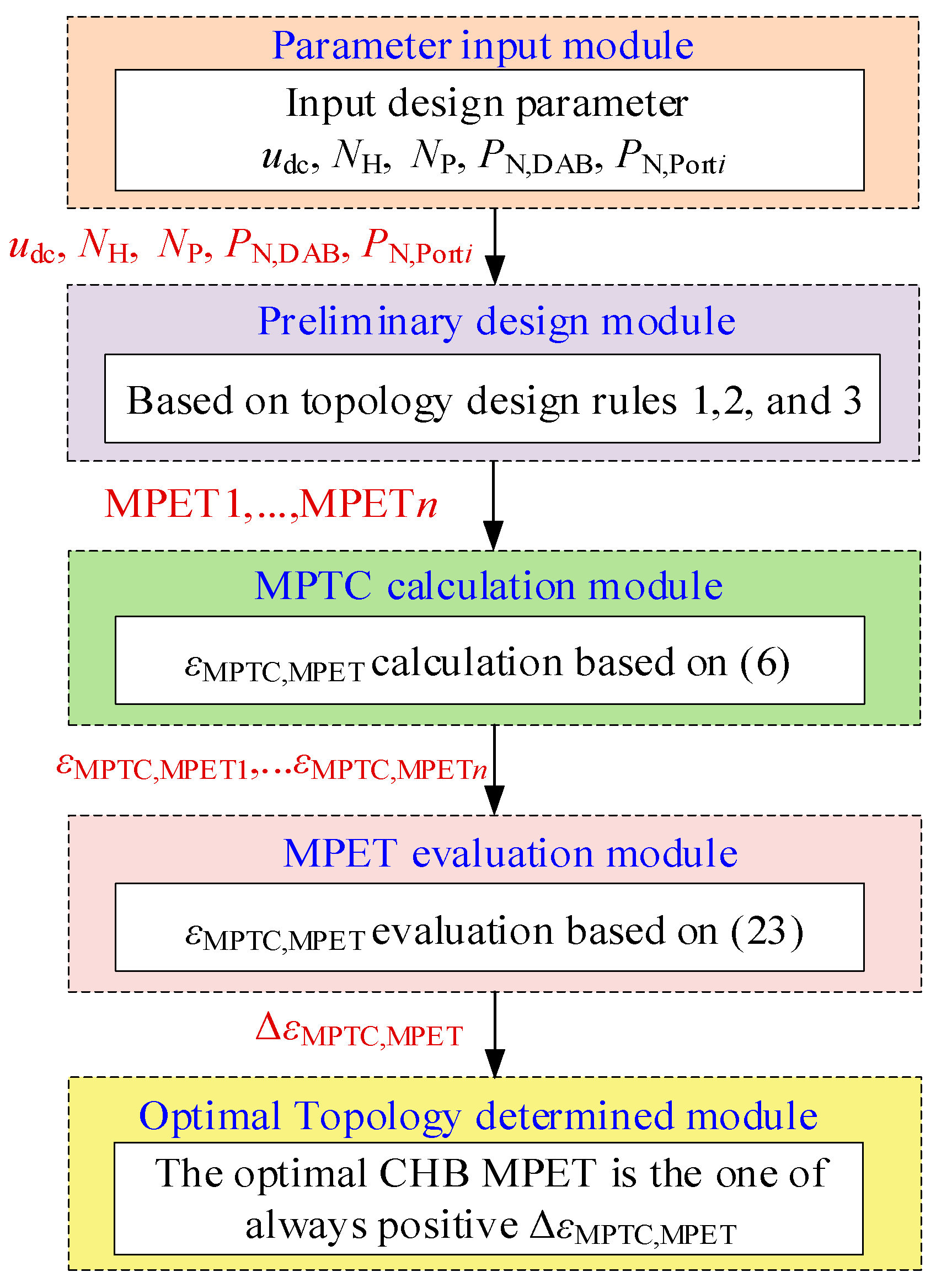
The IDBS-MPET design scheme is given in Figure 11. The basic idea of the design scheme is that a few IDBS-MPET topologies that conform to the three topology design rules are designed preliminarily, and then, the optimal one is determined by ΔεMPTC,MPET.
The IDBS-MPET design scheme contains five modules:
(1)
Parameter input module. The udc, NH can be designed based on the MVAC grid voltage. Previous studies have proved that 1200 V or 1700 V are identified as optimum blocking voltages of the power semiconductors [27]. Thus, the udc can be set around 600 V or 850 V. In industrial PET products, the mN is usually set between 0.7 and 0.9 [14,16], so NH can be determined by (22). The NP, PN,DAB and PN,Portj (j = 1…NP) can be designed based on the variety and the power demand of DGs and DC loads.
(2)
Preliminary design module. Several IDBS-MPETs are preliminarily designed based on the three topology design rules. As mentioned in Part A of this section, the asymmetrical T-Port may gain advantage or disadvantage over the symmetrical D-Port. Moreover, the range of the advantage of the symmetrical D-Port over the S-Port may be wide or narrow. Thus, more than one IDBS-MPET topology may emerge after the preliminary designing process. It is noted the topologies will not be too much. These topologies shall be systematically identified and enumerated as MPET1, MPET2, …, through MPETn, for ease of reference and subsequent analysis.
(3)
MPTC calculation module. The MPTCs of MPET1, …, MPETn are calculated based on (5), namely, εMPTC,MPET1, …, εMPTC,MPETn.
(4)
MPET evaluation module. In order to determine the optimal topology, the evaluation index ΔεMPTC,MPET is proposed. If two MPETs are under comparison, namely, the MPETx1 and the MPETx2, ΔεMPTC,MPET is defined as follows:
ε MPTC , MPET = Σ m N = 0.5 0.9 ( ε MPTC , MPET x 1 , m N ε MPTC , MPET x 2 , m N )
where εMPTC,MPETx1,mN is the εMPTC,MPET of MPETx1 on mN; εMPTC,MPETx2,mN is the εMPTC,MPET of MPETx2 on mN. The ΔεMPTC,MPET makes a comprehensive MPTC evaluation of the two MPETs on each mN. When the ΔεMPTC,MPET > 0, the MPETx1 emerges as preferable compared to MPETx2 and vice versa.
(5)
Optimal topology output module. Finally, the optimal IDBS-MPET is the one that always has a positive ΔεMPTC,MPET.

5. Evaluation Results

In this section, the optimal IDBS-MPET with NH = 6 and NP = 6 is designed by the proposed scheme. Moreover, the MPTC evaluation is conducted with the optimal IDBS-MPET and twelve other ones not designed by the proposed scheme to validate the effectiveness of the proposed design scheme.
In the parameter input module, design parameters are determined and listed in Table 7. In the preliminary design module, each LVDC port will be designed based on the three topology design rules.
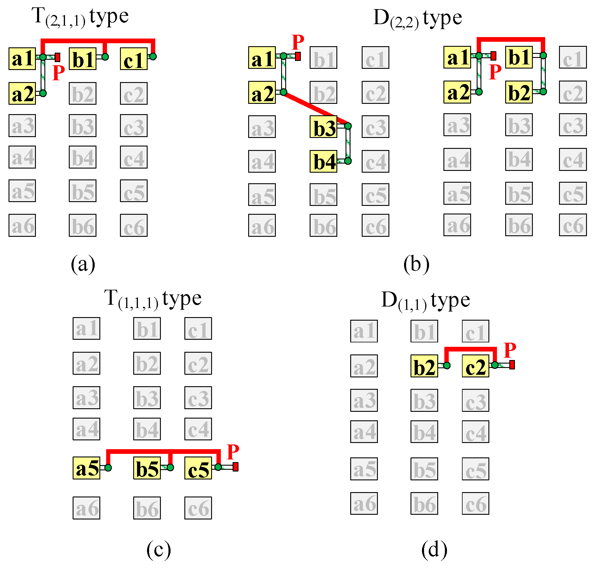
The structures of Port 1 to 6 are shown in Figure 12. Each of Port 1 and Port 2 consists of four DABs and both of them can be constructed as asymmetrical T-Ports (i.e., T(2,1,1)) or symmetrical D-Ports (i.e., D(2,2)). Each of Port 3 and Port 4 consists of three DABs and both of them will be constructed as symmetrical T-Ports (i.e., T(1,1,1)). Each of Port 5 and Port 6 consists of two DABs and both of them will be constructed as symmetrical D-Ports (i.e., D(1,1)).
By employing the proposed design methodology, each LVDC port achieves its maximum power transfer capability relative to other configurations. For the LVDC ports consisting of four DABs, the best type of configuration using the proposed methodology, i.e., T(2,1,1), and the worst type of configuration not using the proposed methodology, i.e., D(3,1), are shown in Table 8. Under every mN, especially when mN < 0.8, the LVDC port employing the proposed methodology exhibits a substantially higher maximum power and a greater absolute minimum power in comparison to alternative configurations.
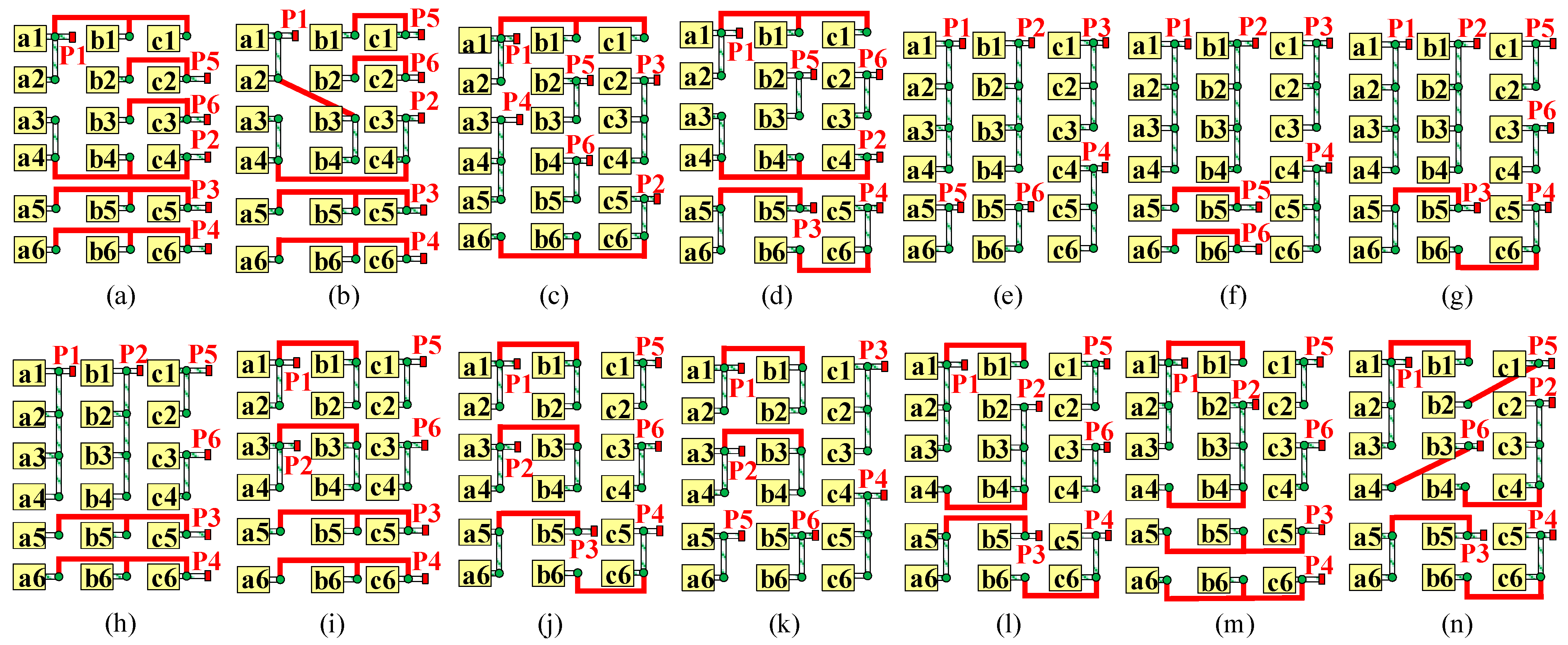
At last, there are two preliminary designed topologies of the IDBS-MPET with NH = 6 and NP = 6, the N(6)P(6)-D(2)(1,1)T(2)(1,1,1)T(2)(2,1,1) one, i.e., (a) in Figure 13, and the N(6)P(6)-D(2)(1,1)D(2)(2,2)T(2)(1,1,1) one, i.e., (b) in Figure 13. In the MPTC calculation module, the εMPTC,MPET of the two IDBS-MPETs is calculated and shown in Table 9. In the MPET evaluation module, the ΔεMPTC,MPET is calculated to be 1.94. Finally, in the optimal topology output module, the N(6)P(6)-D(2)(1,1)T(2)(1,1,1)T(2)(2,1,1) one emerges as the optimal IDBS- MPET with NH = 6 and NP = 6.
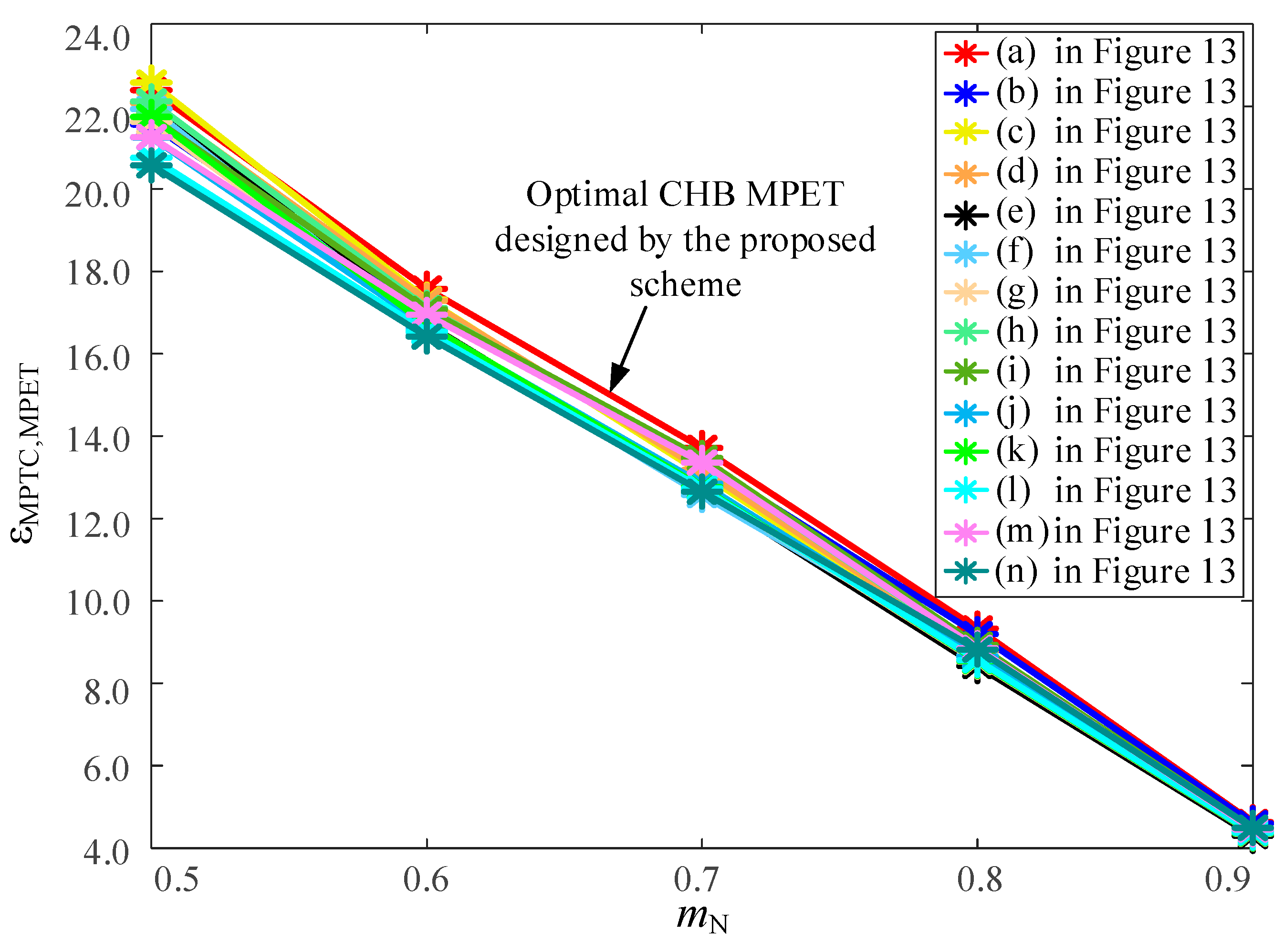
Twelve other IDBS-MPETs with NH = 6 and NP = 6 that are not designed by the proposed scheme are shown in (c)~(n) of Figure 13. The MPTC calculation results of the optimal one, namely, N(6)P(6)-D(2)(1,1)T(2)(1,1,1)T(2)(2,1,1), and twelve other IDBS-MPETs are shown in Figure 14. As shown in Table 9, the optimal IDBS-MPET designed by the proposed scheme emerges as the one which always has a positive ΔεMPTC,MPET, and thus, the effectiveness of the proposed design scheme is validated.

6. Discussion

This study presented a novel design scheme for IDBS-MPET topology aimed at maximizing the power transmission capability of low-voltage DC ports. The findings reveal significant implications for the design and operation of multiport power electronic transformers in hybrid AC/DC distribution systems. By categorizing LVDC ports into three basic types (S-Port, D-Port and T-Port) and establishing a design methodology based on the maximum power transmission capability (MPTC), this research contributes a systematic approach to enhance power balance and efficiency in MPET applications.
Comparative analysis with existing MPET configurations, such as those relying on a common DC bus structure, underscores the advantages of the proposed IDBS-MPET design. Specifically, the ability to directly construct each LVDC port by paralleling the output terminals of dual active bridge (DAB) converters eliminates the need for additional DC/DC converters, thereby reducing hardware costs and improving system efficiency. This approach not only addresses the challenge of power imbalance in IDBS-MPET systems but also offers a flexible and scalable solution for integrating diverse energy resources and loads in modern electrical distribution networks.
The proposed topology design rules, derived from extensive simulations of more than 80 typical IDBS-MPET topologies, offer clear guidelines for optimizing the structure of LVDC ports. These rules highlight the preference for symmetric T-Port, symmetric D-Port and S-Port configurations in order of their optimal power transmission capabilities. Such insights are invaluable for designers and engineers seeking to develop MPET systems that can accommodate varying power levels and voltage requirements while maintaining high efficiency and reliability.
Our research highlights the impact of the rated modulation ratio mN on the MPTC of the LVDC port in the IDBS-MPET. Specifically, we recommend setting mN in the range from 0.7 to 0.8, or even extending it to range from 0.6 to 0.8, contrary to the conventional range from 0.7 to 0.9 used in industrial PET products. Implementing this adjustment has several practical implications:
Optimized design. This adjustment allows for a more flexible and efficient design of PET systems, enabling them to accommodate a wider range of power levels and operational conditions.
Cost-effectiveness. By optimizing the MPTC, the proposed adjustment can lead to reductions in the size and cost of PETs, making them more competitive and appealing for industrial applications.
Future research could explore the integration of advanced control strategies and power electronics technologies to further enhance the performance and adaptability of IDBS-MPET systems. Additionally, real-world implementation and testing of the proposed topology in various operational scenarios would provide empirical evidence of its benefits and limitations, paving the way for further refinements and applications in the field of power electronics and energy distribution.

7. Conclusions

In this paper, a design scheme of IDBS-MPET topology is proposed based on the MPTC of the LVDC ports. Each LVDC port is directly constructed by paralleling the output terminals of DAB converters, eliminating the need for additional DC/DC converters. The LVDC ports are categorized into three basic types: S-Port, D-Port and T-Port. A design methodology for LVDC port structures is established, with the MPTC of the LVDC ports as the evaluation metric. Through extensive simulations of the MPTC in different LVDC port structures, three topology design rules for the IDBS-MPET are derived. Symmetric T-Ports, symmetric D-Ports and S-Ports, in that order, are the optimal structures for constructing low-voltage DC ports. The proposed method allows for the design of all LVDC port structures in an IDBS-MPET given the rated voltage of the H-bridge DC side, the number of H-bridges per phase, the rated power of the DAB converters, the number of LVDC ports and the rated power of each LVDC port, following the three topology design rules.

Supplementary Materials

The following supporting information can be downloaded at: https://www.mdpi.com/article/10.3390/en17051096/s1.

Author Contributions

Conceptualization, J.L. and F.X.; methodology, J.L. and F.X.; validation, J.L.; formal analysis, J.L. and F.X.; writing—original draft preparation, J.L.; writing—review and editing, F.X. and J.W.; supervision, J.W. All authors have read and agreed to the published version of the manuscript.

Funding

This research was funded by the National Natural Science Foundation of China (No. 52307193).

Data Availability Statement

The data presented in this study are available on request from the corresponding author.

Acknowledgments

Junchi Li thanks Rufeng Liu, Yiwei Pan, Geng Chen and Dan Huang for their valuable discussions and their helpful advice with this paper.

Conflicts of Interest

The authors declare no conflicts of interest.

References

  1. Li, K.; Wen, W.; Zhao, Z.; Yuan, L.; Cai, W.; Mo, X.; Gao, C. Design and implementation of four-port megawatt-level high-frequency-bus based power electronic transformer. IEEE Trans. Power Electron. 2020, 36, 6429–6442. [Google Scholar] [CrossRef]
  2. Liserre, M.; Perez, M.A.; Langwasser, M.; Rojas, C.A.; Zhou, Z. Unlocking the hidden capacity of the electrical grid through smart transformer and smart transmission. Proc. IEEE 2022, 111, 421–437. [Google Scholar] [CrossRef]
  3. Wen, W.; Li, K.; Zhao, Z.; Yuan, L.; Mo, X.; Cai, W. Analysis and control of a four-port megawatt-level high-frequency-bus-based power electronic transformer. IEEE Trans. Power Electron. 2021, 36, 13080–13095. [Google Scholar] [CrossRef]
  4. Li, Y.; Li, Y.W. The evolutions of multilevel converter topology: A roadmap of topological invention. IEEE Ind. Electron. Mag. 2021, 16, 11–18. [Google Scholar] [CrossRef]
  5. Huber, J.E.; Kolar, J.W. Applicability of solid-state transformers in today’s and future distribution grids. IEEE Trans. Smart Grid 2017, 10, 317–326. [Google Scholar] [CrossRef]
  6. Hu, Y.; Li, Z.; Zhang, H.; Zhao, C.; Gao, F.; Luo, L.; Luan, K.; Wang, P.; Li, Y.; Yuan, X. High-frequency-link current stress optimization of cascaded h-bridge-based solid-state transformer with third-order harmonic voltage injection. IEEE J. Emerg. Sel. Top. Power Electron. 2020, 9, 1027–1038. [Google Scholar] [CrossRef]
  7. Ruiz, F.; Perez, M.A.; Espinosa, J.R.; Gajowik, T.; Stynski, S.; Malinowski, M. Surveying solid-state transformer structures and controls: Providing highly efficient and controllable power flow in distribution grids. IEEE Ind. Electron. Mag. 2020, 14, 56–70. [Google Scholar] [CrossRef]
  8. Kolar, J.W.; Ortiz, G. Solid-state-transformers: Key components of future traction and smart grid systems. In Proceedings of the International Power Electronics Conference—ECCE Asia (IPEC 2014), Hiroshima, Japan, 18–21 May 2014; pp. 22–35. [Google Scholar]
  9. Chen, Y.; Shi, K.; Chen, M.; Xu, D. Data center power supply systems: From grid edge to point-of-load. IEEE J. Emerg. Sel. Top. Power Electron. 2022, 11, 2441–2456. [Google Scholar] [CrossRef]
  10. Zhao, B.; Song, Q.; Li, J.; Xu, X.; Liu, W. Comparative analysis of multilevel-high-frequency-link and multilevel-DC-link DC–DC transformers based on MMC and dual-active bridge for MVDC application. IEEE Trans. Power Electron. 2017, 33, 2035–2049. [Google Scholar] [CrossRef]
  11. Costa, L.F.; De Carne, G.; Buticchi, G.; Liserre, M. The smart transformer: A solid-state transformer tailored to provide ancillary services to the distribution grid. IEEE Power Electron. Mag. 2017, 4, 56–67. [Google Scholar] [CrossRef]
  12. Huang, A.Q.; Crow, M.L.; Heydt, G.T.; Zheng, J.P.; Dale, S.J. The future renewable electric energy delivery and management (freedm) system: The energy internet. Proc. IEEE 2010, 99, 133–148. [Google Scholar] [CrossRef]
  13. Zhao, B.; Song, Q.; Liu, W. A practical solution of high-frequency-link bidirectional solid-state transformer based on advanced components in hybrid microgrid. IEEE Trans. Ind. Electron. 2014, 62, 4587–4597. [Google Scholar] [CrossRef]
  14. Wang, D.; Tian, J.; Mao, C.; Lu, J.; Duan, Y.; Qiu, J.; Cai, H. A 10-kV/400-V 500-kVA Electronic Power Transformer. IEEE Trans. Ind. Electron. 2016, 63, 6653–6663. [Google Scholar] [CrossRef]
  15. Jia, H.; Xiao, Q.; He, J. An improved grid current and DC capacitor voltage balancing method for three-terminal hybrid AC/DC microgrid. IEEE Trans. Smart Grid 2018, 10, 5876–5888. [Google Scholar] [CrossRef]
  16. Ouyang, S.; Liu, J.; Wang, X.; Song, S.; Hou, X. Comparison of four power electronic transformer topologies on unbalanced load correction capacity. In Proceedings of the IEEE Energy Conversion Congress and Exposition (ECCE), Montreal, QC, Canada, 20–24 September 2015; pp. 3702–3709. [Google Scholar]
  17. Wang, X.; Liu, J.; Ouyang, S.; Meng, F. Research on unbalanced-load correction capability of two power electronic transformer topologies. IEEE Trans. Power Electron. 2014, 30, 3044–3056. [Google Scholar] [CrossRef]
  18. Iov, F.; Blaabjerg, F.; Clare, J.; Wheeler, P.; Rufer, A.; Hyde, A. Uniflex-PM–A key-enabling technology for future European electricity networks. Eur. Power Electron. Drives Assoc. J. 2009, 19, 6–16. [Google Scholar] [CrossRef]
  19. Watson, A.J.; Dang, H.Q.S.; Mondal, G.; Clare, J.C.; Wheeler, P.W. Experimental implementation of a multilevel converter for power system integration. In Proceedings of the 2009 IEEE Energy Conversion Congress and Exposition, San Jose, CA, USA, 20–24 September 2009; pp. 2232–2238. [Google Scholar]
  20. Zhao, T.; Wang, G.; Bhattacharya, S.; Huang, A.Q. Voltage and power balance control for a cascaded H-bridge converter-based solid-state transformer. IEEE Trans. Power Electron. 2012, 28, 1523–1532. [Google Scholar] [CrossRef]
  21. Yu, Y.; Konstantinou, G.; Hredzak, B.; Agelidis, V.G. Power balance optimization of cascaded H-bridge multilevel converters for large-scale photovoltaic integration. IEEE Trans. Power Electron. 2015, 31, 1108–1120. [Google Scholar] [CrossRef]
  22. Yan, Y.; Bai, H.; Foote, A.; Wang, W. Securing full-power-range zero-voltage switching in both steady-state and transient operations for a dual-active-bridge-based bidirectional electric vehicle charger. IEEE Trans. Power Electron. 2019, 35, 7506–7519. [Google Scholar] [CrossRef]
  23. Abuishmais, I.; Shahroury, F.R. Bidirectional dual active bridge for interfacing battery energy storage systems with DC microgrid. In Proceedings of the 2021 International Conference on Electrical, Computer and Energy Technologies (ICECET), Cape Town, South Africa, 9–10 December 2021; pp. 1659–1663. [Google Scholar]
  24. Shi, J.; Zhou, L.; He, X. Common-duty-ratio control of input-parallel output-parallel (IPOP) connected DC–DC converter modules with automatic sharing of currents. IEEE Trans. Power Electron. 2011, 27, 3277–3291. [Google Scholar] [CrossRef]
  25. Wang, M.; Zhang, X.; Zhao, T.; Ma, M.; Hu, Y.; Wang, F.; Wang, X. Harmonic compensation strategy for single-phase cascaded H-bridge PV inverter under unbalanced power conditions. IEEE Trans. Ind. Electron. 2020, 67, 10474–10484. [Google Scholar] [CrossRef]
  26. Dujic, D.; Zhao, C.; Mester, A.; Steinke, J.K.; Weiss, M.; Lewdeni-Schmid, S.; Chaudhuri, T.; Stefanutti, P. Power electronic traction transformer-low voltage prototype. IEEE Trans. Power Electron. 2013, 28, 5522–5534. [Google Scholar] [CrossRef]
  27. Huber, J.E.; Kolar, J.W. Optimum number of cascaded cells for high-power medium-voltage AC–DC converters. IEEE J. Emerg. Sel. Top. Power Electron. 2016, 5, 213–232. [Google Scholar] [CrossRef]
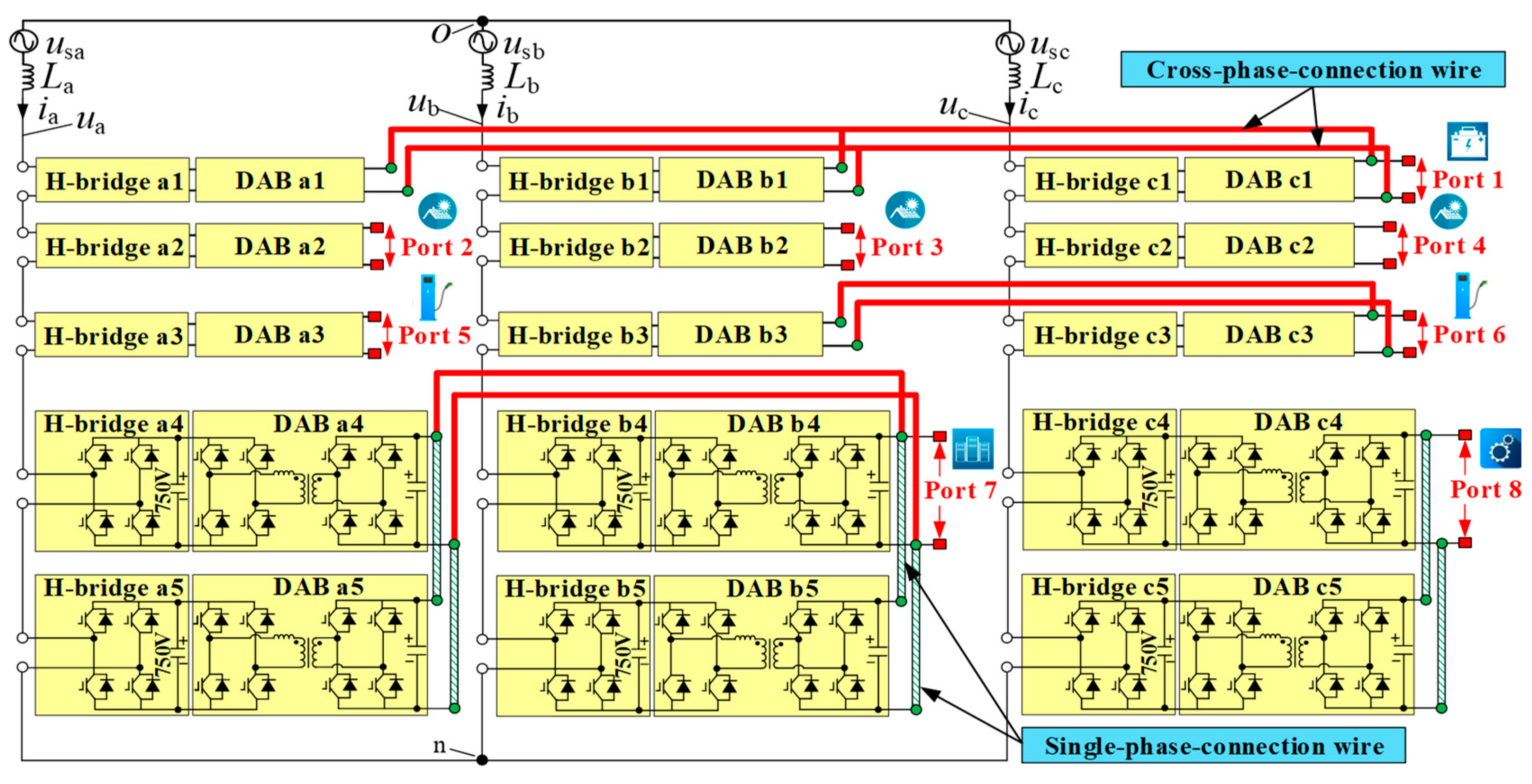
Figure 1. Independent DC bus structure multiport power electronic transformer (IDBS-MPET).
Energies 17 01096 g001
Figure 2. Common DC bus structure multiport power electronic transformer (CDBS-MPET).
Energies 17 01096 g002
Figure 3. Structure of DC/DC 1 to 8 in CDBS-MPET.
Energies 17 01096 g003
Figure 4. Total number of power semiconductors in IDBS-MPET and CDBS-MPET.
Energies 17 01096 g004
Figure 5. Basic structures of LVDC ports. (a) Single-phase connection port (S-Port). (b) Double cross-phase connection port (D-Port). (c) Triple cross-phase connection port (T-Port).
Energies 17 01096 g005
Figure 6. Graphical representation of LVDC ports. (a) General graphical representation of cascaded H-bridge and DAB. (b) S-Port. (c) D-Port. (d) T-Port.
Energies 17 01096 g006
Figure 7. Graphical representation and naming of IDBS-MPET in Figure 1.
Energies 17 01096 g007
Figure 8. Structure of H-bridge and DAB.
Energies 17 01096 g008
Figure 9. IDBS-MPETs of N(6)P(3). (a) N(6)P(3)-S(3)(6). (b) N(6)P(3)-S(1)(6)D(2)(3,3). (c) N(6)P(3)-S(1)(6)D(2)(4,2). (d) N(6)P(3)-S(1)(6)D(2)(5,1). (e) N(6)P(3)-D(3)(3,3). (f) N(6)P(3)-D(3)(4,2). (g) N(6)P(3)-D(3)(5,1). (h) N(6)P(3)-T(3)(2,2,2). (i) N(6)P(3)-T(1)(2,2,2)T(2)(3,2,1). (j) N(6)P(3)-D(2)(4,2)T(1)(2,2,2). (k) N(6)P(3)-T(3)(3,2,1). (l) N(6)P(3)-D(1)(3,3)D(1)(5,1)T(1)(3,2,1). (m) N(6)P(3)-T(3)(4,1,1). (n) N(6)P(3)-D(2)(5,1)T(1)(4,1,1).
Energies 17 01096 g009
Figure 10. MPTC and the structures of Port 1 in MPETs shown in Figure 9. (a) MPTC of Port 1. (b) Port 1 of S(6) type. (c) Port 1 of D(3,3) type. (d) Port 1 of D(4,2) type. (e) Port 1 of D(5,1) type. (f) Port 1 of T(2,2,2) type. (g) Port 1 of T(3,2,1) type. (h) Port 1 of T(4,1,1) type.
Energies 17 01096 g010
Figure 11. IDBS-MPET systematic design scheme.
Energies 17 01096 g011
Figure 12. Structure of LVDC ports in MPETs shown in Figure 13. (a) Port 1 of T(2,1,1) type. (b) Port 1 of D(2,2) type. (c) Port 1 of T(1,1,1) type. (d) Port 1 of D(1,1) type.
Energies 17 01096 g012
Figure 13. IDBS-MPET with NH = 6 and NP = 6, namely, N(6)P(6). (a) N(6)P(6)-D(2)(1,1)T(2)(1,1,1)T(2)(2,1,1) is one of the preliminary designed topologies and finally emerges as the optimal one designed by the proposed design scheme. (b) N(6)P(6)-D(2)(1,1)D(2)(2,2)T(2)(1,1,1) is the other preliminary designed topology. (c) N(6)P(6)-S(2)(2)S(2)(3)T(2)(2,1,1). (d) N(6)P(6)-S(2)(2)D(2)(2,1)T(2)(2,1,1). (e) N(6)P(6)-S(2)(2)S(2)(3)S(2)(4). (f) N(6)P(6)-S(2)(3)S(2)(4)D(2)(1,1). (g) N(6)P(6)-S(2)(2)S(2)(4)D(2)(2,1). (h) N(6)P(6)-S(2)(2)S(2)(4)T(2)(1,1,1). (i) N(6)P(6)-S(2)(2)D(2)(2,2)T(2)(1,1,1). (j) N(6)P(6)-S(2)(2)D(2)(2,1)D(2)(2,2). (k) N(6)P(6)-S(2)(2)S(2)(3)D(2)(2,2). (l) N(6)P(6)-S(2)(2)D(2)(2,1)D(2)(3,1). (m) N(6)P(6)-S(2)(2)D(2)(3,1)T(2)(1,1,1). (n) N(6)P(6)-D(2)(1,1)D(2)(2,1)D(2)(3,1). The IDBS-MPETs in (cn) are not designed by the proposed design scheme and they are used to be compared with (a) by εMPTC,MPET to validate the effectiveness of the proposed design scheme.
Energies 17 01096 g013
Figure 14. MPTC calculation results of IDBS-MPETs with NH = 6 and NP = 6, namely, N(6)P(6).
Energies 17 01096 g014
Table 1. Devices connected to the IDBS-MPET and CDBS-MPET.
Port NameDevices Connected to Port 1 to 8Nominal Power and Voltages
Port 1Energy storagePN,Port1 = 240 kW, VN,Port1 = 750 V
Port 2PVPN,Port2 = 80 kW, VN,Port2 = 600 V
Port 3PVPN,Port3 = 80 kW, VN,Port3 = 600 V
Port 4PVPN,Port4 = 80 kW, VN,Port4 = 600 V
Port 5EV fast chargerPN,Port5 = 80 kW, VN,Port5 = 400 V
Port 6EV ultra-fast chargerPN,Port6 = 160 kW, VN,Port6 = 800 V
Port 7Data centerPN,Port7 = 320 kW, VN,Port7 = 400 V
Port 8Industrial loadPN,Port8 = 160 kW, VN,Port8 = 750 V
Table 2. Circuit parameters of the IDBS-MPET and CDBS-MPET.
Circuit ParametersValue
Nominal grid line-to-line voltage RMS2500 V
Number of H-bridge cells per phase5
H-bridge DC voltage 750 V
DAB high-frequency transformer turn ratio1:1
Nominal power of H-bridgePN,Hbridge = 80 kW
Nominal power of DABPN,DAB = 80 kW
Table 3. The number of IPOP DABs in DC/DC 1 to 8 in the CDBS-MPET.
NameNumber of IPOP DABs
DC/DC 13
DC/DC 21
DC/DC 31
DC/DC 41
DC/DC 51
DC/DC 62
DC/DC 74
DC/DC 82
Table 4. Naming of LVDC ports.
Kinds of LVDC PortsNaming
S-PortS(ns)(ns1)
D-PortD(nd)(nd1, nd2)
T-PortT(nt)(nt1,nt2,nt3)
Table 5. MPTC results of LVDC ports in the IDBS-MPET with NH = 6 and NP = 3.
mNT(2,2,2)T(3,2,1)T(4,1,1)D(3,3)D(4,2)D(5,1)S(6)
0.54.4983.9573.4303.6063.1422.6794.181
0.62.6992.5092.3462.3172.1812.0232.447
0.71.7181.6391.5781.5421.4831.4171.541
0.81.0281.0000.9750.9610.9340.9050.930
0.90.4760.4700.4640.4620.4530.4450.444
Table 6. The percentage of the MPTC results of six kinds of LVDC ports relative to the MPTC results of T(2,2,2)-type LVDC port in the IDBS-MPET with NH = 6 and NP = 3.
mNT(3,2,1) T(4,1,1)D(3,3)D(4,2)D(5,1)S(6)
0.587.97%76.26%80.17%69.85%59.56%92.95%
0.692.96%86.92%85.85%80.81%74.95%90.66%
0.795.40%91.85%89.76%86.32%82.48%89.70%
0.897.28%94.84%93.48%90.86%88.04%90.47%
0.998.74%97.48%97.06%95.17%93.49%93.28%
Table 7. Parameters of IDBS-MPET with NH = 6 and NP = 6.
Design ParametersValue
udc750 V
NH6
NP6
PN,DAB50 kW
PN,Port1200 kW
PN,Port2200 kW
PN,Port3150 kW
PN,Port4150 kW
Table 8. The maximum and minimum power of different types of LVDC ports consisting of four DABs in the IDBS-MPET in Figure 12.
Port TypemN = 0.9mN = 0.8mN = 0.7mN = 0.6mN = 0.5
Pmax/kWPmin/kWPmax/kWPmin/kWPmax/kWPmin/kWPmax/kWPmin/kWPmax/kWPmin/kW
T(2,1,1)229.4110.9269.023.6324.8−61.8409.3−145.4551.4−209.0
S(4)229.4119.7269.249.6325.5−17.1411.7−84.3559.8−154.9
D(2,2)229.4113.8268.536.7323.2−30.4404.8−88.0539.0−138.3
D(3,1)229.2116.7267.643.8319.8−22.6393.8−85.8505.3−122.6
Table 9. MPTC results of the IDBS-MPETs with NH = 6 and NP = 6.
mNεMPTC,MPET
Figure 13aFigure 13bFigure 13cFigure 13dFigure 13eFigure 13fFigure 13gFigure 13hFigure 13iFigure 13jFigure 13kFigure 13lFigure 13mFigure 13n
0.522.3921.5622.5822.0822.1221.9421.6322.1221.7521.2521.7520.7621.2520.57
0.617.5816.9617.3217.2916.316.6116.7017.1117.0816.6716.7016.5416.9516.42
0.713.7113.3813.0913.1812.6512.5712.7413.3613.4712.8512.7612.7413.3512.65
0.89.339.198.688.788.428.688.528.818.948.648.548.568.868.82
0.94.634.604.394.444.304.424.354.434.494.414.364.384.464.50
Disclaimer/Publisher’s Note: The statements, opinions and data contained in all publications are solely those of the individual author(s) and contributor(s) and not of MDPI and/or the editor(s). MDPI and/or the editor(s) disclaim responsibility for any injury to people or property resulting from any ideas, methods, instructions or products referred to in the content.