
Minimum Power Input Control for Class-E Amplifier Using Depletion-Mode Gallium Nitride High Electron Mobility Transistor

1
Department of Material Science and Engineering, National Chiao Tung University, Hsinchu 30010, Taiwan
2
Mechanical and Mechatronics Systems Research Laboratories, Industrial Technology Research Institute, Hsinchu 31040, Taiwan
3
Department of Mechanical Engineering, National Chiao Tung University, Hsinchu 30010, Taiwan
*
Author to whom correspondence should be addressed.
Energies 2021, 14(8), 2302; https://doi.org/10.3390/en14082302
Submission received: 19 March 2021
/
Revised: 12 April 2021
/
Accepted: 15 April 2021
/
Published: 19 April 2021
(This article belongs to the Special Issue Modelling of Wireless Power Transfer II)
Abstract
:In this study, we implemented a depletion (D)-mode gallium nitride high electron mobility transistor (GaN HEMT, which has the advantage of having no body diode) in a class-E amplifier. Instead of applying a zero voltage switching control, which requires high frequency sampling at a high voltage (>600 V), we developed an innovative control method called the minimum power input control. The output of this minimum power input control can be presented in simple empirical equations allowing the optimal power transfer efficiency for 6.78 MHz resonant wireless power transfer (WPT). In order to reduce the switching loss, a gate drive design for the D-mode GaN HEMT, which is highly influential for the reliability of the resonant WPT, was also produced and described here for circuit designers.
1. Introduction
Class-E power amplifiers perform well in wireless power transfer (WPT) applications [1] because of their simple topology as well as high efficiency under zero voltage switching (ZVS) and zero voltage derivative switching (ZVDS) conditions. Thus, they have been used in various applications, such as battery charging [2], drones [3], LED lighting [4], and biomedicine [5]. Many studies have demonstrated the excellent performance of class-E power amplifiers [6,7], particularly when gallium nitride high electron mobility transistors (GaN HEMTs) are used [7,8,9,10,11]. GaN HEMTs provide high efficiency and performance due to their exceptional characteristics, such as low gate charge loss [7] and gate-source capacitance, which almost produce an ideal ZVS [8,9].
However, the performance of class-E power amplifiers is affected by load variation in addition to various non-ideal factors [12]. In response, different strategies have been proposed to optimize class-E amplifiers to increase operating efficiency and extend the transfer distance. These strategies involve a tuning couple [13]; the tuning duty ratio and frequency in relation to inductors and capacitors [14]; the control and compensation of variations in coupling and load impedance [10,11]; the coupling structure [15]; and the addition of transmitters [16,17]. In addition, a study proposed an analytical method that accounts for non-ideal factors (such as the inductance resistance, on resistance, and leakage current) in order to reduce the difference between calculated and actual values [18]. Moreover, although the use of GaN HEMTs in class-E power amplifiers improves efficiency and performance, a compatible and suitable gate driver must be designed to drive the GaN HEMT [19,20]. To this end, the charge pump gate drive presented by Ishibashi [20] is useful for driving the depletion (D)-mode GaN HEMT in a class-E amplifier.
Previous studies have proposed several laboratory-fabricated D-mode GaN HEMTs in cascade configurations [21,22]. To fully exploit the advantages of fabricated GaN HEMTs in class-E amplifiers, this study used a D-mode GaN HEMT with a charge pump gate driver. Specifically, in this study, the equivalent circuit of a class-E amplifier with a D-mode GaN HEMT was experimentally tested. In addition, based on the equivalent circuit, the characteristics of a fabricated D-mode GaN HEMT and the parameter of a compatible charge pump gate driver for the D-mode GaN HEMT were included in analyses to improve practicability. We continue on our work presented in [23] to optimize the operation for each scenario by using the proposed minimum power input control. The demo of the ZVS manual operation was provided in the previous article [23]. Previous studies have also proposed their own unique methods to achieve the high efficiency class-E power amplifier for WPT systems. The PTE of the TX-coil with an NIC [24] was much higher than that of a conventional WPT system. A class-E PA [25], based on the load-pull and impedance-transformation technique, showed a high-efficiency WPT for a wide load range. In this study, a simple look-up table, selecting the best combination and procedure of different duty cycles, frequencies, and VDDs, was used to yield a quick response and optimize efficiency in class-E amplifiers. This paper is organized as follows. The design of the D-mode GaN HEMT gate drive for the wireless power transfer is sensitive to parameters such as parasitic capacitances, output characteristic, transfer characteristic, and leakage current. Therefore, the fabrication conditions and parameters of the D-mode GaN HEMT are introduced in Section 2.1 in order to explain the design for a gate drive compatible with wireless power transfer. The design of the gate drive for the D-mode GaN HEMT is highly influential for the reliability of the resonant WPT. Taking into account the electrical characteristics of the fabricated D-mode GaN HEMT, the design of the charge pump gate drive for the D-mode GaN HEMT is presented in Section 2.2. Finally, the class-E amplifier with a charge pump gate drive circuit, and the proposed minimum power input control, are described in Section 2.3 and Section 2.4. Section 3 presents the experimental verification of resonant WPT with minimum power input control, and the conclusions are presented in Section 4.
2. Materials and Methods
In our previous paper [23], the mathematical derivation of the ZVS control of a class-E WPT unit was proposed. As stated in [23], one of the critical issues for WPT is dealing with the switching loss of the GaN HEMT transistor. The switching loss is mainly caused by GaN HEMT characteristics, including the output parasitic capacitance Coss and the input parasitic capacitance Ciss. Hence, the D-mode GaN HEMT characteristics, which are provided in Section 2.1, must be carefully studied and examined before and after the packaging. Nevertheless, the parasitic capacitance variations between turn-on and turn-off are the dominant factor for the switching loss. Hence, the gate driver design methodology is provided in Section 2.2. The design of the charge pump gate drive for the D-mode GaN HEMT is critical for class-E WPT efficiency. With regard to the maximum power transfer, we need to understand how the impedance matching mechanism is adjusted through the resonant frequency ωo, which is discussed in Section 2.4. Finally, we introduce a method called minimum power input control that functions by controlling the duty ratio δ, given in Section 2.5, to ensure the best power transfer efficiency (PTE), which implies the high PDL associated with a low switching loss. Figure 1 shows a flowchart of the key characteristic parameters for achieving the minimum power input control which is introduced in the following sections.
2.1. D-Mode GaN HEMT
Figure 2a illustrates the transfer characteristics of the fabricated D-mode GaN HEMT device when VG = −10 to 1 V, with VD = 10 V in Figure 2b. The threshold voltage given by the tangent of the ID–VG was found to intersect at −7 V. Therefore, the turn-on voltage of the D-mode GaN HEMT, vGS,ON, was recorded at −7 V. The maximum allowable gate voltage VGS,max was tested under the condition of |VGS,max| < 30 V. According to the leakage current due to different voltages, COSS = CGD + CDS varied, albeit only slightly, in the turn-on and turn-off periods. Furthermore, as the D-mode GaN HEMT had no body diode, the leakage current only flowed when vDS was negative. Table 1 summarizes the characteristics of the D-mode GaN HEMT.
The main reasons that the GaN HEMT is well-suited for WPT applications are that (1) it can perform high frequency switching with low switching loss; (2) it possesses no body diode; and (3) it involves low Ciss and Coss variation. The characteristic of have no body diode can ease the ZVS control and provide low energy loss during class-E switching operations. The Ciss and Coss variations of MOSFET can be as high as several hundred times between turn-on and turn-off. As for the GaN HEMT, Table 2 summarizes the parasitic capacitance of the D-mode GaN HEMT before packaging. The parasitic capacitances were nearly one-third of the MOSFET. The parasitic capacitance value and its variation were different for different packaging. For instance, the TO247, as shown in Figure 3b, yielded smaller capacitance than the TO220 shown in Figure 3a. Both types of packaging showed that the capacitance variation between turn-off at low VDS and turn-on at high VDS becomes smaller as the switching frequency increases. This is very good for resonant WPT in which the switching frequency is targeted at 6.78 MHz. In this study, the GaN HEMT in the TO220 packaging was used as it resulted in a smaller size than the TO247 packaging.
The design of the D-mode GaN HEMT gate drive for the wireless power transfer is sensitive to parameters including the gate-drain parasitic capacitance Crss (=CGD) and the gate input parasitic capacitance Ciss (=CGD +CGS). It is preferable for these parasitic capacitances to be as small as possible to enable higher frequency switching without much switching loss. On the other hand, the drain-source parasitic capacitance CDS incorporated with C2 and L2 forms a useful LC tank for the power transfer unit (PTU), which needs to be as constant as possible during the time the transistor is switching on and off. All the parasitic capacitances are closely related to the GaN HEMT design, including the thickness of the epitaxial structure of the GaN device. The resulting output characteristic in Figure 2b determines the RD,on related to the efficiency of the wireless power transfer. The transfer characteristic in Figure 2a shows the preferable vGS control range. It is preferable for the turn-on voltage vGS,ON to be as near to zero as possible to reduce the voltage level of the power supply for the gate drive.
2.2. Design of Charge Pump Gate Drive for D-Mode GaN HEMT
In order to design the D-mode GaN HEMT gate drive for class-E amplifiers, Ishibashi’s [20] charge pump gate drive was adopted in this study. The leakage current is critical to the charge pump reservoir dynamics, which result from the reverse saturation current of the Schottky barrier diodes (SBD), which is preferably kept as small as possible. The disadvantage of the charge pump circuit—the current leaking through the diode reverse saturation current—causes no harm to the high frequency switching. However, the class-E amplifier has the additional disadvantage of CGD being connected to the high voltage switching of vDS.
In a p–n junction diode, two types of capacitance occur: transition capacitance (CT) and diffusion capacitance (CD):
Cj0 = CT + CD,
In a forward-biased diode, CD, which is the focus of the following derivation, is much larger than the CT. Furthermore, the gate drive vs is high, and the current iG passes from VGH to VSS, which, for simplicity, is taken as the ground. The current iG passes from VGL to VSS when vs is low. As shown in Figure 4, we first assumed that VDS is floating and that RG,p = RG. In the gate drive state, vs is high and vG,h = 0.7 V, according to the diode forward-threshold voltage (built-in potential). The charge on the gate and diode side is:
QG,h = (CGS + Cj0)·vG,h,
The charge on the capacitor side is:
QC,h = CC·(VGH − vG,h),
The steady state gate voltage when the gate is turning off is:
vG,l = QC,l/(CGS + Cj0) = −QC,l/CC + VGL,
Assuming that CC >> CGS + Cj0 and VGL = 0 V, vG,h is small compared with VGH.
QC,l ≈ −CC·VGH,
vC,l ≈ VGH,
The leaking current in the charge pump occurs due to the diode reverse saturation current. When vDS is connected to a half sine voltage such that
the charge pump requires some amount of negative charge, which must be quickly supplied, because of CGD (the Miller capacitor) when vDS is increasing to a high voltage and the gate is turning off. The charge pump must also retract the same quantity of negative charges when the gate is turning on. Thus, in such dynamic behavior, the resulting effect is the Miller plateau: a low voltage surge occurs when the gate is turning on, and the period in the Miller plateau increases when the gate is turning off. As shown in Figure 5, when RG,p is too high (as indicated by the dotted line), RG,p causes a negative voltage surge due to the rapid retraction of negative charges through CGD and CC to RG,p. The negative voltage can potentially surge down to lower than −VGS,max and cause the gate source to break down. In such cases, RG,p must be reduced to prevent a large voltage drop in vG,h when the gate is turning on; the corresponding design parameters for the gate drive are shown in Table 3. The ideal gate source voltage for 6.78 MHz switching is also indicated by a dark solid line in Figure 5. Using the D-mode GaN HEMT as the switching device, the resonance mechanism for proper resonant frequency is a function of the duty cycle settings based on the hypotheses of zero voltage control and zero current control for the class-E amplifier [23]. ZVS and ZCS are achieved by adjusting both the duty cycle and resonant frequency to comply with the known phenomenon in GaN HEMT control, including the Miller plateau and current clamp in the gate drive design.
vDS ≈ 0 V when vs is high, vDS ≈ VDS,maxsin(ωot) when vs is low
2.3. Class-E Amplifier Circuit
Class-E amplifiers, as shown in Figure 6, have been used in 6.78 MHz resonant WPT applications. In this study, the actual load ZL for a wireless power transfer system was considered to be the mutual inductance in parallel with the equivalent impedance of the receiver side. For simplicity in exposition, we let the load RL be purely resistive. In the circuitry, the capacitor CDS is the parasitic capacitor of the D-mode GaN HEMT. As the GaN HEMT contains no body diode, (1) a current path where vDS is negative is impossible and (2) the resonant current i2 can be sinusoidal with low total harmonic distortion (THD). In the equivalent circuit, the input and output power of the class-E amplifier are defined as Pin = i1VDD and Pout = i2vL, respectively. The WPT experimental layout is shown in Figure 7a, and the charge pump gate driver for the D-mode GaN HEMT is shown in Figure 7b. The circuit parameters are shown in Table 4.
PWM Control and Circuit Response
In this study, the class-E amplifier circuit was considered in terms of two aspects: the switching power supply and impedance loading. The duty cycle of switching is denoted δ (i.e., the pulse width is δT (Figure 8a)). The SPICE analysis is shown in Figure 8b.
The switch was operated at a frequency of ωo = 2π/T. In the steady state, the output current is i2 = I2 sin(ωot + β) + I2,a cos(2ωot + β). The higher order terms I2,a << I2 cause the sinusoidal output to be asymmetric on its upswing and downswing wave forms. An example in which β = −180°, I2 = 1, and I2,a = 0.15, which are often seen in experiments, is shown in Figure 9a. The SPICE analysis is shown in Figure 9b.
In practice, the vGS signal of the class-E amplifier, as shown in Figure 10, is different from that of the SPICE analysis simulation. The output signal from the gate drive was no longer a square wave when the gate driver input signal from the PWM was a square wave between 0 and 5 V. The distortion of the gate drive output vGS is due to the input parasitic capacitance Ciss. Since the Ciss is relatively small at the high drain-source voltage vDS, as shown in Figure 3, compared to the Ciss at the low drain-source voltage, the turn-off delay time td,off is therefore larger than the turn-on delay time td,on. The actual duty ratio is larger than the designed duty ratio. Thus an emperical result, and not just the SPICE model simulation result alone, was required to compensate in the design. Knowledge about the device characteristics, especially the parasitic capacitance variation resulting from different packaging and different switching frequencies, is essential to control resonant WPT via a class-E amplifier.
2.4. Maximum Power Transfer
The equivalent circuit of the wireless power transfer for a single PTU transferring power to a single PRU is shown in Figure 11. The resonant frequency ωo was selected to yield the best impedance matching between ZPTU(jωo) and ZPRU(jωo) in order to obtain the maximum power transfer, which is also referred to as the maximum amount of power delivered to the load (PDL). The equivalent turn ratio a within the equivalent circuit for the wireless power transfer is a function of the distance between PTU and PRU. Hence, ωo must be controlled from time to time to achieve the impedance matching condition when the PRU is moving. In a closed loop control, to tune the resonant frequency ωo, the Airfuel Alliance recommends obtaining the required feedback of the actual power reading of the PRU via a 2.4 GHz communication network.
The PDL is also a function of VDS,max of the switching power supply circuit shown in Figure 6. We need a high VDS,max to enable linkage travel for the magnetic flux in the air, linking it to the PRU antenna coil. From [23], the VDS,max is derived into a function of the duty ratio δ, as shown in Figure 12. Theoretically, the VDS,max is a monotonically increasing function in terms of the duty ratio δ. On the other hand, while the switching loss of the D-mode GaN HEMT also increases with the VDS,max, the power transfer efficiency degrades due to the high VDS,max. The reason that the switching loss of the D-mode GaN HEMT increases is that the GaN HEMT has no body diode. There is really only one disadvantage of the GaN HEMT having no body diode: a higher reverse voltage drop. The reverse voltage drop of a GaN HEMT includes a resistive element arising from the channel resistance and threshold voltage. The voltage drop in a high voltage GaN HEMT can be as much as several volts when conducting large currents, which is larger than the equivalent drop in a MOSFET. Thus, we have a situation in which there is a trade-off between a high PDL and a high switching loss in terms of the duty ratio δ.
In practice, when we monitor the power input of the PTU, we see the power input increase due to either the mismatching of the impedances, resulting in low PDL in the low duty ratio δ region, or the high switching loss from the high VDS,max in the high duty ratio δ region. The minimum power input, which trades off both deficiencies, is the optimal solution. In the following section, we introduce an empirical technique to locate the optimal duty ratio δ and achieve the best power transfer efficiency, which implies the high PDL associated with a low switching loss.
2.5. Minimum Power Input Control
The minimum power input control of a class-E amplifier can be obtained experimentally. A specific power transmitter unit, with its equivalent parameters, is detailed in Table 4. We completed a set of 70 experiments and interpolated the results (Figure 13). In the experiments, VDD = 108 V, nominal resonant frequency = 4.12 MHz, and δ% (nominal duty ratio) = 30%. We calculated the minimum power points, which are indicated by red dots in Figure 13 and corresponded to the lowest power loss from Coss to the ground in the switching. The experiment was extended to different input voltages VDD. The results are shown in Figure 14. In WPT applications, higher input voltages VDD are required for greater power transfer distances. Conversely, power input Pin increases with the distance between the PTU and power receiver unit (PRU). Furthermore, in cases of multiple PRUs, the power input Pin must be increased accordingly to supply sufficient power to the PRUs. We thus formulated our minimum control strategy according to the following steps:
(1) Due to the power transfer query issued by the PRU, we determined the input voltage VDD according to the measured distance between the PTU and PRU.
(2) Due to the immediate power input Pin required for all PRUs, we determined the duty cycle δ (or duty ratio) according to the empirical data in Figure 14.
(3) From the duty ratio δ% calculated in step 2, we determined the resonant frequency f0 according to the empirical data in Figure 15.
The minimum power input Pin is supplied to the WPT based on the empirical data or equations in Figure 14 and Figure 15, which guarantees optimal power transfer efficiency. The minimum power input control is equivalent neither to conventional ZVS nor to zero current switching because of the absence of a body diode in the D-mode GaN HEMT. The energy stored in the CDS is not released to ground when vDS is negative. However, the minimum power input control minimizes the energy stored in the CDS when the gate is turned on, which is like the ZVS control. A more important feature of our design is that almost all energy loss in the class-E amplifier is due to switching loss. Thus, the power loss on the transistor switched-off time, which is the product of the drain current with the vDS, is the key factor affecting the minimum power input control. The power loss is related to the gate drive design and the parasitic capacitance of the D-mode GaN HEMT; it is also absent in conventional ZVS control derivations.
3. Resonant WPT Results
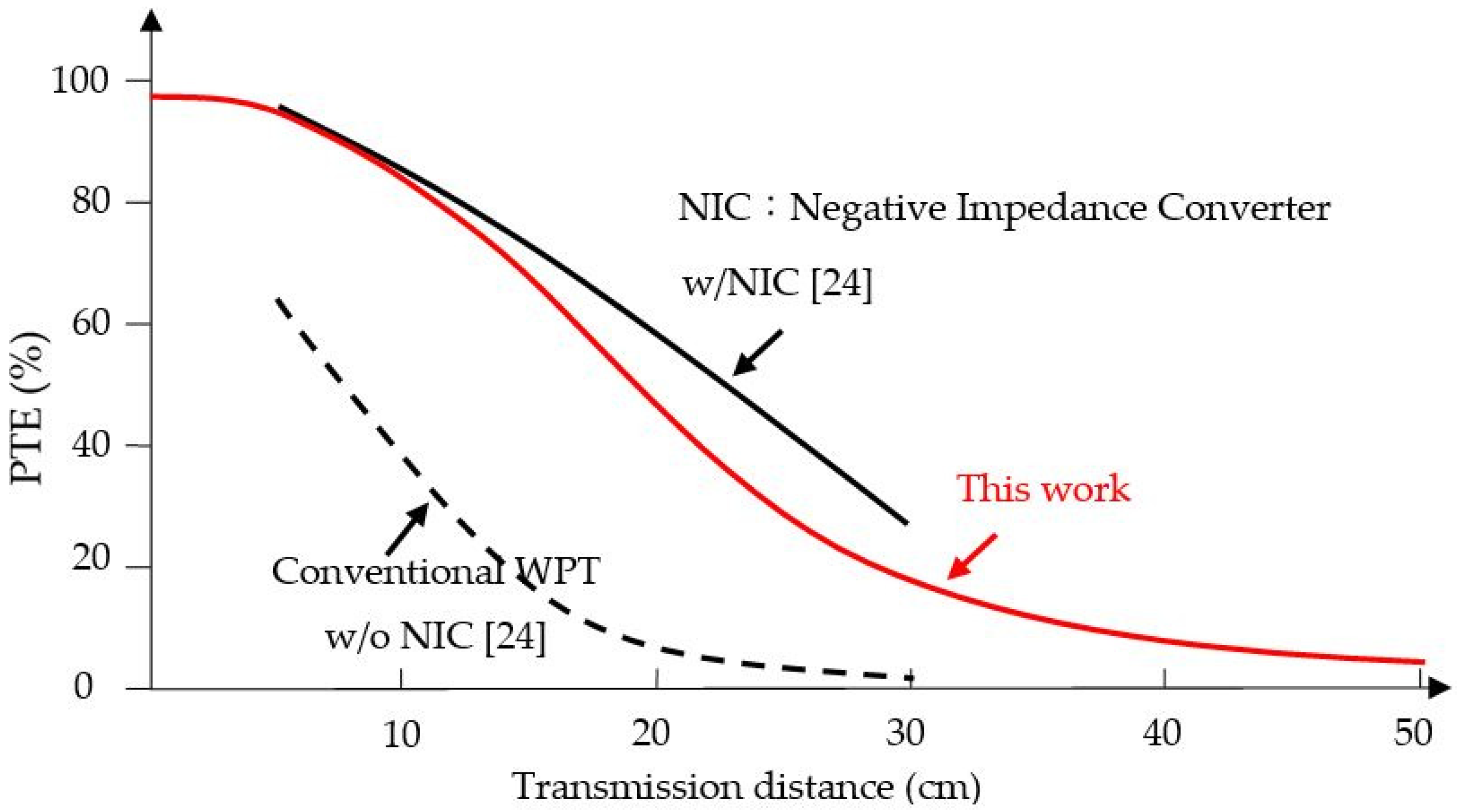
As shown in Figure 16, a single PTU for the resonant WPT based on the D-mode GaN HEMT class-E amplifier was capable of transferring 1 W of power to a PRU 140 cm away. In the experiment, the load comprised 44 LEDs in series, each of which had a nominal power of 0.06 W. The maximum voltage VDS,max was 700 V, and the maximum current iD was 2.5 A. The radii of the coils for both PTU and PRU were approximately 25 cm. When the PRU was 50 cm from the PTU, the PRU received 5 W power from the PTU (Figure 17). Due to the different distances between the PTU and PRUs in the WPT application, the maximum voltage VDS,max, which is proportional to the duty cycle δ, must be adjusted to send power at an optimal efficiency. The minimum power input control was applied for this purpose according to the look-up table. The maximum voltage VDS,max is typically triple the input voltage VDD in practice. Hence, the breakdown voltage of the D-mode GaN HEMT had to be higher than 1000 V for the application of 220 VAC, which was rectified to 310 VDC. Figure 18 shows the performance comparison of the PTE (%) in terms of transmission distance (cm). The method proposed in this paper yields performance comparable to the WPT with NIC method [24] with, however, no additional impedance transformation network circuit.
4. Conclusions
The D-mode GaN HEMT fabricated at the authors’ university, the National Chiao Tung University, was successfully implemented into the class-E amplifier circuit. The design of the D-mode GaN HEMT gate drive for the wireless power transfer is sensitive to parameters including the gate-drain parasitic capacitance Crss (=CGD) and the gate input parasitic capacitance Ciss (=CGD + CGS). These parasitic capacitances of the GaN HEMT are essential for higher frequency switching with low switching loss. In the circuit design aimed at achieving the maximum power transfer, the corresponding impedance matching control was obtained in this research via adjustment of the resonant frequency ωo,. Nevertheless, by controlling the duty ratio δ, a minimum power input control that trades off the power delivered to load for the switching loss of the GaN HEMT was obtained and found to yield good power transfer efficiency. The resulting resonant WPT was capable of transferring 1 W over the 140 cm distance between the PTU and PRU. Our minimum power input control is an empirical method that generates a look-up table to optimize efficiency in WPT applications. In the future, the proposed design will be implemented for multiple-input and multiple-output (MIMO) applications—i.e., multiple PTUs serving multiple PRUs, which need to obtain the proper optimization method from among their individual look-up tables—via a 2.4 GHz communication network (recommended by the Airfuel Alliance) in order to improve the efficiency of power transfer.
Author Contributions
Conceptualization, E.Y.C. and W.-H.C.; methodology, Y.-C.W.; software, C.-C.W.; validation, Y.-C.W., C.-C.W.; formal analysis, Y.-C.W.; resources, Y.-C.W.; writing—original draft preparation, W.-H.C.; writing—review and editing, C.-C.W.; visualization, E.Y.C.; supervision, E.Y.C.; project administration, E.Y.C.; funding acquisition, W.-H.C. All authors have read and agreed to the published version of the manuscript.
Funding
This research was funded by the Ministry of Science and Technology, R.O.C, grant number MOST(NSC)109-3116-F009-001-CC1.
Institutional Review Board Statement
Not applicable.
Informed Consent Statement
Not applicable.
Data Availability Statement
Data sharing is not applicable.
Acknowledgments
This work was supported by the Ministry of Science and Technology, R.O.C. The authors would also like to thank CSD Lab for the fabrication of D-Mode MIS-HEMT chips, and IM Lab graduate students Ching-Yao Liu, Guo-Bin Wang, and Yue-Cong Sie for their help in the experiment setup.
Conflicts of Interest
The authors declare no conflict of interest.
References
- Sokal, N.O.; Sokal, A.D. Class E—A new class of high-efficiency tuned single-ended switching power amplifiers. IEEE J. Solid State Circuits 1975, SSC-10, 168–176. [Google Scholar] [CrossRef]
- Liu, M.; Zhao, C.; Song, J.; Ma, C. Battery Charging Profile-Based Parameter Design of a 6.78-MHz Class E2 Wireless Charging System. IEEE Trans. Ind. Electron. 2017, 64, 6169–6178. [Google Scholar] [CrossRef]
- Aldhaher, S.; Mitcheson, P.D.; Arteaga, J.M.; Kkelis, G.; Yates, D.C. Light-weight wireless power transfer for mid-air charging of drones. In Proceedings of the 2017 11th European Conference on Antennas and Propagation (EUCAP), Paris, France, 19–24 March; pp. 336–340.
- Chen, W.T.; Chinga, R.A.; Yoshida, S.; Lin, J.; Hsu, C.K. A 36 W wireless power transfer system with 82% efficiency for LED lighting applications. Trans. Jpn. Inst. Electron. Packag. 2013, 6, 32–37. [Google Scholar] [CrossRef] [Green Version]
- Chokkalingam, B.; Padmanaban, S.; Leonowicz, Z.M. Class E power amplifier design and optimization for the capacitive coupled wireless power transfer system in biomedical implants. Energies 2017, 10, 1409. [Google Scholar]
- Paolucci, M.; Green, P.B. Benefits of GaN e-Mode HEMTs in Wireless Power Transfer—GaN Power Devices in Resonant Class D and Class E Radio Frequency Power Amplifiers. October 2018. Rev 1.0. Infineon, White Paper. Available online: https://www.infineon.com/wirelesscharging (accessed on 17 October 2018).
- Green, P.B. Class-E Power Amplifier Design for Wireless Power Transfer. August 2018. Rev 1.2. Infineon, Appl. Note 1803. pp. 1–51. Available online: https://www.infineon.com/wirelesscharging (accessed on 10 August 2018).
- Akuzawa, Y.; Ito, Y.; Ezoe, T.; Sakai, K. A 99%-efficiency GaN converter for 6.78 MHz magnetic resonant wireless power transfer system. J. Eng. 2014, 10, 598–600. [Google Scholar] [CrossRef]
- Lee, S.H.; Yi, K.P.; Kim, M.Y. 6.78-MHz, 50-W wireless power supply over a 60-cm distance using a GaN-based full-bridge inverter. Energies 2019, 12, 371. [Google Scholar] [CrossRef] [Green Version]
- Yeh, C.H.; Lin, Y.T.; Kuo, C.C.; Huang, C.J.; Xie, C.Y.; Lu, S.F.; Yang, W.H.; Chen, K.H.; Lin, Y.H. A 70W and 90% GaN-based class-E wireless-power-transfer system with automatic-matching-point-search control for zero-voltage switching and zero-voltage-derivative switching. In Proceedings of the 2018 IEEE International Solid-State Circuits Conference-(ISSCC), San Francisco, CA, USA, 11–15 February 2018; pp. 138–140. [Google Scholar]
- Xie, C.Y.; Yang, S.H.; Lu, S.F.; Lin, F.Y.; Lin, Y.A.; Ou-Yang, Y.Z.; Chen, K.H.; Liu, K.C.; Lin, Y.H. 15.3 A 100W and 91% GaN-Based Class-E Wireless-Power-Transfer Transmitter with Differential-Impedance-Matching Control for Charging Multiple Devices. In Proceedings of the 2019 IEEE International Solid-State Circuits Conference-(ISSCC), San Francisco, CA, USA, 17–21 February 2019; pp. 242–244. [Google Scholar]
- Grebennikov, A. Load Network Design Techniques for Class E RF and Microwave Amplifier. High Freq. Electron. 2004, 3, 18–32. [Google Scholar]
- Barman, S.D.; Reza, A.W.; Kumar, N. Coupling Tuning Based Impedance Matching for Maximum Wireless Power Transfer Efficiency. J. Comput. Sci. Comput. Math. 2016, 6. [Google Scholar] [CrossRef]
- Jiang, C.; Chau, K.T.; Liu, C.; Lee, C.H. An overview of resonant circuits for wireless power transfer. Energies 2017, 10, 894. [Google Scholar] [CrossRef]
- Muharam, A.; Ahmad, S.; Hattori, R. Scaling-Factor and Design Guidelines for Shielded-Capacitive Power Transfer. Energies 2020, 13, 4240. [Google Scholar] [CrossRef]
- Minnaert, B.; Costanzo, A.; Monti, G.; Mongiardo, M. Capacitive Wireless Power Transfer with Multiple Transmitters: Efficiency Optimization. Energies 2020, 13, 3482. [Google Scholar] [CrossRef]
- Li, C.; Wang, B.; Huang, R.; Yi, Y. A Resonant Coupling Power Transfer System Using Two Driving Coils. Energies 2019, 12, 2914. [Google Scholar] [CrossRef] [Green Version]
- Wen, F.; Li, R. Parameter Analysis and Optimization of Class-E Power Amplifier Used in Wireless Power Transfer System. Energies 2019, 12, 3240. [Google Scholar] [CrossRef] [Green Version]
- Ng, W.T.; Yu, J.; Wang, M.; Li, R.; Zhang, W. Design Trends in Smart Gate Driver ICs for Power GaN HEMTs. In Proceedings of the 2018 14th IEEE International Conference on Solid-State and Integrated Circuit Technology (ICSICT), Qingdao, China, 31 October–3 November 2018; pp. 1–4. [Google Scholar]
- Ishibashi, T.; Okamoto, M.; Hiraki, E.; Tanaka, T.; Hashizume, T.; Kikuta, D.; Kachi, T. Experimental validation of normally-on GaN HEMT and its gate drive circuit. IEEE Trans. Ind. Appl. 2014, 51, 2415–2422. [Google Scholar] [CrossRef]
- Chou, P.C.; Cheng, S. Performance characterization of gallium nitride HEMT cascode switch for power conditioning applications. Mater. Sci. Eng. B Adv. 2015, 198, 43–50. [Google Scholar] [CrossRef]
- Wu, C.C.; Jeng, S.L. Simulation Model Development for Packaged Cascode Gallium Nitride Field-Effect Transistors. Crystals 2017, 7, 250. [Google Scholar] [CrossRef] [Green Version]
- Liu, C.Y.; Wang, G.B.; Wu, C.C.; Chang, E.Y.; Cheng, S.; Chieng, W.-H. Derivation of the Resonance Mechanism for Wireless Power Transfer Using Class-E Amplifier. Energies 2021, 14, 632. [Google Scholar] [CrossRef]
- Kim, T.-H.; Yun, G.-H.; Lee, W.; Yook, J.-G. Highly efficient WPT system with negative impedance converter for Q-factor improvement. IEEE Access 2019, 7, 108750–108760. [Google Scholar]
- Liu, S.; Liu, M.; Fu, M.; Ma, C.; Zhu, X. A high-efficiency Class-E power amplifier with wide-range load in WPT systems. In Proceedings of the 2015 IEEE Wireless Power Transfer Conference (WPTC), Boulder, CO, USA, 13–15 May 2015; pp. 1–3. [Google Scholar] [CrossRef]
Figure 1.
Flowchart of key characteristic parameters, which may also refer to [23], for achieving the minimum power input control.
Figure 1.
Flowchart of key characteristic parameters, which may also refer to [23], for achieving the minimum power input control.
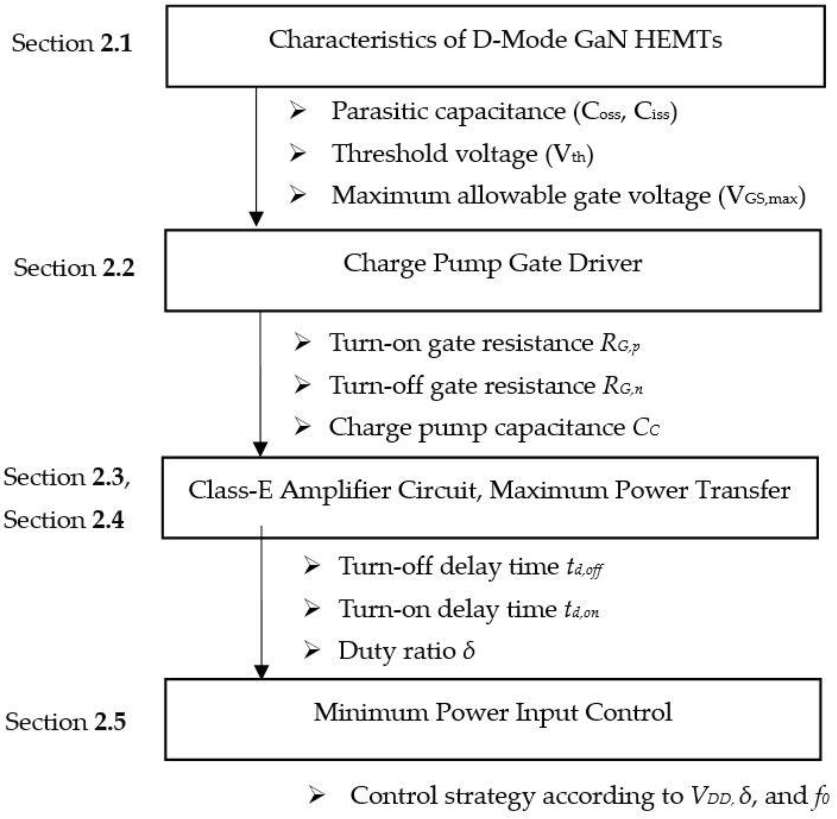
Figure 2.
Characteristics of the D-mode GaN HEMT: (a) transfer characteristic; (b) output characteristic.
Figure 2.
Characteristics of the D-mode GaN HEMT: (a) transfer characteristic; (b) output characteristic.

Figure 3.
The parasitic capacitance of D-mode GaN HEMT via (a) TO220 and (b) TO247 packaging.

Figure 4.
Charge pump gate drive design.
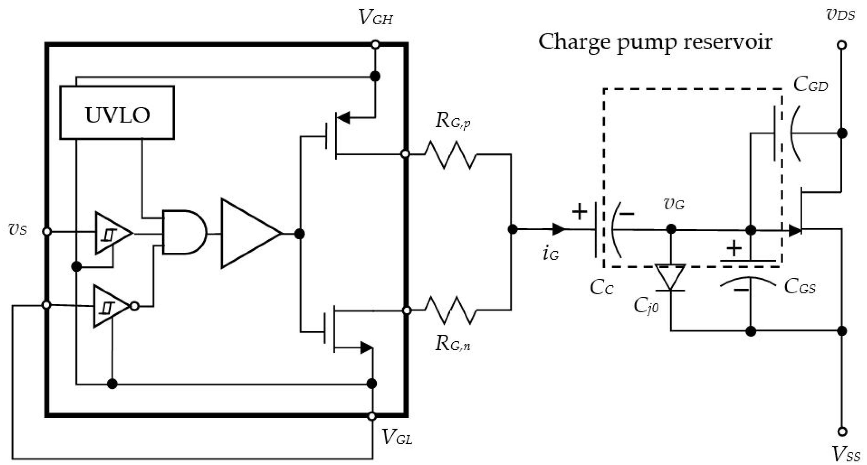
Figure 5.
Gate response with high voltage vDS effect from class-E amplifier.

Figure 6.
Class-E amplifier.
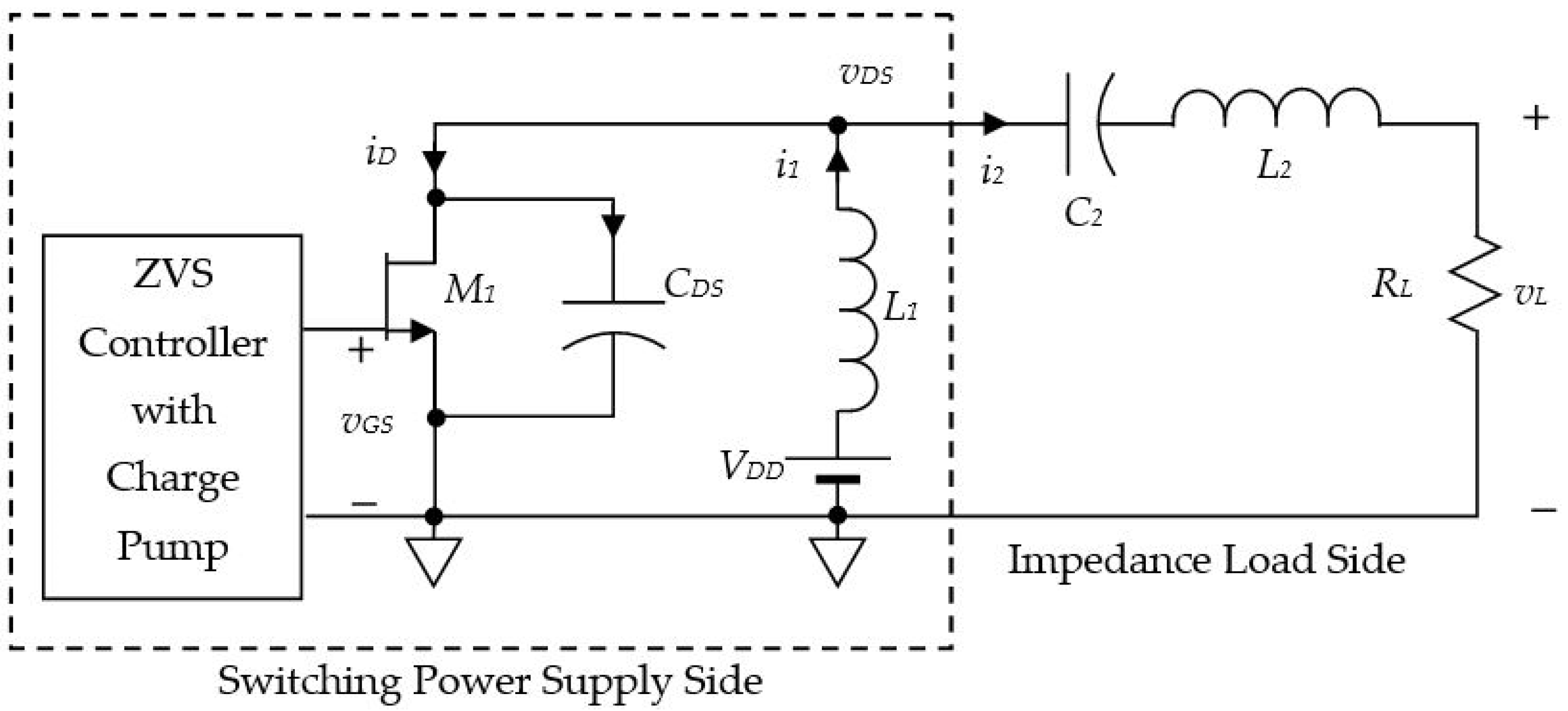
Figure 7.
(a) WPT experimental layout; (b) charge pump gate driver for D-mode GaN HEMT.
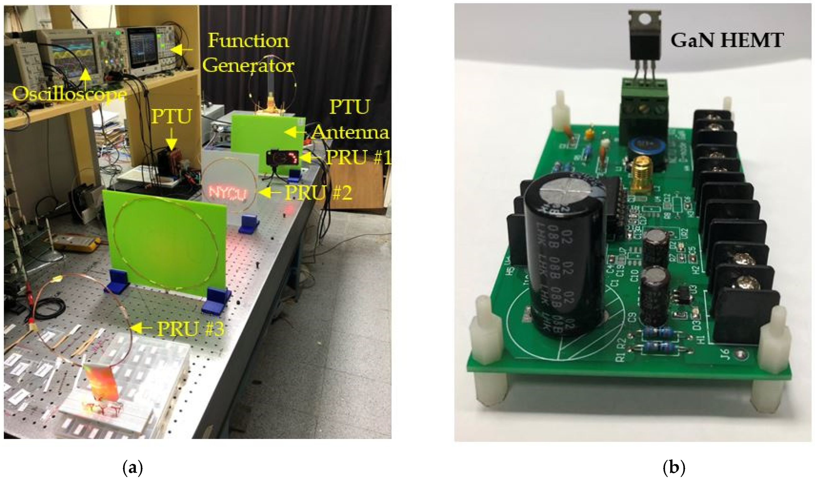
Figure 8.
(a) PWM control of D-mode GaN HEMT; (b) SPICE analysis.

Figure 9.
Example of (a) i2 current form. (b) SPICE analysis.

Figure 10.
The comparison of the gate driver input (dotted line) and actual gate-source voltage output (solid line).
Figure 10.
The comparison of the gate driver input (dotted line) and actual gate-source voltage output (solid line).

Figure 11.
Wireless power transfer equivalent circuit.

Figure 12.
VDS,max vs. duty ratio.
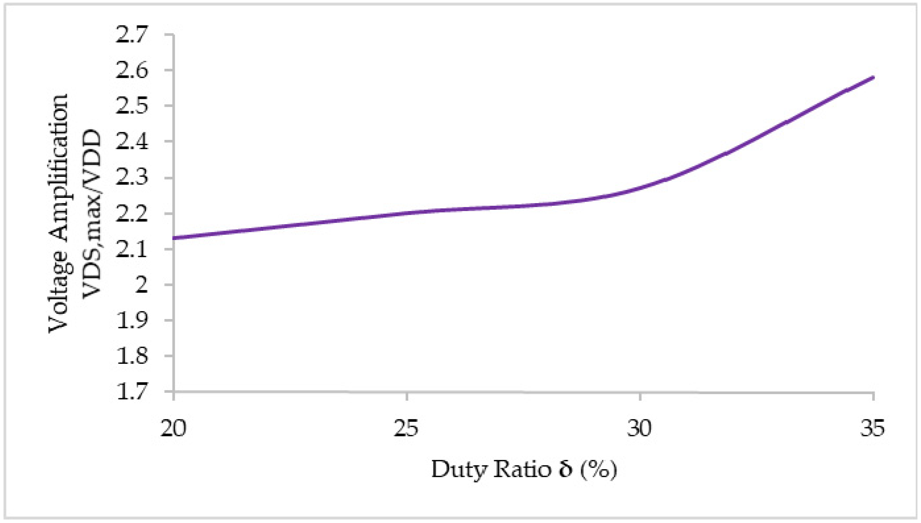
Figure 13.
Input power due to different resonant frequencies f0 and duty ratios δ% for VDD = 108 V.

Figure 14.
Minimum power input vs. the duty ratio δ%.

Figure 15.
Resonant frequency f0 vs. the duty ratio δ% under the minimum power input control.
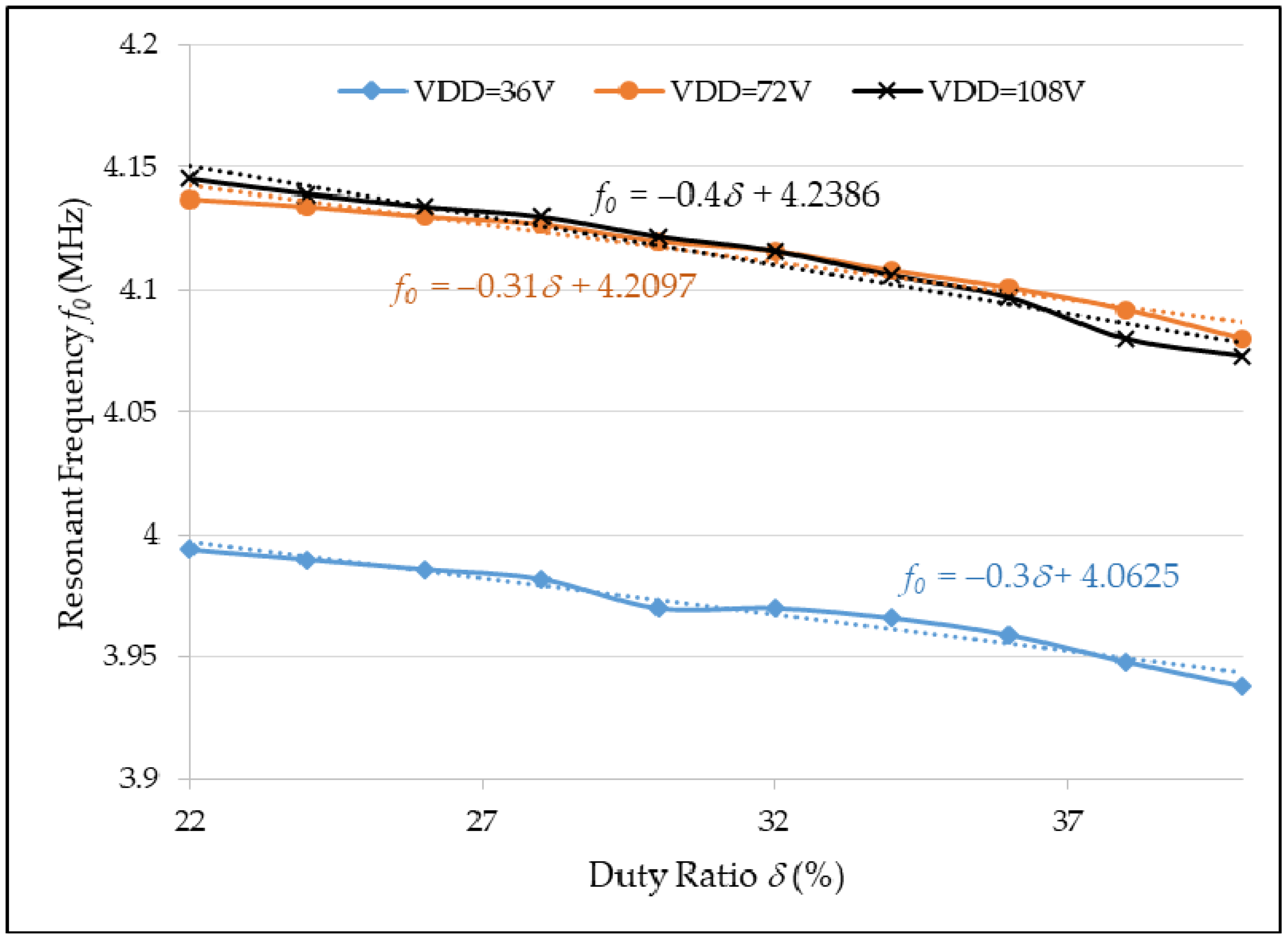
Figure 16.
Data log of the class-E amplifier at 40 W at VDD = 262 V.

Figure 17.
Example of 5 W at a 50 cm distance between the PTU and PRU.

Figure 18.
The performance comparison of the PTE (%) vs. transmission distance (cm).

Table 1.
Summary of characteristics of the D-mode GaN HEMT.
| Symbol | Parameter | Value | Unit |
|---|---|---|---|
| vGS,ON | Turn-on voltage | −7 | V |
| CDS | Drain-source parasitic capacitance | 100 | pF |
| CGD | Gate drain Parasitic capacitance | 80 | pF |
| CGS | Gate source Parasitic capacitance | 420 | pF |
| VGS,max | Maximum gate-source voltage | 8 | V |
| VDS,BD | Drain-source breakdown voltage | 1000 | V |
| id,max | Maximum drain current | 35 | A |
Table 2.
The parasitic capacitances of the D-mode GaN HEMT.
| Symbol | Parameter | Typical (pf) | Conditions |
|---|---|---|---|
| Ciss | Input capacitance | 99.7 | VDS = 150 V, VG = −10 V, T = 25 °C, 1 MHz |
| Coss | Output capacitance | 9.2 | |
| Crss | Transfer capacitance | 7.1 |
Table 3.
Parameters used in the charge pump gate drive.
| Symbol | Parameter | Value | Unit |
|---|---|---|---|
| RG,p | Turn-on gate resistance | 12 | Ω |
| RG,n | Turn-off gate resistance | 30 | Ω |
| CC | Charge pump capacitance | 5 | nF |
| CGS | Diode capacitance | 40 | pF |
| IR | Diode reverse saturation current | 50 | µA |
Table 4.
Class-E amplifier equivalent parameters.
| Symbol | Unit | Value |
|---|---|---|
| RL | kΩ | 5 1 |
| CDS | pF | 100 |
| C2 | pF | 75 |
| L1 | µH | 47 |
| L2 | µH | 8 |
1 Equivalent.
Publisher’s Note: MDPI stays neutral with regard to jurisdictional claims in published maps and institutional affiliations. |
© 2021 by the authors. Licensee MDPI, Basel, Switzerland. This article is an open access article distributed under the terms and conditions of the Creative Commons Attribution (CC BY) license (https://creativecommons.org/licenses/by/4.0/).
Share and Cite
MDPI and ACS Style
Weng, Y.-C.; Wu, C.-C.; Chang, E.Y.; Chieng, W.-H. Minimum Power Input Control for Class-E Amplifier Using Depletion-Mode Gallium Nitride High Electron Mobility Transistor. Energies 2021, 14, 2302. https://doi.org/10.3390/en14082302
AMA Style
Weng Y-C, Wu C-C, Chang EY, Chieng W-H. Minimum Power Input Control for Class-E Amplifier Using Depletion-Mode Gallium Nitride High Electron Mobility Transistor. Energies. 2021; 14(8):2302. https://doi.org/10.3390/en14082302
Chicago/Turabian StyleWeng, You-Chen, Chih-Chiang Wu, Edward Yi Chang, and Wei-Hua Chieng. 2021. "Minimum Power Input Control for Class-E Amplifier Using Depletion-Mode Gallium Nitride High Electron Mobility Transistor" Energies 14, no. 8: 2302. https://doi.org/10.3390/en14082302
Note that from the first issue of 2016, this journal uses article numbers instead of page numbers. See further details here.