Carrier-Phase-Shifted Rotation Pulse-Width-Modulation Scheme for Dynamic Active Power Balance of Modules in Cascaded H-Bridge STATCOMs


1
State Key Laboratory of Advanced Electromagnetic Engineering and Technology, School of Electrical and Electronic Engineering, Huazhong University of Science and Technology, Wuhan 430074, China
2
State Grid Jingzhou City Jingzhou District Power Supply Company, Jingzhou 434100, China
*
Author to whom correspondence should be addressed.
Energies 2020, 13(5), 1052; https://doi.org/10.3390/en13051052
Submission received: 4 February 2020
/
Revised: 22 February 2020
/
Accepted: 24 February 2020
/
Published: 26 February 2020
(This article belongs to the Special Issue Multilevel Power Converters Control and Modulation Techniques)
Abstract
:In the medium-voltage power distribution system, cascaded H-bridge (CHB) static synchronous compensators (STATCOMs) are widely utilized to solve power quality issues by injecting the controlled reactive current into the system. The carrier-phase-shifted (CPS) pulse-width-modulation (PWM) scheme is preferred for CHB-STATCOMs, because it can minimize the compensating current distortion and realize the relative active power balance among the H-bridge modules. This paper reveals the influence of the carrier phase difference on the module active power balance, and proposes a carrier rotation technique with a CPS-PWM scheme to address this drawback. The rotation rules were analyzed, and the rotation time was especially designed to enhance the robustness of the system. With the proposed method, the natural dynamic active power balance of each module could be achieved, and the capacitor voltage could maintain balance without the individual capacitor voltage control or the auxiliary circuits in theory. The experimental results acquired from a downscaled CHB-STATCOM prototype demonstrated the feasibility of the proposed CPS rotation PWM scheme.
1. Introduction
With the increase in various renewable energy sources and power electronic devices connected to the microgrid or power distribution systems, power quality problems, such as voltage fluctuation at the point of common coupling (PCC), harmonic pollution, uncontrolled reactive power, and poor power factor become more serious [1,2].
A fixed capacitor bank in parallel to the power system is an old technology to manage the system reactive power [3]. However, its compensation range is discontinuous and the dynamic response is very low. With the development of semiconductor technologies, the thyristor-controlled static var compensators (SVC) appeared in the late 1970s [4]. Then, the flexible AC transmission system (FACTS) equipment based on fully controlled devices, e.g., insulated gate bipolar transistor (IGBT), began to take the place of the thyristor-controlled SVC, benefiting from a larger compensation range, a higher switching frequency, a lower harmonic injection, and a faster dynamic response [5]. Static synchronous compensators (STATCOMs) are the major FACTS equipment. Its mode is designed to dynamically adjust the reactive power of the AC microgrid [6], is controlled as a voltage source and injects capacitive or inductive reactive current into the system, which is helpful for PCC voltage regulation, power factor correction, transient stability improvement, and system oscillation suppression [7,8].
In order to accommodate to the high voltage and large capacity requirements in modern power distribution or transmission system, multi-pulse and multilevel circuit became the major choices for STATCOM [9,10,11,12,13,14,15,16]. The multi-pulse STATCOM utilizes a zigzag transformer connected to the utility line. There are obvious disadvantages, such as high cost, large volume, and high power losses. Moreover, the transformer saturation effect might create difficulties for designing the control system [9]. As for multilevel STATCOMs, the device or module cascaded topology replaces the function of the transformer, and the above side-effects are greatly avoided. A three-level diode-clamped multilevel converter was introduced in [10] and it has been expanded to more than four-levels, since its appearance [11]. However, the number of clamping diodes and the severe problems with DC-link voltage control restrict the further expansion of the voltage levels. A flying capacitor-clamped multilevel converter was first proposed as a chopper in [12]. For this topology, the clamping capacitors voltages were automatically balanced when an adequate modulation scheme was implemented. However, when the switching frequency was low, the capacitances became large for maintaining the voltages within the switching period [13]. A cascaded H-bridge (CHB) converter with a star connection first appeared in [14], which omitted the clamping components. Its delta-connection configuration was presented in [15], and the three-phase independent control enhanced the system reliability. Due to the high efficiency, excellent output current characteristics, high modularity and scalability, CHB has become the most preferred choice for the STATCOM project installation, till date [16].
In a single phase of a CHB-STATCOM, the AC-sides of the H-bridge modules are connected in series, and the cascaded phase voltage are synthesized by the AC-side output voltage of each module. Therefore, it is important to maintain the DC-side capacitor voltage balance of the modules for its safe operation. The multi-carrier, pulse-width-modulation (PWM) modulation methods, e.g., carrier-phase-shifted (CPS) and carrier-phase-disposition (CPD), are commonly recommended for CHB-STATCOMs [17,18]. With an appropriate carrier allocation for each module, some switching harmonics can be canceled out in the cascaded voltage, and the equivalent switching frequency can be increased, which would contribute to the voltage and current waveforms with good quality. Considering the consistence of each module, the CPS method is preferred, where the switching frequencies for the modules are identical. It realizes the relative active power balance among the modules neglecting the carrier phase differences [19]. The asymmetrical CPS–PWM method was proposed to improve the switching harmonic performance of the partly regenerative converter by eliminating low-frequency switching harmonics [20], and the fundamental component in the AC-side voltage of the module is regarded as the same as that of the voltage reference in the PWM process. The carrier phase would also affect the fundamental component, especially when the carrier frequency is relatively low. Thus, if the minor carrier phase differences among the modules are taken into consideration, the active power of the modules would be slightly different and the capacitor voltages would diverge from the rated value without any limitation. In the end, with an increasing degree of imbalanced capacitor voltages, the fault current would trigger the protection system and the converter would stop working.
There are two main technical routes to overcome the different active power of the modules and maintain the capacitor voltage balance for CHB-STATCOMs. On the one hand, [21,22] introduced the external balance circuits to realize the active power exchanges among different modules. Nevertheless, they increased the cost and complexity of the systems. On the other hand, some additional close-loop active power control strategies were proposed for an individual module [23,24,25]. These methods changed the voltage reference to achieve the balance, but increased the complexity of the control system. None of the above methods solved the problem of active power imbalance caused by the carrier difference in the modulation process and realized the complete natural active power balance for the modules.
In this paper, the influence of the carrier phase difference on the module active power balance is revealed, and a CPS rotation (CPSR) PWM scheme is proposed to overcome this drawback. The rotation time is designed to enhance the robustness of the system and its realization is illustrated. With the proposed method, the natural dynamic active power balance for the modules can be realized.
The outline of the remaining part is organized as follows. Section 2 introduces the basic control method for CHB-STATCOMs. Section 3 describes the conventional CPS-PWM method and analyzes the influence of the carrier phase difference on the module active power balance. Section 4 proposes the CPSR scheme and explains the rotation rules to enhance the system robustness. Section 5 shows the experimental verification. Finally, Section 6 concludes the whole paper.
2. Basic Control Method for CHB-STATCOM
A three-phase CHB-STATCOM with a star configuration is illustrated in the left part of Figure 1. One phase of the STATCOM comprises N CHB modules and a buffer inductor L in series. ix represents the three-phase compensating reactive current of the STATCOM and vx represents the three-phase grid voltage, where x = a, b, c. The positive direction of the compensating current is defined from the grid to the converter. Therefore, if it leads the grid voltage by 90 degrees, the converter works in the capacitive mode and injects inductive reactive current to the grid. Contrarily, the converter works in the inductive mode and injects capacitive reactive current to the grid with the compensating current lagging the grid voltage by 90 degrees.
Its classical voltage and current dual-loop control is illustrated in the right part of Figure 1. The external voltage loop ensures the feedback average capacitor voltage, UC_ave, and tracks the capacitor voltage reference UC_ref. It can be regarded as the entire active power control for the converter. The inner current loop based on the d-q coordinates makes the compensation current track the current reference Iq_ref with zero error [26], where ωt represents the phase-locked-loop message. The d-q decoupling skill in the inner current loop can speed up the transient regulation of the controller [27]. The grid voltage feedforward loop enhances the system stability and avoids the interference of the grid voltages [28]. The final voltage reverence vx_ref is given to the modules per phase to generate the drive pulses through their PWM processes.
3. CPS-PWM Method and Carrier Phase Difference Influence on Module Active Power Balance
3.1. Conventional CPS-PWM Method
A unipolar double-frequency modulation rule [29] is chosen for the PWM process in this paper, which is shown in Figure 2. During the voltage reference vx_ref is positive, if the carrier is between vx_ref and −vx_ref in the blue area of Figure 2, the H-bridge module outputs positive voltage level UC. Otherwise, it outputs zero voltage level. During the voltage reference, vx_ref is negative if the carrier is between vx_ref and -vx_ref in the red area of Figure 2, and the H-bridge module outputs negative voltage level -UC. Otherwise, it outputs zero voltage level.
With the double-Fourier analysis tool [30], the components with the different frequencies in the output voltage of the H-bridge module can be decomposed as (1).
where the initial phase angles for the voltage reference and carrier are set to be 0 and αc, respectively. M is the modulation index. ωs is the fundamental angular frequency of the voltage reference and ωc is the angular frequency of the carrier. Jn(x) is the Bessel function [31].
Equation (1) indicates that, the output voltage of a single H-bridge module contains a fundamental component, and sideband harmonic components whose frequencies are around the even multiples of the fundamental frequency. The switching frequency is the double of the carrier frequency.
Assume that N H-bridge modules are connected in series with constant capacitor voltage UC, and the carriers for the modules have π/N phase shifters, the cascaded output voltage F(t) can be obtained as
Taking N = 3 as an example, Figure 3 shows the vector graphs for the sideband harmonic components for these three modules. When m ≠ 6k, where k is a positive integer, the sideband harmonics evenly distribute in the space as shown in Figure 3a, and they would not contribute to the cascaded output voltage. When m = 6k, the amplitudes and phase angles of the sideband harmonics are the same for the three modules, as shown in Figure 3b, therefore, they would triple in the cascaded output voltage. When N is another positive integer, similar conclusions can be drawn.
Therefore, Equation (2) is simplified as
Equation (3) indicates that, with the CPS-PWM method, the cascaded output voltage of N H-bridge modules comprise a fundamental component, and sideband harmonic components whose frequencies are around the 2N multiples of the fundamental frequency. Therefore, the equivalent switching frequency raises to 2N times of the carrier frequency.
It should be noted that, in this case, the phase shifter is π/N, and it is suitable, irrespective of whether N is odd or even. However, if the phase shifter is π/2N, this effectiveness can only be realized when N is an odd.
3.2. Carrier Phase Difference Influence on Module Active Power Balance
Ignoring the power losses of the CHB-STATCOM, and assuming the capacitor voltages of the modules are balanced, the vector graphs for the fundamental current and voltages in the CHB-STATCOM are shown in Figure 4, in the case of N = 3. The output voltages of these three modules are defined as f1, f2, and f3, respectively. The grid voltage and voltage on the buffer inductor are determined as v and vL, respectively; i is the current in this loop, and their specified positive directions have been given. As shown in the right part of Figure 4, f1, f2, and f3 have the same phase angles with the gird voltage v, but the phase angle of the inductor voltage vL is the opposite. Thus, the current i leads vL by 90 degrees, but lags v by 90 degrees. Therefore, in this circumstance, the converter works in the inductive mode. As for the modules, because the vectors of the output voltages f1, f2, and f3 are vertical to that of the current i, there is no active power flowing into the module, which ensures the capacitor voltage to keep balance in this ideal state. Considering the power losses, the external voltage loop shown in Figure 1 can manage the entire power losses of the converter.
From the module output voltage expression shown as Equation (1), the fundamental component is revealed in the first term, and the sideband harmonics are revealed in the second term. However, the sideband harmonic clusters would affect the fundamental component with the following prerequisite.
Defining the carrier ratio ωc/ωs = K, Equation (4) is simplified as
Substituting Equations (4) and (5) into Equation (1), the fundamental component resulting from the sideband harmonics is calculated as
The Bessel function has the following characteristics [31],
Thus, Equation (6) can be rewritten as
Seeing Figure 5, the envelop of the Bessel function curves will converge to the zero axis with the increasing order (mK-1). Moreover, 1/m appears in the coefficient, which is inversely proportional to m. Therefore, in the following analysis, only m = 2 is considered considering the minimum (mK-1) and maximum 1/m. With this assumption, Equation (8) is further derived as Equation (9).
The carrier phase difference will lead to different initial carrier phase angle αc for each module. Still taking the module number N = 3 as an example, the initial carrier phase angles for these modules are 0, π/3, and 2π/3. Thus, the fundamental components resulting from the sideband harmonics for each module are listed as,
where
These components are in positive sequence with the same amplitude –A, and their amplitude is influenced by the carrier ratio K and modulation index M with fixed UC. In Figure 6, the relationship of (–A/UC) with varied carrier ratio K and modulation index M is interpreted. In a fixed modulation index M, with smaller K, (–A/UC) is larger. It indicates that, the carrier phase differences for the modules will lead to different fundamental components in the output voltage. This effect would be more obvious when the carrier ratio is relatively low.
Taking this additional fundamental component into consideration, Figure 7 redraws the vector graphs for the modules. The black vector arrows show the synthesized fundamental component in the output voltage of the modules. Obviously, the voltages are not vertical to the current for the second and third modules, and it would inject the active power to the module or absorb the active power from the module. The capacitor voltages cannot maintain balance in this case.
Although the additional fundamental component is relatively small compared with the initial part shown in the first term in Equation (1), the active power injecting or absorbing phenomena are irreversible during the CHB-STATCOM working period, and the capacitor voltages will diverge from the rated value continually until it crashes the system in the end.
4. Proposed CPSR-PWM Scheme
In order to eliminate the unequal active power caused by the carrier phase difference in the modulation process, the carrier of each module can rotate repeatedly after a period of time. At the same time, in order to maintain the good harmonic characteristics of the cascaded output voltage, this rotation must be carried out organically among the modules. The following section analyzes this rotation scheme when the module number, N = 3, carrier ratio K = 2, and modulation index M = 5/6.
As shown in Figure 8, in the modulation process of these three modules, the period of the carrier rotation is that of voltage reference, and this rotation is completed within the three reference periods. It can be seen from the seven-level cascade output voltage that, the output voltage waveform is not affected by the carrier rotation and maintains the original good harmonic performance.
The active power of each module keeps dynamic balance in these periods. In order to achieve this dynamic balance, the carrier rotation period for each module must be an integral multiple of the voltage reference period, and the rotation time should be synchronous for all modules. Otherwise, the harmonic phase relationship shown in Figure 3 will not exist, which will inevitably affect the quality of output voltage and current.
In Figure 8, the carrier rotation time is at the reference zero-crossing point. However, in Figure 9, the rotation happens at the reference non-zero-crossing point. As long as the rotation period is an integral multiple of the reference period, and the rotation actions are carried out simultaneously for all modules, the good harmonic performance of the cascaded voltage can be achieved and the active power of a single module can also be dynamically balanced.
In the physical implementation of the proposed CPSR-PWM scheme, synchronous rotation actions for all modules might not be fully guaranteed because of the signal transmission delays or errors. In order to enhance the system robustness, the rotation time should be designed reasonably to minimize the influence of the asynchronous rotation on the cascaded output voltage characteristics.
It is supposed that, the rotation time has a 30-degree difference relative to the carrier period for the three modules, and Figure 10; Figure 11 illustrate the modulation processes and waveforms of the cascaded output voltages with zero-crossing rotation and non-zero-crossing rotation. Table 1 concludes the total harmonics distortions (THDs) in these two situations. In the given three reference periods, the THDs of the cascaded output voltage in the zero-crossing rotation are lower than those in the non-zero-crossing rotation, whether in a single period or the whole periods.
We define the asynchronous rotation moments in Figure 10 and Figure 11 as 0 and 90 degrees, with respect to the reference. In Figure 12, the average THDs of the cascaded output voltage with rotation time varying in half reference period are concluded. Obviously, the rotation time should be at the reference zero-crossing point to achieve the best robustness of the system.
With different carrier ratio K = 4, Figure 13 gives the THDs of the cascaded output voltage with rotation time varying in half reference period. For three modules, there is still a 30-degree difference relative to the carrier period with a synchronous rotation. The result reveals a similar conclusion. That is, the lowest THD is obtained at the reference zero-crossing point. It can be expected that, although the THDs decrease with increasing carrier ratio K, the best performance of the cascaded output voltage keeps at the reference zero-crossing point.
5. Experimental Verification
In order to demonstrate the feasibility and advantage of the proposed CPRS-PWM scheme for CHB-STATCOMs, experimental verifications are carried out on an experimental prototype, whose H-bridge module are shown in Figure 14.
This prototype is based on a multi-digital signal processor (DSP, TMS32028335) hierarchical control system [32]. The master DSP samples the necessary quantities, such as grid voltages, capacitor voltages, compensating currents, and executes the dual-loop control programmer, then transmits the calculated voltage reference to the slave DSPs in the modules, using serial peripheral interface (SPI) communication. Simultaneously, the carrier synchronization signal generated by the master DSP is captured by all slave DSPs. The proposed CPSR-PWM scheme is implemented in the slave DSPs and the pulses are generated to drive the IGBTs. The system parameters are listed in Table 2.
Figure 15 gives the experimental waveforms of the capacitor voltages, the grid voltage, and the compensating current. At t = 0, the capacitor voltages are about 33 V under the uncontrolled rectifier state. At t = 1 s, the capacitor voltages are set to be boosted to the rated value 48 V, with the help of the outer voltage loop. However, with the conventional CPS-PWM scheme, the voltages diverge from the rated value due to the unbalanced active power among the modules resulting from the carrier phase differences shown in Figure 15(a1). At t = 3 s, a capacitive reactive current command 5 A is given in the inner current loop. Unfortunately, the compensating current shown in Figure 15(b1) has a severe distortion, whose THD is 67.027% and Figure 15(c1) draws its harmonic spectra.
With the proposed CPSR-PWM method shown in Figure 15(a2,b2,c2), the active power of each module are balanced in a fundamental period and the capacitor voltage can relatively keep balance. The reactive current has a low distortion with THD = 2.515%.
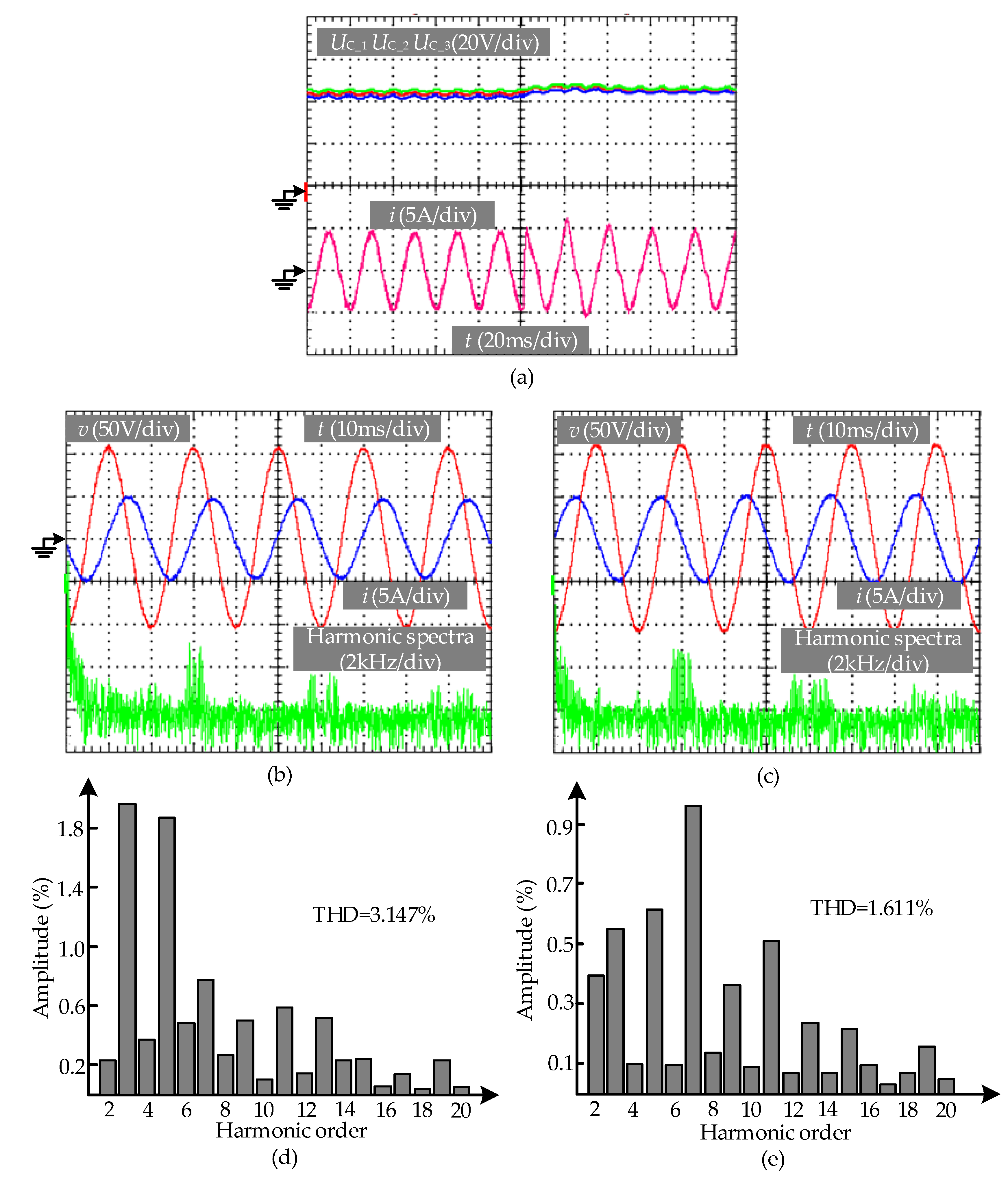
Although the proposed CPSR-PWM scheme can ensure the natural active power balance for the modules of CHB-STATCOMs, theoretically, the inherent parameter differences that exist in the modules might threaten the system’s capability to operate for a long time. Therefore, in the following experiment, a module-level capacitor voltage balance control proposed in [23] is adopted with the proposed CPSR-PWM. Figure 16 describes the experimental waveforms for this scenario.
The THDs of the compensating currents in the inductive and capacitive modes were 3.147% and 1.611%, respectively, and each single order harmonic amplitude was lower than 2% and 1%, as shown in Figure 16d,e. These indicators meet the requirements provided by IEEE Std. 519-2014 [33].
The balanced capacitor voltages and compensating current are displayed in Figure 16a. At t = 100 ms, the inductive reactive current command was changed to be the capacitive one. Figure 16b,c shows the current and voltage waveforms simultaneously, which demonstrates the phase relationship between them. Moreover, the harmonic clusters of the compensating current verify that, the equivalent switching frequency raises to 6k Hz, which is 2N (N = 3) times that of the carrier frequency 1 kHz.
6. Conclusions
This paper proposed a CPSR-PWM scheme for CHB-STATCOMs, which could eliminate the carrier phase difference influence on the active power balance for the H-bridge modules. The conclusions of the study are as follows.
(1) The carrier phase difference in the conventional unipolar double-frequency CPS-PWM for CHB-STATCOMs would result in unbalanced active power for the modules, which would cause diverged capacitor voltages and deteriorate the power quality of the compensating current.
(2) A carrier rotation scheme is proposed with the CPS-PWM method to achieve the dynamic active power balance for the modules in CHB-STATCOMs. The capacitor voltage could maintain balance without the individual capacitor voltage control or the auxiliary circuits in theory. The carrier rotation period should be an integer multiple of the reference and the rotation time should be at the reference zero-crossing point to enhance the robustness of the system.
(3) Experimental verifications are carried out on a downscaled CHB-STATCOM prototype. The results reveal the feasibility of the proposed method.
Author Contributions
Conceptualization, C.X and K.D.; methodology, C.X.; software, J.C.; validation, C.X., and J.C.; writing—original draft preparation, C.X.; writing—review and editing, J.C. and K.D.; supervision, K.D.; funding acquisition, C.X. All authors have read and agreed to the published version of the manuscript.
Funding
This research was funded by the National Natural Science Foundation of China [Research on loss optimization and capacitance reduction of capacitor-switching semi-full bridge (CS-SFB) MMC sub-module, based on SiC-MOSFETs and Si-IGBTs], grant number [51807073].
Conflicts of Interest
The authors declare no conflict of interest.
References
- Chen, C.I.; Chen, Y.C.; Chin, Y.C.; Chen, C.H. Integrated power-quality monitoring mechanism for microgrid. IEEE Trans. Smart Grid 2018, 9, 6877–6885. [Google Scholar] [CrossRef]
- Hossain, M.A.; Pota, H.R.; Issa, W.; Hossain, M.J. Overview of AC microgrid controls with inverter-interfaced generations. Energies 2017, 10, 1300. [Google Scholar] [CrossRef]
- Joksimovic, G. Transformer reactive power compensation–fixed capacitor bank calculation. IEEE Trans. Power Deliv. 2015, 30, 1629–6130. [Google Scholar] [CrossRef]
- Gyugyi, L.; Otto, R.A.; Putman, T.H. Principles and applications of static, thyristor-controlled, shunt compensator. IEEE Trans. Power Appar. Syst. 1978, 5, 1935–1945. [Google Scholar]
- Gyugyi, L. Application characteristics of converter-based FACTS controllers. In Proceedings of the International Conference on Power System Technology, Perth, WA, Australia, 4–7 December 2000; pp. 391–396. [Google Scholar]
- Wang, Y.H.; Li, Y.; Cao, Y.J.; Tan, Y.; He, L.; Han, J.Y. Hybrid AC/DC microgrid architecture with comprehensive control strategy for energy management of smart building. Int. J. Electr. Power Energy Syst. 2018, 101, 151–161. [Google Scholar] [CrossRef]
- Xu, C.; Dai, K.; Chen, X.W.; Kang, Y. Voltage droop control at point of common coupling with arm current and capacitor voltage analysis for distribution static synchronous compensator based on modular multilevel converter. IET Power Electron. 2016, 9, 1643–1653. [Google Scholar] [CrossRef]
- Kotsampopoulos, P.; Georgilakis, P.; Lagos, D.T.; Kleftakis, V.; Hatziargyriou, N. FACTS providing grid services: Applications and testing. Energies 2019, 12, 2554. [Google Scholar] [CrossRef] [Green Version]
- Han, B.M.; Baek, S.T.; Ko, J.S. New configuration of 36-pulse voltage source converter for STATCOM. In Proceedings of the 31st Annual Conference of the IEEE-Industrial-Electronics-Society, Raleigh, NC, USA, 6–10 November 2005; pp. 865–870. [Google Scholar]
- Nabae, A.; Takahashi, I.; Akagi, H. A new neutral-point clamped PWM inverter. IEEE Trans. Ind. Appl. 1981, 17, 518–523. [Google Scholar] [CrossRef]
- Choi, N.S.; Cho, J.G.; Cho, G.H. A general circuit topology of multilevel inverter. In Proceedings of the 22nd Annual IEEE Power Electronics Specialists Conference, Cambridge, MA, USA, 24–27 June 1991; pp. 96–103. [Google Scholar]
- Meynard, T.A.; Foch, H. Multi-level conversion: High voltage choppers and voltage-source inverters. In Proceedings of the 23rd Annual IEEE Power Electronics Specialists Conference, Toledo, Spain, 29 June–3 July 1992; pp. 397–403. [Google Scholar]
- Meynard, T.A.; Foch, H.; Thomas, P.; Courault, J.; Jakob, R.; Nahrstaedt, M. Multicell converters: Basic concepts and industry applications. IEEE Trans. Ind. Electron. 2002, 49, 955–964. [Google Scholar] [CrossRef]
- Peng, F.Z.; Lai, J.S.; McKeever, J.W.; VanCoevering, J. A multilevel voltage-source inverter with separate DC sources for static var generation. IEEE Trans. Ind. Appl. 1996, 32, 1130–1138. [Google Scholar] [CrossRef] [Green Version]
- Peng, F.Z.; Wang, J. A universal STATCOM with delta-connected cascade multilevel inverter. In Proceedings of the 35th Annual IEEE Power Electronics Specialists Conference, Aachen, Germany, 20–25 June 2004; pp. 3529–3533. [Google Scholar]
- Pandey, R.; Tripathi, R.N.; Hanamoto, T. Comprehensive analysis of LCL filter interfaced cascaded H-bridge multilevel inverter-based DSTATCOM. Energies 2017, 10, 346. [Google Scholar] [CrossRef] [Green Version]
- Xu, C.; Lin, L.; Yin, T.X.; Hu, J.B. An improved phase-shifted-carrier technique for hybrid modular multilevel converter with boosted modulation index. IEEE Trans. Power Electron. 2020, 35, 1340–1352. [Google Scholar] [CrossRef]
- Paris, J.M.D.; Osório, C.R.D.; Pinheiro, H.; Carnielutti, F.D.M. Phase disposition modulation with sorting algorithm for symmetrical cascaded multilevel converters. IEEE Trans. Ind. Appl. 2019, 55, 7527–7536. [Google Scholar] [CrossRef]
- Ilves, K.; Harnefors, L.; Norrga, S.; Nee, H.P. Analysis and operation of modular multilevel converters with phase-shifted carrier PWM. IEEE Trans. Power Electron. 2015, 30, 268–283. [Google Scholar] [CrossRef]
- Zha, X.M.; Yang, Z.Z.; Gong, J.W.; Li, S.S.; Liu, F.; Huang, M. Asymmetrical carrier phase-shifted pulse-width modulation for partly regenerative converter. IET Power Electron. 2017, 10, 442–450. [Google Scholar] [CrossRef]
- Solomon, L.A.; Permuy, A.; Benavides, N.D.; Opila, D.F.; Lee, C.J.; Reed, G.F. A transformerless PCB-based medium-voltage multilevel power converter with a DC capacitor balancing circuit. IEEE Trans. Power Electron. 2016, 31, 3052–3067. [Google Scholar] [CrossRef]
- Luo, L.; Zhang, Y.; Jia, L.; Yang, N.; Yang, L.; Zhang, H. Capacitor static voltage balance based on auxiliary-power supply pulse width control for MMC. IET Power Electron. 2018, 11, 1796–1803. [Google Scholar] [CrossRef]
- Liu, Z.; Liu, B.; Duan, S.; Kang, Y. A novel DC capacitor voltage balance control method for cascade multilevel STATCOM. IEEE Trans. Power Electron. 2012, 27, 14–27. [Google Scholar] [CrossRef]
- He, Y.; Duan, W.; Fu, Y. Research on DC voltage balancing control method of star connection cascaded H-bridge static var generator. IET Power Electron. 2016, 9, 1505–1512. [Google Scholar] [CrossRef]
- Yang, D.; Yin, L.; Xu, S.; Wu, S. Power and voltage control for single-phase cascaded H-bridge multilevel converters under unbalanced loads. Energies 2018, 11, 2435. [Google Scholar] [CrossRef] [Green Version]
- Xie, C.; Zhao, X.; Li, K.; Zou, J.; Guerrero, J.M. Multirate resonant controllers for grid-connected inverters with harmonic compensation function. IEEE Trans. Ind. Electron. 2019, 66, 8981–8991. [Google Scholar] [CrossRef]
- Bahrani, B.; Karimi, A.; Rey, B.; Rufer, A. Decoupled dq-current control of grid-tied voltage source converters using nonparametric models. IEEE Trans. Ind. Electron. 2013, 60, 1356–1366. [Google Scholar] [CrossRef]
- Wang, X.; Ruan, X.; Liu, S.; Tse, C.K. Full feedforward of grid voltage for grid-connected inverter with LCL filter to suppress current distortion due to grid voltage harmonics. IEEE Trans. Power Electron. 2010, 25, 3119–3127. [Google Scholar] [CrossRef]
- Adam, G. Current control of voltage source inverter with unipolar double frequency PWM. In Proceedings of the 2017 Progress in Applied Electrical Engineering (PAEE), Koscielisko, Poland, 25–30 June 2017. [Google Scholar]
- Holmes, G.; Lipo, T.A. Pulse Width Modulation for Power Converters: Principle and Practice; IEEE Press: Piscataway, NJ, USA, 2003. [Google Scholar]
- Waston, G.N. The Theory of Bessel Functions; Cambridge University Press: Cambridge, UK, 1958. [Google Scholar]
- Zhang, Y.; Dai, K.; Xu, C.; Kang, Y.; Dai, Z. Multiple sampling PSC-PWM with hierarchical control architecture for MMC-DSTATCOM. IET Electr. Power Appl. 2019, 13, 1431–1440. [Google Scholar] [CrossRef]
- IEEE Recommended Practice and Requirements for Harmonic Control in Electric Power Systems; IEEE Standard: Piscataway, NJ, USA, 2014; pp. 1–29.
Figure 1.
Configuration of star-connection the three-phase cascaded H-bridge static synchronous compensators (CHB-STATCOM) and schematic dual-loop control block diagram.
Figure 1.
Configuration of star-connection the three-phase cascaded H-bridge static synchronous compensators (CHB-STATCOM) and schematic dual-loop control block diagram.

Figure 2.
Unipolar double-frequency pulse-width-modulation (PWM).
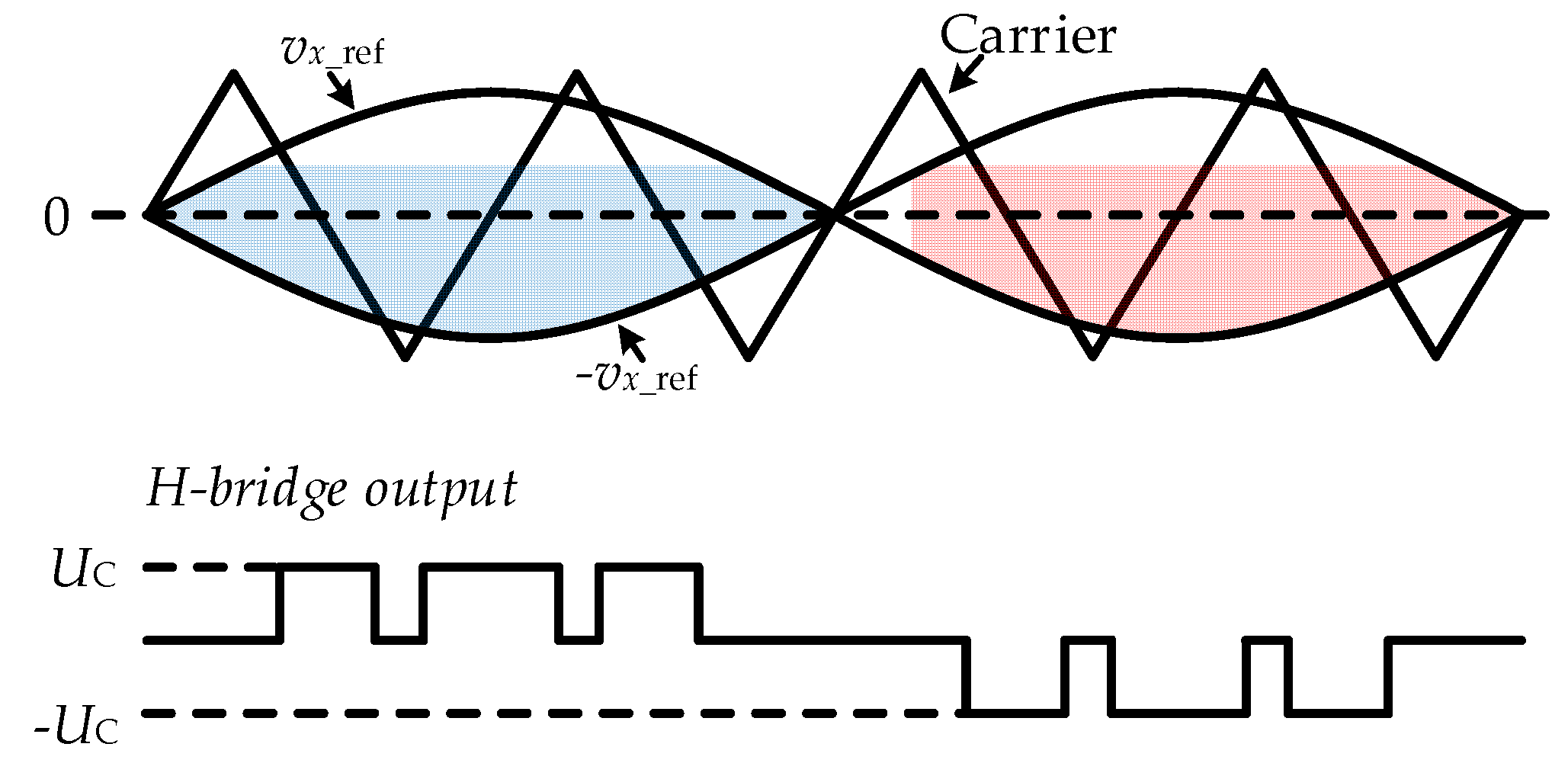
Figure 3.
Sideband harmonic vectors when N = 3. (a) m ≠ 6k, and (b) m = 6k.
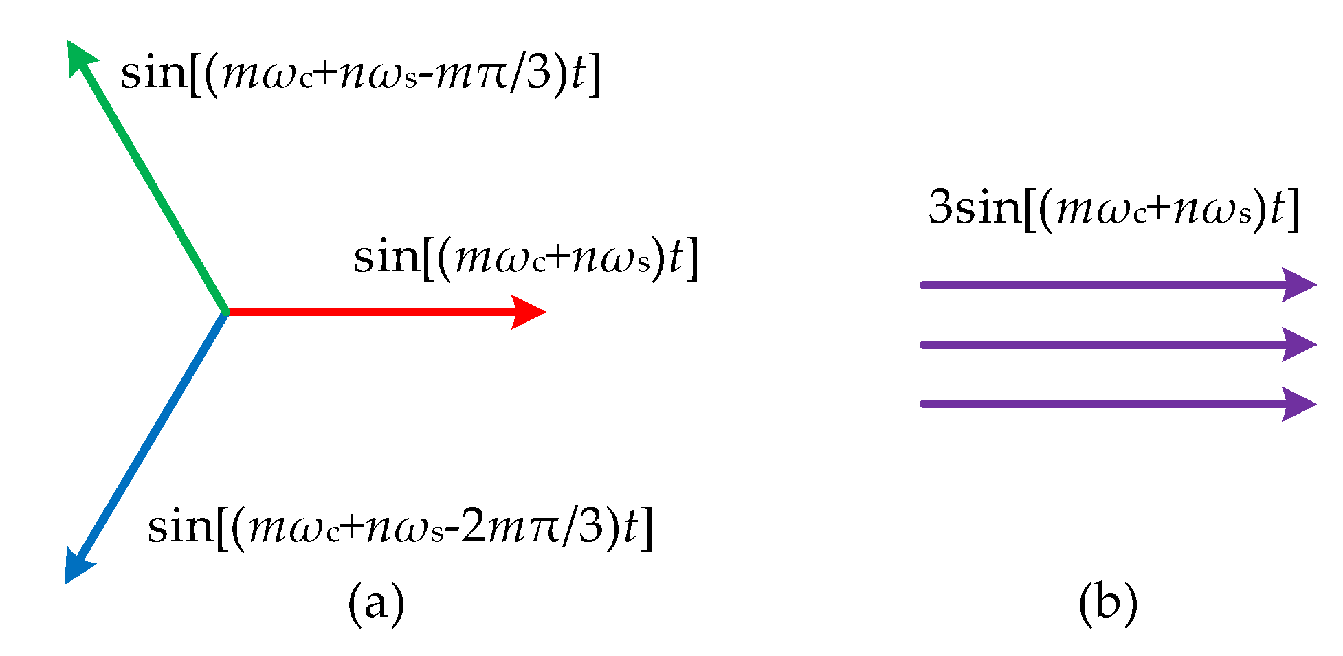
Figure 4.
Vector graphs for CHB-STATCOM in an ideal situation.
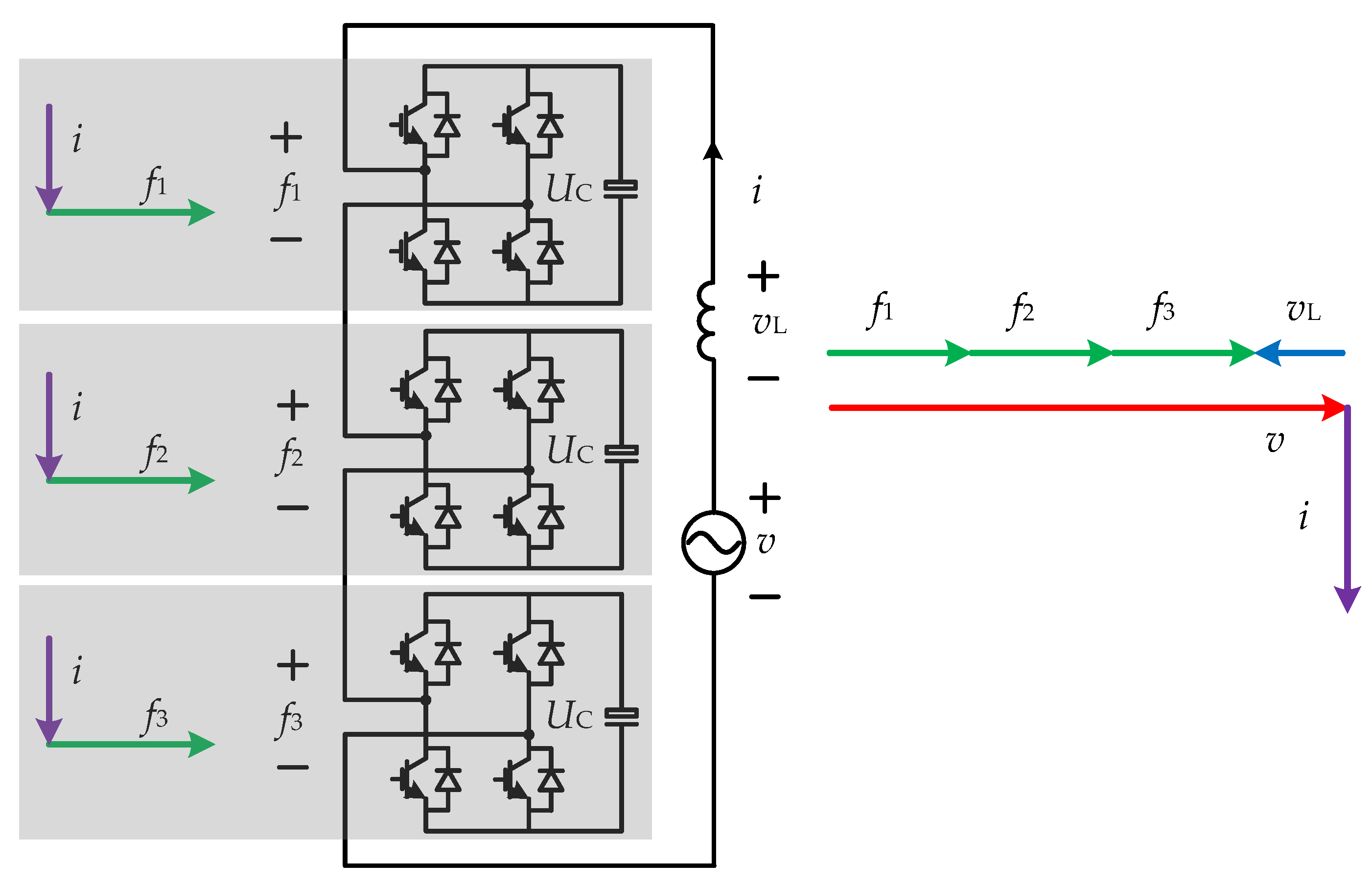
Figure 5.
Bessel function curves with different orders.
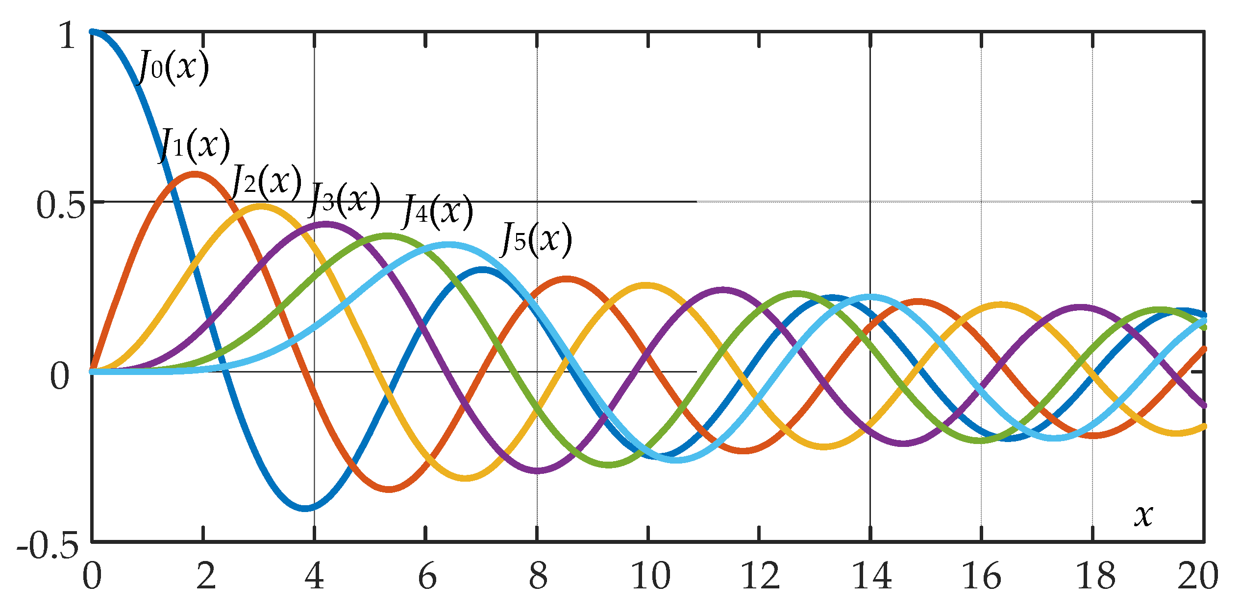
Figure 6.
Amplitude of the additional fundamental component with varied modulation index M and carrier ratio K.
Figure 6.
Amplitude of the additional fundamental component with varied modulation index M and carrier ratio K.
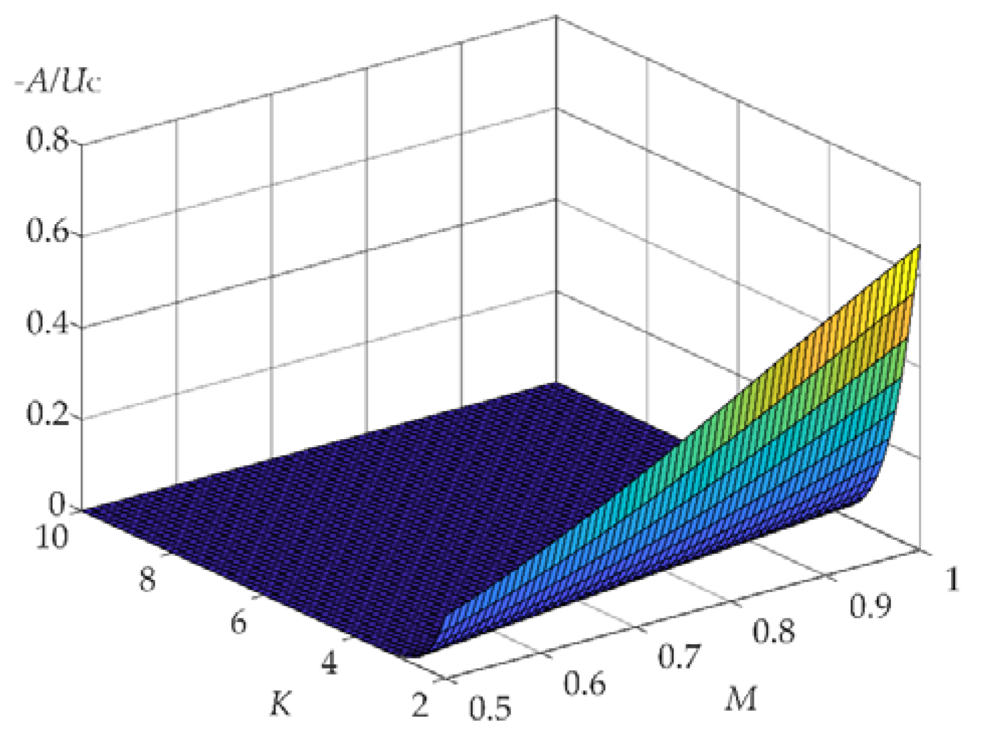
Figure 7.
Vector graphs for modules considering additional fundamental components in output voltage.
Figure 7.
Vector graphs for modules considering additional fundamental components in output voltage.
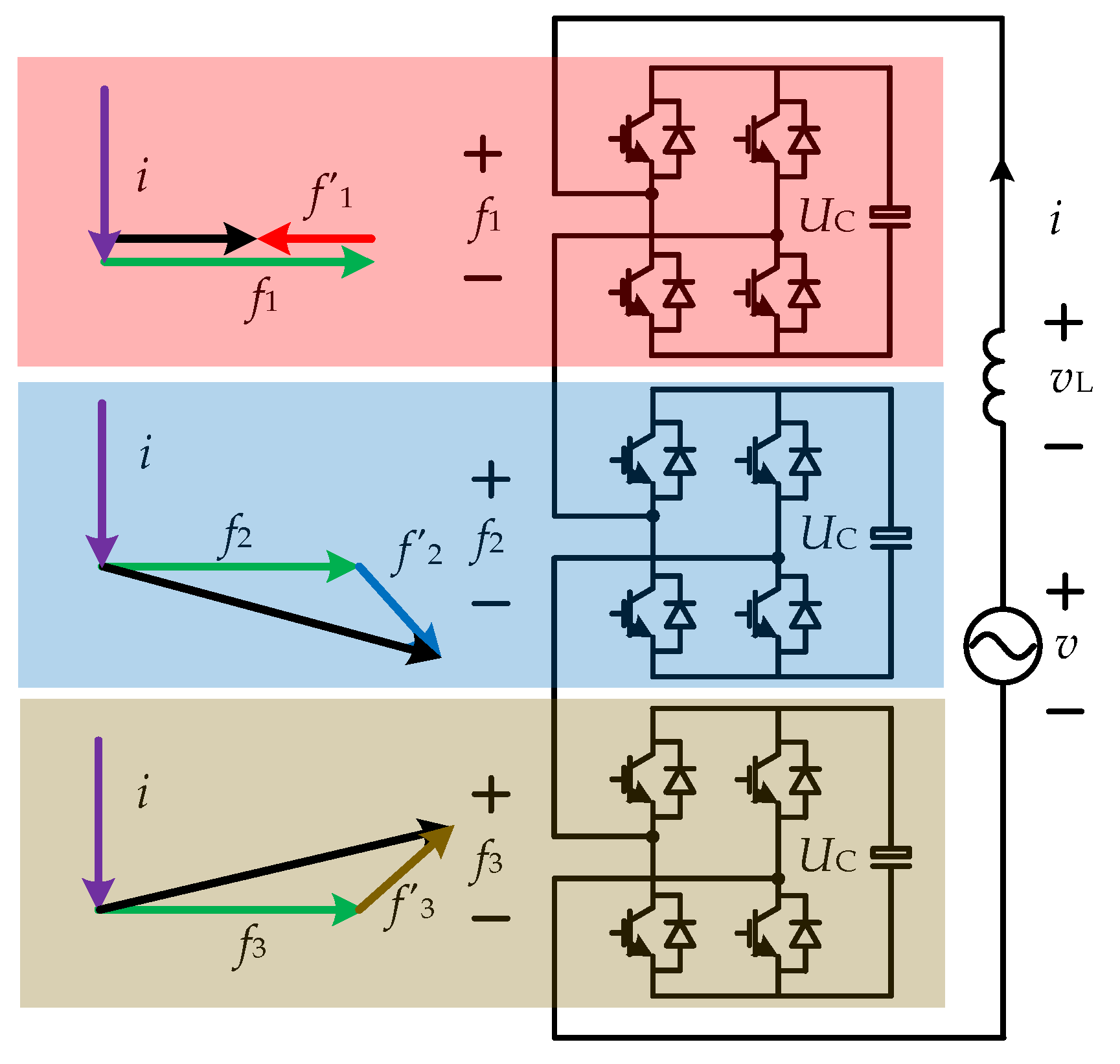
Figure 8.
CPRS-PWM scheme with rotation time at reference zero-crossing point.

Figure 9.
CPRS-PWM scheme with the rotation time at the reference maximum point.

Figure 10.
CPRS-PWM scheme with asynchronous rotation time at reference zero-crossing point.
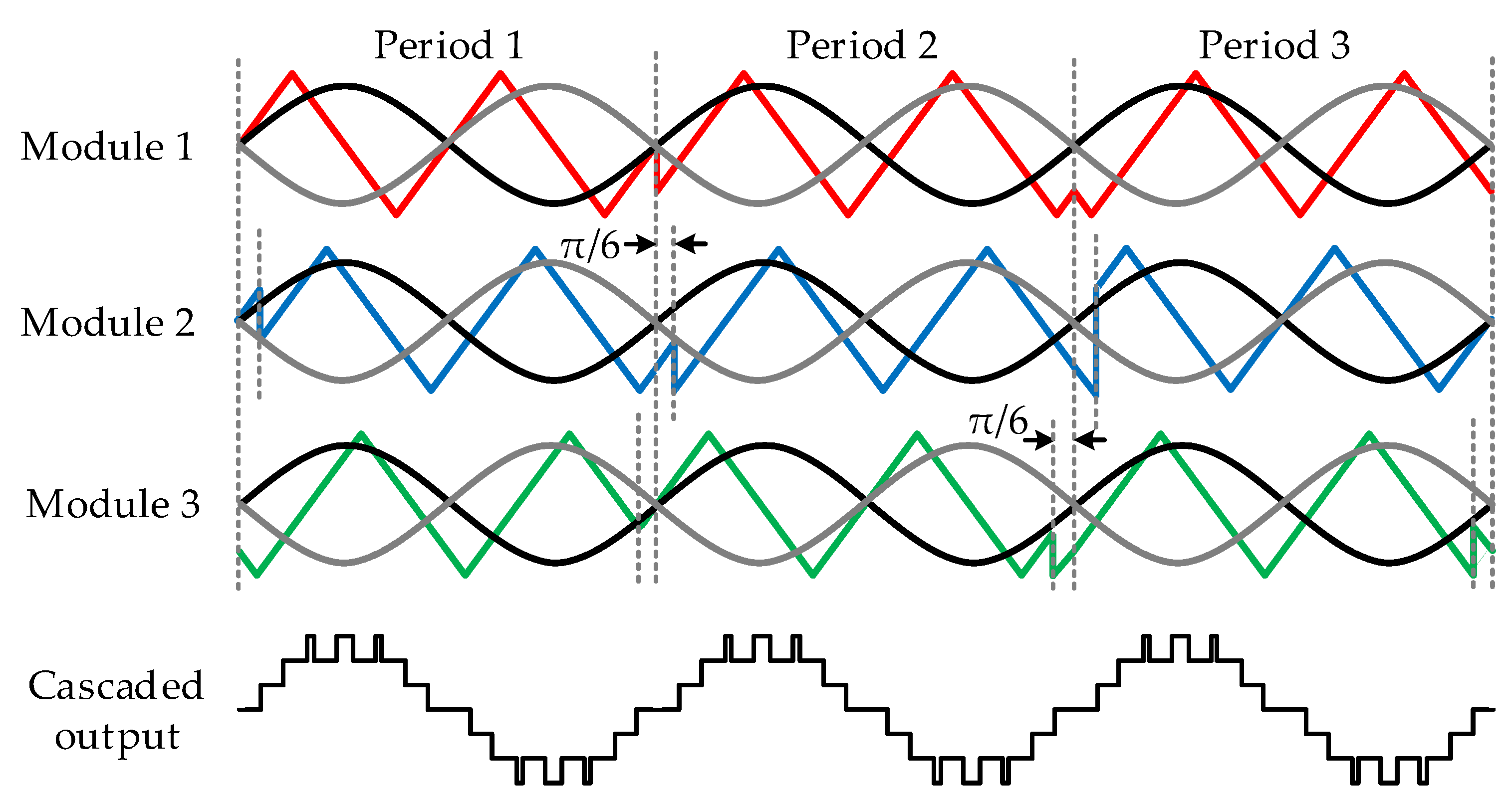
Figure 11.
CPRS-PWM scheme with asynchronous rotation time at maximum point of reference.
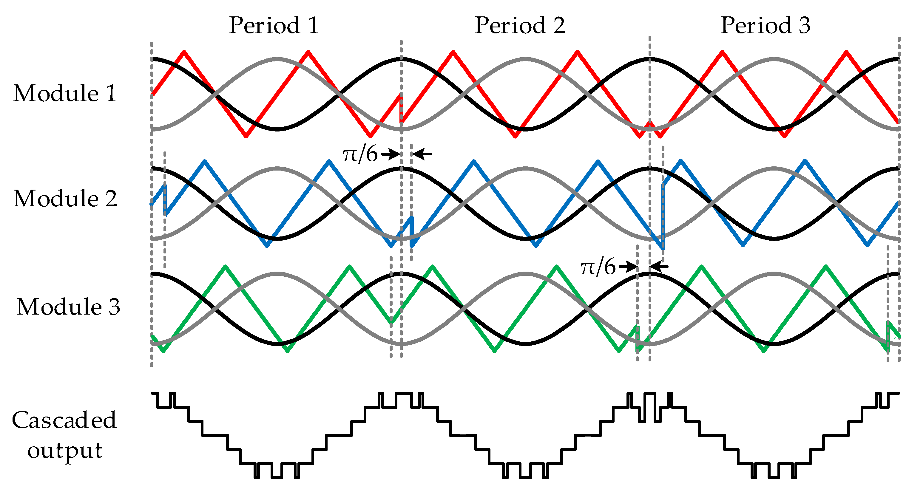
Figure 12.
THDs of the cascaded output voltage with different asynchronous rotation time and carrier ratio K = 2.
Figure 12.
THDs of the cascaded output voltage with different asynchronous rotation time and carrier ratio K = 2.
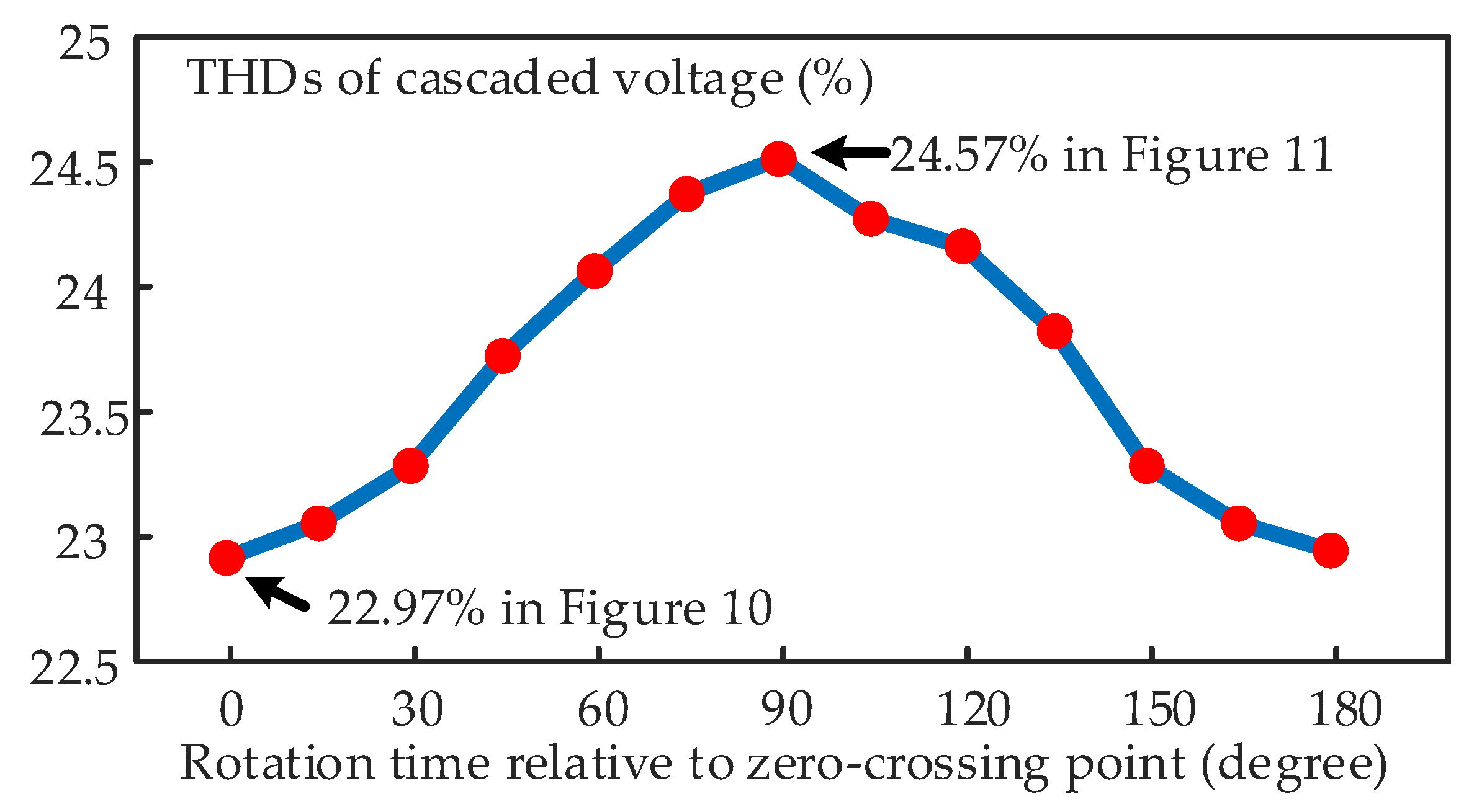
Figure 13.
The THDs of the cascaded output voltage with different asynchronous rotation time and carrier ratio K = 4.
Figure 13.
The THDs of the cascaded output voltage with different asynchronous rotation time and carrier ratio K = 4.
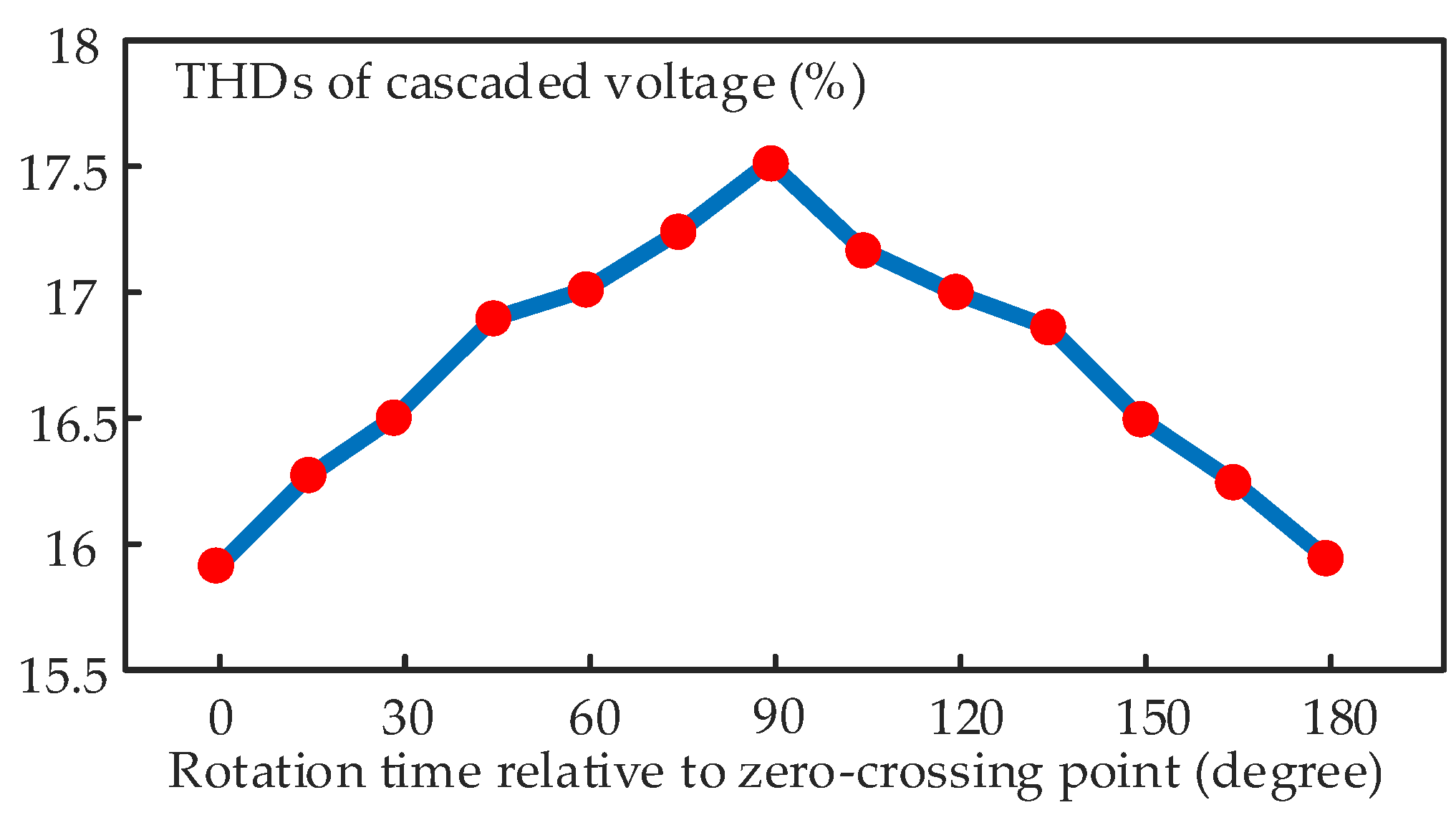
Figure 14.
Module picture of CHB-STATCOM prototype and hierarchical control structure.

Figure 15.
Experimental waveforms of the capacitor voltages, the grid voltage, and the compensating current, verifying the feasibility of the proposed CPSR-PWM, (a1) and (a2). Capacitor voltages with the conventional CPS- and the proposed CPSR-PWM schemes, (b1) and (b2). Grid voltage and compensating current with the conventional CPS- and the proposed CPSR-PWM schemes, (c1) and (c2). Fourier analysis of the compensating current with the conventional CPS- and the proposed CPSR-PWM schemes.
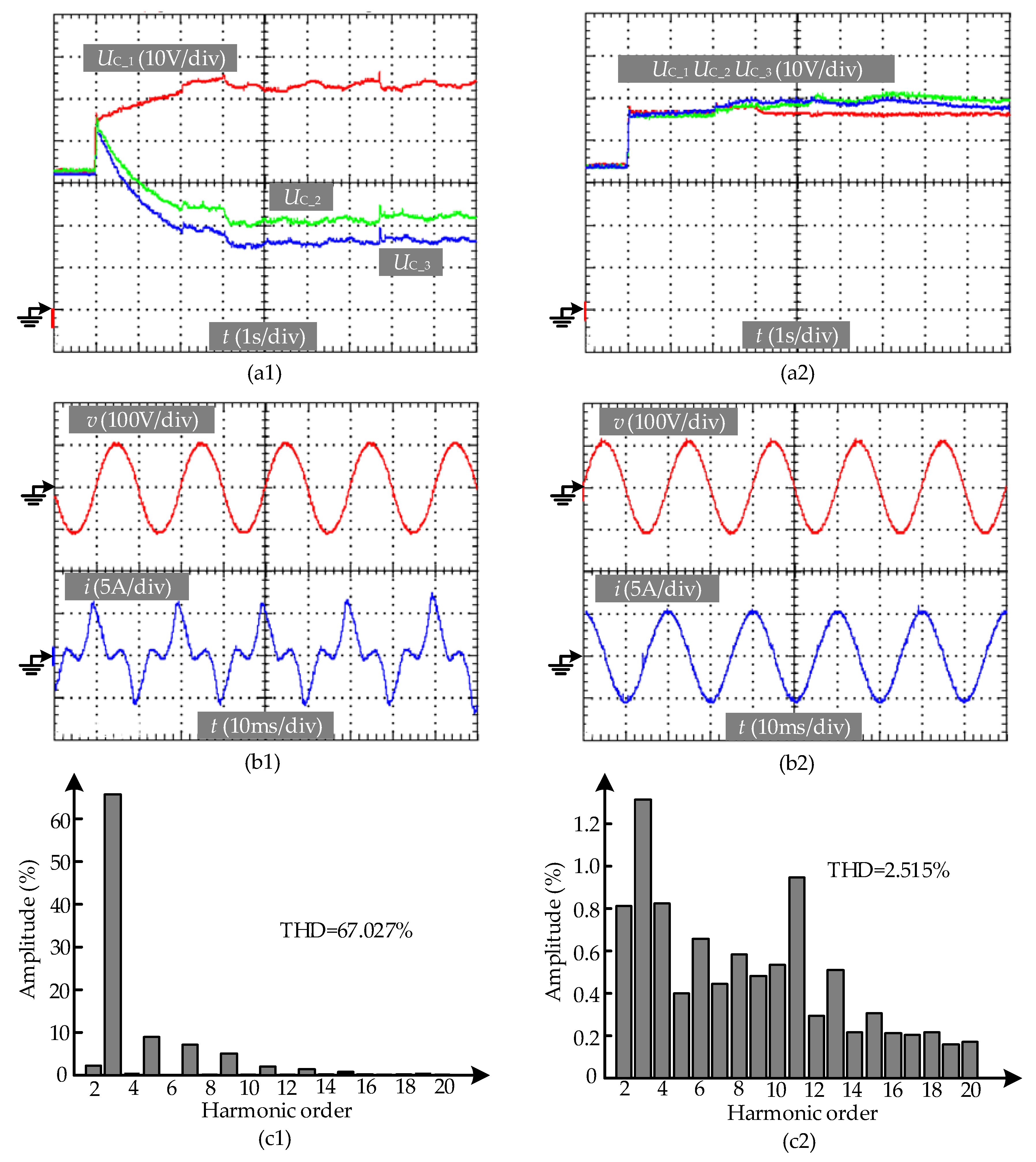
Figure 16.
Steady-state experimental waveforms of capacitor voltages, grid voltage, and compensating current. (a). Capacitor voltages and compensating currents from inductive to capacitive mode. (b) Grid voltage, compensating current, and its harmonic distribution in the inductive mode. (c) Grid voltage, compensating current, and its harmonic distribution in the capacitive mode. (d) Fourier analysis of compensating current in the inductive mode. (e) Fourier analysis of the compensating current in the capacitive mode.

Table 1.
Total harmonics distortion (THD) analysis of the cascaded output voltages, shown in Figure 10 and Figure 11.
| Period 1 | Period 2 | Period 3 | Period 1~3 | |
|---|---|---|---|---|
| Zero-crossing | 24.81% | 24.63% | 24.62% | 22.97% |
| Maximum point | 24.97% | 29.43% | 29.42% | 24.57% |
Table 2.
System parameters in the experiment.
| Parameters | Symbols | Values |
|---|---|---|
| Cascaded module number | N | 3 |
| Root-mean-square value of grid voltage | v | 82 V |
| Module capacitance | C | 4.7 μF |
| Compensating current reference | Iq_ref | 5 A |
| Rated capacitor voltage | UC_ref | 48 V |
| Buffer inductance | L | 8 mH |
| Fundamental/reference frequency | f | 50 Hz |
| Carrier frequency | fc | 1k Hz |
| Equivalent switching frequency | fE | 6k Hz |
| Sampling frequency | fs | 6k Hz |
© 2020 by the authors. Licensee MDPI, Basel, Switzerland. This article is an open access article distributed under the terms and conditions of the Creative Commons Attribution (CC BY) license (http://creativecommons.org/licenses/by/4.0/).
Share and Cite
MDPI and ACS Style
Xu, C.; Chen, J.; Dai, K. Carrier-Phase-Shifted Rotation Pulse-Width-Modulation Scheme for Dynamic Active Power Balance of Modules in Cascaded H-Bridge STATCOMs. Energies 2020, 13, 1052. https://doi.org/10.3390/en13051052
AMA Style
Xu C, Chen J, Dai K. Carrier-Phase-Shifted Rotation Pulse-Width-Modulation Scheme for Dynamic Active Power Balance of Modules in Cascaded H-Bridge STATCOMs. Energies. 2020; 13(5):1052. https://doi.org/10.3390/en13051052
Chicago/Turabian StyleXu, Chen, Jingjing Chen, and Ke Dai. 2020. "Carrier-Phase-Shifted Rotation Pulse-Width-Modulation Scheme for Dynamic Active Power Balance of Modules in Cascaded H-Bridge STATCOMs" Energies 13, no. 5: 1052. https://doi.org/10.3390/en13051052
Note that from the first issue of 2016, this journal uses article numbers instead of page numbers. See further details here.