Current Balancing Algorithm for Three-Phase Multilevel Current Source Inverters


Electrical Engineering Department, Colorado School of Mines, Golden, CO 80401, USA
*
Authors to whom correspondence should be addressed.
Energies 2020, 13(4), 860; https://doi.org/10.3390/en13040860
Submission received: 9 January 2020
/
Revised: 8 February 2020
/
Accepted: 12 February 2020
/
Published: 16 February 2020
(This article belongs to the Special Issue Applied Neural Networks and Fuzzy Logic in Power Electronics, Motor Drives, Renewable Energy Systems and Smart Grids)
Abstract
:In high power, medium voltage applications, Current Source Inverters CSIs are connected in parallel to accommodate high DC currents. Using a proper multilevel modulation technique, parallel-connected CSIs can operate as a Multilevel CSI (MCSI). The most common modulation technique for MCSIs is the Phase-Shifted Carrier SPWM (PSC-SPWM). The proper operation of the MCSI requires each CSI modules to have the same average current flowing through its sharing inductors. In practice, the average currents of the CSI modules deviate from their nominal values. Therefore, current balancing mechanisms must be implemented. In the literature, several solutions have been proposed to tackle the current imbalance problem. Most of these solutions are based on altering the phase-shift or magnitude of the carrier waveforms of the PSC-SPWM. They require dedicated PI controllers and they are applicable to MCSIs with specific numbers of levels. This paper proposes a Current Balancing Algorithm (CBA) that can be implemented in any MCSI with any number of levels. The proposed CBA does not require any PI controllers, nor does it require any alteration to the PWM carrier waveforms. The CBA is implemented using a modified Level-Shifted SPWM (LS-PWM). The modified LS-SPWM is shown to produce lower THD and lower di/dt when compared to the PSC-SPWM. The CBA and modified LS-SPWM where implemented in a proof-of-concept lab prototype. The experimental results are presented for the five-level and seven-level cases.
1. Introduction
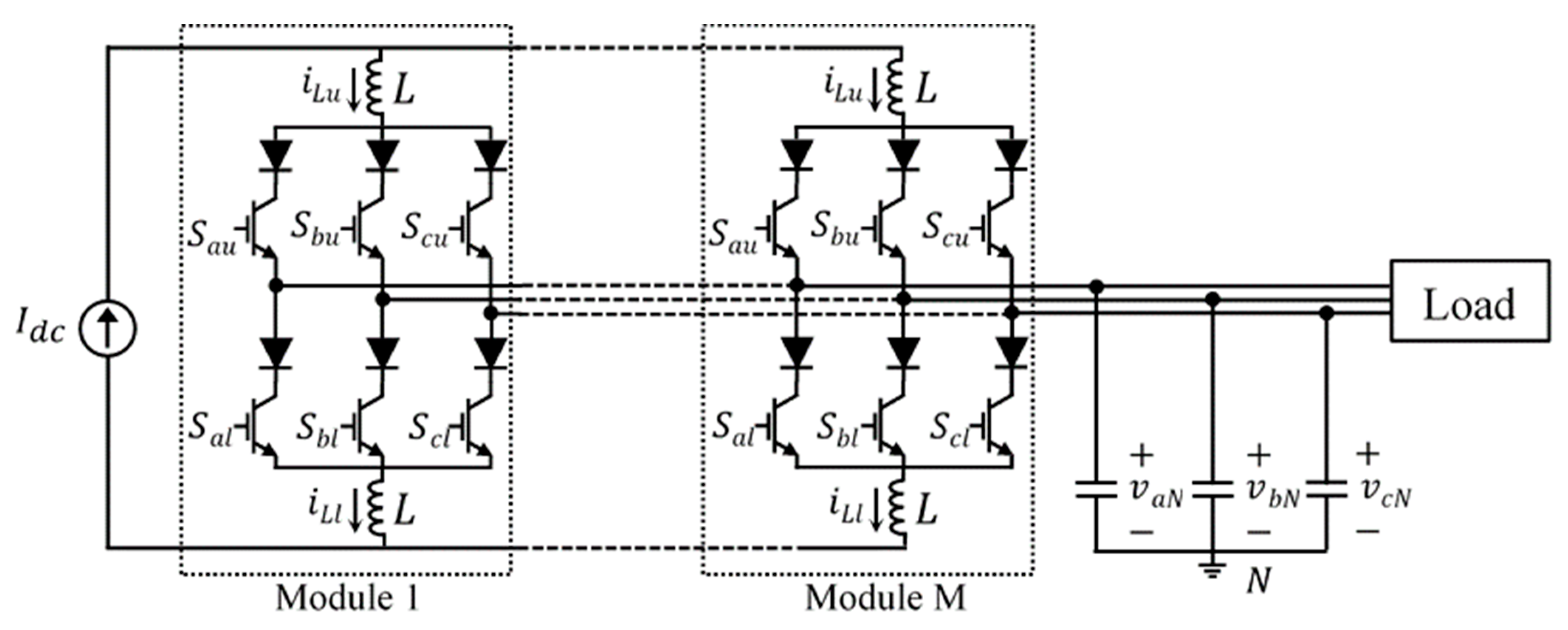
Current Source Inverters (CSIs) have been used as alternatives to Voltage Source Inverters (VSIs) in applications such as: motor drives [1], STATCOMs [2], High Voltage Direct Current (HVDC) transmission stations [3], and renewable energy conversion systems [4]. Compared to VSIs, CSIs have several advantages and drawbacks. Their advantages include inherent fault tolerance and voltage boosting capabilities. Their main drawbacks are larger ohmic losses in their DC inductors and heavy inductor cores. Nevertheless, ongoing research in the field of High Temperature Superconductors (HTS) has yielded promising results [5,6,7]. In [6], utilizing HTS coils was shown to reduce a generator’s losses and weight by half and one third, respectively. In the future, access to HTS inductors, with virtually zero ohmic and core losses will make CSIs more attractive to a broader range of applications.
In high power, medium voltage applications, several VSIs or CSIs are connected in parallel to divide the high DC current evenly between them. For these applications, CSIs are more attractive because parallel-connected CSIs can operate as a Multilevel Current Source Inverter (MCSI). MCSIs generate higher quality current waveforms that require smaller output capacitors and lower switching frequency.
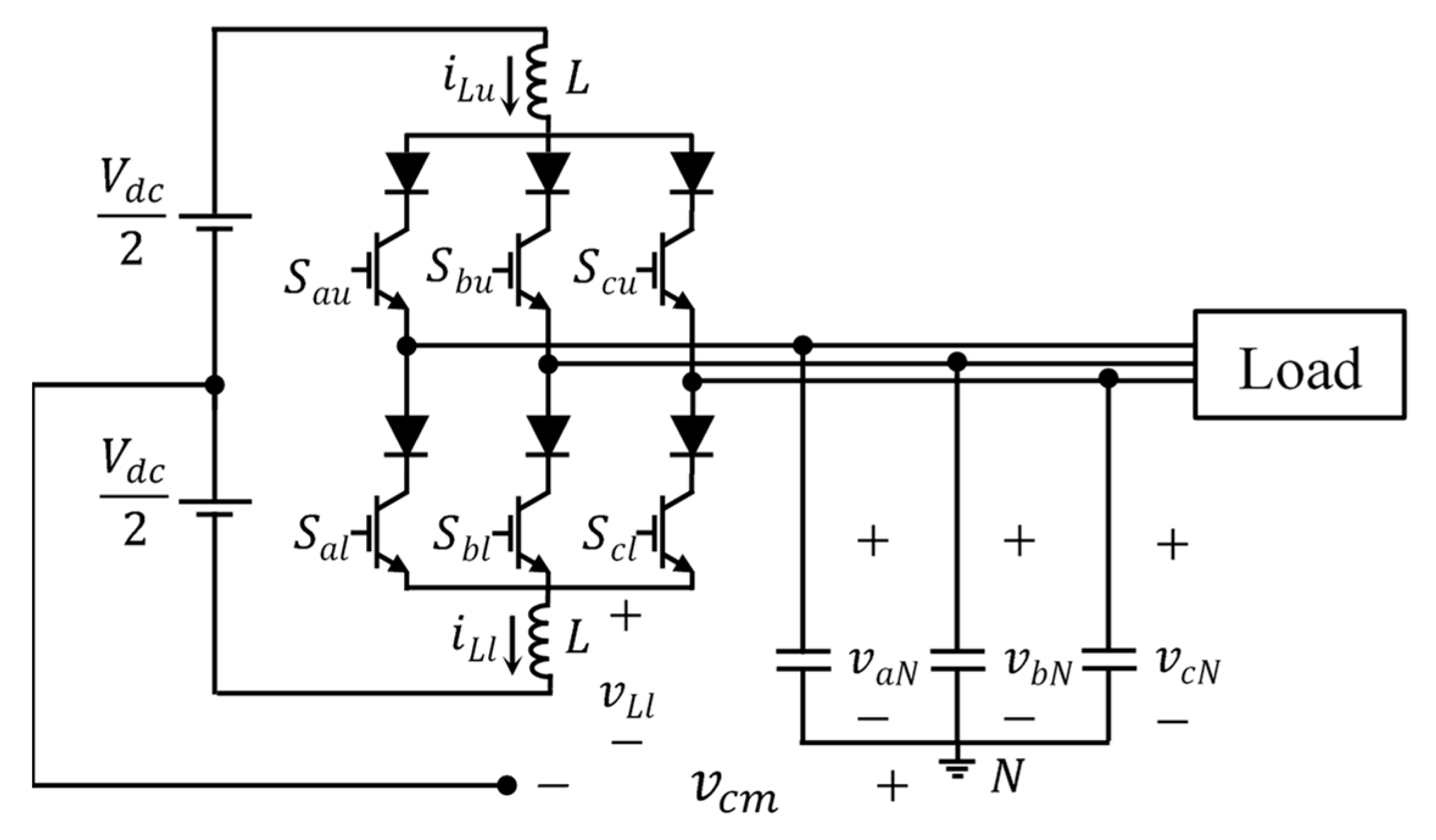
Over the past few decades, several attempts have been made to conceive an effective MCSI topology. Relying on the duality principle [8], most topologies require the DC input to be a constant current source. In most cases, either a DC voltage source connected to a large smoothing inductor [9,10] or a current-controlled buck converter [11,12,13,14] is used as a constant current source. The most common three-phase MCSI is shown in Figure 1. It was first introduced by Xiong et al. [9] and has been the subject of several papers over the past few years [10,11,12,13,14]. In addition to a current-controlled buck converter or a large smoothing inductor at the input, this topology consists of modules, for a level converter. Each module contains six controllable unidirectional switches, an upper inductor, and a lower inductor. The upper and lower inductors are referred to as sharing inductors and they are only rated for of the DC current, where the current-controlled buck converter or large smoothing inductor at the input must be rated for the full input current. A unidirectional controllable switch may be realized using a Gate Turn-Off Thyristor (GTO), an Integrated Gate-Controlled Thyristor (IGCT), a Reverse-Blocking Insulated-Gate Bipolar Transistor IGBT (RB-IGBT), or a regular IGBT connected, in series, to a diode, as shown in Figure 1.
For proper operation of the MCSI, the values of the sharing inductors in each module must be identical. The main challenge in this topology is ensuring the main DC current is divided between the modules evenly. In [9], since a six-level staircase modulation was used, an optimized fixed switching sequence was proposed. The sequence minimizes the switching losses while ensuring the volt-second area remains close to zero for each inductor under steady-state conditions. Unfortunately, this method becomes very complex and unreliable when Pulse Width Modulation (PWM) techniques are used for a higher number of levels. Moreover, the number of levels achieved was six for a three-module converter; the zero level was not achieved using the staircase modulation.
In [11], a prototype of the same topology was built and tested. The input of the inverter, in this case, was a current-controlled buck converter. The modulation technique used was the Phase-Shifted Carrier Sinusoidal PWM (PSC-SPWM) [13]. The PSC-SPWM allows individual modules to be modulated independently using the so-called “tri-logic” SPWM [15]. To synthesize multilevel waveforms using the PSC-PWM, the phase-shift between any two adjacent module’s carrier signals is set to . Although no current balancing technique was used, the average currents of the sharing inductors remained within a reasonable range of each other. Nonetheless, implementing such an inverter in a non-controlled environment, such as industrial applications, with no means to ensure a current-balanced operation is not safe. Disturbances and small differences in the electrical parameters between the modules can easily lead different inductors to have different average currents [11], and modules sustaining currents higher than their rated current could be damaged. The current imbalance problem is highlighted in [12]. Using the same modulation technique as that used in [11], the authors suggested two Proportional-Integral (PI) controllers-based solutions to ensure a current-balanced operation for the seven-level case. The first solution is to allow each module to use a small variation in the magnitude of carrier waveform as a control variable. The second solution is to allow the use of the phase-shift angle of the carrier waveform as a control variable. In both cases, to understand the input–output relationship, systems identification procedures were carried out. Both solutions were verified via simulation only, and both yielded satisfactory results. Another attempt to realize a current-balanced operation was presented in [14] where an improved version of the first solution proposed in [12] was implemented. The solution targets the seven-level case. It involved two dedicated PI controllers varying the magnitudes of the PSC-SPWM carrier waveforms. The effectiveness of the solution was verified via simulation and experimental results. However, there are several disadvantages to the proposed solutions [12,14]. By requiring multiple, dedicated, current-balancing, closed-loop control systems, the converter cost and complexity increases. Besides, the proposed alteration to the carrier waveforms has a negative impact on the Total Harmonic Distortion (THD).
This paper focuses on the voltage fed version of the MCSI. In the voltage fed MCSI, the modules are connected directly to the DC bus. Unlike the MCSI discussed in [9,10], a main smoothing inductor is not required here. This makes the MCSI modular and it reduces the number of required inductors. Also, unlike the MCSI considered in [11,12,13,14], the voltage fed MCSI does not need to be connected to the output of a current-controlled buck converter. Adding a buck converter to the input increases the cost, size, and complexity while reducing the boosting ratio of the MCSI. To compute the boosting ratio of the MCSI, the AC side power in Equation (1) is equated to the DC side power in Equation (2), assuming a lossless system. The resulting boosting ratio is given in Equation (3). In Equation (1), is the modulation index of the MCSI, is the peak value of the line-to-neutral voltage on the AC side of the MCSI, and is the power factor. In Equation (2), is the duty cycle of the current-controlled buck converter. The impact of on the boosting ratio is evident in Equation (3). If the buck converter is eliminated, the boosting ratio can be derived by assuming . Therefore, eliminating the buck converter maximizes the boosting ratio.
The main contribution of this paper is the introduction of a new Current Balancing Algorithm (CBA) to address the current imbalance issue in MCSIs. The CBA can be implemented in any MCSI regardless of the number of levels and it does not require any modification to the carrier’s waveform, unlike the balancing methods in [12,14]. Moreover, the PWM technique used in this paper is a modified version of the Level-Shifted SPWM (LS-SPWM). It was first introduced to eliminate common-mode voltage in three-level Neutral-Point-Clamped (NPC) VSIs [16]. However, its implementation in MCSI has never been discussed or demonstrated in the literature. Compared to the widely used PSC-SPWM [13], the modified LS-SPWM produces lower THD and .
The rest of the paper is divided into four main sections. Section 2 presents the modified LS-SPWM. Section 3 explains how to solve the current-imbalance problem using the CBA. Section 4 presents experimental results verifying the CBA and modified LS-SPWM using a proof-of-concept prototype. The prototype has three modules. Therefore, it can operate as either a five-level MCSI, by only utilizing two modules, or a seven-level MCSI, by utilizing all three modules. Waveforms demonstrating the operation of the five-level and seven-level cases are presented. Finally, concluding remarks are presented in Section 5.
2. Modified LS-SPWM Suitable for MCSIs
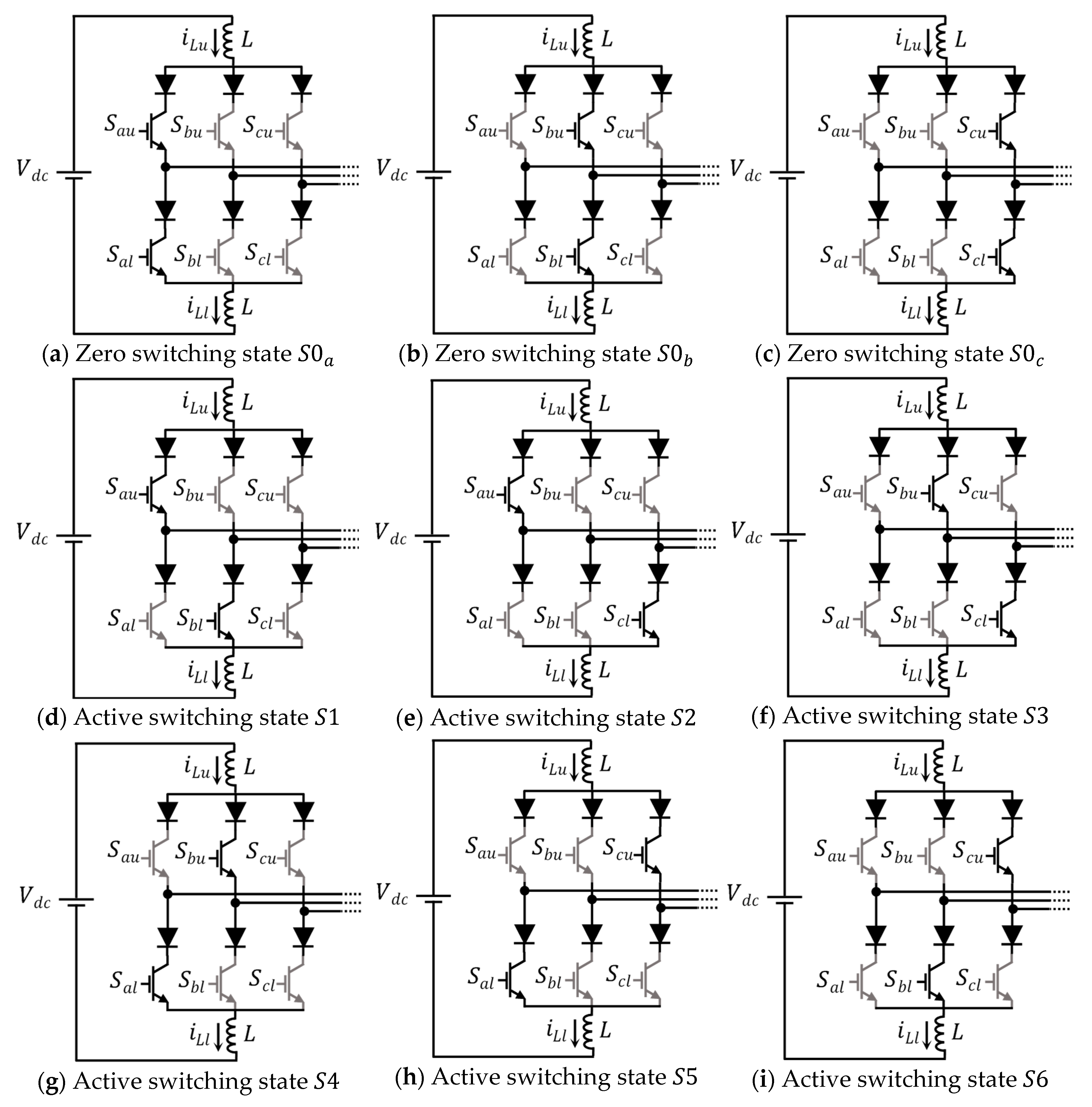
An individual CSI must have one upper switch and one lower switch switched ON at any given instance [15]; this ensures that and will always have a circulation path. Therefore, the CSI has nine possible switching states. These states can be divided into three zero states and six active states, as illustrated in Figure 2. Zero states produce zero in all phases at the AC side while active states produce a positive current in one phase and a negative current in a different phase. It is important to note that any set of three-phase currents synthesized by the CSI using any switching state shown in Figure 2 will always add up to zero. Hence, any multilevel PWM technique must produce a set of three-phase currents that always adds up to zero. It has been was shown [16] that the Level-Shifted SPWM (LS-SPWM) does not satisfy this requirement. A simple solution is described in [16] for the three-level case. The same solution can be extended to any number of levels as follows:
- (1)
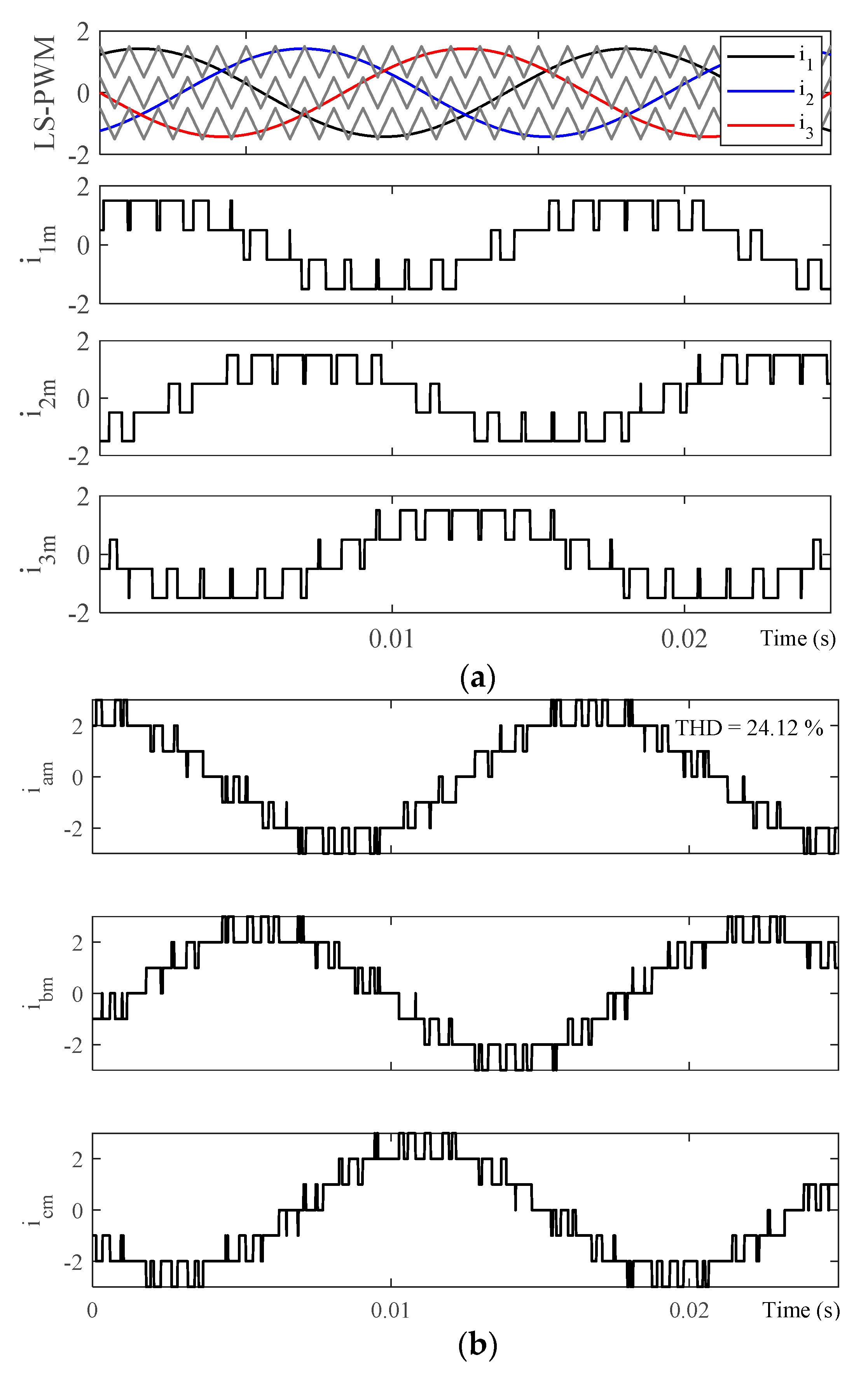
- Generate a set of three-phase modulated signals using the reference signals in Equations (4)–(6), is the modulation index and is the number of modules. The modulated signals should be generated by comparing Equations (4)–(6) to level-shifted triangle waveforms.
- (2)
- A balanced set of three-phase currents, which add up to zero, can be obtained by computing Equations (7)–(9), where , , and are the modulated signals of Equations (4)–(6).
The obtained currents in Equations (7)–(9) have levels. Their magnitude is . To extend the upper limit of to , instead of 1, a third harmonic component with a magnitude of can be added to Equations (4)–(6) [17].
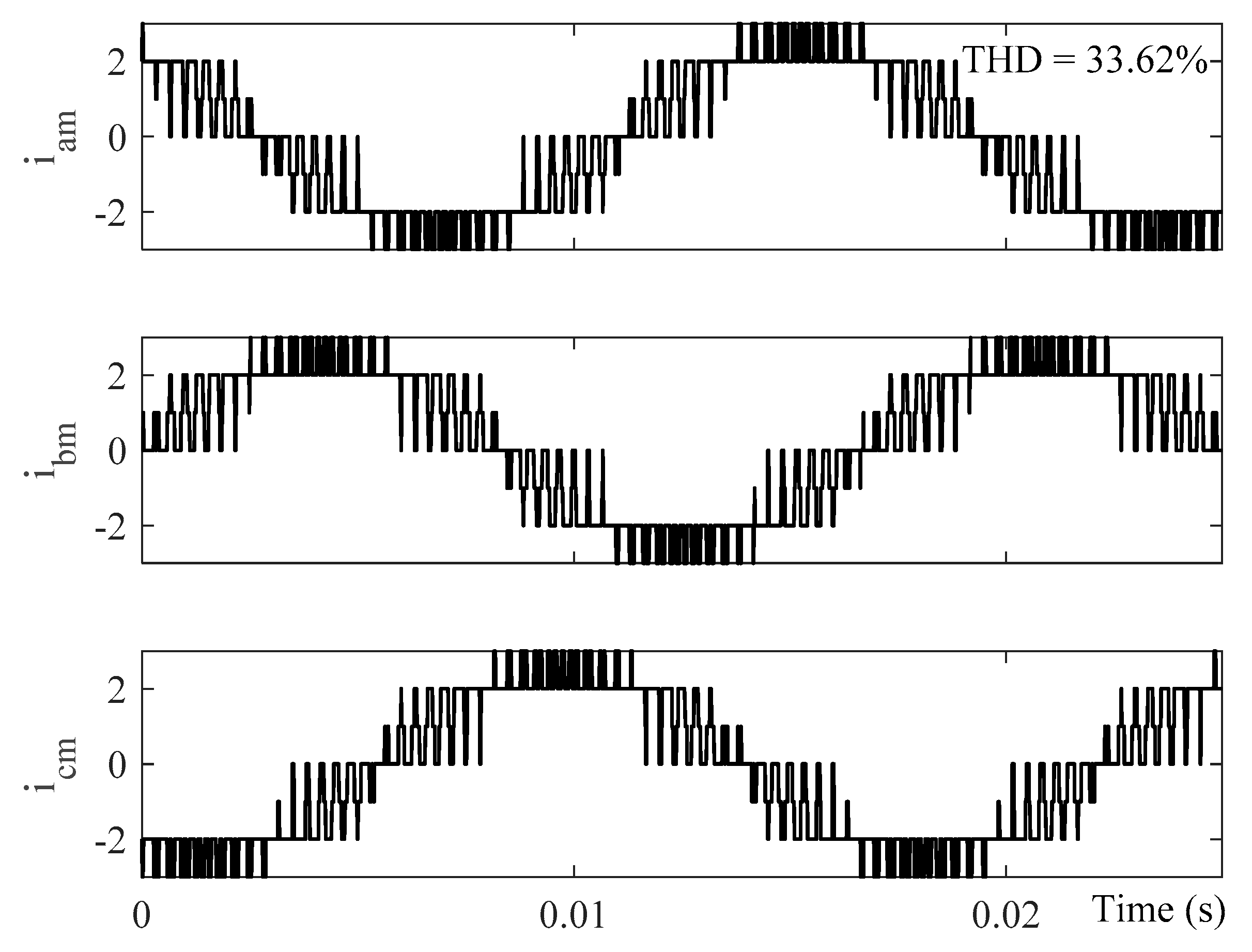
The process described above is shown in Figure 3 for a seven-level case, . The modulated signals of Equations (4)–(6) are shown in Figure 3a while Equations (7)–(9) are shown in Figure 3b. For comparison, a set of three-phase currents were produced using the PSC-SPWM [10,11,12,13,14], as shown in Figure 4. The modified LS-SPWM resulted in a lower THD, 24.12% compared to 33.62% for the PSC-SPWM. Also, unlike the PSC-SPWM, the modified LS-SPWM results in modulated waveforms where the transition from one level to the next happens consecutively, i.e., the modulated waveforms increase or decrease by one level at a time. This results in a lower , which produces less Electromagnetic Interference (EMI).
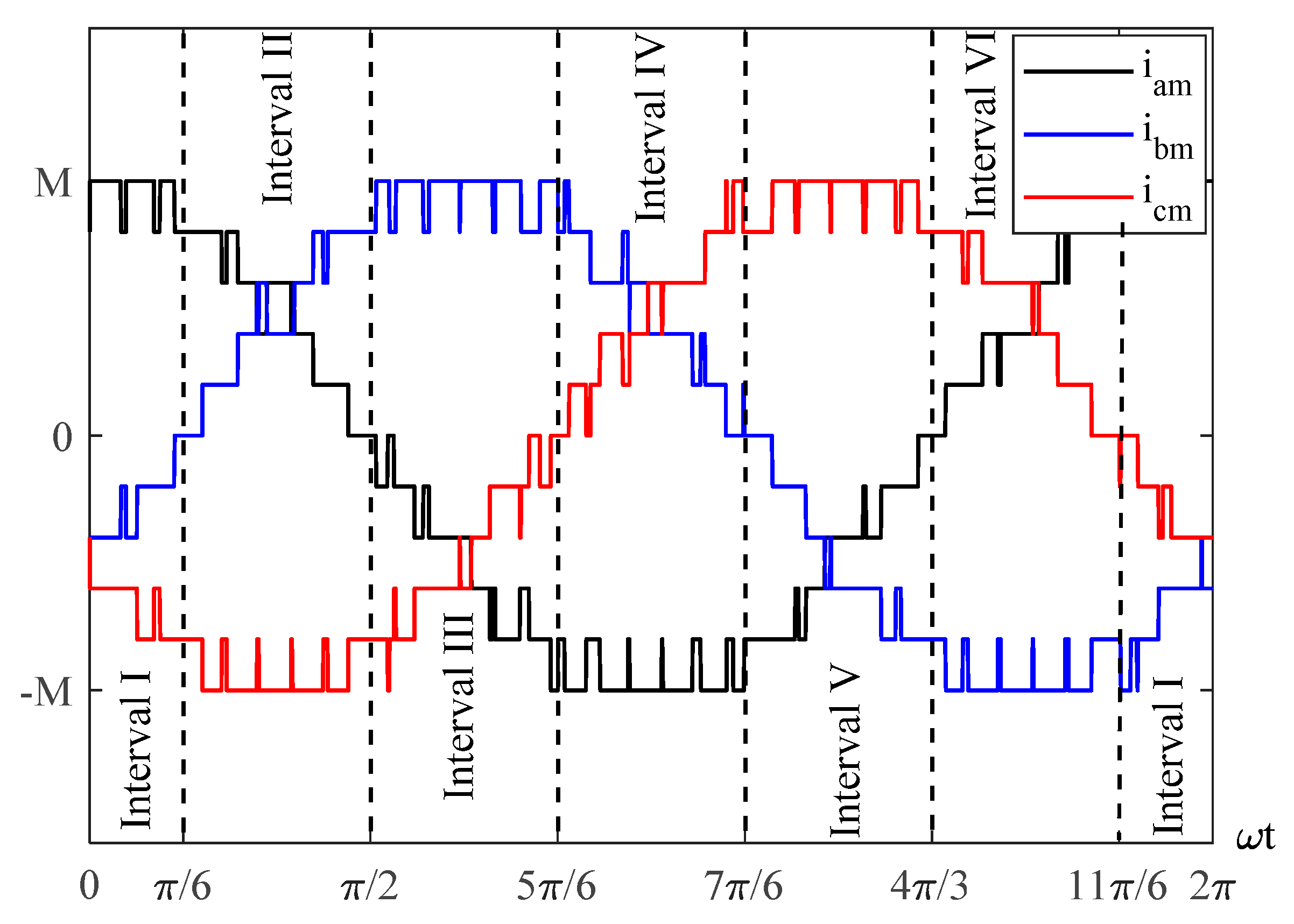
Another requirement that must be fulfilled by the modified LS-SPWM is the even and efficient distribution of the zero states among the phase legs of the modules. A CSI module has three zero switching states, see Figure 2a–c. The modified LS-SPWM should be able to determine which zero state should be selected every time a zero state is required. In a previous study [15], the zero states distribution of the CSI is determined based on the extreme values of the three-phase reference currents. The same mechanism can be used here. Based on which phase has a positive or negative peak, the fundamental cycle can be divided into six intervals, as shown in Figure 5. For example, during interval I, phase A has a positive peak. Therefore, depending on , must be switched ON in most modules. During interval IV, on the other hand, phase A has a negative peak. Hence, must be switched ON in most modules. During intervals I and IV, shortening leg A is the most efficient way to realize a zero state. Thus, during interval I, is switched ON in all modules while is switched ON in modules. Similarly, during interval IV, is switched ON in all modules while is switched ON in modules. Here, , , and are the instantaneous values of the modulated three-phase currents, their values are between and . The same procedure can be repeated for the other four intervals where phases B and C have their positive and negative peaks. Table 1 summarizes the zero states distribution mechanism over one cycle. For each interval, the corresponding number of ON upper and lower switches of each phase of the MCSI is given.
3. Current Balancing Algorithm
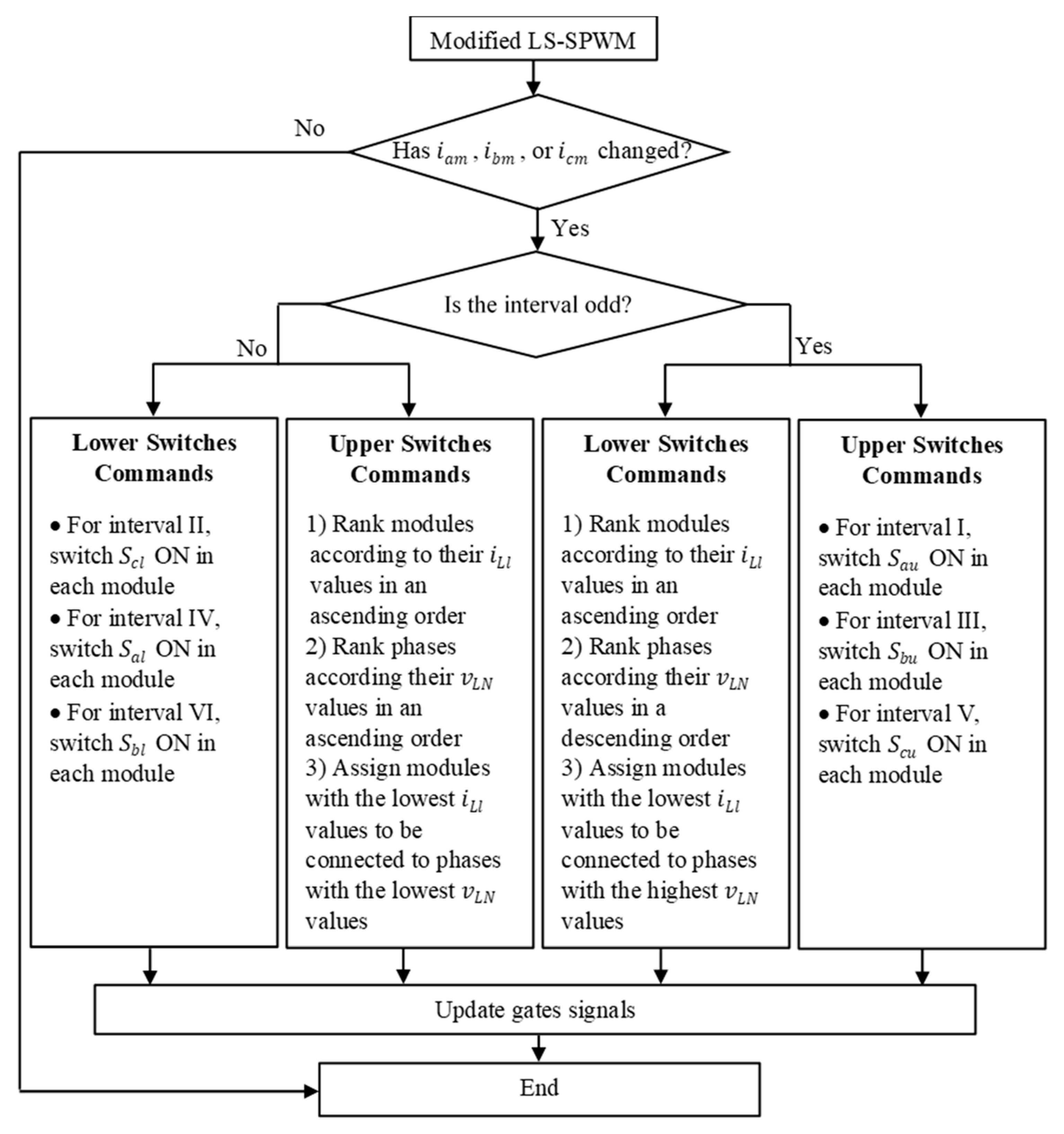
Table 1 provides the total number of ON switches for all the modules in the MCSI at any given instance. In odd intervals, the commands for the upper switches in each module are the same, the upper switch of a specified phase is turned ON in every module. On the other hand, the numbers of lower switches that should be turned ON in each phase of the MCSI are different. During Interval I, for example, Table 1 specifies how many modules should have their , , and switched ON without mapping these commands to specific modules. During even intervals, the reverse is true. In this section, an optimized selection process referred to as CBA is presented. Based on the output line-to-neutral voltages and the sharing inductors’ currents ( and in each module), the CBA determines the optimum way to distribute the ON commands among the modules such that the average value of the inductors’ currents remain close to each other.
Before introducing the CBA, it is important to understand the relationship between the output line-to-neutral voltages and the inductors currents. Consider the single module in Figure 6. Expressions for the voltages across the upper and lower inductors are given in Equation (10) and Equation (11), respectively. The voltage is the common-mode voltage, which has been discussed extensively in the literature [1]. Recall that only one of the upper switches (, , and ) can be switched ON, i.e., have a value of 1 while others have values of 0. The same constraint is applied to the lower switches. Equation (10) and Equation (11) show that the voltages across the upper and lower sharing inductors depends on which phase they are connected to. For example, assume p.u, p.u, and p.u. In this case, if the current in the upper sharing inductor is low, the best option is to connect it to phase C, by turning ON. Since Equation (10) has the highest possible value, it will result in the highest possible . If the current in the upper sharing inductor is high, on the other hand, connecting it to phase A would result in the lowest possible . The same conclusions are reversed for the lower sharing inductor, the line to neutral voltage in Equation (11) has a positive sign. Note that knowledge of is not required when determining the best option, because has the same effect across all phases. Therefore, to implement an optimized selection process, at every switching instance, the CBA starts by identifying what interval the MCSI is operating in. During odd intervals the CBA ranks the modules according to their lower sharing inductors’ currents in a descending order. It then assigns the modules with low inductor’s currents to phases that has the highest . During even intervals the CBA ranks the modules according to their upper sharing inductors’ currents in a descending order; then assigns the modules with lowest inductor currents to phases that have the lowest . Hence, the average values of the upper and lower inductors’ currents can be maintained around the same value, . The CBA is summarized in the flow chart presented in Figure 7.
To illustrate the process of CBA through an example, assume the CBA was triggered by a PWM change in a five-level MCSI () where the new values of , , and are 2, −1, and −1, respectively. Furthermore, assume and . Since the MCSI is operating in Interval I ( is at its positive peak), the CBA will switch ON in both modules, switch ON in one module, and switch ON in the other module, i.e., one module will be assigned to (see Figure 2d) while another module will be assigned to (see Figure 2e). Here, the CBA must decide which module should receive the ON command and which one should receive the ON command. According to Equation (11), the value of in a module is maximized when is switched ON (because ). Therefore, the CBA will send the ON command to the module that has the lower value while sending the ON command to the other module.
4. Experimental Results
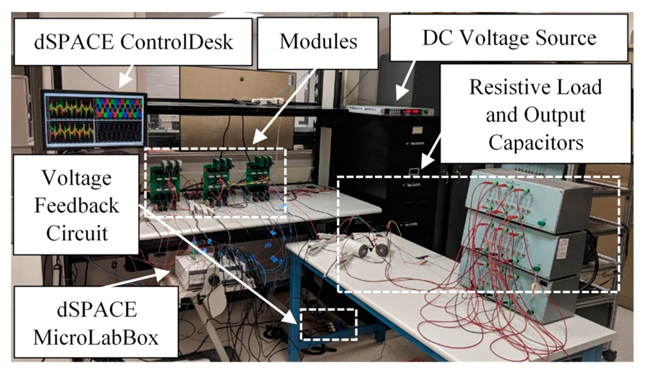
A three-module, proof-of-concept prototype was built and tested to verify the operation of the MCSI. Unlike previous MCSI prototypes, having custom-designed inductors that are strictly identical was not required for proper operation of the converter [11]. In fact, the inductors used in the prototype are off-the-shelf inductors with tolerance [18]. The unidirectional switches used in the modules are realized by connecting a SiC diode in series with an IGBT. The modified LS-SPWM, CBA, and data acquisition were implemented in a dSPACE MicroLabBox. All the measured voltages and currents were sent to dSPACE ControlDesk and then plotted using Matlab. Figure 8 shows a picture of the experimental setup. The rest of the prototype’s parameters are given in Table 2.
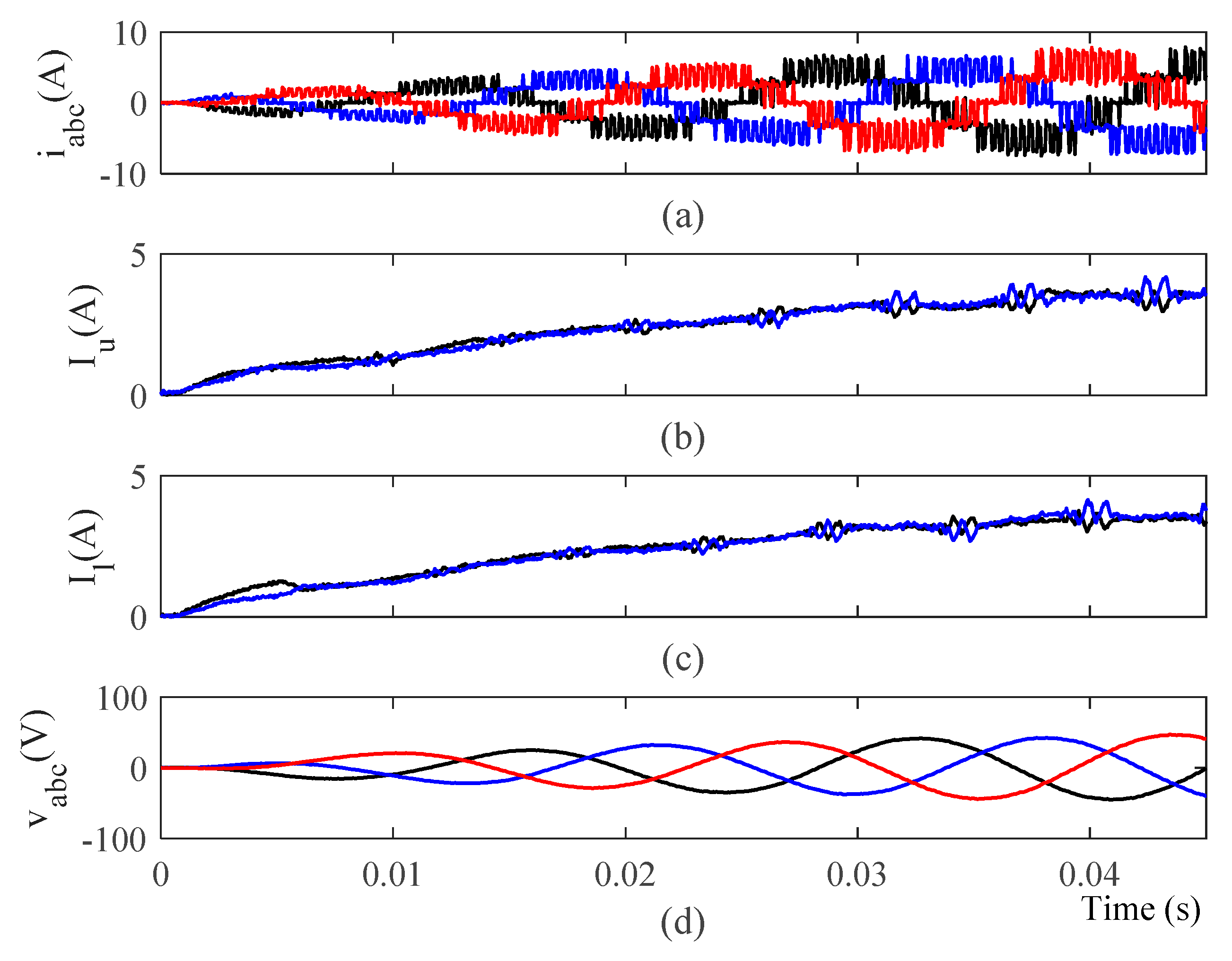
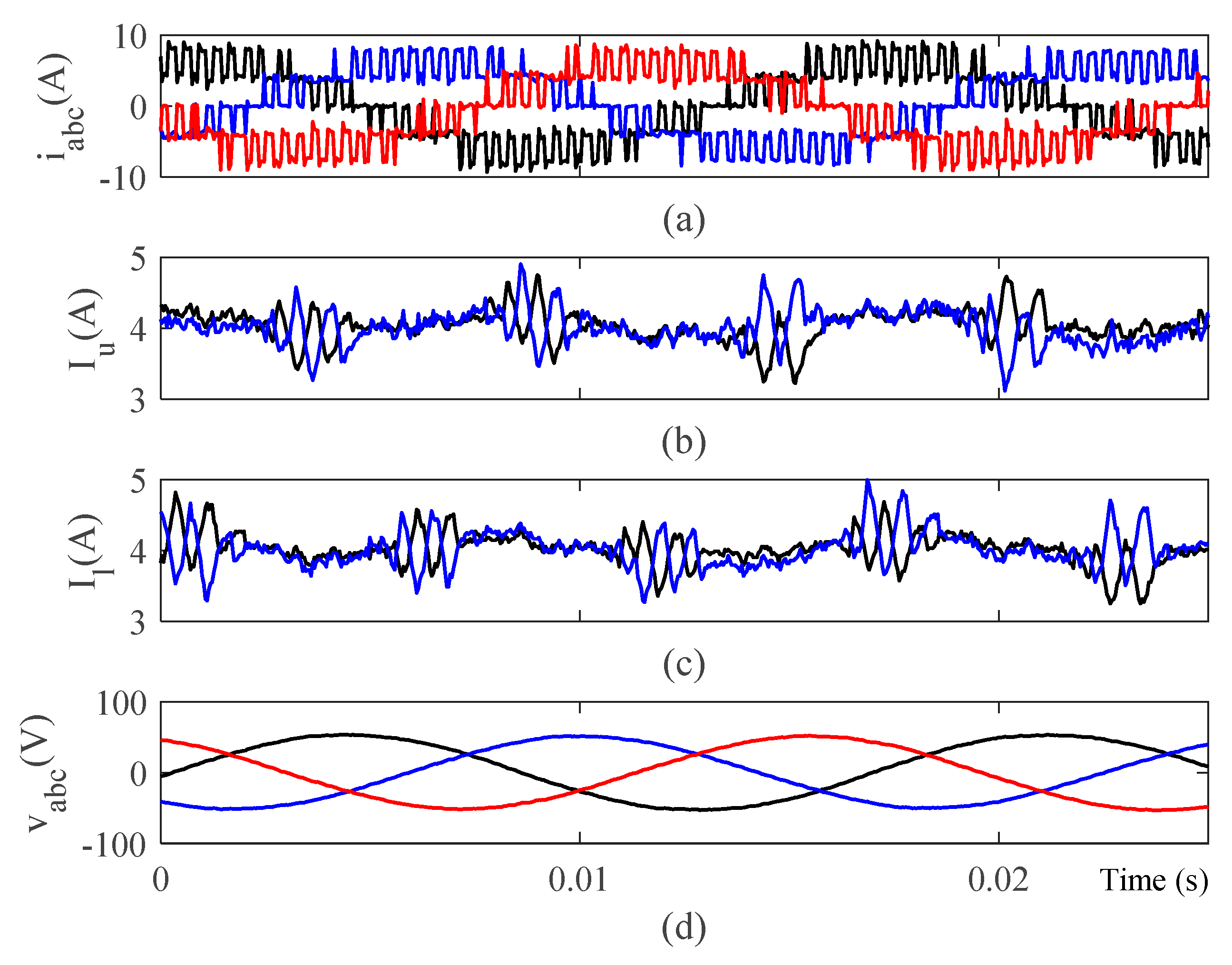
Initially, only two modules were used to create a five-level MCSI. The operation of the five-level MCSI during startup is shown in Figure 9. The CBA’s effectiveness is apparent in Figure 9b,c; the instantaneous values of the sharing inductors’ currents remained close to each other during startup. Figure 10 shows the same quantities under steady-state conditions. The CBA’s efforts can be observed in Figure 10b,c. When the output current of any phase is at its positive peak, referred to as odd intervals in Section 3, the upper sharing inductors experience similar , because they are connected to the same phase. On the other hand, the lower sharing inductors’ currents are changing at various rates, which shows the CBA’s effort to balance the inductors’ currents. When the output current of any phase is at its negative peak, the same phenomenon is reversed, changes are more apparent in the upper inductor’s currents.
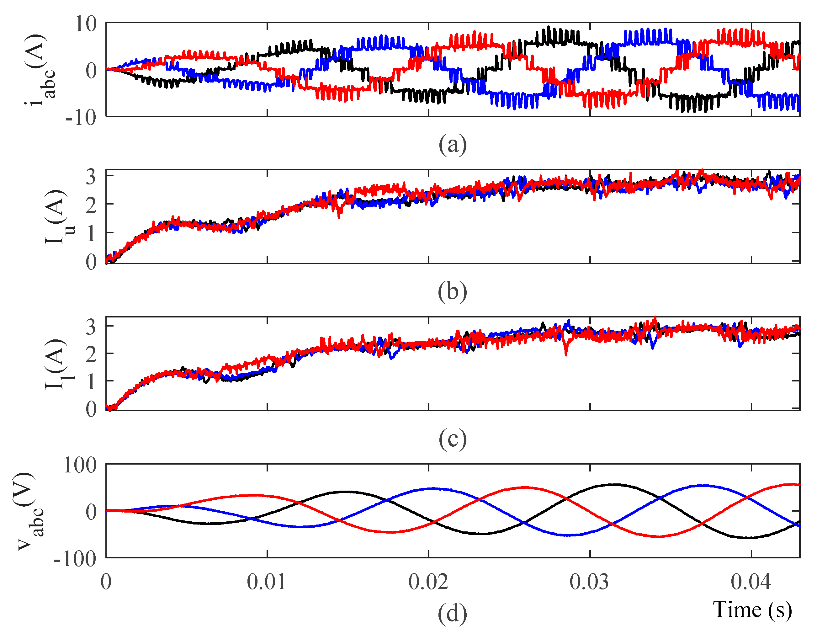
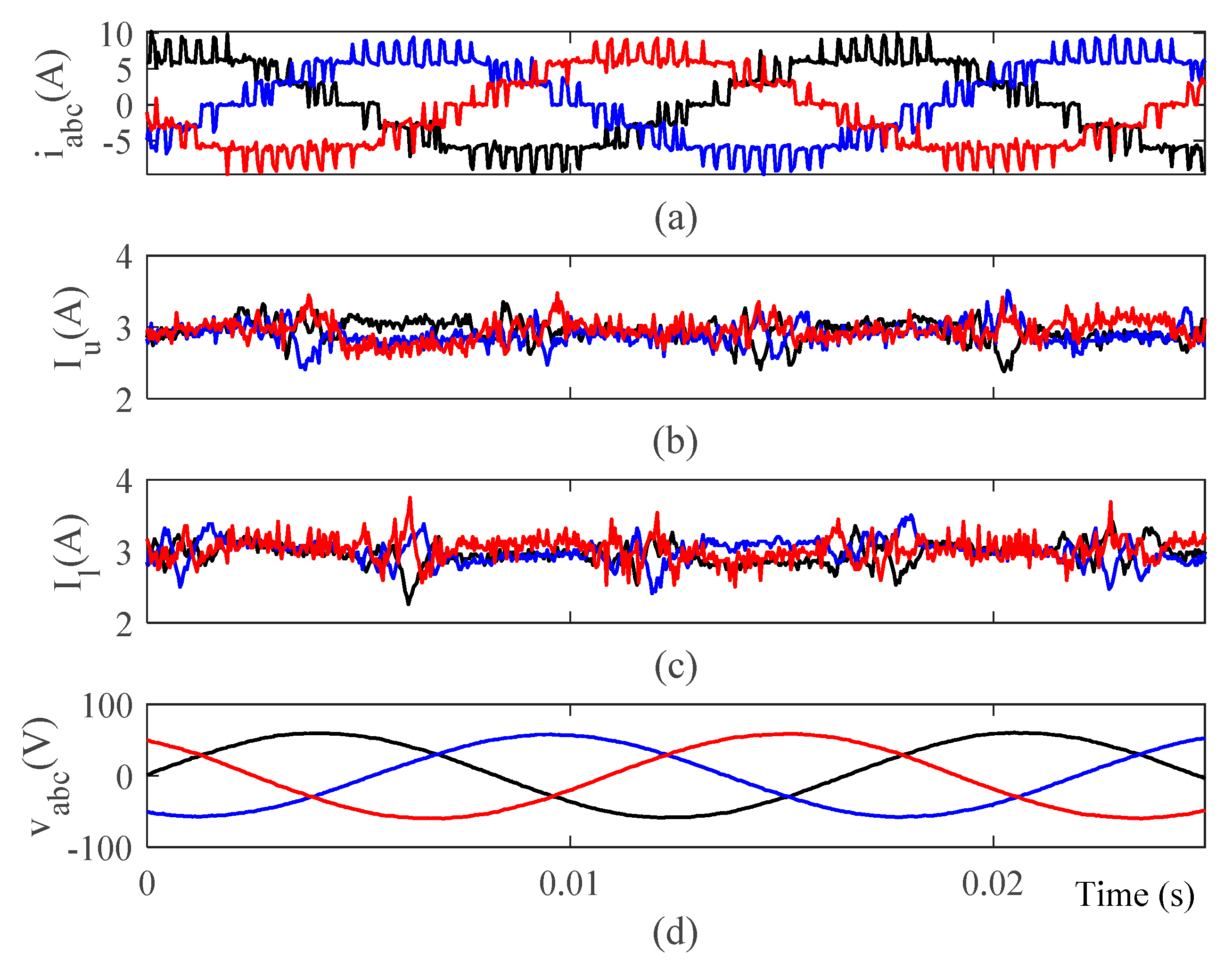
For further testing and verification, the third module of the prototype was activated to enable a seven-level operation. All the key waveforms of the seven-level MCSI during startup and steady-state operating conditions are presented in Figure 11 and Figure 12, respectively. Further demonstration of the effectiveness of the CBA is shown in Figure 12b,c.
5. Conclusions
A solution to the current balancing problem in voltage fed MCSIs was proposed in this paper. Unlike previous solutions [12,14], the CBA does not require any dedicated PI controllers; and it does not impose any alteration on the PWM carrier waveforms. Moreover, the CBA can be implemented in any MCSI, regardless of the number of levels. In addition, the modified LS-SPWM implementation in MCSIs was discussed in this paper. It was shown to have lower THD and compared to the PSC-SPWM. Although it was originally proposed for multilevel VSIs [16], it was never implemented in MCSIs. To validate the presented theoretical work, a proof-of-concept lab prototype was designed and tested. Experimental results for the five-level and seven-level cases were presented.
Author Contributions
Conceptualization, F.A. and M.G.S.; methodology, F.A. and M.G.S.; software, F.A.; validation, F.A.; formal analysis, F.A. and M.G.S.; investigation, F.A.; resources, F.A. and M.G.S.; data curation, F.A.; writing—original draft preparation, F.A.; writing—review and editing, F.A. and M.G.S.; visualization, F.A.; supervision, M.G.S.; project administration, M.G.S.; funding acquisition, F.A. and M.G.S. All authors have read and agreed to the published version of the manuscript.
Funding
This research received no external funding.
Conflicts of Interest
The authors declare no conflict of interest.
References
- Wu, B.; Narimani, M. High-Power Converters and AC Drives; Wiley; IEEE Press: Hoboken, NJ, USA, 2017; ISBN 978-1-119-15606-2. [Google Scholar]
- Moran, L.T.; Ziogas, P.D.; Joos, G. Analysis and design of a three-phase current source solid-state VAR compensator. IEEE Trans. Ind. Appl. 1989, 25, 356–365. [Google Scholar] [CrossRef]
- Stretch, N.; Kazerani, M.; Shatshat, R.E. A Current-Sourced Converter-Based HVDC Light Transmission System. In Proceedings of the 2006 IEEE International Symposium on Industrial Electronics, Montreal, QC, Canada, 9–13 July 2006; Volume 3, pp. 2001–2006. [Google Scholar]
- Gnanasambandam, K.; Rathore, A.K.; Edpuganti, A.; Srinivasan, D.; Rodriguez, J. Current-fed multilevel converters: An overview of circuit topologies, modulation techniques, and applications. IEEE Trans. Power Electron. 2016, 32, 3382–3401. [Google Scholar] [CrossRef]
- Jin, J.X.; Tang, Y.J.; Xiao, X.Y.; Du, B.X.; Wang, Q.L.; Wang, J.H.; Wang, S.H.; Bi, Y.F.; Zhu, J.G. HTS power devices and systems: Principles, characteristics, performance, and efficiency. IEEE Trans. Appl. Supercond. 2016, 26, 1–26. [Google Scholar] [CrossRef]
- Snitchler, G.; Gamble, B.; King, C.; Winn, P. 10 MW class superconductor wind turbine generators. IEEE Trans. Appl. Supercond. 2011, 21, 1089–1092. [Google Scholar] [CrossRef]
- Chen, X.Y.; Jin, J.X.; Xin, Y.; Shu, B.; Tang, C.L.; Zhu, Y.P.; Sun, R.M. Integrated SMES technology for modern power system and future smart grid. IEEE Trans. Appl. Supercond. 2014, 24, 1–5. [Google Scholar] [CrossRef]
- Bai, Z.; Zhang, Z. Conformation of multilevel current source converter topologies using the duality principle. IEEE Trans. Power Electron. 2008, 23, 2260–2267. [Google Scholar] [CrossRef]
- Xiong, Y.; Chen, D.; Yang, X.; Hu, C.; Zhang, Z. Analysis and experimentation of a new three-phase multilevel current-source inverter. In Proceedings of the 2004 IEEE 35th Annual Power Electronics Specialists Conference (IEEE Cat. No. 04CH37551), Aachen, Germany, 20–25 June 2004; Volume 1, pp. 548–551. [Google Scholar]
- Cossutta, P.; Aguirre, M.P.; Cao, A.; Raffo, S.; Valla, M.I. Single-stage fuel cell to grid interface with multilevel current-source inverters. IEEE Trans. Ind. Electron. 2015, 62, 5256–5264. [Google Scholar] [CrossRef]
- Aguirre, M.P.; Calvino, L.; Valla, M.I. Multilevel current-source inverter with FPGA control. IEEE Trans. Ind. Electron. 2012, 60, 3–10. [Google Scholar] [CrossRef]
- Aguirre, M.P.; Engelhardt, M.A.; Bracco, J.M.; Valla, M.I. Current balance control in a multilevel current source inverter. In Proceedings of the 2013 IEEE International Conference on Industrial Technology (ICIT), Cape Town, South Africa, 25–28 February 2013; pp. 1567–1572. [Google Scholar]
- Bai, Z.; Zhang, Z. Digital control technique for multi-module current source converter. In Proceedings of the 2008 IEEE International Conference on Industrial Technology, Chengdu, China, 21–24 April 2008; pp. 1–5. [Google Scholar]
- Cossutta, P.; Aguirre, M.P.; Engelhardt, M.A.; Valla, M.I. Control system to balance internal currents of a multilevel current-source inverter. IEEE Trans. Ind. Electron. 2017, 65, 2280–2288. [Google Scholar] [CrossRef]
- Espinoza, J.; Joos, G. On-line generation of gating signals for current source converter topologies. In Proceedings of the ISIE’93-Budapest: IEEE International Symposium on Industrial Electronics Conference Proceedings, Budapest, Hungary, 1–3 June 1993; pp. 674–678. [Google Scholar]
- Zhang, H.; Von Jouanne, A.; Dai, S.; Wallace, A.K.; Wang, F. Multilevel inverter modulation schemes to eliminate common-mode voltages. IEEE Trans. Ind. Appl. 2000, 36, 1645–1653. [Google Scholar]
- Holmes, D.G.; Lipo, T.A. Pulse width Modulation for Power Converters: Principles and Practice; John Wiley & Sons: Hoboken, NJ, USA, 2003; Volume 18. [Google Scholar]
- ERSE—Super Q. Available online: http://www.erseaudio.com/Products/SuperQCoilsAll/ESQ55-16-20000 (accessed on 31 December 2019).

Figure 2.
MCSI switching states: (a–c) Zero switching states, (d–i) Active switching states.

Figure 3.
Modified LS-SPWM: (a)Three-phase currents obtained using the conventional LS-SPWM, and , (b) Modified LS-SPWM, calculated using Equations (7)–(9).
Figure 3.
Modified LS-SPWM: (a)Three-phase currents obtained using the conventional LS-SPWM, and , (b) Modified LS-SPWM, calculated using Equations (7)–(9).

Figure 4.
PSC-SPWM [13], and .
Figure 4.
PSC-SPWM [13], and .

Figure 5.
Intervals highlighting the extreme values of a set of three-phase currents.

Figure 6.
Single current source inverter (CSI) module.

Figure 7.
A flow chart summarizing the current balancing algorithm (CBA).

Figure 8.
Experimental setup.

Figure 9.
Operation of the five-level MCSI during startup: (a) output current, (b) upper inductors’ currents, (c) lower inductors’ currents and (d) output voltage.
Figure 9.
Operation of the five-level MCSI during startup: (a) output current, (b) upper inductors’ currents, (c) lower inductors’ currents and (d) output voltage.

Figure 10.
Steady-state operation of the five-level MCSI: (a) output current, (b) upper inductors’ currents, (c) lower inductors’ currents and (d) output voltage.
Figure 10.
Steady-state operation of the five-level MCSI: (a) output current, (b) upper inductors’ currents, (c) lower inductors’ currents and (d) output voltage.

Figure 11.
Operation of the seven-level MCSI during startup: (a) output current, (b) upper inductors’ currents, (c) lower inductors’ currents, and (d) output voltage.
Figure 11.
Operation of the seven-level MCSI during startup: (a) output current, (b) upper inductors’ currents, (c) lower inductors’ currents, and (d) output voltage.

Figure 12.
Steady-state operation of the seven-level MCSI: (a) output current, (b) upper inductors’ currents, (c) lower inductors’ currents and (d) output voltage.
Figure 12.
Steady-state operation of the seven-level MCSI: (a) output current, (b) upper inductors’ currents, (c) lower inductors’ currents and (d) output voltage.


Table 1.
Zero state distribution in MCSI.
| Interval | ON Sau | ON Sal | ON Sbu | ON Sbl | ON Scu | ON Scl |
|---|---|---|---|---|---|---|
| I | 0 | 0 | ||||
| II | 0 | 0 | ||||
| III | 0 | 0 | ||||
| IV | 0 | 0 | ||||
| V | 0 | 0 | ||||
| VI | 0 | 0 |
Table 2.
Prototype parameters.
| Parameter | Value |
|---|---|
| Number of Modules | M = 3 |
| DC Voltage | 30 V |
| Modulation Index | (With 3rd harmonic injection) |
| AC Side Capacitors | (Delta-Connected) |
| Load | Y-Connected 28.57 Ω Resistors |
| Sharing Inductor Parameters (5% Tolerance) | |
| Switching Frequency | |
| Unidirectional Switch Parameters | IGBT: Infineon IRG7PH35UDPbF Diode: Cree C3D12065A |
| DSP | dSPACE MicroLabBox |
© 2020 by the authors. Licensee MDPI, Basel, Switzerland. This article is an open access article distributed under the terms and conditions of the Creative Commons Attribution (CC BY) license (http://creativecommons.org/licenses/by/4.0/).
Share and Cite
MDPI and ACS Style
Alskran, F.; Simões, M.G. Current Balancing Algorithm for Three-Phase Multilevel Current Source Inverters. Energies 2020, 13, 860. https://doi.org/10.3390/en13040860
AMA Style
Alskran F, Simões MG. Current Balancing Algorithm for Three-Phase Multilevel Current Source Inverters. Energies. 2020; 13(4):860. https://doi.org/10.3390/en13040860
Chicago/Turabian StyleAlskran, Faleh, and Marcelo Godoy Simões. 2020. "Current Balancing Algorithm for Three-Phase Multilevel Current Source Inverters" Energies 13, no. 4: 860. https://doi.org/10.3390/en13040860
Note that from the first issue of 2016, this journal uses article numbers instead of page numbers. See further details here.