Indirect Matrix Converter-Based Grid-Tied Photovoltaics System for Smart Grids


1
ETEC Department and MOBI Research Group, Vrije Universiteit Brussel (VUB), Pleinlaan 2, 1050 Brussels, Belgium
2
INESC-ID, Energy Systems, Power Electronics and Power Quality group, Instituto Superior Técnico, University of Lisbon, 1000-029 Lisbon, Portugal
3
BEAMS Energy Group, École polytechnique de Bruxelles, Université Libre de Bruxelles, 1050 Brussels, Belgium
4
Department of Electrical and Electronic Engineering, The University of Nottingham, Nottingham NG7 2QL, UK
*
Author to whom correspondence should be addressed.
†
This work was supported by the Belgian Fund for training in Research in Industry and in Agriculture (F.R.I.A.) and by national funds through Fundação para a Ciência e a Tecnologia, with project references UID/CEC/50021/2019 and PTDC/EEIEE/32550/2017.
Energies 2020, 13(20), 5405; https://doi.org/10.3390/en13205405
Submission received: 25 September 2020
/
Revised: 8 October 2020
/
Accepted: 9 October 2020
/
Published: 16 October 2020
(This article belongs to the Special Issue Electrical Engineering for Sustainable and Renewable Energy)
Abstract
:This paper proposes an Indirect Matrix Converter (IMC)-based grid-tied Photovoltaic (PV) system for Smart Grids (SGs). The PV array injects current in the ‘dc link’ of the IMC through an inductive link, and is connected to the SG with shunt and series connections, allowing for the compensation of current- and voltage-related Power Quality (PQ) issues, respectively, for the sensitive loads and the SG connection. A direct sliding mode-based controller is proposed to guarantee nearly sinusoidal currents in the connection to the SG, and sinusoidal voltages guaranteeing compliance with international standards, when supplying the sensitive loads. Additionally, a novel control approach for the ‘dc link’ voltage is synthesised to allow for the control of both the PV array current and the power flow to the SG. To guarantee the semiconductors safe commutation an asynchronous commutation strategy is derived. Simulation and experimental results show that the proposed system significantly improves PQ in the SG, minimizing the total harmonic distortion of the currents injected in the SG, and guaranteeing the quality of the voltage supplied to the sensitive loads, even in the occurrence of voltage sags or overvoltages.

1. Introduction
The increasing penetration of Distributed Energy Resources (DERs), in particular Photovoltaic (PV) systems in the Low-Voltage (LV) and Medium-Voltage (MV) grid and the growing use of power-electronics based equipment are leading to new challenges for distribution system operators (DSOs) and critical consumers. These include Power Quality (PQ) issues such as low-order current harmonics, due to the use of non-linear loads, resulting in additional losses and voltage distortion in the point of connection to the grid (Point of Common Coupling—PCC) [1]. Also, voltage-related disturbances on the LV grid, such as voltage sag/swell and permanent undervoltage/overvoltage, are PQ issues that are of great concern for most critical loads, as they may lead to equipment malfunction and degradation, short-time interruptions and an overall decrease in efficiency [2,3,4,5].
In this context, energy management schemes for integrating different DERs, such as PV and energy storage systems, into Smart Grids (SGs) with conventional and controllable loads have been proposed [6,7], and new concepts such as demand side management have emerged, whereby consumers can modify their energy demand (e.g., through financial incentives or changes in consumption habits), becoming an active part of the energy management process. As for DERs, the active and, to a lesser extent, reactive power production should be controllable to increase the flexibility of the system, solving some PQ issues, and working towards an enhanced SG [8,9].
Following these emerging challenges, international standards have been proposed and harmonised to guarantee PQ enhancement, and to improve overall grid performance [8]. In particular, PV inverters are expected to minimise their harmonic impact on the grid to guarantee compliance with the current harmonic limitations in the LV grid, set by standard IEC 61000-3-2 [3,10]. Also, the distribution voltage quality is regulated by standards IEC 61000-3-3 and EN 50160, which bound the voltage rms value and harmonic content [2,11].
In order to comply with the abovementioned regulations and limit the PQ issues on the LV grid, new PV inverter topologies and control methods have been proposed to act as Active Power Filters (APFs) with current and voltage compensation, overcoming the limited possibilities of passive filtering and guaranteeing a better integration into the emerging SG [7,12]. The common shunt-connected PV inverters can be used to compensate low-order current harmonics produced by non-linear loads. This has been proposed either with load current measurement [13] or with grid current control, using Voltage-Source Inverter (VSI)-based [14] or Current-Source Inverter (CSI)-based topologies [15]. Grid voltage sag/swell and undervoltage/overvoltage can also be mitigated at the PCC to a certain extent using active power control and reactive power compensation [16,17,18]. However, the voltage compensation using a shunt converter is limited through the network impedance [9]; thus, alternative methods have been proposed with additional inverters or capacitor banks [19], or a series-connected inverter instead [9,20]. With the latter solution, the PV system injects series voltages on the grid to control the voltages at the PCC, where the sensitive loads are connected. This naturally leads to a Unified Power Quality Conditioner (UPQC) topology including current and voltage compensation with shunt and series converters, respectively [1,5,21,22,23].
In this paper the use of a UPQC with integrated PV array (PV-UPQC) is investigated [24,25,26]. Instead of the more common shunt and series Voltage-Source Converter (VSCs) an Indirect Matrix Converters (IMC) is proposed to form the UPQC, guaranteeing improved compactness [27] and higher reliability [28] that result from the absence of a bulky dc link electrolytic capacitor [12,27,29,30] or an additional film capacitor with increased system complexity. Even though the IMC lacks voltage-step-up capability (input/output ratio of 0.86 for sinusoidal modulation) [28], it is an advantage in the proposed PV-UPQC as the PV array voltage is usually lower than the grid voltage. The shunt part of the IMC acts as a voltage-step-up converter with a minimum transfer ratio of 1.155, with no need for an additional dc/dc converter and full operating point range as long as the PV system is sized so that the open circuit voltage does not exceed the limit set by the converter modulation [15,31]. This limitation in PV array voltage may increase the system losses but also reduces the safety issues and allows for lower power operation.
This paper describes advances in the technology of SG-connected PV systems by proposing a novel IMC-based PV-UPQC system where the PV array injects current into the ’virtual dc link’ of the IMC. The three-phase PV-UPQC system is modelled in Section 2. Then, the PV-UPQC controllers are investigated in Section 3 and Section 4 for the series converter to have adequate voltage at the PCC and the shunt converter to guarantee quasi sinusoidal grid currents, respectively. A novel modulation method for the ‘dc link’ voltage is proposed in Section 4, allowing for a wider selection of switching vectors and better control of the grid currents while ensuring the proper operation of the IMC with positive ‘dc link’ voltage. The laboratory setup is detailed in Section 5, and a novel switching strategy is proposed to guarantee that the ‘dc link’ voltage is always positive. Simulation and experimental results confirm that the PV system operates according to the SG integration requirements.
2. Model of the Grid-Tied PV-UPQC System
The proposed PV-UPQC system is presented in Figure 1. The shunt converter compensates the low-order current harmonics injected by the sensitive non-linear loads and guarantee reduced current at the point of connection to the SG [14]. The series converter produces compensation voltages for supplying the sensitive loads with adequate voltages at the PCC, mitigating voltage PQ issues [9]. The UPQC is formed with an IMC consisting of a VSC (series converter) and a 3×2 Matrix Converter (MC) (shunt converter), which are connected through a direct ‘dc link’ with switched current and voltage [27], into which the PV array injects current. Therefore, the PV array is primarily used to provide power to the load and the system configuration allows adding enhanced shunt and series active filtering functionalities. This topology can be extended with any DC source replacing the PV arrays, however with adjusted control and interfacing power electronics.
2.1. Shunt Converter
The shunt converter is characterised by the switching matrix with the respective condition on the switching states :
The ‘dc link’ voltage is obtained from the shunt converter ac voltages : Similarly, the converter ac currents are obtained from the ‘dc link’ current :
The switching states of the shunt converter (numbered 1 to 9) are presented in Table 1, with the corresponding current ac vectors in function of the shunt converter dc current.
A time-invariant state-space model of the shunt side of the UPQC is obtained in the grid-synchronised frame, neglecting the damping resistors:
where are the grid currents, the capacitor line-to-line voltages, the load voltages, the converter ac currents (generated as functions of the converter dc current) and the grid voltage pulsation.
2.2. Series Converter
In the series connection, the converter is characterised by the switching matrix (3), where :
The series converter dc current is obtained from the converter ac currents :
and the series converter ac voltages are expressed with the ‘dc link’ voltage :
The detailed switching states of the series converter (numbered I to VIII) are presented in Table 2, with the corresponding voltage ac vectors in function of the ‘dc link’ voltage generated by the shunt converter.
The series converter is modelled by the following alpha-beta frame equations:
where are the series converter ac currents, the capacitor line-to-line voltages, the series transformer currents and the converter ac voltages (generated as functions of the ‘dc link’ voltage).
Similarly to the shunt converter, the equations are also obtained in the frame:
where are the series converter ac currents, the capacitor line-to-line voltages, the series transformer currents and the converter ac voltages. These equations will be further used to design the PV-UPQC controllers.
2.3. PV System
The PV system is governed by the PV array characteristics and the dc inductor equation:
where is the ‘dc link’ voltage, and the PV array voltage and current, and the PV array dc inductance. The PV array current adds up to the series converter dc current such that the shunt converter dc current is .
3. Control of the Shunt Converter
The shunt converter is used to guarantee quasi sinusoidal currents on the SG and also determines the ‘dc link’ voltage that can be used for controlling the PV array operating point, considering that the array is directly connected to the converter terminals.
3.1. Control of the SG Currents
Direct sliding mode controllers are used for the SG currents [32,33,34] and generate the switching vectors for the shunt converter. From Figure 1, the SG currents can be controlled acting on the IMC shunt currents [15], as , the load currents being considered as a perturbation. Considering the second-order dynamics of the IMC shunt currents, the sliding surfaces [15,32] for and will be one order lower, and can be expressed as a linear combination of the current errors and their time derivatives:
where and are positive-valued adjustable gains, the d- and q-axis grid currents, and the respective errors are
The reference values are set to produce sinusoidal currents and mitigate harmonics on the SG, despite non-linear loads connected to the PCC. The d-axis current reference is generated from the PV array current controller (see Figure 1), while the q-axis current reference is set to control the Power Factor (PF).
According to the shunt filter state-space Equations (2), the grid currents can be controlled by acting on the converter ac currents [15]. Therefore, these currents should be applied to modify the time derivative of the sliding surfaces and to meet the stability criterion
based on the sliding mode variables produced by two- and three-level hysteresis comparators for and , respectively. The criteria to choose the state-space vectors should be:
- If () then and a vector that decreases should be chosen
- If () then and a vector that does not significantly modify should be chosen
- If () then and a vector that increases should be chosen
Considering these criteria, the space vectors should be chosen to avoid short-circuits through the series converter free-wheeling diodes, thus guaranteeing that the ‘dc link’ voltage is higher than or equal to zero.
The grid voltages within a single grid period are shown in Figure 2 with a decomposition in 12 voltage zones (from to ), also representing the ‘dc link’ voltage in function of the different switching vectors (neglecting the voltage drops in the shunt filter inductors). In the odd zones, only two non-zero vectors guarantee a positive ‘dc link’ voltage while there are three in the even zones. For example, in zone (see Figure 2), only and can be applied by the shunt converter to the ‘dc link’, which corresponds to vectors 1 and 2, respectively (see Table 1). All the non-zero vectors that can be applied in the different zones are gathered in Table 3.
The space vectors are also shown in Figure 3a in the stationary frame, considering that the current (Figure 1) is positive, as it will be mainly set by the PV array power. Also, the same decomposition in voltage zones as in Figure 2 is represented, and in each voltage zone the d- and q-axis converter ac currents and , respectively, are controlled by selecting the most appropriate shunt converter switching vector: one of the non-zero vectors or a zero vector. An example is given in Figure 3b for zone where the space vectors that are allowed (1,2,6) are represented. All selectable non-zero vectors would increase , while a zero vector (7,8,9) must be used to decrease it. Vectors 2 and 6 would increase and decrease , respectively, while vector 1 would keep it nearly constant.
The switching vector is selected among the possibilities identified in Table 3, in function of the control variables and the voltage zone; this results in the selection in Table 4. The ‘dc link’ current must remain positive for control logics, which is the case as long as the PV array current compensates the switched component from the series converter.
3.2. PV Array Current Control
The PV array is directly connected to the IMC ‘dc link’, therefore the switching vector applied to the converter has an impact on the PV array operating point. In particular, the PV array current can be controlled provided that the ‘dc link’ voltage is either higher or lower than the PV array voltage (depending on the switching vector selected). Considering the positive ‘dc link’ voltage restrictions in the selection of vectors (Table 1 and Table 3), is guaranteed to be lower than only when applying zero vectors, which is thus a necessary condition for controlling . In order to guarantee that is higher than otherwise, for non-zero vectors, the PV array must be sized so that the open circuit voltage meets the following condition: (see Figure 2 and Table 3).
As shown in Figure 1, the Proportional-Integral (PI) controller of the PV array current generates the d-axis grid current reference . The block diagram in Figure 4 is used to size the PI controller proportional and integral gains and , respectively.
The shunt converter transfer function that links the dc and ac power flows in the system is
where is the average delay introduced by the shunt converter and grid-side filter, the voltage at the input of the converter averaged over a switching period and the transfer function gain determined from the average power balance of the system.
4. Control of the Load Voltages
To guarantee sinusoidal load voltages with preset rms value the voltages at the series transformer converter-side terminals (primary) should be controlled, through the control of the series converter ac currents .
4.1. Series Converter ac Current Control
Direct sliding mode controllers are used for the converter ac currents [32], generating the switching vectors for the series converter. The dynamics of the converter ac currents are directly dependent on the converter ac voltages , as shown in the state-space Equation (6).
As the converter ac currents have a strong relative degree of one, the sliding surfaces will depend directly on the current errors (14) [32].
where is a positive-valued adjustable gain and the - and -axis converter ac currents.
According to (6), the currents can be controlled directly by the converter ac voltages . Three-level hysteresis comparators are used for producing the control variables that will be used to choose the most adequate switching combination to control the currents .
The ac voltage vectors of the series converter are defined in Table 2 in function of the switching states and represented in Figure 5 in the frame. The selection of the space vector to apply is shown in Figure 5 in function of the sliding variables. For example, vector III decreases and increases —it is thus chosen when . The ‘dc link’ voltage generated by the shunt converter periodically takes null values, which may increase the ripple of the series converter ac currents but does not alter the control logics.
4.2. Series Voltage Control
As shown in Figure 1, the references of the -axis capacitor voltages are obtained from the error between the balanced grid voltages and the references of the load voltages and , considering the turns ratio n of the series transformer: .
The converter ac currents are linked to the series voltages and series transformer currents using the state-space Equation (7). The series transformer currents can account for the perturbation from the grid currents and they are replaced by intermediate variables. When isolating the converter ac current references , it comes:
where the series voltages are directly considered and and represent the perturbation from the grid currents. These variables are obtained from the control of the capacitor voltages, using the ITAE criterion to size the PI controller. Considering a switching frequency of approximately 2 , the proportional and integral gains are and , respectively [35].
5. Simulation and Experimental Results
The proposed PV-UPQC (Figure 1) has been simulated in the MATLAB/Simulink environment and implemented in the laboratory (Figure 6). The setup is here detailed, in particular the switching procedure of the shunt converter to avoid negative ‘dc link’ voltage.
5.1. Setup Description
The experimental setup is shown in Figure 6 and the parameter values are presented in Table 5. The fast-prototyping software and hardware DS1103 (dSPACE GmbH, 33102 Paderborn, Germany) (c) is used with its ControlDesk interface to run the experiments at a sample time .
The IMC is built by connecting a VSC module from Semiteach (series converter, (2)) with a MC prototype (shunt converter, (1)). In order to allow for a direct ‘dc link’ connection (f) and the use of a switched ‘dc link’ voltage, the VSC electrolytic and snubber capacitors were removed.
The PV array emulator is built with a programmable power supply (maximum values of , 360 and 15 ) and connected to the ‘dc link’ (b). The system operates at rated conditions, with and .
The switching signals are sent to the converters from dSPACE (c) and an FPGA (e) is used to guarantee the safe switching of the MC bidirectional switches. The series transformer (3) has a turns ratio of 3.31 from primary (converter-side) to secondary (grid-side) and has been designed for a maximum compensation of 25% of the grid voltages. The 250 non-linear load is built with a three-phase full-bridge diode rectifier (9) with capacitive dc filtering and a resistive load (8), which generates high harmonic currents and is representative of electronic industrial equipment.
5.2. Semiconductors Switching Strategy
The shunt converter is controlled to switch between the non-zero vectors in Table 3 and any of the three zero vectors. The states of the switches of the MC prototype are modified sequentially due to the pre-built 4-step commutation process and when the conducting switches on both the upper and lower branches differ during a transition, an intermediate switching vector is applied to the converter. This may be a problem, as this intermediate switching vector may result in a negative voltage in the virtual dc link, thus leading to a short-circuit through the series converter diodes. For example, in zone , vectors 2 and 7 have different conducting switches on both the upper and lower branches (see Table 1). In order to switch only one branch at a time, the sequence would be –– on the upper branch and –– on the lower branch. This would result in vectors 2–3–7. However, from Table 1, in zone , vector 3 is not allowed as it would produce an unacceptable negative ‘dc link’ voltage spike.
To solve this problem, a new switching strategy is proposed considering that at least two zero vectors must be available in each zone to guarantee a smooth operation when changing zone. The available non-zero vectors in Table 3 together with the two zero vectors are shown in Figure 7a for voltage zone . The vectors that can be applied successively are linked such that for example a transition from vector 1 to 8 is done by applying first vector 6 and then vector 8. The same example is given for zone in Figure 7b; the transition from vector 2 to 7 is done by first applying vector 1 and then 7. This can be generalised for the 12 voltage zones.
5.3. Results
Simulation and experimental results are obtained under different operating conditions: (1) no-load; (2) linear and non-linear load; (3) voltage sag and swell with no load. Different power flows are considered, with either active power flowing from the SG () or to the SG (). Ideal switches are used to model the MC for faster simulations.
5.3.1. No-Load Conditions
The system is operated at rated conditions, with all the PV array power flowing to the SG.
The ‘dc link’ variables obtained with simulation and experiments are shown in Figure 8a,d, respectively. In both results, the ‘dc link’ voltage is never negative, showing that the IMC setup is working properly. Also, the pulse of six times the grid frequency, which is characteristic of three-phase IMCs, is clearly visible. The higher variation in the experimental voltage results from stray inductance dynamics and non-ideal semiconductor switching characteristics that have not been considered in simulation. Both in simulation and experimental results, the PV array current is controlled to its reference ( ) and the shunt converter dc current has a switched component coming from the series converter.
One grid line-to-ground voltage and the corresponding line current flowing to the SG are shown in Figure 8b,e for simulation and experimental results, respectively, and the PF is nearly unitary. In the experimental results the grid voltage presents 5th harmonics, which is common in non-ideal grids. The experimental grid line current presents a slightly higher ripple than in simulation, which is mainly due to the non-modelled switching characteristics of power electronic semiconductors.
The dynamic behaviour of the PV array current control is observed with irradiance steps between and , for worst case scenario. The simulation and experimental results in Figure 8c,f, respectively, show a variation of about 10% in the PV array current operating point. The grid currents (same figures) present a similar amplitude variation.
5.3.2. Load Conditions
A 250 non-linear load (see Section 5.1) is first connected at the PCC to observe the low-order harmonic compensation from the shunt converter (). The simulation and experimental results (for phase a) are shown in Figure 9: the non-linear load current , the shunt converter ac current and the grid current .
The load currents present high 5th and 7th harmonics that are compensated by the shunt currents such that nearly sinusoidal currents are injected in the grid. This is confirmed by the results where the low-order harmonic content of the converter ac line current is clearly visible. In particular, in the laboratory the Total Harmonic Distortion (THD) of the load line current is 43.53%, with harmonics 5 and 7 of 39.12% and 14.91% of the fundamental, respectively, and the THD of the grid line current is 10.83%. A PF of 0.997 is measured, as shown in Figure 9c with the SG line-to-ground voltage and line current nearly in phase. The simulation currents present similar harmonic contents.
A second test is performed connecting an additional resistive load of 2 (), so that the grid is providing power to the load as the PV power is not sufficient anymore. The grid, shunt and load currents are shown in Figure 10a; the current flows from the grid to the load so it is in phase opposition with the grid voltages. Also, the instantaneous active power flowing through the system is shown in Figure 10b with the 300 oscillation from the PV array power for compensating the load power as no storage components are used for that purpose. The reactive power results in Figure 10c show that the harmonics compensation comes from the shunt converter and the PF on the SG is equal to .
A potential decrease in PV power has no impact on the PQ compensation as the PV current provides primarily the fundamental harmonic of the load current.
5.3.3. Voltage Sag/Swell Conditions
Simulation results for a 10% voltage sag with 10 degree phase-shift are shown in Figure 11a, in no load conditions. The grid currents and PCC voltages are controlled to be in phase with the grid voltages at all time in order to guarantee a nearly unitary PF even during voltage sags. The results for a zero phase-shift sag of 15% and swell of 10% to the balanced grid voltages are shown in Figure 11b, in no load conditions. The corresponding experimental results are shown in Figure 11c,d, respectively. The series transformer injects voltages that are in phase with the grid line-to-ground voltages during the sag and in phase opposition during the swell, to compensate the grid voltages. The load voltages have bounded rms values.
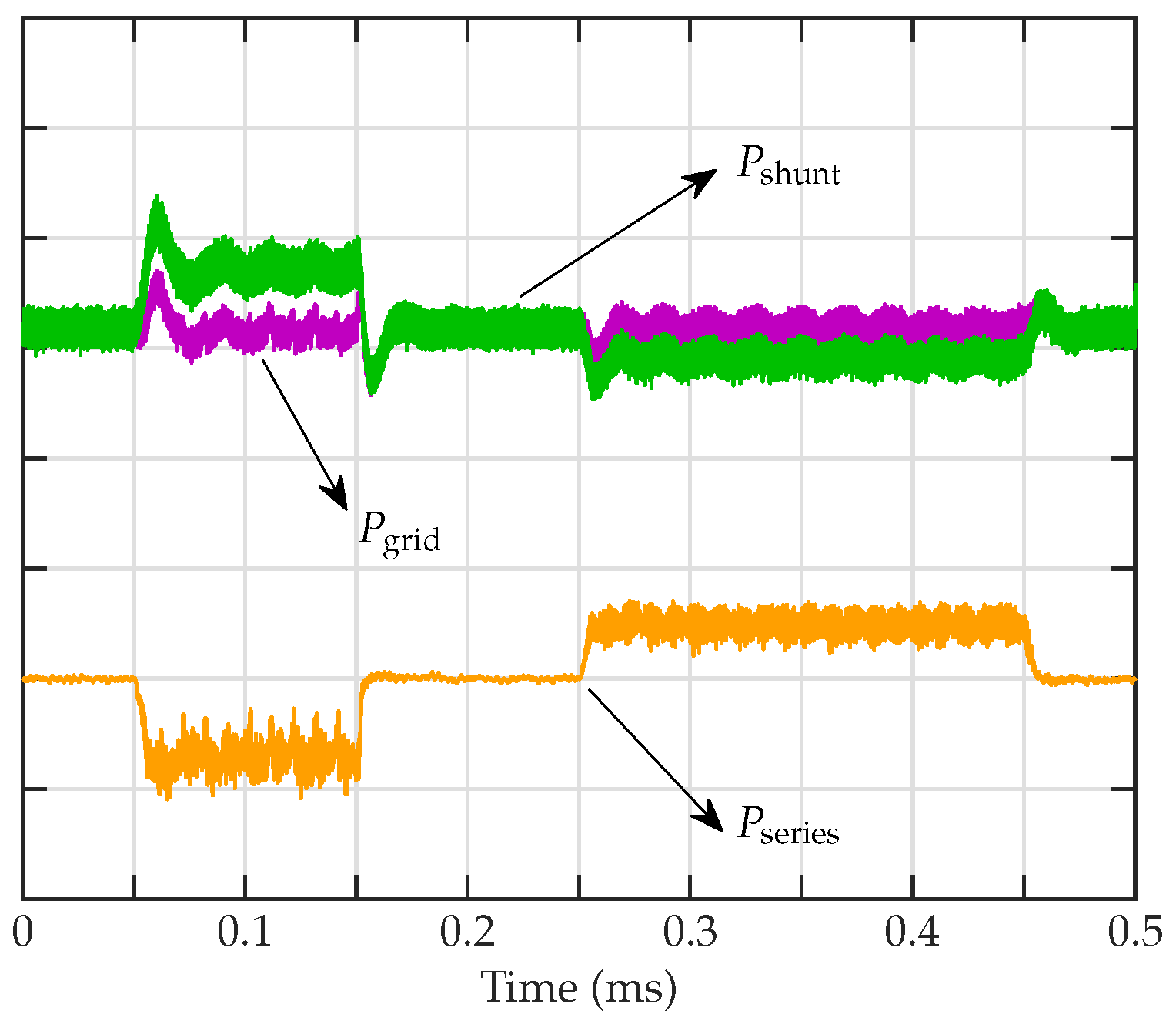
Also, the instantaneous power is shown in Figure 12. Considering that here the PV array injects active power on the grid (), active power is flowing from the grid to the ‘dc link’ through the series converter and from the ‘dc link’ to the grid through the shunt converter. During voltage swell, active power is flowing through the series converter to the grid. The active power injected on the SG remains constant, with small transients due to the ‘dc link’ controller dynamics. The flows are reversed in case active power is flowing from the grid to the load in standard conditions ().
6. Conclusions
A new topology to integrate a PV system into a SG has been investigated. The PV array injects current into the ‘dc link’ of an IMC that provides series and shunt connections to improve PQ in the SG. The proposed PV-UPQC guarantees the compensation of both low-order current harmonics produced by non-linear loads, to inject quasi sinusoidal currents in the SG, and grid voltage sag/swell and undervoltage/overvoltage, to supply the sensitive loads with bounded rms values. Direct sliding mode controllers have been used to guarantee fast dynamic response, and a novel asynchronous ‘dc link’ voltage modulation (shunt converter) has been proposed to guarantee a positive voltage on the series converter dc side and control both the SG currents and the PV array power. Simulation and experimental results validate the enhanced PQ compensation functionality of the system: the SG currents low-order harmonics are mitigated when sensitive non-linear loads are used and voltage sags/swells up to 15% are compensated to supply these loads.
Author Contributions
Conceptualisation, T.G., S.F.P., J.G. and P.W.; methodology, T.G., S.F.P., J.G. and P.W.; software, T.G, S.F.P. and J.G.; validation, T.G. and S.F.P.; formal analysis, T.G., S.F.P., J.G. and P.W.; investigation, T.G., S.F.P., J.G. and P.W.; data curation, T.G.; writing—original draft preparation, T.G.; writing—review and editing, T.G., S.F.P., J.G. and P.W.; supervision, S.F.P., J.G. and P.W.; project administration, J.G.; funding acquisition, S.F.P. and J.G. All authors have read and agreed to the published version of the manuscript.
Funding
This research project was funded by the Belgian Fund for training in Research in Industry and in Agriculture (F.R.I.A.). This work was supported by national funds through Fundação para a Ciência e a Tecnologia, with project references UID/CEC/50021/2019 and PTDC/EEIEE/32550/2017.
Conflicts of Interest
The authors declare no conflict of interest.
References
- Hafezi, H.; D’Antona, G.; Dedè, A.; Della Giustina, D.; Faranda, R.; Massa, G. Power Quality Conditioning in LV Distribution Networks: Results by Field Demonstration. IEEE Trans. Smart Grid 2017, 8, 418–427. [Google Scholar] [CrossRef]
- Singh, B.; Chandra, A.; Al-Haddad, K. Power Quality: Problems and Mitigation Techniques; Wiley: Hoboken, NJ, USA, 2015; p. 582. [Google Scholar]
- Asrari, A.; Wu, T.; Lotfifard, S. The Impacts of Distributed Energy Sources on Distribution Network Reconfiguration. IEEE Trans. Energy Convers. 2016, 31, 606–613. [Google Scholar] [CrossRef]
- Torquato, R.; Salles, D.; Pereira, C.O.; Meira, P.C.M.; Freitas, W. A Comprehensive Assessment of PV Hosting Capacity on Low-Voltage Distribution Systems. IEEE Trans. Power Deliv. 2018, 33, 1002–1012. [Google Scholar] [CrossRef]
- Yang, D.; Ma, Z.; Gao, X.; Ma, Z.; Cui, E. Control strategy of intergrated photovoltaic-UPQC System for DC-Bus voltage stability and voltage sags compensation. Energies 2019, 12, 4009. [Google Scholar] [CrossRef] [Green Version]
- Tushar, W.; Chai, B.; Yuen, C.; Smith, D.B.; Wood, K.L.; Yang, Z.; Poor, H.V. Three-Party Energy Management With Distributed Energy Resources in Smart Grid. IEEE Trans. Ind. Electron. 2015, 62, 2487–2498. [Google Scholar] [CrossRef] [Green Version]
- Ahmad, A.; Hassan, N.U. Smart Grid as a Solution for Renewable and Efficient Energy; IGI Global: Hershey, PA, USA, 2016; p. 415. [Google Scholar]
- Bacha, S.; Picault, D.; Burger, B.; Etxeberria-Otadui, I.; Martins, J. Photovoltaics in Microgrids: An overview of grid integration and energy management aspects. Ind. Electron. Mag. 2015, 33–46. [Google Scholar] [CrossRef]
- Saadat, N.; Choi, S.S.; Vilathgamuwa, D.M. A series-connected photovoltaic distributed generator capable of enhancing power quality. IEEE Trans. Energy Convers. 2013, 28, 1026–1035. [Google Scholar] [CrossRef]
- Teodorescu, R.; Liserre, M.; Rodriguez, P. Grid Converters for Photovoltaic and Wind Power Systems; Wiley: Hoboken, NJ, USA, 2011; p. 398. [Google Scholar]
- Tang, C.Y.; Chen, Y.T.; Chen, Y.M. PV Power System With Multi-Mode Operation and Low-Voltage Ride-Through Capability. IEEE Trans. Ind. Electron. 2015, 62, 7524–7533. [Google Scholar] [CrossRef]
- Szczesniak, P.; Kaniewski, J. Power electronics converters without DC energy storage in the future electrical power network. Electr. Power Syst. Res. 2015, 194–207. [Google Scholar] [CrossRef]
- Chilipi, R.R.; Sayari, N.A.; Beig, A.R.; Hosani, K.A. A Multitasking Control Algorithm for Grid-Connected Inverters in Distributed Generation Applications Using Adaptive Noise Cancellation Filters. IEEE Trans. Energy Convers. 2016, 31, 714–727. [Google Scholar] [CrossRef]
- Munir, M.; Li, Y. Residential distribution system harmonic compensation using PV interfacing inverter. IEEE Trans. Smart Grid 2013, 4, 816–827. [Google Scholar] [CrossRef]
- Geury, T.; Pinto, S.; Gyselinck, J. Current source inverter-based photovoltaic system with enhanced active filtering functionalities. IET Power Electron. 2015, 8, 2483–2491. [Google Scholar] [CrossRef] [Green Version]
- Ghanbari, T.; Farjah, E.; Naseri, F. Power quality improvement of radial feeders using an efficient method. Electric Power Syst. Res. 2018, 163, 140–153. [Google Scholar] [CrossRef]
- Gayatri, M.; Parimi, A.; Pavan Kumar, A. A review of reactive power compensation techniques in microgrids. Renew. Sustain. Energy Rev. 2018, 81, 1030–1036. [Google Scholar] [CrossRef]
- Ali, M.S.; Haque, M.M.; Wolfs, P. A review of topological ordering based voltage rise mitigation methods for LV distribution networks with high levels of photovoltaic penetration. Renew. Sustain. Energy Rev. 2019, 103, 463–476. [Google Scholar] [CrossRef]
- Kumar, M.; Mishra, M.; Kumar, C. A Grid-Connected Dual Voltage Source Inverter with Power Quality Improvement Features. IEEE Trans. Sustain. Energy 2015, 6, 482–490. [Google Scholar] [CrossRef]
- Benali, A.; Khiat, M.; Allaoui, T.; Denaï, M. Power Quality Improvement and Low Voltage Ride Through Capability in Hybrid Wind-PV Farms Grid-Connected Using Dynamic Voltage Restorer. IEEE Access 2018, 6, 68634–68648. [Google Scholar] [CrossRef]
- Santos, R.; Cunha, J.; Mezaroba, M. A Simplified Control Technique for a Dual Unified Power Quality Conditioner. IEEE Trans. Ind. Electron. 2014, 61, 5851–5860. [Google Scholar] [CrossRef]
- Khadkikar, V. Enhancing electric power quality using UPQC: A comprehensive overview. IEEE Trans. Power Electron. 2012, 27, 2284–2297. [Google Scholar] [CrossRef]
- Muthuvel, K.; Vijayakumar, M. Solar PV sustained quasi Z-source network-based unified power quality conditioner for enhancement of power quality. Energies 2020, 13, 2657. [Google Scholar] [CrossRef]
- Geury, T.; Pinto, S.; Gyselinck, J.; Wheeler, P. An Indirect Matrix Converter-based Unified Power Quality Conditioner for a PV inverter with enhanced Power Quality functionality. In Proceedings of the 2015 IEEE Innovative Smart Grid Technologies—Asia (ISGT ASIA), Bangkok, Thailand, 3–6 November 2015; pp. 1–8. [Google Scholar] [CrossRef] [Green Version]
- Campanhol, L.; Silva, S.; Oliveira, A.; Bacon, V. Single-stage three-phase grid-tied pv system with universal filtering capability applied to DG systems and AC microgrids. IEEE Trans. Power Electron. 2017, 32, 9131–9142. [Google Scholar] [CrossRef]
- Devassy, S.; Singh, B. Design and Performance Analysis of Three Phase Solar PV integrated UPQC. IEEE Trans. Ind. Appl. 2018, 54, 73–81. [Google Scholar] [CrossRef]
- Peña, R.; Cárdenas, R.; Reyes, E.; Clare, J.; Wheeler, P. Control of a Doubly Fed Induction Generator via an Indirect Matrix Converter With Changing DC Voltage. IEEE Trans. Ind. Electron. 2011, 58, 4664–4674. [Google Scholar] [CrossRef]
- Friedli, T.; Kolar, J.W.; Rodriguez, J.; Wheeler, P. Comparative evaluation of three-phase ac-ac matrix converter and voltage dc-link back-to-back converter systems. IEEE Trans. Ind. Electron. 2012, 59, 4487–4510. [Google Scholar] [CrossRef]
- Empringham, L.; Kolar, J.W.; Rodriguez, J.; Wheeler, P.; Clare, J. Technological issues and industrial application of matrix converters: A review. IEEE Trans. Ind. Electron. 2013, 60, 4260–4271. [Google Scholar] [CrossRef]
- Vijayagopal, M.; Silva, C.; Empringham, L.; de Lillo, L. Direct Predictive Current-error Vector Control for a direct Matrix Converter. IEEE Trans. Power Electron. 2019, 34, 1925–1935. [Google Scholar] [CrossRef]
- Malekjamshidi, Z.; Jafari, M.; Zhu, J.; Xiao, D. Comparative Analysis of Input Power Factor Control Techniques in Matrix Converters Based on Model Predictive and Space Vector Control Schemes. IEEE Access 2019, 7, 139150–139160. [Google Scholar] [CrossRef]
- Rachid, M.H. Power Electronics Handbook, 4th ed.; Elsevier Inc.: Philadelphia, PA, USA, 2018; p. 1389. [Google Scholar]
- Musa, A.; Sabug, L.R.; Monti, A. Robust Predictive Sliding Mode Control for Multiterminal HVDC Grids. IEEE Trans. Power Deliv. 2018, 33, 1545–1555. [Google Scholar] [CrossRef]
- Liu, J.; Vazquez, S.; Member, S.; Wu, L.; Member, S. Extended State Observer-Based Sliding-Mode Control for Three-Phase Power Converters. IEEE Trans. Ind. Electron. 2017, 64, 22–31. [Google Scholar] [CrossRef] [Green Version]
- Geury, T.; Pinto, S.; Gyselinck, J. Direct Control Method for a PV System Integrated in an Indirect Matrix Converter-Based UPQC. In Proceedings of the IEEE International Conference on Smart Energy Grid Engineering—SEGE, Oshawa, ON, Canada, 21–24 August 2016; pp. 117–122. [Google Scholar] [CrossRef] [Green Version]
Figure 1.
Proposed Indirect Matrix Converter (IMC)-based Photovoltaic Unified Power Quality Conditioner (PV-UPQC) with a Photovoltaic (PV) array injecting current into the ‘dc link’ and corresponding control circuit (encircled variables are measured).
Figure 1.
Proposed Indirect Matrix Converter (IMC)-based Photovoltaic Unified Power Quality Conditioner (PV-UPQC) with a Photovoltaic (PV) array injecting current into the ‘dc link’ and corresponding control circuit (encircled variables are measured).

Figure 2.
Decomposition of the grid period T in 12 zones in function of the line-to-line grid voltages (full lines) and their opposite (dashed lines).
Figure 2.
Decomposition of the grid period T in 12 zones in function of the line-to-line grid voltages (full lines) and their opposite (dashed lines).
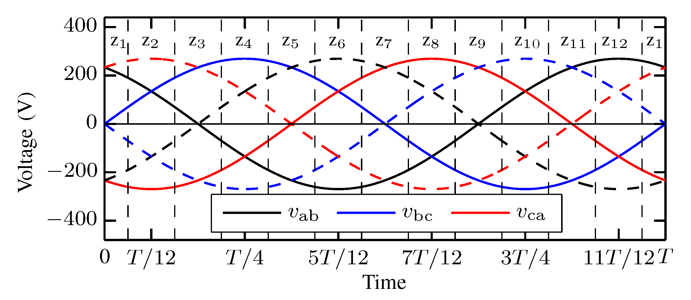
Figure 3.
Current space vectors of the shunt converter with 12 zones (dashed lines). (a) All vectors and zones. (b) Vectors that can be applied in zone .
Figure 3.
Current space vectors of the shunt converter with 12 zones (dashed lines). (a) All vectors and zones. (b) Vectors that can be applied in zone .
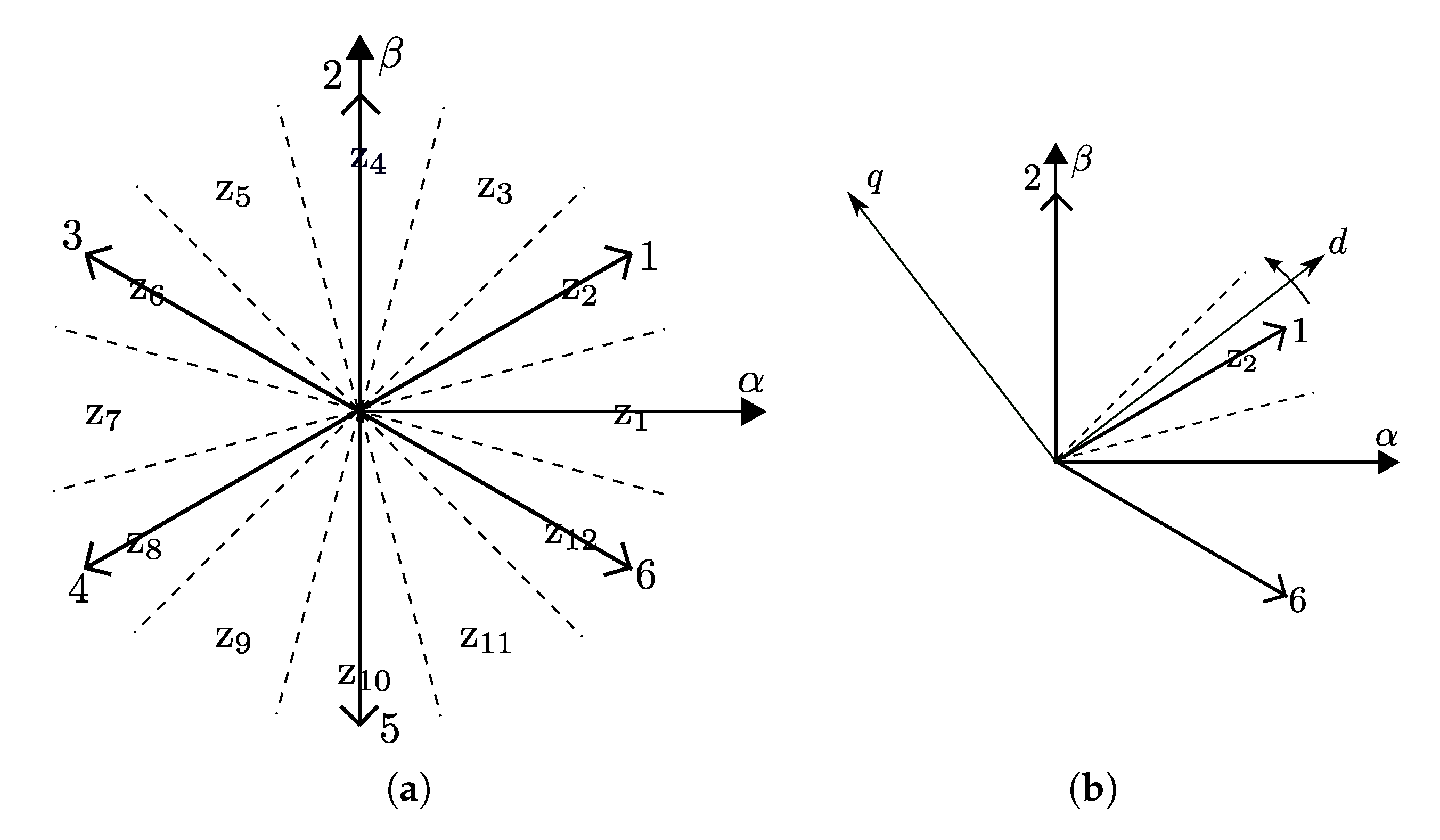
Figure 4.
Block diagram of the PV array current closed-loop control.
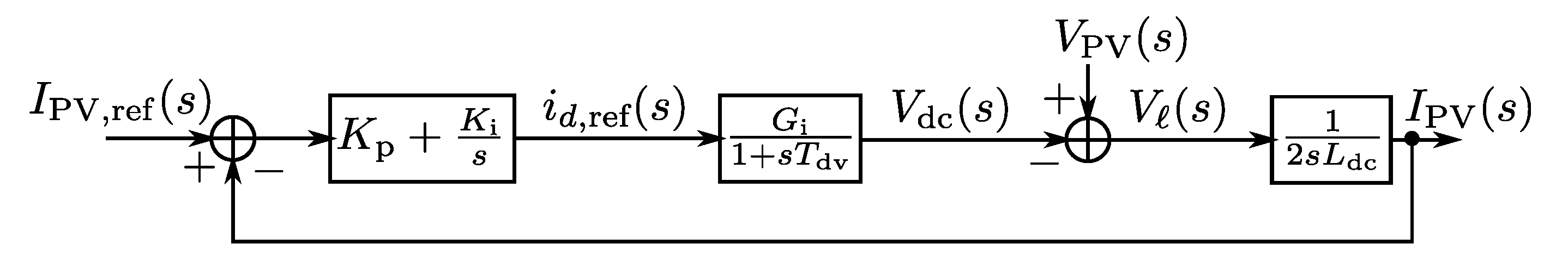
Figure 5.
Voltage space vectors of the series converter (for non-zero ‘dc link’ voltage) in the frame with the corresponding sliding variable values they are used for.
Figure 5.
Voltage space vectors of the series converter (for non-zero ‘dc link’ voltage) in the frame with the corresponding sliding variable values they are used for.
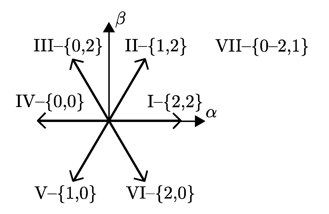
Figure 6.
Experimental setup: (1) shunt converter or 3×2 Matrix Converter (MC), (2) series converter or Voltage-Source Converter (VSC), (3) series transformer, (4) series filter capacitors, (5) series filter inductors, (6) shunt filter capacitors, (7) shunt filter inductors, (8) load resistor, (9) non-linear load diode full-bridge rectifier, (a) three-phase LV grid, (b) PV array emulator link, (c) dSPACE interface, (d) measurement board, (e) FPGA, (f) ‘dc link’, (g) isolation transformer.
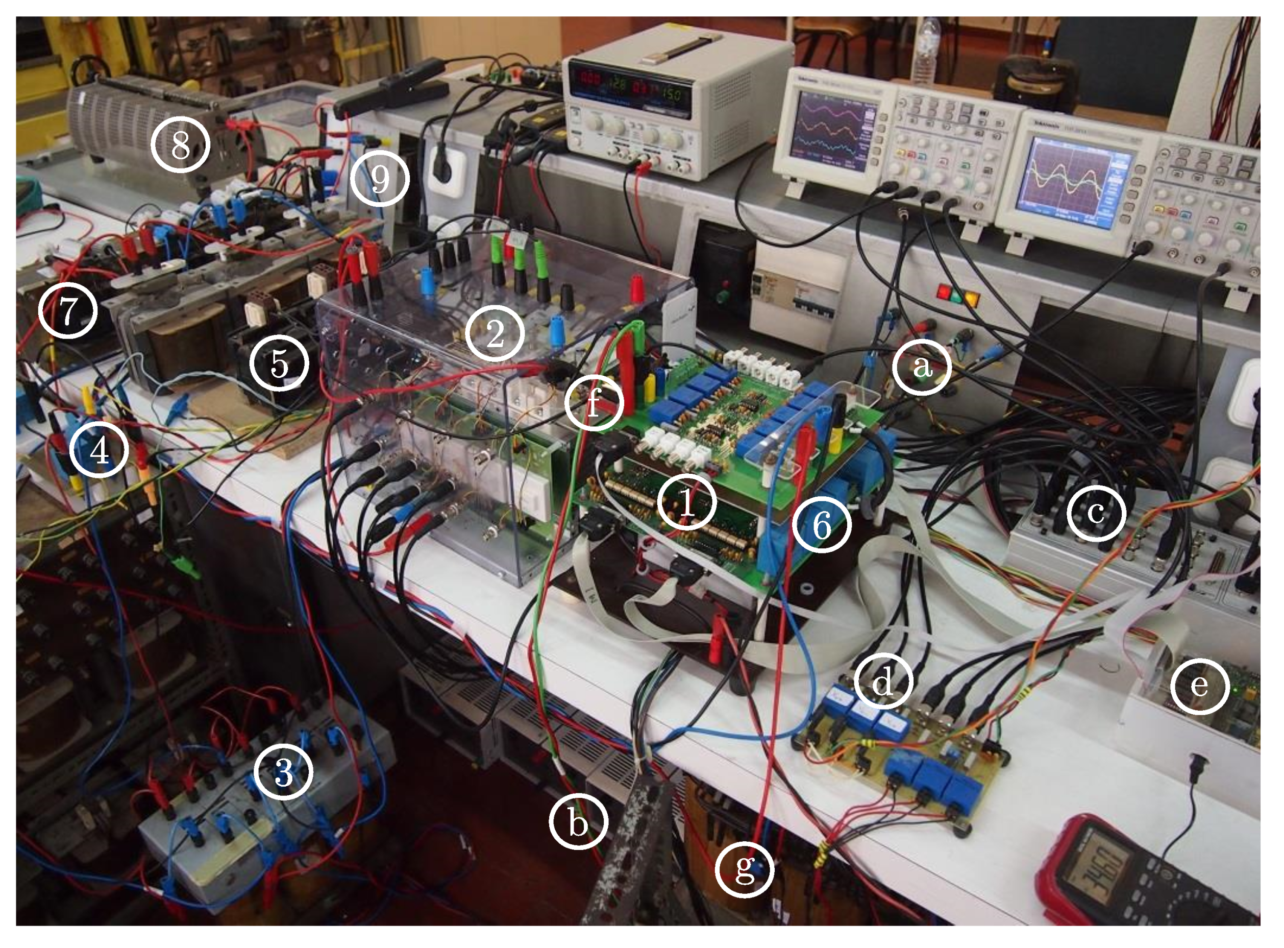
Figure 7.
Transitions between successive shunt converter vectors in a voltage zone. (a) Example for zone . (b) Example for zone .
Figure 7.
Transitions between successive shunt converter vectors in a voltage zone. (a) Example for zone . (b) Example for zone .

Figure 8.
Simulation and experimental results in no-load conditions. (a,d) ‘dc link’ voltage [100 /div], PV array current and shunt converter dc current [5 /div]. (b,e) Grid line-to-ground voltage [60 /div] and current [5 /div]. (c,f) Irradiance steps up and down between and : PV array current [2 /div] and grid currents [3 /div].

Figure 9.
Simulation and experimental results with a 250 non-linear load. (a,b) Grid line current , shunt converter ac line current and load line current [5 /div]. (c) Experimental grid line-to-ground voltage [60 /div] and line current [5 /div].
Figure 9.
Simulation and experimental results with a 250 non-linear load. (a,b) Grid line current , shunt converter ac line current and load line current [5 /div]. (c) Experimental grid line-to-ground voltage [60 /div] and line current [5 /div].

Figure 10.
Simulation results with a 2 resistive load and 250 non-linear load. (a) Grid line current , shunt converter ac line current and load line current [10 /div]. (b) Instantaneous active power flow from the grid , the shunt converter , the load and the PV array [400 /div]. (c) Reactive power flow from the grid , the shunt converter and the load [200 r/div].
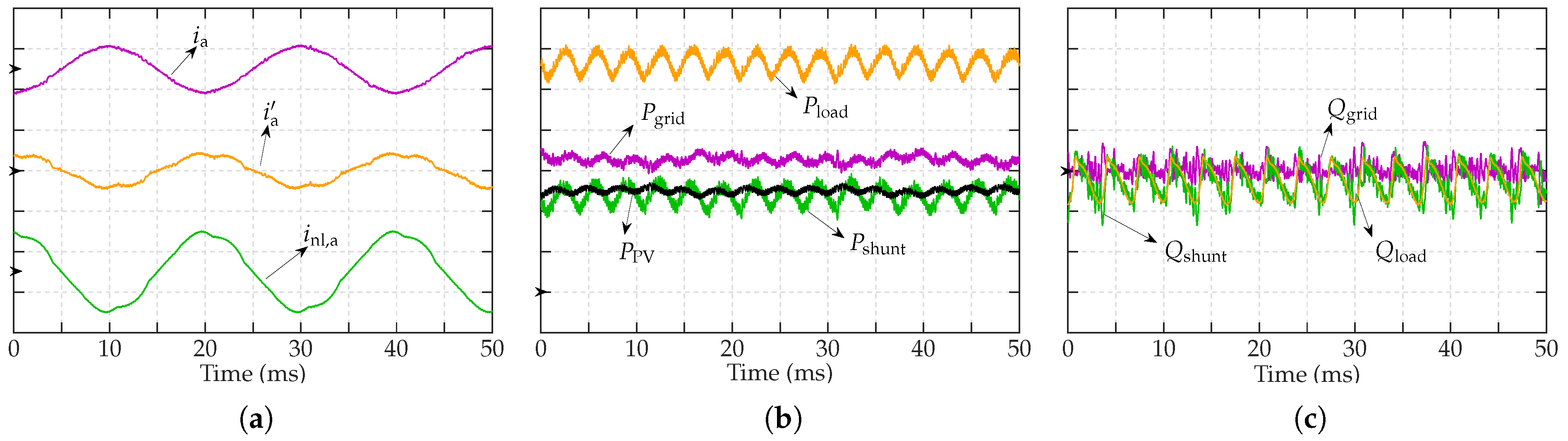
Figure 11.
Results with voltage sag and swell: grid line-to-ground voltage , series compensation line-to-line voltage and load line-to-ground voltage [125 /div] and grid line current [10 /div]. (a) Simulations: 10% sag from to with 10 degree phase-shift. (b) Simulations: 15% sag from to 0.15 and 10% swell from to . (c) Experiments with 15% sag. (d) Experiments with 10% swell.
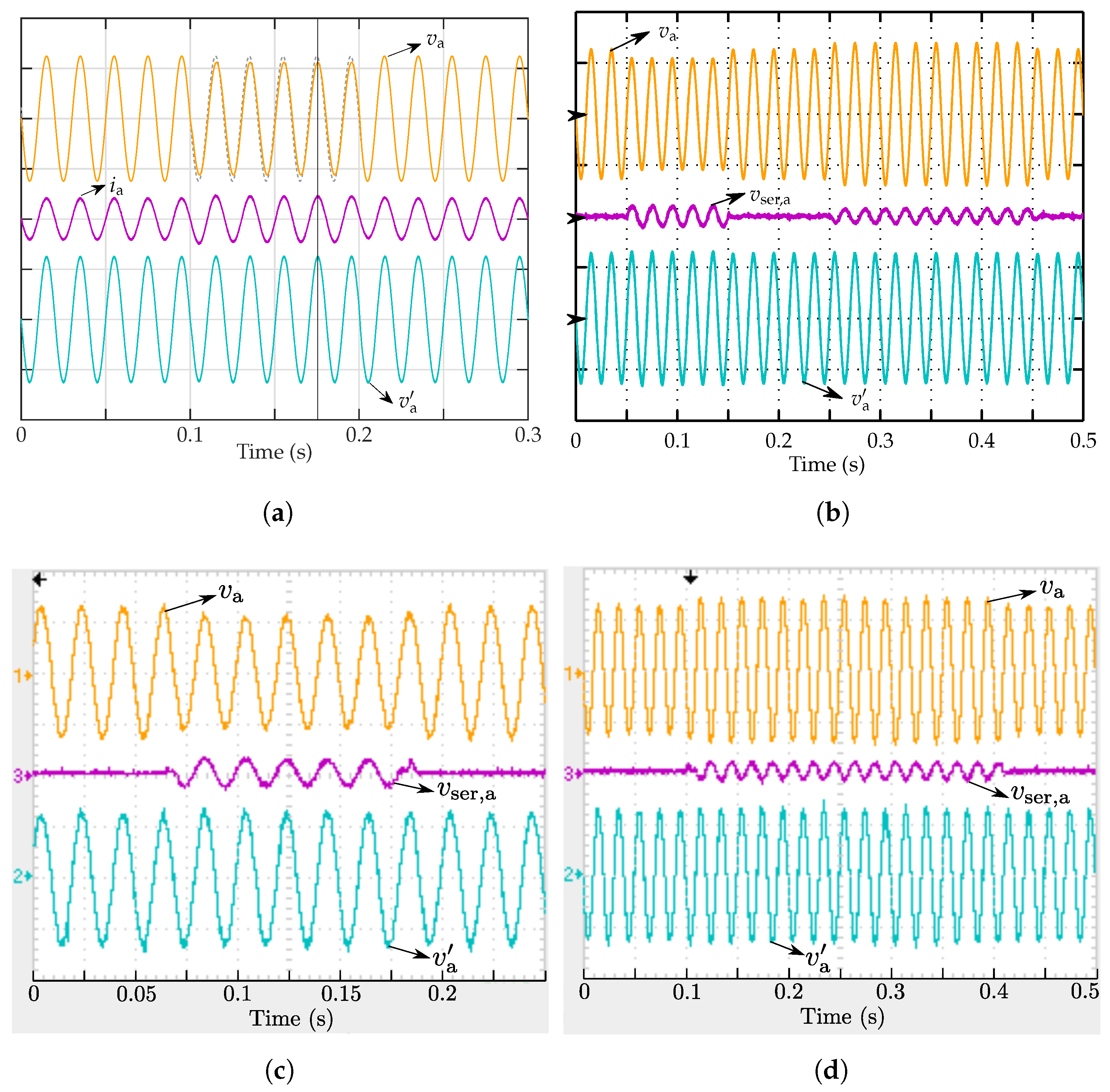
Figure 12.
Instantaneous power flow with 15% sag from to and 10% swell from to —simulation results.

Table 1.
Switching states of the shunt converter with the switches conducting on the upper (U) and lower (L) branch, with their effect on ‘dc link’ voltage and ac currents.
Table 1.
Switching states of the shunt converter with the switches conducting on the upper (U) and lower (L) branch, with their effect on ‘dc link’ voltage and ac currents.
| S | (U) | (L) | ||||||
|---|---|---|---|---|---|---|---|---|
| 1 | 0 | |||||||
| 2 | 0 | |||||||
| 3 | 0 | |||||||
| 4 | 0 | |||||||
| 5 | 0 | |||||||
| 6 | 0 | |||||||
| 7–9 | 0 | 0 | 0 | 0 | 0 | – |
Table 2.
Switching states of the series converter with the switches conducting on the first (1), second (2) and third (3) leg, with their effect on ‘dc link’ current and ac voltages.
Table 2.
Switching states of the series converter with the switches conducting on the first (1), second (2) and third (3) leg, with their effect on ‘dc link’ current and ac voltages.
| S | (1) | (2) | (3) | ||||||
|---|---|---|---|---|---|---|---|---|---|
| I | 0 | 0 | |||||||
| II | 0 | ||||||||
| III | 0 | ||||||||
| IV | 0 | ||||||||
| V | 0 | ||||||||
| VI | 0 | ||||||||
| VII(I) | 0 | 0 | 0 | 0 | 0 | – |
Table 3.
Non-zero allowed switching vectors of the shunt converter for each voltage zone considered.
Table 3.
Non-zero allowed switching vectors of the shunt converter for each voltage zone considered.
| Zone | ||||||||||||
|---|---|---|---|---|---|---|---|---|---|---|---|---|
| Vectors | 1,6 | 1,2,6 | 1,2 | 1,2,3 | 2,3 | 2,3,4 | 3,4 | 3,4,5 | 4,5 | 4,5,6 | 5,6 | 5,6,1 |
Table 4.
Switching vector selection for the shunt converter in function of the voltage zone and the sliding variables.
Table 4.
Switching vector selection for the shunt converter in function of the voltage zone and the sliding variables.
| Zone | |||||||||||||
|---|---|---|---|---|---|---|---|---|---|---|---|---|---|
| {,} | {0,0–2} | 7,8,9 | 7,8,9 | 7,8,9 | 7,8,9 | 7,8,9 | 7,8,9 | 7,8,9 | 7,8,9 | 7,8,9 | 7,8,9 | 7,8,9 | 7,8,9 |
| {2,0} | 6 | 6 | 1 | 1 | 2 | 2 | 3 | 3 | 4 | 4 | 5 | 5 | |
| {2,1} | 1 | 1 | 2 | 2 | 3 | 3 | 4 | 4 | 5 | 5 | 6 | 6 | |
| {2,2} | 1 | 2 | 2 | 3 | 3 | 4 | 4 | 5 | 5 | 6 | 6 | 1 | |
Table 5.
System parameter values.
| Symbol | Description | Value | Units |
|---|---|---|---|
| Sample time | 18 | ||
| Grid line-to-ground rms voltage | 110 | ||
| Grid frequency | 50 | ||
| n | Series transformer turns ratio | 3.31 | - |
| Shunt filter line-to-line capacitance | 6.6 | ||
| Shunt filter line inductance | 4 | ||
| Shunt filter damping resistance | 40 | ||
| Series filter line-to-line capacitance | 20 | ||
| Series filter line inductance | 6 |
Publisher’s Note: MDPI stays neutral with regard to jurisdictional claims in published maps and institutional affiliations. |
© 2020 by the authors. Licensee MDPI, Basel, Switzerland. This article is an open access article distributed under the terms and conditions of the Creative Commons Attribution (CC BY) license (http://creativecommons.org/licenses/by/4.0/).
Share and Cite
MDPI and ACS Style
Geury, T.; Pinto, S.F.; Gyselinck, J.; Wheeler, P. Indirect Matrix Converter-Based Grid-Tied Photovoltaics System for Smart Grids. Energies 2020, 13, 5405. https://doi.org/10.3390/en13205405
AMA Style
Geury T, Pinto SF, Gyselinck J, Wheeler P. Indirect Matrix Converter-Based Grid-Tied Photovoltaics System for Smart Grids. Energies. 2020; 13(20):5405. https://doi.org/10.3390/en13205405
Chicago/Turabian StyleGeury, Thomas, Sonia Ferreira Pinto, Johan Gyselinck, and Patrick Wheeler. 2020. "Indirect Matrix Converter-Based Grid-Tied Photovoltaics System for Smart Grids" Energies 13, no. 20: 5405. https://doi.org/10.3390/en13205405
Note that from the first issue of 2016, this journal uses article numbers instead of page numbers. See further details here.