Dual-Loop-Based Current Controller for Transformerless Grid-Tied Converters with Improved Disturbance Attenuation against Voltage Measurement Errors


School of Electrical and Information Engineering, Tianjin University, Tianjin 300072, China
*
Author to whom correspondence should be addressed.
Energies 2019, 12(5), 903; https://doi.org/10.3390/en12050903
Submission received: 29 January 2019
/
Revised: 22 February 2019
/
Accepted: 25 February 2019
/
Published: 8 March 2019
Abstract
:To eliminate current harmonics and to obtain enhanced dynamic behaviors, the voltage feedforward scheme is normally adopted in the control process of transformerless grid-tied converters. However, voltage measurement errors caused by parameter variation of sampling resistance and zero-voltage drift in analog devices will result in DC current injection and distorted grid currents in grid-tied systems. Conventional compensation strategies based on plug-in repetitive controllers and multiple resonant controllers are considered to be effective solutions to solve this problem. Even though undesired components in grid currents can be partially mitigated with these conventional compensation schemes adopted, degraded reference-tracking process with oscillations and slow dynamics are inevitably caused by the controller coupling. To obtain decoupling between reference tracking and disturbance rejection, this paper proposes a dual-loop controller to achieve current regulation and to suppress the disturbances caused by voltage measurement errors. With the proposed dual-loop controller adopted, DC current injection and distortion of grid currents can be effectively attenuated while excellent transient performance with negligible overshoot and fast step response can be simultaneously guaranteed. Frequency-domain analysis and experimental validations are both conducted to verify the effectiveness of the proposed strategy.
1. Introduction
Grid-tied converters are often used as the interface between distributed generation systems and the unity grid. Compared with conventional grid-tied converters equipped with transformers, transformerless grid-tied converters are directly connected to the grid through passive filters without using isolation transformers [1]. Due to the superiority of higher efficiency and smaller size, this topology has gained increasing attention [2,3,4]. However, because of the absence of galvanic isolation, it is more demanding for the transformerless grid-tied converters to meet the strict grid codes, such as the total harmonic distortion (THD) [5], the maximum DC current injection [6], and the maximum response time for voltage dynamics [7].
Typically, to eliminate current harmonics [8] and to obtain enhanced dynamic behaviors, the voltage feedforward scheme is normally adopted in the current control loop of grid-tied converters [9,10]. A large amount of research has been previously conducted in this area to obtain improved performance [11,12,13]. However, due to the parameter deviation in the conditioning circuit and the non-idealities in the low-pass filter, voltage measurement errors normally exist, which mainly includes offset errors, scaling errors, and the phase shift. Despite the theoretical efficiency of the voltage feedforward (VFF) scheme regarding the dynamic enhancement and the harmonic rejection, its performance can be greatly degraded in practical applications due to voltage measurement errors. This phenomenon has been widely investigated in previous research [14,15,16,17,18]. As analyzed in [14], offset errors in the VFF scheme generate undesired DC components in the grid currents. The fundamental frequency power fluctuations are thus introduced to the DC side, and the DC voltage ripples together with second-order harmonics in the grid currents are simultaneously produced accordingly [15,16]. In [17,18], it is concluded that offset and scaling errors will simultaneously generate DC currents and harmonic components. In addition, the phase shift in the VFF scheme mainly enlarges the amplitude of the periodic disturbances without changing their frequencies [13].
According to the standard IEEE 929-2000, the DC current injected by transformerless grid-tied converters should be less than 0.5% of the rated current. Moreover, the injected grid current should be balanced and sinusoidal with the THD less than 5%, as specified in the standard IEEE 1517-2003. In order to obtain satisfactory grid currents under voltage measurement errors, additional modifications need to be introduced to the VFF scheme of grid-tied converters. In [13], a simplified repetitive predictor is designed, where the phase-shift compensation is taken into account. In this manner, the accuracy of the VFF scheme is improved, and the distortion of the grid currents can be then suppressed. However, this method can only deal with the phase-shift problem, while the DC current injection and the current harmonics caused by offset and scaling errors cannot be effectively mitigated. Differently, with the influence of voltage measurement errors considered as periodic disturbances in the synchronous reference frame, the plug-in repetitive controller (RC) and multiple resonant controllers (MRSCs) are considered as effective strategies, which can be embedded in the current control loop of transformerless grid-tied converters to achieve periodic-disturbance rejection [17,18,19].
By combining the time delay and the positive feedback loop, the RC can simultaneously include the internal models of harmonic components. According to the internal model principle, it enables the RC to regulate the all the harmonic components. On the other hand, as a series of time delay is always embedded in the controller, the convergence rate of the plug-in RC is relatively slow in practical applications. To solve this problem, MRSCs can be applied instead of the plug-in RC. In MRSCs, to selectively embed internal models in the controller, multiple resonant controllers corresponding to different harmonic components are normally connected in parallel. Even though improved dynamic responses can be obtained, the adoption of multiple resonant controller results in tuning difficulties and heavy computational burden, especially when the number of embedded resonant controllers increases [20]. More importantly, these previously proposed compensation schemes, such as plug-in RCs and MRSC, are implemented via series or parallel connections with the main controller in the current loop. These control strategies belong to the single-degree-of-freedom control structure, where the reference-tracking performance of the current control will be inevitably degraded by the embedding of RC or MRSCs, resulting in coupling effects between reference tracking and periodic-disturbance rejection.
Taking both reference tracking performance and disturbance rejection aspects into account, several controllers have been proposed to deal with changes in the power system, such as load variation, generation changes, and faults. For example, in [21], to enhance the transient process under unbalanced conditions, a quadratic prediction algorithm has been proposed in combination with the strategy called set point automatic adjustment with correction enabled. In addition, the improvement introduced by the corresponding quadratic prediction algorithm enables the reduction of undesired peaks in transient processes. In [22], a generic nonlinear multi-input single-output self-tuning controller is employed to damp the oscillations under various post-disturbance operating conditions, and the proposed method has been proved to be superior to the conventional model-based controller. Additionally, considering parameter uncertainties in systems, reachability analysis is used in [23] for controller tuning, which can ensure stable operation against parameter uncertainties in power systems.
Aiming at realizing decoupling between reference tracking and disturbance mitigation, this paper proposes a dual-loop current controller, in which the reference-tracking performance is only determined by the primary tracking controller, and disturbance mitigation is realized by embedding an additional disturbance-rejection loop. Specifically, the internal-model-based primary tracking controller is designed following the state-space methods, which benefits the design of current regulation performance in the stationary coordinates. In addition, the embedded disturbance-rejection loop is designed with strong attention for DC and harmonic disturbances introduced by voltage measurement errors. To evaluate the performance of the proposed dual-loop controller, simulations and experiments are applied under both normal operation condition and unbalanced network condition.
This paper is organized as following. In Section 2, the impacts of voltage measurement errors on system operating characteristics are analyzed. The proposed dual-loop controller is clarified in Section 3, and the frequency-domain comparisons are presented in Section 4. The effectiveness of the proposed dual-loop controller is experimentally verified in Section 5. In addition, the conclusions are finally drawn in Section 6.
2. Impacts of Voltage Measurement Errors on System Operating Characteristics
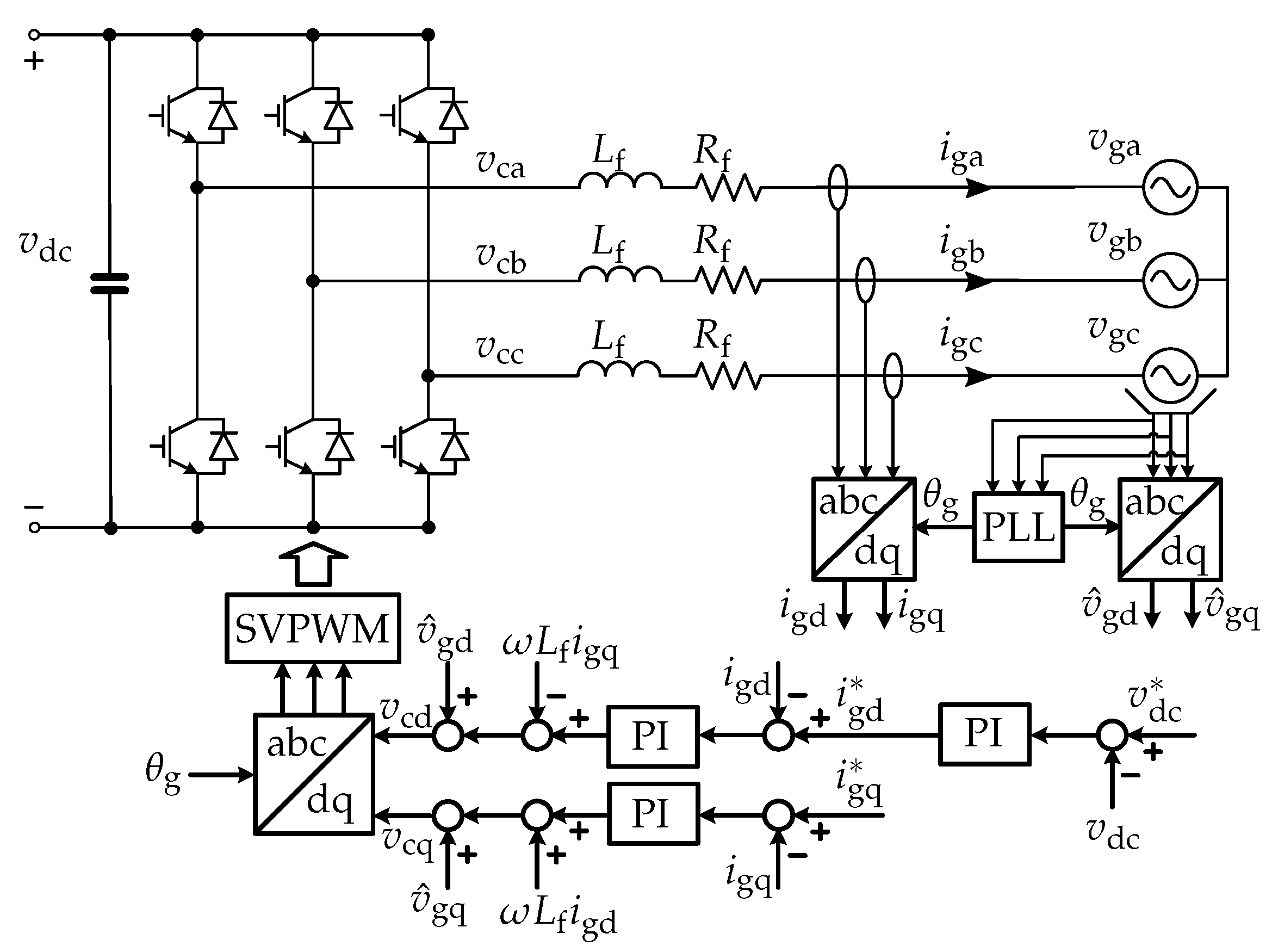
The classical control scheme of the transformerless grid-tied converter with a VFF scheme is shown in Figure 1, where the converter is connected to the utility grid via the inductors . The equivalent resistor is represented by . , , and stand for the converter output voltages. , , and represent the grid currents. , , and are the grid voltages. and denote the fundamental angular frequency and the phase information of the grid, respectively. The linear proportional integral (PI) controllers are normally applied together with feedforward decoupling terms in the coordinates to construct the inner current loop. In addition, the measured grid voltages are normally included in feedforward terms as well. In this manner, the grid currents can be expressed in the coordinates as
where and denote the proportional gain and the integral gain of PI controllers, respectively. and are current references, and and are measured grid currents in the coordinates. and are actual grid voltages, and and are measured grid voltages in the coordinates.
As can be seen in Equation (1), the accuracy of the grid-voltage measurement has straightforward impacts on grid currents. In the case of accurate compensation (i.e., , ), the fundamental component together with harmonic components of grid voltages can be simultaneously compensated. However, due to the parameter deviation of the sampling resistance, the zero-voltage drift of analog devices, and the phase shift introduced by low-pass filters, offset errors, scaling errors, and the phase shift may exist in the voltage measurement. As analyzed in [18], in the coordinates, offset errors generate disturbances at . Both scaling errors and grid-voltage harmonics at will result in disturbances at DC and . It is worth noting that the phase shift mainly enlarges the amplitude of the periodic disturbances without changing the frequency [13]. In this manner, disturbances caused by voltage measurement errors can be written as
where and stand for DC disturbances in the coordinates. , , , and represent AC disturbances in the coordinates. Due to the limitation of linear PI controller regarding AC signal tracking, the periodic disturbances cannot be completely eliminated by the control structure shown in Figure 1. Subsequently, these disturbances will generate undesired AC ripples at and in and .
By applying coordinate transformation, the disturbances formulated in the coordinates can be transformed into the coordinates as
where and are actual grid voltages, and and are measured grid voltages in the coordinates. and stand for dc disturbances in the coordinates. , , , and represent AC disturbances in the coordinates.
3. The Proposed Dual-Loop-Based Current Control Scheme
For better understanding, two typical compensation schemes are shown in Figure 2. In Figure 2a, the plug-in RC in the current control loop is used to attenuate disturbances generated by voltage measurement errors, and the conventional linear PI controllers are used as the main controller to regulate three-phase currents of fundamental frequency. In practical applications, the RC are normally realized by a serious of time delay. In this manner, the convergence rate of the disturbance mitigation will be inevitably slow when the RC is applied in the control loop. Moreover, since additional low-pass filters are normally embedded in the RC to ensure enough stability margin, the open-loop gains for disturbances will then be inevitably reduced, resulting in degraded disturbance-mitigation performance.
As an alternative, MRSCs can be implemented to eliminate disturbances introduced by voltage measurement errors, as depicted in Figure 2b. When the MRSCs are adopted, multiple resonant controllers are connected in parallel and embedded to the current control loop, with the aim of eliminating disturbances of different frequencies. Under this situation, the controller parameter tuning is thus a difficult task, and the parallel computational burden of the controller is heavy. Most importantly, in the control schemes using plug-in RC and MRSCs, the coupling between the main controller and the disturbance-mitigation controller always exists. As depicted in Figure 2a,b, the control signals for reference tracking and disturbances elimination are not generated independently. In this manner, both the main PI controller and the disturbance-mitigation controller will take actions on the reference-tracking error. As a result, the transient performance of the reference tracking will be distorted with oscillations and slow responses, especially under the situation of a reference step change. This phenomenon will be further demonstrated by the frequency-domain analysis and the experimental validations in following sections.
Aiming at realizing the decoupling between reference tracking and disturbance rejection, this paper proposes the dual-loop controller. The corresponding current control loop using the proposed controller are shown in Figure 3, where and represent the reference-tracking controller and the disturbance-mitigation controller, respectively. is the estimated model of the plant, is the discrete-time model of the inductor, and is the actual plant with one sample period delay. In the proposed dual-loop control structure, is designed for tracking, and the embedded path containing is implemented for disturbance mitigation.
3.1. Design of the Reference-Tracking Controller
In the dual-loop control structure shown in Figure 3, the controller is adopted as the reference-tracking controller. Specifically, the function of the reference-tracking controller is to regulate the grid currents of fundamental frequency in the coordinates. For clarity and better understanding, in the following contents, boldfaced letters are used to denote matrices or complex vectors, and complex vector quantities are expressed in the stationary coordinates (e.g., ). With the zero-order-hold (ZOH) characteristic of the pulse width modulation taken into account, the hold-equivalent discrete-time model can be expressed as
where stands for the converter output voltage vector. denotes the grid-voltage vector. System matrices and are given by
where is the sampling period.
Under synchronous sampling mode, one sampling period delay is introduced inherently in the digital control system. For the direct discrete-time design, the time delay is embedded by adding an additional state (i.e., ) in the hold-equivalent discrete-time model as
where is the output reference voltage vector. and are system matrices, and is the state matrix. It is worth noting that is excluded from Equation (6) since it will be handled by the grid-voltage feedforward terms and the disturbance-rejection controller later.
To design the , the internal model of the sinusoidal references is written as
where . and are two states of the internal model.
From Equations (6) and (7), the internal model of the sinusoidal references is embedded in the hold-equivalent discrete-time model by means of state augmentation. In addition, the augmented model is given by
where and are the system matrices after the augmentation, and is the matrix of the augmented states.
, , and are
The structure of the proposed resonant controller is shown in Figure 4. denotes the feedback gain for the grid current. is the feedback gain for the previous output voltage. and represent the feedback gains for the states and , respectively. In additional, is the reference-feedforward gain, and . It is worth noting that both and are used in the feedback control to achieve additional degree of freedom. Because the state corresponds to a single sampling period delay is included in the design as well, accurate pole locations can be realized for the system with time delay [24].
According to Figure 4, the control law can be written as
where . From Equations (8) and (10), the dynamic of the closed-loop system is given as
where .
For the closed-loop system, there are four closed-loop poles to be placed. These poles are introduced by the time delay, the inductor, and the internal model, respectively. The pole introduced by the time delay is in the optimal point and will not be moved. The pole originating from the inductor can be cancelled by the reference-feedforward path. To obtain enhanced tracking performance of sinusoidal references, two dominant poles can be then selected as
where is related to the desired bandwidth, and the damping ratio is normally set to a proper value (i.e., 0.7∼1). The direct pole placement mentioned above can be easily accomplished in the MATLAB [24], where and can be simultaneously obtained.
3.2. Design of Disturbance-Mitigation Controller
In the proposed dual-loop control structure shown in Figure 3, the disturbance-mitigation controller is used to suppress DC disturbances and AC disturbances at disturbances caused by voltage measurement errors.
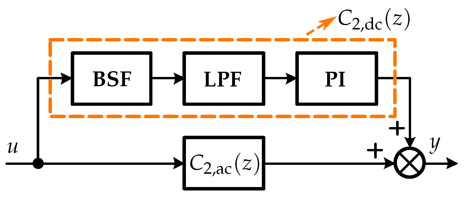
The scheme of the proposed is shown in Figure 5. In this figure, and are designed to suppress DC and AC disturbances, respectively. The controller is expressed as
where is the control gain.
The frequency response of controller is shown in Figure 6. Because the internal model of the fundamental-frequency signals is embedded in the reference-tracking controller , it mainly produces high gain for grid currents of fundamental frequency. In this manner, the controller should be inactive to fundamental-frequency components to avoid coupling between and the additional path shown in Figure 3. Correspondingly, the magnitude of the controller is designed to be low at the fundamental frequency, as shown in Figure 6. Moreover, to effectively attenuate AC disturbances at , are designed with high gains at the selected frequencies (i.e., 3rd, 5th, 7th, 9th, 11th harmonics). The decoupling between reference tracking and disturbance mitigation can be ensured, and the satisfactory disturbance-mitigation performance can be simultaneously obtained. It should be noted that only one single control gain is required in the controller , and the parameter tuning of is thus simple.
The controller can only eliminate AC disturbances while DC disturbances generated by the voltage measurement errors cannot be effectively regulated. To effectively eliminate DC disturbances, an additional controller is connected in parallel, as shown in Figure 5. Specifically, the controller consists of a second-order bandpass filter (BSF), a first-order low-pass filter (LPF), and a PI controller. The PI controller in is used as the main controller to mitigate DC disturbances. Because PI controller can produce gain for fundamental-frequency components as well, the second-order BSF is adopted here to filter out the signals at the fundamental frequency, and the first-order LPF is used to filter out high-frequency signals and improve the stability region. The transfer function of the second-order BSF is written as
where is the center frequency, and is the control gain for the adjustment of the stopband.
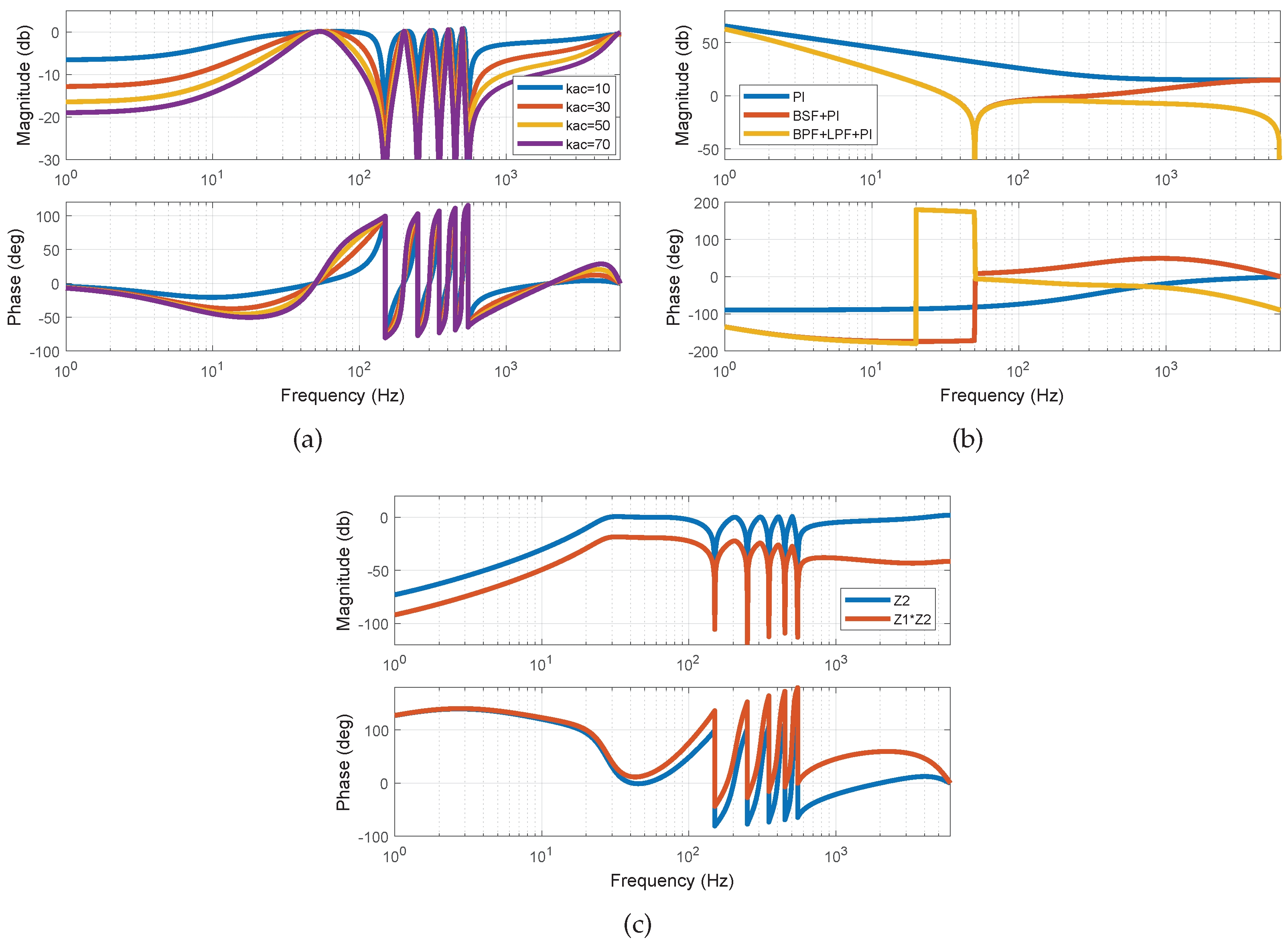
The frequency response of the bandpass filter is plotted in Figure 7, where the center frequency is set to the fundamental frequency. With the growth of , the stopband of BSF becomes wider, and the attenuation of fundamental-frequency signals can be thus improved.
With the Tustin with pre-warping discretization method applied, the transfer function (14) is rewritten in the z-domain as
where the coefficients are
The transfer function of the first-order LPF is expressed as
where is used to adjust the cutoff frequency () of the LPF.
The expression of the linear PI controller is
where is the proportional gain, and is the integral gain.
3.3. Parameter Tuning
Using the proposed dual-loop controller, the reference-tracking performance is only determined by , and the dynamic of tracking can be properly designed by adjusting the damping ratio and the bandwidth of dominant closed-loop poles in Equation (12). In this paper, the damping ratio is set to 0.7 to prevent large overshoots, and the bandwidth is set to 1000 rad/s to realize a fast step reference response. For disturbances attenuation, as derived from Figure 3, the transfer function from the disturbance caused by voltage measurement errors to the grid current can be written as
where and are two frequency-selective filters. From Equation (19), it can be concluded that the disturbance-rejection performance of the current control loop can be designed by properly choosing and . Since is already determined by , the disturbance-mitigation performance of the current control loop is then only determined by . In , the actual plant model cannot be changed, thus need to be tuned to achieve desired disturbance attenuation.
In the proposed disturbance-mitigation controller , two channels (i.e., and ) are responsible for the regulation of signals at different frequencies. As indicated in Figure 5, is used to eliminated periodic disturbances while is responsible for the mitigation of DC disturbances. In this way, the control gains in and can be selected independently. Assuming only is applied, the frequency response of is presented in Figure 8a. As it can be seen, with the growth of , the magnitude of at harmonic frequencies are lower, and the disturbance-rejection ability of the system is thus improved. To realize a satisfactory regulation performance against harmonics, is set to 30 in this paper. Regarding , , and , there are four parameters (i.e., , , , and ) to be determined. As indicated in Figure 8b, and are set to 15 and 1 respectively to ensure enough open-loop gain for the DC signals, and in the BSF is then set to 50 for a wide enough stopband for components of fundamental frequency. Finally, is chosen to adjust the cutoff frequency of the LPF, and the high-frequency signals are then filtered effectively. With all the parameters in determined, the frequency response of is presented in Figure 8c. To evaluate the disturbance-attenuation performance of the proposed dual-loop controller, the frequency response of is plotted in Figure 8c as well. As is clearly visible, DC and periodic disturbances caused by voltage measurement errors can be effectively attenuated.
4. Frequency-Domain Comparisons between the Proposed Dual-Loop Strategy and Conventional Compensation Schemes
In the conventional compensation scheme shown in Figure 2a, the s-domain transfer function of the current controller containing the plug-in RC can be expressed as
where and represent the PI controller and the RC, respectively. , , and stand for the proportional, the integral, and the RC gains, respectively. stand for the fundamental period. is the LPF and is the phase-lead compensator embedded in the RC. The transfer function from the reference current to the output current can be expressed as
where represents the plant model in the s-domain. It should be noted that both the main controller and the disturbance-mitigation controller exist in the transfer function (21), which indicates that the disturbance-mitigation controller will inevitably affect the process of reference tracking. This coupling will significantly influence reference tracking and result in distorted transient performance, especially under a step reference change. This phenomenon will be further verified by experimental results in following sections.
When MRSCs are applied as disturbance-mitigation controllers instead of the plug-in RC, as shown in Figure 2b, the transfer function of the current controller can be written as
where and stand for the PI controller and MRSCs, respectively. and are the proportional and integral gains of PI controllers. and are the proportional and resonant gains of resonant controllers, respectively. Under this situation, the transfer function of reference tracking can be written as
Similar to Equation (21), the disturbance-mitigation controller appears in the transfer function of reference tracking as well. This implies that the coupling still exists in the case of applying MRSCs, which may inevitably affect the tracking processes. With aim of solving the coupling problem existing in conventional compensation schemes, this paper proposed a dual-loop controller, as shown in Figure 3. Under the assumption that the estimated plant model can approximately represent the actual plant (i.e., ), the transfer function of reference tracking can be formulated as
From Equation (24), it can be seen that the disturbance-mitigation controller is successfully removed from the reference-tracking transfer faction, and the tracking performance is only determined by the controller . Therefore, different from traditional control schemes presented in Figure 2a,b, the coupling between the reference tracking and disturbance mitigation can be avoided, and desired tracking performance without oscillations can be achieved.
To illustrate the differences between the proposed dual-loop controller and conventional compensation schemes using the plug-in RC and MRSCs, the frequency-domain comparison is also conducted. The frequency response of reference-tracking transfer functions (i.e., Equations (21), (23), and (24)) is shown in Figure 9a,b. As it can be observed, when the conventional compensation schemes, and , are adopted, signals around the resonant frequencies are amplified or micrified.
When the plug-in RC is adopted for disturbance attenuation, a series of peaks are simultaneously generated at various frequencies, as indicated in Figure 9. To illustrate these undesired fluctuations, the LPF and the phase-lead compensator are excluded from the plug-in RC, and the transfer function of the ideal RC can be expanded as
Equation (25) indicates that the RC can be equivalently seen as a parallel combination of a proportional term, an integral term, and all resonant terms of different frequencies. The corresponding frequency response of the ideal RC is presented in Figure 10, and it can be observed that peaks are simultaneously introduced by resonant terms in Equation (25) without taking the harmonic distribution into account. Due to this feature of the RC, peaks at various frequencies occur in the Figure 9a.
It is worth noting that due to the undesired fluctuations in the frequency response of reference-tracking transfer function, the transient response will be inevitably distorted when the reference is step changed. Differently, when the dual-loop controller is used, the corresponding frequency response is smooth as desired. This is because the disturbance-mitigation controller is excluded from the reference-tracking transfer function. In this manner, decoupling between disturbance mitigation and reference tracking is achieved, and satisfactory transient performance can be obtained in the reference-tracking process. Corresponding experimental validations will be presented in the following sections.
5. Simulation and Experimental Results
To verify the effectiveness of the proposed control strategy, experimental verifications are performed on a 7.5-kVA transformerless grid-tied system. In the experiment, the fundamental frequency of the grid is 50 Hz, and the switching frequency of the grid-tied converter is 6 kHz. The equivalent resistor and the equivalent inductor are 0.3 and 6.6 mH. The damping ratio and the bandwidth of dominant poles in Equation (12) are set to 0.7 and 1000 rad/s, respectively. In addition, the control gain of is set to . The proportional and the integral gains of are set to and , respectively. The center frequency of is set to rad/s, and the control gain is . The cutoff frequency of is set to Hz. In the experiment, the control algorithm is implemented using the DSP TMS320F28379D, and the waveforms of grid currents are recorded by the DLM2040 oscilloscope. Voltage measurement errors are given in Table 1.
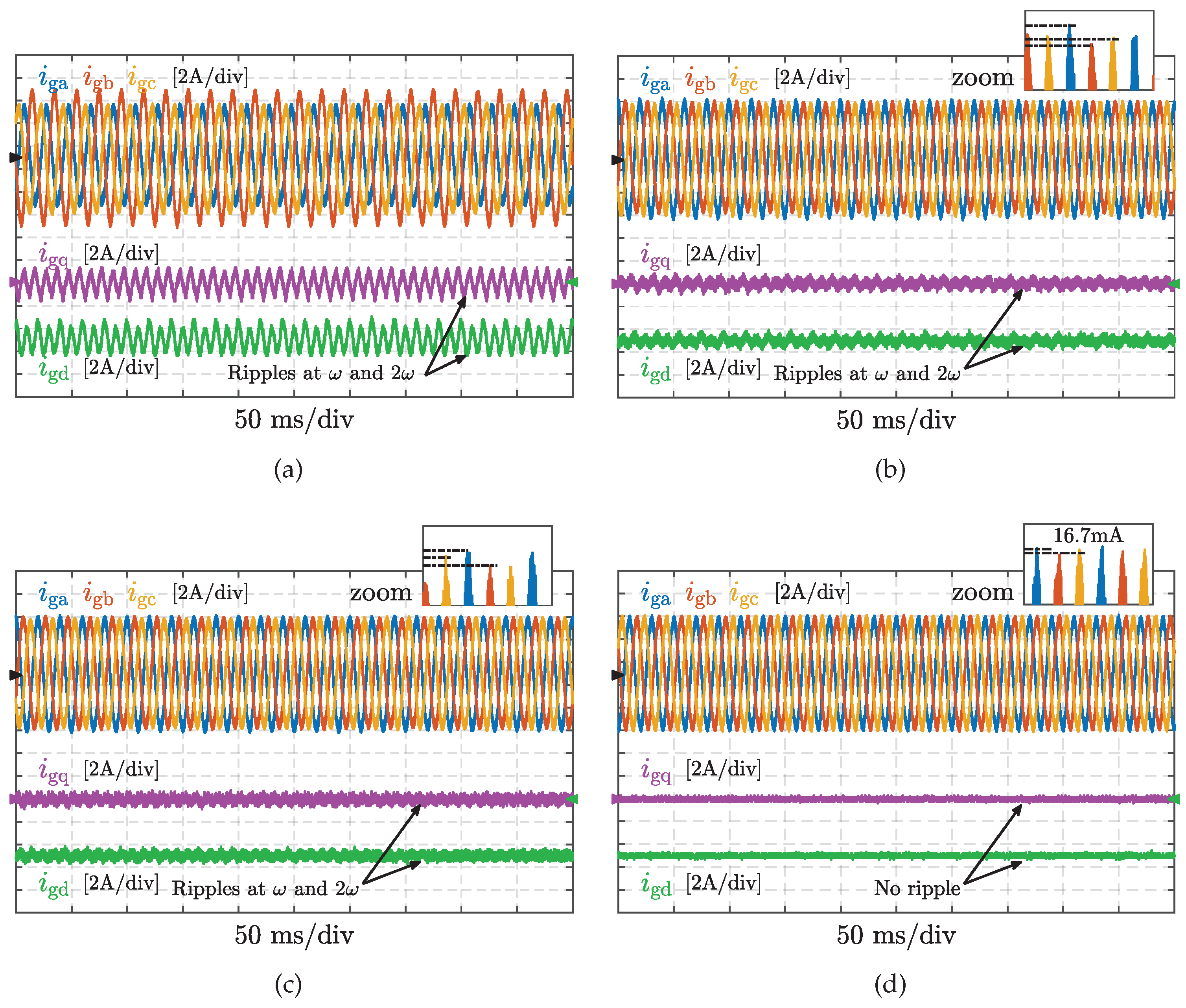
Figure 11 shows the waveforms of grid currents under voltage measurement errors. In the experiment, the conventional control structure shown in Figure 1 is firstly applied, where no additional compensation scheme is adopted for the current regulation. The corresponding experimental waveforms are shown in Figure 11a, and it can be observed that AC ripples at and occur in the currents and simultaneously. It is worth noting that the origination of these undesired AC components in and is the disturbance introduced by voltage measurement errors (i.e., , , , and in Equation (2)). When the conventional compensation scheme based on MRSCs is implemented in the current control loop, these undesired AC ripples are partially attenuated, as shown in Figure 11b. However, due to the limited control gain together with the shifted resonant peaks caused by discretization errors, these ripples in and are not effectively mitigated, and the three-phase grid currents are unbalanced with DC components. Similarly, when the RC is adopted as the disturbance-mitigation controller, disturbances are not completely eliminated, and undesired components still exist in grid currents, as shown in Figure 11c. As a comparison, once the proposed dual-loop controller is applied, the currents and are smooth enough, and the grid currents are sinusoidal without unbalances, as indicated in Figure 11d. In particular, the DC component in grid currents is regulated to 16.7 mA which is below the limitation listed in the IEEE 929-2000.
Additionally, as analyzed in the previous sections, the coupling issue in the conventional compensation schemes will lead to distorted transient performance during the reference tracking process. To demonstrate this phenomenon, a reference step change is generated under the same experimental conditions. As shown in Figure 12a, in case that PI controllers are used without additional compensation schemes, steady-state -axis currents are same as the waveforms presented in Figure 11a, and no obvious distortions can be observed in the transient processes. Nevertheless, when the conventional compensation scheme based on MRSCs is applied, dynamics of the reference tracking are slowed down with oscillations, as shown in Figure 12b. Instead of MRSCs, when the plug-in RC is adopted for the disturbance mitigation, experimental results are presented in Figure 12c. It can be seen that the distorted dynamics are introduced in the reference-tracking process as well. Because frequency responses of the reference tracking are similar under these two conventional control schemes, the distortion are alike in both Figure 12b,c. In contrast, Figure 12d shows the experimental results with the proposed dual-loop controller. Obviously, the disturbances caused by voltage measurement errors are substantially attenuated with satisfactory reference-tracking performance well preserved, and the transient process is fast without any oscillation.
To evaluate the effectiveness of the proposed method under unbalanced network condition, simulations are used in this case study. As indicated in Figure 13a, when the conventional lineal controller is applied in the current control loop of grid-connected transformerless converters, DC and negative-sequence components are inevitably generated in three-phase grid currents. Correspondingly, periodic ripples at and occur in the coordinates. It is worth noting that both positive-sequence and negative-sequence controllers can be used for the current regulation under unbalanced network condition. In this manner, ripples at can be then suppressed in the coordinates, while ripples at will still occur in d- and q-axis currents. However, when the proposed dual-loop controller is applied under the same condition, disturbances generated by voltage measurement errors are effectively eliminated. Three-phase currents are regulated to follow the references accurately, and no obvious ripples can be observed in d- and q-axis currents, as shown in Figure 13b.
To validate the harmonic-elimination performance under different strategies, experiments are performed under distorted voltages together with voltage measurement errors, and the corresponding results are shown in Figure 14. It can be observed that the grid currents contain plenty of harmonic components when the traditional controller is adopted without additional compensation scheme. In addition, these harmonic currents can be effectively eliminated when the MRSCs, the RC, and the dual-loop controller are implemented. To further evaluate the performance of these control methods in terms of THD, the corresponding harmonic distributions of the grid currents are plotted in Figure 15.
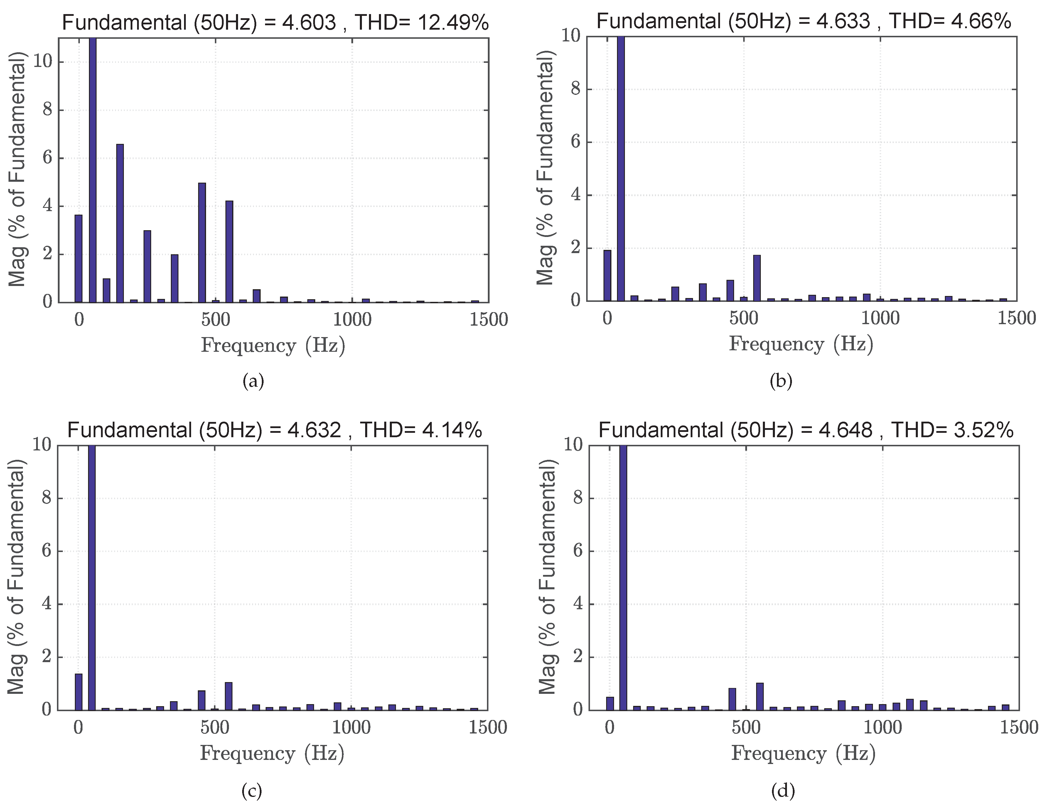
As shown in Figure 15a, without disturbance-mitigation controllers applied, the THD of the experimental waveforms is 12.49%. In case that the MRSCs are applied for the disturbance attenuation under the same condition, the THD of the grid currents reduces to 4.66%, as demonstrated by Figure 15b. Besides, when the plug-in RC is performed to regulate the harmonic currents, the corresponding harmonic distribution is presented in Figure 15c, in which the THD is around 4.14%. Even though the THD is already below the 5% limitation demanded by the standard IEEE 1517-2003, it can further reduce to 3.52% when the proposed dual-loop controller is adopted, as shown in Figure 15d.
6. Conclusions
In practical applications, nonideal factors in sampling channels will lead to measurement errors, and the resulted voltage measurement errors will cause undesired disturbances in the current control loop of transformerless grid-tied converters. If no compensation strategy is applied to attenuate these disturbances, serious DC current injection together with grid current distortion may occur in the transformerless grid-tied systems. To deal with this problem, the existing solution is to apply conventional compensation schemes based on plug-in RC and MRSCs. However, due to the coupling between reference tracking and disturbance rejection in these compensation schemes, degraded dynamic behaviors with oscillations can be observed under step reference change. To achieve decoupling between reference tracking and disturbance rejection, a dual-loop controller is proposed in this paper, in which reference tracking is only determined by the tracking controller and disturbance rejection is realized by an embedded attenuation loop. It is demonstrated that compared with the conventional compensation strategies, DC current injection and grid current distortion caused by voltage measurement errors are effectively mitigated, while satisfactory step response without oscillations can be simultaneously guaranteed. The effectiveness of the proposed controller is validated by simulation and experimental studies under both normal operation condition and unbalanced network condition.
Author Contributions
Z.S. and Y.Y. put forward the idea and designed the simulation and the experiments; Y.Y. performed the simulation and the experiments; all authors analyzed the results; all authors contributed to the writing of the paper; all authors reviewed and edited the manuscript.
Funding
This research was funded by The National Natural Science Foundation of China (Grant No. 51877150 & 51477113).
Conflicts of Interest
The authors declare no conflict of interest.
References
- Kjaer, S.B.; Pedersen, J.K.; Blaabjerg, F. A review of single-phase grid-connected inverters for photovoltaic modules. IEEE Trans. Ind. Appl. 2005, 41, 1292–1306. [Google Scholar] [CrossRef]
- Gonzalez, R.; Gubia, E.; Lopez, J.; Marroyo, L. Transformerless Single-Phase Multilevel-Based Photovoltaic Inverter. IEEE Trans. Ind. Electron. 2008, 55, 2694–2702. [Google Scholar] [CrossRef]
- Gu, B.; Dominic, J.; Lai, J.S.; Chen, C.L.; Labella, T.; Chen, B. High Reliability and Efficiency Single-Phase Transformerless Inverter for Grid-Connected Photovoltaic Systems. IEEE Trans. Power Electron. 2013, 28, 2235–2245. [Google Scholar] [CrossRef]
- Kerekes, T.; Teodorescu, R.; Rodriguez, P.; Vazquez, G.; Aldabas, E. A New High-Efficiency Single-Phase Transformerless PV Inverter Topology. IEEE Trans. Ind. Electron. 2011, 58, 184–191. [Google Scholar] [CrossRef] [Green Version]
- IEEE Standard 1547-2003. IEEE Standard for Interconnecting Distributed Resources with Electric Power Systems; IEEE: Piscataway, NJ, USA, 2003. [Google Scholar]
- IEEE Standard 929-2000. IEEE Recommended Practice for Utility Interface of Photovoltaic (PV) Systems; IEEE: Piscataway, NJ, USA, 2000. [Google Scholar]
- Bollen, M.H. Understanding Power Quality Problems: Voltage Sags and Interruptions; Wiley: New York, NY, USA, 2001. [Google Scholar]
- Abeyasekera, T.; Johnson, C.M.; Atkinson, D.J.; Armstrong, M. Suppression of line voltage related distortion in current controlled grid connected inverters. IEEE Trans. Power Electron. 2005, 20, 1393–1401. [Google Scholar] [CrossRef]
- Xu, J.M.; Xie, S.J.; Tang, T. Improved control strategy with grid-voltage feedforward for LCL-filter-based inverter connected to weak grid. IET Power Electron. 2014, 7, 2660–2671. [Google Scholar] [CrossRef]
- Zhao, M.; Yuan, X.; Hu, J.; Yan, Y. Voltage Dynamics of Current Control Time-Scale in a VSC-Connected Weak Grid. IEEE Trans. Power Syst. 2016, 31, 2925–2937. [Google Scholar] [CrossRef]
- Wang, X.; Ruan, X.; Liu, S.; Chi, K.T. Full Feedforward of Grid Voltage for Grid-Connected Inverter with LCL Filter to Suppress Current Distortion Due to Grid Voltage Harmonics. IEEE Trans. Power Electron. 2010, 25, 3119–3127. [Google Scholar] [CrossRef]
- Xue, M.; Zhang, Y.; Kang, Y.; Yi, Y.; Li, S.; Liu, F. Full Feedforward of Grid Voltage for Discrete State Feedback Controlled Grid-Connected Inverter With LCL Filter. IEEE Trans. Power Electron. 2012, 27, 4234–4247. [Google Scholar] [CrossRef]
- Yan, Q.; Wu, X.; Yuan, X.; Geng, Y. An Improved Grid-Voltage Feedforward Strategy for High-Power Three-Phase Grid-Connected Inverters Based on the Simplified Repetitive Predictor. IEEE Trans. Power Electron. 2016, 31, 3880–3897. [Google Scholar] [CrossRef]
- Trinh, Q.N.; Wang, P.; Choo, F.H. An Improved Control Strategy of Three-Phase PWM Rectifiers Under Input Voltage Distortions and DC-Offset Measurement Errors. IEEE J. Emerg. Sel. Top. Power Electron. 2017, 5, 1164–1176. [Google Scholar] [CrossRef]
- Shi, Y.J.; Liu, B.Y.; Duan, S.X. Eliminating DC Current Injection in Current-Transformer-Sensed STATCOMs. IEEE Trans. Power Electron. 2013, 28, 3760–3767. [Google Scholar] [CrossRef]
- Rioual, P.; Pouliquen, H.; Louis, J.P. Regulation of a PWM rectifier in the unbalanced network state using a generalized model. IEEE Trans. Power Electron. 1996, 11, 495–502. [Google Scholar] [CrossRef]
- Trinh, Q.N.; Choo, F.H.; Wang, P. Control Strategy to Eliminate Impact of Voltage Measurement Errors on Grid Current Performance of Three-Phase Grid-Connected Inverters. IEEE Trans. Ind. Electron. 2017, 64, 7508–7519. [Google Scholar] [CrossRef]
- Trinh, Q.N.; Wang, P.; Yi, T.; Choo, F.H. Mitigation of DC and Harmonic Currents Generated by Voltage Measurement Errors and Grid Voltage Distortions in Transformerless Grid-Connected Inverters. IEEE Trans. Energy Convers. 2018, 33, 801–813. [Google Scholar] [CrossRef]
- Trinh, Q.N.; Wang, P.; Tang, Y.; Koh, L.H.; Choo, F.H. Compensation of DC Offset and Scaling Errors in Voltage and Current Measurements of Three-Phase AC/DC Converters. IEEE Trans. Power Electron. 2018, 33, 5401–5414. [Google Scholar] [CrossRef]
- Zhou, K.; Yang, Y.; Blaabjerg, F.; Wang, D. Optimal Selective Harmonic Control for Power Harmonics Mitigation. IEEE Trans. Ind. Electron. 2015, 62, 1220–1230. [Google Scholar] [CrossRef] [Green Version]
- Ghaffarzadeh, H.; Stone, C.; Mehrizi-Sani, A. Predictive Set Point Modulation to Mitigate Transients in Lightly Damped Balanced and Unbalanced Systems. IEEE Trans. Power Syst. 2017, 32, 1041–1049. [Google Scholar]
- Arif, J.; Ray, S.; Chaudhuri, B. Multivariable Self-Tuning Feedback Linearization Controller for Power Oscillation Damping. IEEE Trans. Control Syst. Technol. 2014, 22, 1519–1526. [Google Scholar] [CrossRef] [Green Version]
- Shabestari, P.M.; Ziaeinejad, S.; Mehrizi-Sani, A. Reachability analysis for a grid-connected voltage-sourced converter (VSC). In Proceedings of the 2018 IEEE Applied Power Electronics Conference and Exposition (APEC), San Antonio, TX, USA, 4–8 March 2018; pp. 2349–2354. [Google Scholar]
- Franklin, G.F.; Powell, J.D.; Workman, M.L. Digital Control of Dynamic Systems; Addison-Wesley: Menlo Park, CA, USA, 1997. [Google Scholar]
Figure 1.
The classical control scheme of the transformerless three-phase grid-tied converter.

Figure 2.
Compensation scheme (a) Traditional compensation scheme based on the plug-in RC (b) Traditional compensation scheme based on the MRSCs.
Figure 2.
Compensation scheme (a) Traditional compensation scheme based on the plug-in RC (b) Traditional compensation scheme based on the MRSCs.

Figure 3.
The proposed closed-loop control against voltages measurement errors.

Figure 4.
Structure of the reference-tracking controller .

Figure 5.
Scheme of the disturbance-mitigation controller .

Figure 6.
Frequency response of with .

Figure 7.
Frequency response of with different values of .

Figure 8.
Frequency responses of different transfer functions used in parameter tuning. (a) The transfer function ; (b) The transfer function ; (c) The transfer function and .
Figure 8.
Frequency responses of different transfer functions used in parameter tuning. (a) The transfer function ; (b) The transfer function ; (c) The transfer function and .

Figure 9.
Frequency response of the reference tracking performance. (a) The proposed dual-loop controller and the controller containing the plug-in RC; (b) The proposed dual-loop controller and the controller containing MRSCs.
Figure 9.
Frequency response of the reference tracking performance. (a) The proposed dual-loop controller and the controller containing the plug-in RC; (b) The proposed dual-loop controller and the controller containing MRSCs.

Figure 10.
Frequency response of the ideal RC.

Figure 11.
Experimental results under voltage measurement errors: (a) Traditional controllers without additional compensation schemes; (b) The conventional compensation scheme based on MRSCs; (c) The conventional compensation scheme based on the plug-in RC; (d) The proposed dual-loop controller.
Figure 11.
Experimental results under voltage measurement errors: (a) Traditional controllers without additional compensation schemes; (b) The conventional compensation scheme based on MRSCs; (c) The conventional compensation scheme based on the plug-in RC; (d) The proposed dual-loop controller.

Figure 12.
Experimental step responses of the reference tracking under voltage measurement errors: (a) Traditional controllers without additional compensation schemes; (b) The conventional compensation scheme based on MRSCs; (c) The conventional compensation scheme based on the plug-in RC; (d) The proposed dual-loop controller.

Figure 13.
Simulated results under unbalanced network condition: (a) Traditional controllers without additional compensation schemes; (b) The proposed dual-loop controller.
Figure 13.
Simulated results under unbalanced network condition: (a) Traditional controllers without additional compensation schemes; (b) The proposed dual-loop controller.

Figure 14.
Grid currents under distorted voltages and voltage measurement errors: (a) Traditional controllers without additional compensation schemes (above) and the conventional compensation scheme based on MRSCs (bottom); (b) The conventional compensation scheme based on the plug-in RC (above) and the proposed dual-loop controller(bottom).

Figure 15.
Harmonic distributions of the grid currents: (a) Traditional controllers without additional compensation schemes; (b) The conventional compensation scheme based on MRSCs; (c) The conventional compensation scheme based on the plug-in RC; (d) The proposed dual-loop controller.
Figure 15.
Harmonic distributions of the grid currents: (a) Traditional controllers without additional compensation schemes; (b) The conventional compensation scheme based on MRSCs; (c) The conventional compensation scheme based on the plug-in RC; (d) The proposed dual-loop controller.


Table 1.
Errors in grid-voltage measurement.
| Phase a | Phase b | Phase c | |
|---|---|---|---|
| Offset | 1.2 V | 2.67 V | 0.33 V |
| Scaling error | 0.132 | −0.023 | 0.087 |
© 2019 by the authors. Licensee MDPI, Basel, Switzerland. This article is an open access article distributed under the terms and conditions of the Creative Commons Attribution (CC BY) license (http://creativecommons.org/licenses/by/4.0/).
Share and Cite
MDPI and ACS Style
Song, Z.; Yu, Y. Dual-Loop-Based Current Controller for Transformerless Grid-Tied Converters with Improved Disturbance Attenuation against Voltage Measurement Errors. Energies 2019, 12, 903. https://doi.org/10.3390/en12050903
AMA Style
Song Z, Yu Y. Dual-Loop-Based Current Controller for Transformerless Grid-Tied Converters with Improved Disturbance Attenuation against Voltage Measurement Errors. Energies. 2019; 12(5):903. https://doi.org/10.3390/en12050903
Chicago/Turabian StyleSong, Zhanfeng, and Yun Yu. 2019. "Dual-Loop-Based Current Controller for Transformerless Grid-Tied Converters with Improved Disturbance Attenuation against Voltage Measurement Errors" Energies 12, no. 5: 903. https://doi.org/10.3390/en12050903
Note that from the first issue of 2016, this journal uses article numbers instead of page numbers. See further details here.