A Method for the Simultaneous Suppression of DC Capacitor Fluctuations and Common-Mode Voltage in a Five-Level NPC/H Bridge Inverter

1
China Electric Power Research Institute, Haidian District, Beijing 100192, China
2
Jiangsu Province Laboratory of Mining Electric and Automation, China University of Mining and Technology, Xuzhou 221008, China
*
Author to whom correspondence should be addressed.
Energies 2019, 12(5), 779; https://doi.org/10.3390/en12050779
Submission received: 7 December 2018
/
Revised: 18 February 2019
/
Accepted: 20 February 2019
/
Published: 26 February 2019
(This article belongs to the Special Issue Multilevel Converters: Analysis, Modulation, Topologies, and Applications)
Abstract
:To suppress the direct current (DC) capacitor voltage fluctuations and the common-mode voltage (CMV) in a three-phase, five-level, neutral-point-clamped (NPC)/H-bridge inverter, this paper analyzes the influence of all voltage vectors on the neutral point potential of each phase under different pulse mappings in detail with an explanation of the CMV distribution. Then, based on the traditional space vector pulse width modulation (SVPWM) algorithm, a dual-pulse-mapping algorithm is proposed to suppress the DC capacitor fluctuations and the CMV simultaneously. In the algorithm, the reference voltage synthesis selects the voltage vector that has the smallest CMV value as the priority. In addition, the two kinds of pulse mappings that have opposite effects on the neutral point potential are switched to output. At the same time, regulating factors are introduced to adjust the working time of each voltage vector under the two pulse mappings; then, the capacitor voltages can be balanced. Both the simulation and experiment demonstrate the algorithm’s effectiveness.
1. Introduction
In the past several decades, multilevel power topologies have increasingly been used in high-power, medium-voltage drives [1,2]. Due to the advantages of a higher voltage capability, lower switching frequencies, better power quality, and smaller voltage jumps (dv/dt), multilevel converters have become more popular and are applied to high-voltage variable frequencies, flexible alternating current (AC) transmissions, high-voltage direct current (HVDC), and so on [3]. Several strategies have been proposed for multilevel converters, such as sinusoidal pulse width modulation (SPWM), selective harmonic elimination pulse width modulation (SHEPWM), and space vector pulse width modulation (SVPWM). Compared to SPWM, SVPWM has lower total harmonic distortion (THD) and a high utilization of direct current (DC)-side voltage [4]. SHEPWM is kind of offline strategy that requires excellent storage performance [5]. Moreover, various multilevel converter topologies have been studied, such as neutral-point-clamped (NPC) [6], cascaded H-Bridge (CHB) [7], modular multilevel converter (MMC) [8], and Matrix converter [9]. Among all of the topologies, the neutral-point-clamped and the cascaded H-Bridge are the two most widely used, and they are suitable for medium-voltage, high-power drives [10,11]. By combining the NPC and H-bridge topologies, a five-level NPC/H-bridge topology was proposed in 1990 [12] and since then has been applied in industrial drive applications. Figure 1 shows a schematic diagram of a three-phase, five-level NPC/H bridge inverter’s main circuit with RL (resistance and inductance) load. Each phase has an independent DC power Vdc, and the DC-side is connected by two capacitors in series. Under ideal conditions, the voltage of each is Vdc/2.
However, the NPC/H bridge topology has two crucial problems: an imbalance in capacitor voltages in three phases and a requirement that the common-mode voltage be suppressed. In fact, there are some reports about solving the imbalance in capacitor voltages of the NPC/H bridge topology. Most use two six-pulse rectifying devices to obtain two independent DC powers to supply each phase, which not only increases the complexity of the topology, but also increases the cost of the system circuit [13,14].
The best way to solve the problem is to utilize software balancing techniques because of the cost. In other five-level topologies, the object function optimization, zero sequence voltage injection, and virtual space-vector PWM methods are common techniques that mainly utilize the redundant vectors with a different combination of switching sequences [15,16]. In [15], for a five-level, diode-clamped converter (DCC), the duty cycles are calculated for the redundant states and adjusted between two zero vectors to control the capacitor voltages. This method is not suitable for the NPC/H bridge topology because the redundant states have the same influences on the neutral potential of capacitors. In [16], the authors propose to solve the capacitor voltage balancing issue of the five-level DCC based on a Model Predictive Control strategy. Although this strategy balances the capacitor voltages, it causes voltage jumps that could damage the switches.
In addition, the common-mode voltage in the NPC/H topology also deserves more attention. High common-mode voltage and its common-mode current will produce electromagnetic interference that will damage the motor. There are many methods to solve the problem. In [17], a five-level NPC/H inverter is considered to be equivalent to two three-level NPC inverters. One equivalent inverter always operates with zero common-mode voltage to suppress CMV, and the other one operates with the conventional three-level SVPWM. This measure can inhibit the CMV to Vdc/3. Another author proposes a strategy called hierarchical model predictive voltage control (HMPVC) [18], which can suppress CMV effectively.
In this paper, a dual-pulse-mapping algorithm is proposed for the simultaneous suppression of DC-side capacitor midpoint potentials and CMV in five-level NPC/H bridge inverter. In fact, the algorithm is suitable for NPC/H-Bridge converters with any number of voltage levels. In the analysis in Section 2, each voltage vector is found to correspond to a variety of pulse mappings, so the two pulse mappings (A) and (C), which have completely opposite effects on the midpoint potential of capacitors in each phase, are selected. In the proposed algorithm, the first step is to select the voltage vectors with the smallest CMV based on a line-voltage coordinate system. In order to ensure the output performance, the target of the algorithm is to suppress the CMV to Vdc/6. The second step is to synthesize the reference voltage based on space vector modulation (SVM) with six segments. The first three segments work under pulse mapping (A) and the other three segments work under pulse mapping (C). The key of the algorithm is to choose regulating factor for each vector. The value of the factor decides the working time of each vector that influences the charge or discharge of capacitors under the two pulse mappings. So, adjusting the regulating factor can balance the capacitor voltages effectively. The algorithm proposed in this paper can perfectly solve the two crucial problems of the NPC/H bridge topology, which makes the NPC/H bridge topology play a better role in high-voltage and high-power applications.
2. Switching States of the Five-Level NPC/H Bridge Converter
3. Analysis of the Midpoint Potential and CMV
3.1. Mechanism of DC-Side Capacitor Voltage Imbalance
We take the phase A of the five-level NPC/H Bridge inverter as an example to analyze the effect of nine pulse mappings on the midpoint potential.
Figure 2 shows the circuit of pulse mapping 1, where Sx1, Sx2, Sx7, Sx8 are equal to 1. The phase voltage is Vdc and the midpoint potential has no change because the current of the load is not linked to the midpoint potential. Similar to pulse mapping 1, the circuits of pulse mapping 4, 5, 6, and 9 also have no influence on the midpoint potential.
Figure 3 shows the circuit of pulse mapping 2. Assuming that the direction of phase current ia is the same as in Figure 3, the current flows through Sa1, Sa2, Sa7, and Da4 and then arrives at the midpoint potential. Due to the effect of ia, the midpoint potential increases and the voltage of capacitor CA1 decreases. If the current direction is opposite to that shown in Figure 3, the current flows through Da3, Sa6 and the freewheeling diodes of Sa2, Sa1, then arrives at the positive pole. At this time, the midpoint potential decreases and the voltage of capacitor CA1 increases. In these two situations, the current has an opposite influence on the midpoint potential. Figure 4 shows the circuit of pulse mapping 3. If the current direction is same as the definition of Figure 4, the current flows through Da1, Sa2’s freewheeling diode, Sa7 and Sa8, then arrives at the negative pole. The midpoint potential decreases and the voltage of capacitor CA1 increases. If the current direction is opposite to the definition, the current flows through the freewheeling diodes of Sa8 and Sa7, Sa3, and Da2. At this time, the midpoint potential increases and the voltage of capacitor CA1 decreases. We can conclude that different directions of ia have different effects on the midpoint potential. The changes caused by pulse mapping 7 and 8 are same as those caused by pulse mapping 2 and 3. Table 2 shows the changes in midpoint potential when using pulse mapping 2, 3, 7, and 8 with opposite direction currents.
As shown in Table 2, the changes caused by pulse mapping 2 are the total opposite of those caused by pulse mapping 3. This situation also exists between pulse mapping 7 and 8. So, we select pulse mapping 2 and 7, which have the same influence on the midpoint potential, to form pulse mapping (A), and pulse mapping 3 and 8 constitute pulse mapping (B), as listed in Table 3.
3.2. Distribution of CMV
In a five-level NPC/H bridge inverter, the common-mode voltage UCMV is expressed as Equation (2):
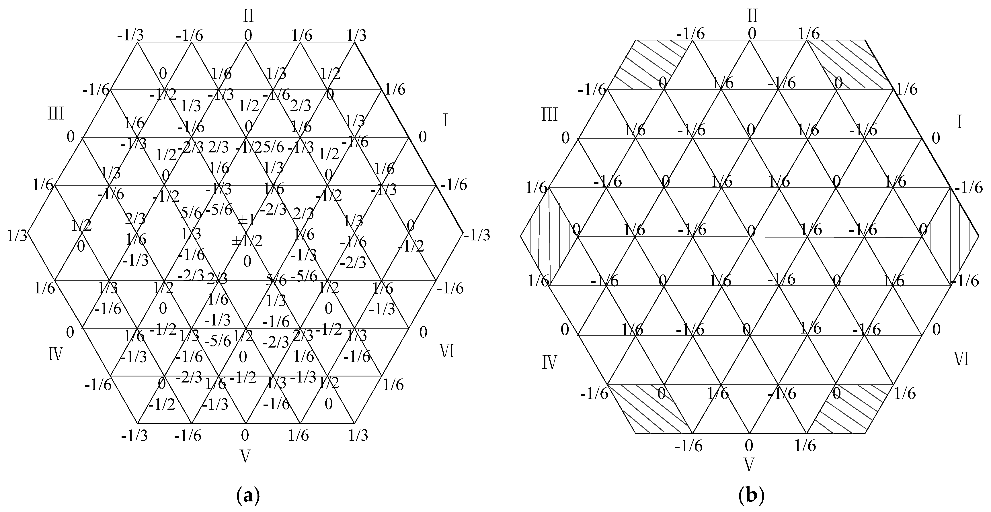
where uao, ubo, and uco are the output voltage of each phase, which are obtained by Equation (1). Their values are: Vdc, Vdc/2, 0. So, all of the values of UCMV can be calculated as: Vdc, 5Vdc/6, 2Vdc/3, Vdc/2, Vdc/3, Vdc/6, and 0. The common-mode voltage distribution of the five-level NPC/H bridge inverter is shown in Figure 5 (where the Vdc is omitted).
Figure 5a shows the traditional common-mode voltage distribution of the five-level NPC/H bridge inverter. In order to suppress the common-mode voltage of the system while not affecting the output performance of the inverter, this paper retains the vector that has the smallest common-mode voltage among all the redundant vectors. Additionally, the six vertex vectors of the outer hexagon are eliminated. So, the common-mode voltage distribution in Figure 5a can be simplified as shown in Figure 5b.
When the reference voltage is located in the shaded quadrangle of Figure 5b, the closest three voltage vectors are utilized in the synthesis. Thus, the common-mode voltage of the five-level NPC/H bridge inverter is suppressed to Vdc/6 and 0 while the output performance of the inverter is ensured.
4. The Proposed Dual-Pulse-Mapping Algorithm
In order to balance the DC-side capacitor voltages of a five-level NPC/H bridge inverter and suppress the CMV effectively at the same time, a dual-pulse-mapping algorithm is proposed. From the analysis above, we found that mapping (A) and (B) have the completely opposite influence on the DC-side capacitor voltages. When mapping (A) and (B) work, the influences of each vector on the three-phase midpoint potentials of capacitors are opposite. Thus, this paper selects mapping (A) and (B) to control the voltage alternately based on the six-segment SVPWM.
4.1. Vector Selection and Vector Duration Time
In this paper, the vector selection and calculation are based on the line-voltage coordinate system [6]. Assuming the three-phase reference voltages are Ua, Ub, and Uc, the a-b-c coordinate is converted to the ab-bc-ca line-voltage coordinate and unitized as Equation (3). The components of the reference voltage Vref on the axis ab, bc, and ca are Uab, Ubc, and Uca, respectively.
The per unit values of components are rounded up and down to an integer. In the equation, “floor” means rounding down to an integer and “ceil” represents rounding up to an integer.
All of the triangles can be separated into regular and inverted ones. If Fab + Fbc + Fca = −1, the end of the reference voltage vector is located in the regular triangle, and the coordinates of the three triangle vertexes (UA, UB, and UC) and the time duty ratio of three basic vectors are as follows.
If Fab + Fbc +Fca = −1, the end of the reference voltage vector is located in the inverted triangle. The coordinates and the time duty ratio are as follows.
After selecting the three basic vectors, it is essential to find all the switching states corresponding to each basic vector. (Sa, Sb, Sc) represents the switching states of basic vectors in the coordinate system. UX = (a, b, c) represents the coordinates of triangle-vertex vectors in the line-voltage coordinate system (where X = A, B, or C).
Equations (5)–(7) can quickly determine the triangle-vertex vectors and their time duty ratios. The relationship between common-mode voltage and switching states is obtained by Equations (1) and (2) as the following:
The dual-pulse-mapping algorithm proposed in this paper utilizes Equation (8) to select the vectors that have the smallest CMV among redundant vectors.
4.2. Voltage Balancing Algorithm
Based on the traditional SVPWM, this paper presents a new algorithm, called the dual-pulse-mapping algorithm, which is composed of six segments. The first three segments are controlled by pulse mapping (A), and the other segments are controlled by mapping (B). At the same time, the regulating factor k is adopted for each vector. According to the midpoint potentials of the three phases, adjusting the working time of each vector under the two pulse mappings can balance the capacitor voltages effectively and stably. Taking sector I as example, the vectors with the smallest value of CMV are shown in Figure 6.
We take the 13th triangle in Figure 6 as an example to explain how the dual-pulse mapping works. Because the reference voltage is in the 13th triangle, the vector synthesizing sequence is showing as Figure 7.
As shown in Table 2 and Table 3, the pulse mappings (A) and (B) have the opposite effect on the midpoint potential. Based on this, the regulating factors ka and kc are adopted. Assuming that the working time of the three vectors are T1, T2, and T3, the working time of the six segments is assigned as Figure 8.
If the midpoint potential of phase A is equal to Vdc/2, then ka is 0.5. If the midpoint potential of phase A is higher than Vdc/2, we only need to reduce the value of ka to <0.5, for example 0.4, in order to increase the working time of 10-2 under mapping (B) (because the time if the follow current’s state is much smaller than the sampling time and a follow current also exists when using pulse mapping (B), so this state will not be taken into consideration). It is all the same when the midpoint potential of phase A is lower than Vdc/2. By adjusting the operating time of 10-2 under the two kinds of pulse mappings, the midpoint potential of phase A will be balanced.
5. Simulation Verification and Analysis
In order to show the performance of the proposed method, simulation studies were carried out in the MATLAB/Simulink software environment. The condition were set as follows: the DC-side voltage equals 1000 V, the rated DC-side capacitor voltages Vdc equal 500 V, the DC capacitances are 3300 μF, the output voltage frequency f is 50 Hz, the load power factor cosφ is 0.985, and its impedance Z equals 26.43.
5.1. Simulation Results of the Conventional SVPWM Strategy
Figure 9a shows the three-phase midpoint potentials (which are defined as the difference values between the midpoint potentials of the unbalanced three-phase capacitors and the midpoint potentials of the balanced capacitors) when using the conventional SVPWM, which only adopts mapping (A). The DC-side voltage equals 1000 V, so the midpoint potentials of the balanced capacitors are 500 V. The midpoint potentials of the three-phase capacitors are continuously increased from 0 V to 500 V, which is consistent with the theoretical analysis. Figure 9b shows the line voltage between phase A and phase B; the nine-level line voltage attenuates to five-level as time goes by. When the modulation index m has high values, the midpoint current of the inflow capacitor is large, and the voltage of the capacitor changes greatly. Therefore, the midpoint potential of the capacitor rises rapidly. On the contrary, when m has low values, the midpoint potential of the capacitor rises slowly.
The line voltage between phase A and phase B is degraded to five-level from the original nine-level. The imbalanced DC-side voltages inject harmonics into the output voltage of the inverter, thereby distorting the output voltage waveform. If the inverter continues to work in an unbalanced capacitor voltage state, the power electronics in the system will be unevenly pressed or will even break down, and eventually the entire system will not work properly.
5.2. Simulation Results with the Proposed Dual-Pulse-Mapping Strategy
The proposed dual-pulse-mapping strategy was also analyzed using simulations, and the simulation parameters were the same as those for the simulations of the conventional SVPWM. Figure 10 shows the three-phase current, the midpoint potentials of the three-phase DC-side capacitors, the line voltage between phase A and phase B, and the common-mode voltage under the modulation index of 0.4 and 0.9 when the power factor of the load equals 0.984.
According to the Figure 10, under the modulation index of 0.4 and 0.9, the proposed dual-pulse-mapping strategy could control the operation of the inverter stably. The midpoint potentials of the three-phase DC-side capacitors fluctuate within ±3 V, which indicates that the proposed algorithm can effectively balance the midpoint potentials of DC-side capacitors. The largest ripple in the common voltage is 1/6Vdc, which means that the common voltage has effectively been suppressed.
5.3. Simulation Results of Dynamic Performance
We performed a simulation with the conventional strategy in which the modulation index was 0.9, the power factor was 0.984, and the pre-charged voltage of the DC-side capacitor was 500 V. When the midpoint potentials of the DC-side capacitors reached Vdc/2, the proposed dual-pulse-mapping strategy was used to balance the voltage. Figure 11 shows the simulation diagram of the midpoint potentials of the DC-side capacitors, the voltages of phase A’s two capacitors, and the line voltage between phase A and phase B. Under the pulse mapping (A), the midpoint potentials of the three-phase capacitors rise rapidly from 0 V to 500 V and the two capacitor voltages of phase A also change from 500 V to 0 V and 1000 V, respectively. The line voltage between phase A and phase B degrades to five-level. Then, the dual-pulse-mapping algorithm was adopted. The midpoint potentials of three-phase capacitors return to a balanced state and the line voltage also returns to nine-level. The two capacitor voltages of phase A change from 0 V and 100 V to 50 V. These simulation results show that the proposed algorithm has intelligent dynamic performance.
6. Experimental Results
In order to further verify the effectiveness of the proposed control algorithm for balancing DC-side (Direct Current) capacitor voltages and the suppression of the common-mode voltage and its dynamic response capability, a three-phase, five-level NPC/H Bridge inverter with an RL load experimental platform was built as shown in Figure 12. The structure is composed of a 12-pulse uncontrolled rectifier and a five-level NPC/H-bridge-type inverter. The basic parameters of the experiment are shown in Table 4.
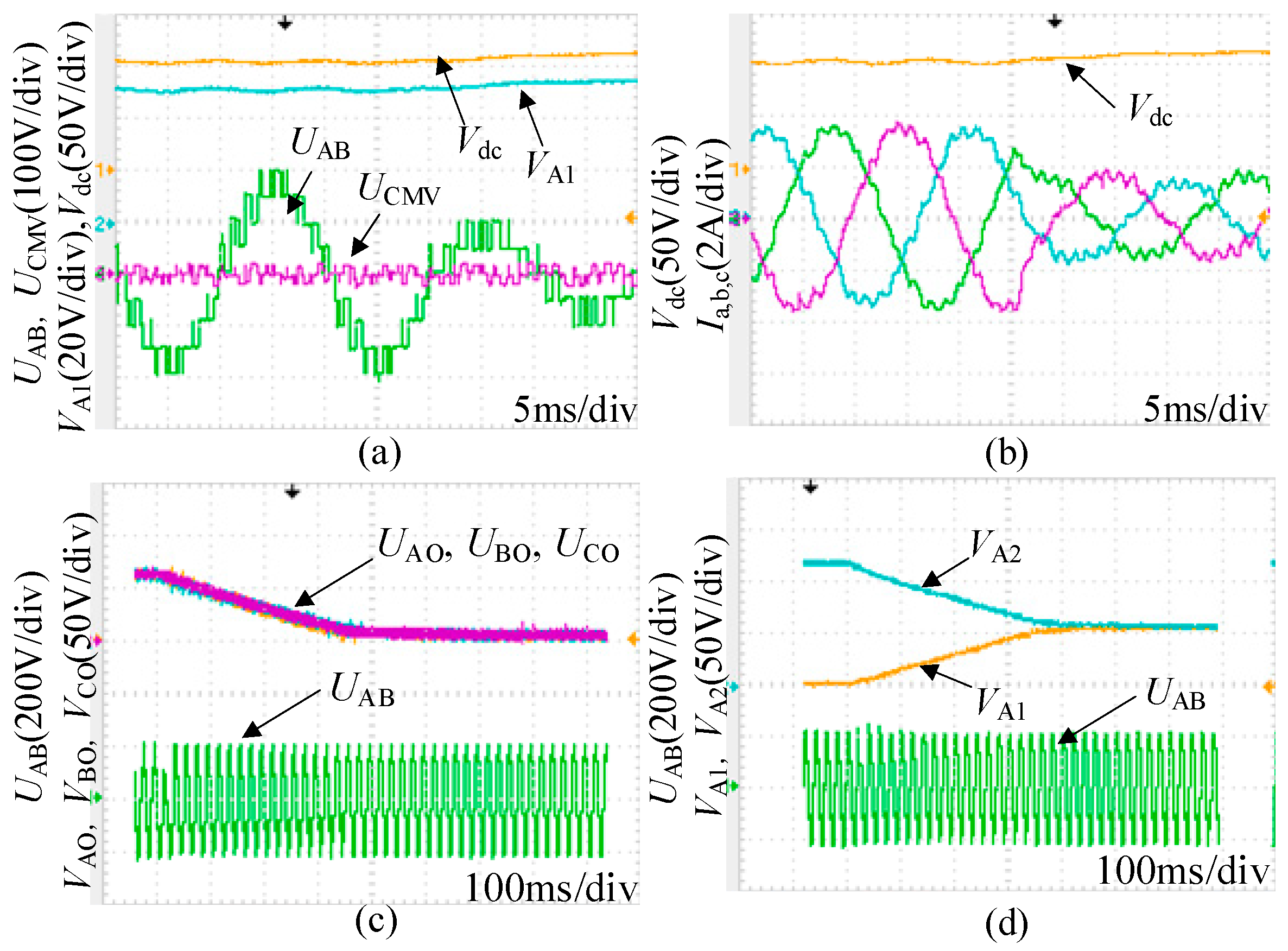
In Figure 13a,b, the DC-side capacitor voltages’ fluctuations are very small regardless of whether the reference voltage locates in the high- or low-modulation index region, and the common-mode voltage of the system is suppressed at the −Vdc/6, 0, Vdc/6. This proves that the dual-pulse-mapping algorithm controls the stable operation of the three-phase, five-level NPC/H-bridge inverter. Figure 13c,d show the harmonic analysis of the line voltage. It can be seen that, when the modulation index m is 0.9 and 0.4, the THD is 17.8% and 35.0%, respectively, which means that the output performance of the algorithm is the same as that of traditional SVPWM.
The pulse-width modulations (PWMs) of Sa1, Sa2, Sa3, and Sa4 in phase A are shown in Figure 14. The switching frequencies of the four switches in phase A were calculated approximately during 250~350 Hz, with a modulation index m of 0.4 and 0.9. The higher the modulation index is, the lower the switching frequency of each switch is. Phase B and C are both the same. Compared with the traditional SVPWM, the switching frequency of each switch just a little higher.
Figure 15a,b show the experimental waveforms of the dynamic response when the reference voltage modulation index suddenly decreases. The modulation index changes from m = 0.9 to m = 0.4. The line voltage and phase currents respond immediately during a very short time. The capacitor voltage is still balanced but has a little increase because of the uncontrolled rectifier.
In order to verify the strong self-balancing property of the algorithm, the conditions were set as follows: in the beginning, the modulation index was m = 0.9, and the values of regulating factors were all 0.5, which means that the dual-pulse-mapping algorithm was equivalent to a common six-segment SVPWM. Under the mapping (A), the midpoint potentials VAO, VBO, and VCO rise quickly and achieve the maximum Vdc/2 after some time. The line voltage also degenerates to five-level from nine-level. The inverter works under an unstable condition. Then, the dual-pulse-mapping algorithm was adopted. In Figure 15c, the midpoint potentials of the three-phase capacitors return to a balanced state after a short time. The line voltage also returns to nine-level. The two capacitor voltages in phase A change from 0 V and 100 V to 50 V in Figure 15d.
7. Conclusions
In this paper, the balance of the midpoint potentials of three-phase DC-side capacitors and the suppression of common-mode voltage were studied in a three-phase, five-level NPC/H-bridge inverter. A dual-pulse-mapping algorithm was proposed based on the characteristics of this topology. In combination with the traditional six-segment SVPWM, the proposed algorithm selectively uses the two pulse mappings that have the opposite effects on the midpoint potentials of the capacitors. The simulation and experimental results show that the proposed algorithm can balance the midpoint potentials perfectly and can suppress the common-mode voltage effectively. Based on the dynamic experiments, we can conclude that the proposed algorithm has a good capability to respond and the output performance is as good as that of the traditional SVPWM. Compared with the hardware balancing method, the volume and the cost of the system are both reduced. So, the proposed algorithm has a certain significance for cascaded NPC/H-bridge multilevel topology research. In high-voltage and high-power applications, the NPC/H bridge topology will be more suitable with the proposed algorithm.
Author Contributions
Z.S. put forward the main idea of this paper. K.Z. and Q.C. performed the data analysis and the simulations/experiments. M.W. and Z.L. assisted with the idea’s development and the paper’s writing.
Funding
This research was funded by National Key R&D Program of China, grant number is 2016YFB 0900400.
Conflicts of Interest
The authors declare no conflict of interest.
References
- Wu, B. High Power Converters and AC Drives; IEEE Press/Wiley: New York, NY, USA, 2006. [Google Scholar]
- Rodgriguez, J.; Lai, J.S.; Peng, F.Z. Multilevel inverters: A survey of topologies, controls and applications. IEEE Trans. Ind. Appl. 2002, 49, 724–738. [Google Scholar]
- Saeedifard, M.; Barbosa, P.M.; Steimer, P.K. Operation and control of a hybrid seven-level converter. IEEE Trans. Power Electron. 2012, 27, 652–660. [Google Scholar] [CrossRef]
- Kokila, A.; Kumar, V.S. Comparison of SPWM and SVPWM control techniques for diode clamped multilevel inverter with photovoltaic system. In Proceedings of the 2018 4th International Conference on Electrical Energy Systems (ICEES), Chennai, India, 7–9 February 2018; pp. 234–241. [Google Scholar]
- Yang, P.; Li, C.; Lan, Z. Investigation on the subsection synchronous modulation strategy for high power NPC/H-bridge inverter. In Proceedings of the IEEE 8th International Power Electronics and Motion Control Conference (IPEMC-ECCE Asia), Hefei, China, 22–26 May 2016. [Google Scholar]
- Chang, H.; Wei, R.; Ge, Q.; Wang, X.; Zhu, H. Comparison of SVPWM for five level NPC/H-Bridge inverter and traditional five level NPC inverter based on line-voltage coordinate system. In Proceedings of the International Conference on Electrical Machines and Systems, Pattaya, Thailand, 25–28 October 2015; pp. 574–577. [Google Scholar]
- Gong, Z.; Wu, X.; Dai, P.; Zhu, R. Modulated model predictive control for MMC-based active frontend rectifiers under unbalanced grid conditions. IEEE Trans. Ind. Electron. 2019, 66, 2398–2409. [Google Scholar] [CrossRef]
- Rendusara, D.A.; Cengelci, E.; Enjeti, P.N.; Stefanovic, V.R.; Victor, R.; Gray, J.W. Analysis of common mode voltage — neutral shift in medium voltage PWM adjustable speed drive (MV-ASD) systems. IEEE Trans. Power Electron. 2014, 29, 6281–6292. [Google Scholar]
- Gong, Z.; Zhang, H.; Dai, P.; Sun, N.; Li, M. A low-cost phase-angle compensation method for the indirect matrix converters operating at the unity grid power factor. IEEE Trans. Power Electron. 2019. [Google Scholar] [CrossRef]
- Sun, L.; Wu, L.Z.; Ma, W.; Fei, X.; Cai, X.; Zhou, L. Analysis of the DC-link capacitor current of power cells in cascaded H-Bridge inverters for high-voltage drives. IEEE Trans. Power Electron. 2014, 29, 6281–6292. [Google Scholar] [CrossRef]
- Wu, C.M.; Lau, W.H.; Chung, H. A five-level neutral-point-clamped H-bridge PWM inverter with superior harmonic suppression: A theoretical analysis. In Proceedings of the 1999 IEEE International Symposium on Cirsuits and Systems, Orlando, FL, USA, 30 May–2 June 1999; Volume 5, pp. 198–201. [Google Scholar]
- Chen, Z.Y.; Wu, B. A Novel Switching Sequence Design for Five-Level NPC/H-Bridge Inverters With Improved Output Voltage Spectrum and Minimized Device Switching Frequency. IEEE Trans. Power Electron. 2017, 22, 2138–2145. [Google Scholar] [CrossRef]
- Shen, J.; Schroder, S.; Gao, J.P.; Qu, B. Impact of DC-Link Voltage Ripples on the Machine-Side Performance in NPC H-Bridge Topology. IEEE Trans. Ind. Appl. 2016, 52, 3212–3223. [Google Scholar] [CrossRef]
- Rojas, C.A.; Kouro, S.; Edwards, D.; Wu, B. Five-level H-bridge NPC central photovoltaic inverter with open-end winding grid connection. In Proceedings of the 40th Annual Conference of the IEEE Industrial Electronics Society (IECON), Dallas, TX, USA, 30 October–1 November 2014; pp. 4622–4627. [Google Scholar]
- Hotait, H.A.; Massoud, A.M.; Finney, S.J.; Williams, B.W. Capacitor Voltage Balancing Using Redundant States of Space Vector Modulation for Five-level Diode Clamped Inverter. IET Power Electron. 2010, 3, 292–313. [Google Scholar] [CrossRef]
- Qin, J.C.; Saeedifard, M. Capacitor Voltage Balancing of a Five-level Diode-Clamped Converter Based on a Predictive Current Control Strategy. In Proceedings of the 26th Annual IEEE Applied Power Electronics Conference and Exposition, Fort Worth, TX, USA, 6–10 March 2011; pp. 1656–1660. [Google Scholar]
- Long, L.Z.; Zhang, Y.G.; Kuang, G.J. A Modified Space Vector Modulation Scheme to Reduce Common Mode Voltage for Cascaded NPC/H-bridge Inverter. In Proceedings of the IEEE 7th International Power Electronics and Motion Control Conference (ECCE), Harbin, China, 25 June 2012; pp. 1837–1841. [Google Scholar]
- Gong, Z.; Dai, P.; Wu, X.J.; Deng, F.J.; Liu, D.; Chen, Z. A Hierarchical Model Predictive Voltage Control for NPC/H-Bridge Converters with a Reduced Computational Burden. J. Power Electron. 2017, 17, 136–148. [Google Scholar] [CrossRef] [Green Version]
Figure 1.
A diagram of a five-level, neutral-point-clamped (NPC)/H-bridge inverter’s main circuit.
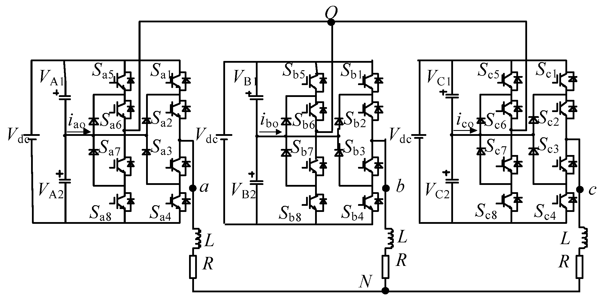
Figure 2.
The circuit of pulse mapping 1.
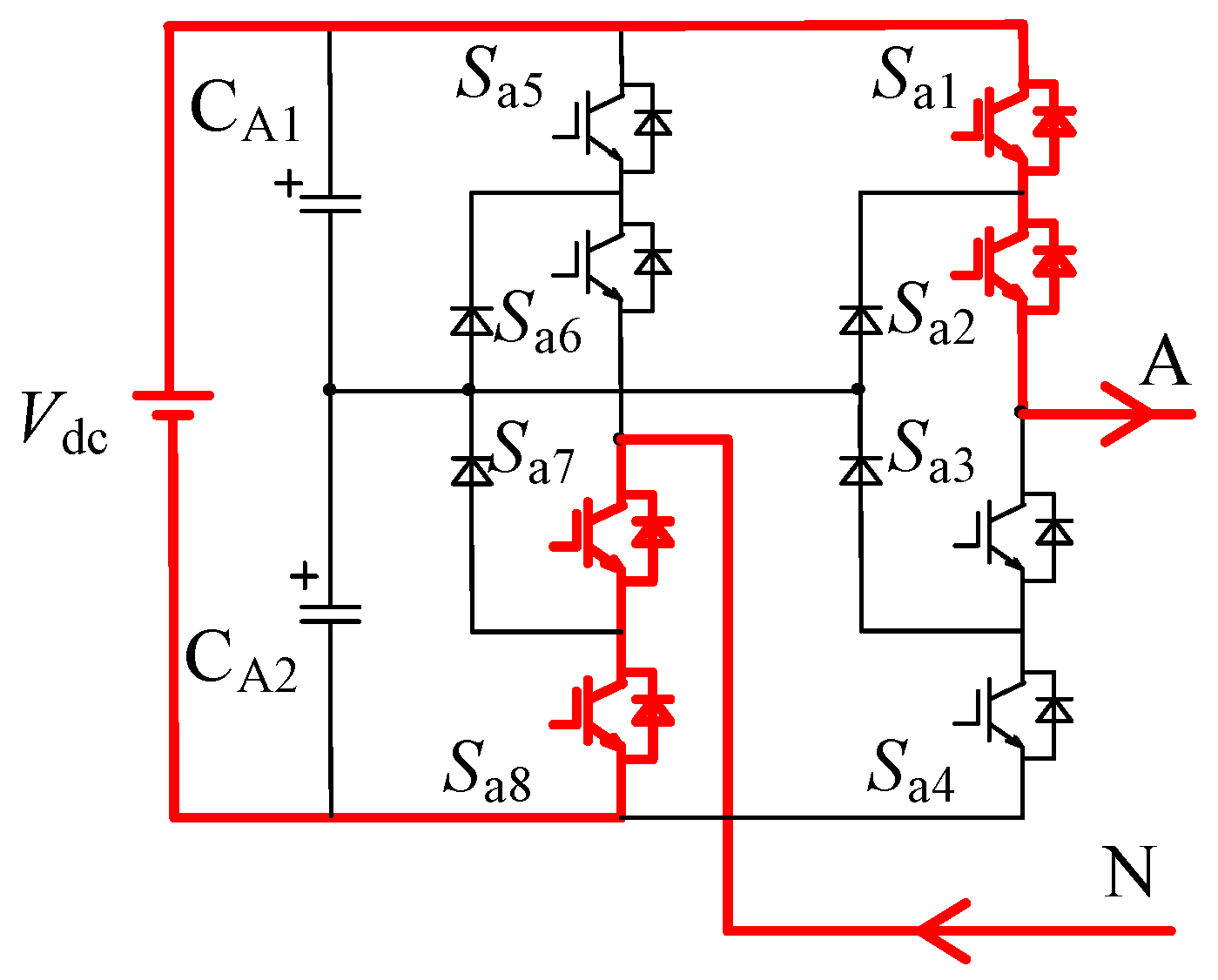
Figure 3.
The circuit of pulse mapping 2.

Figure 4.
The circuit of pulse mapping 3.
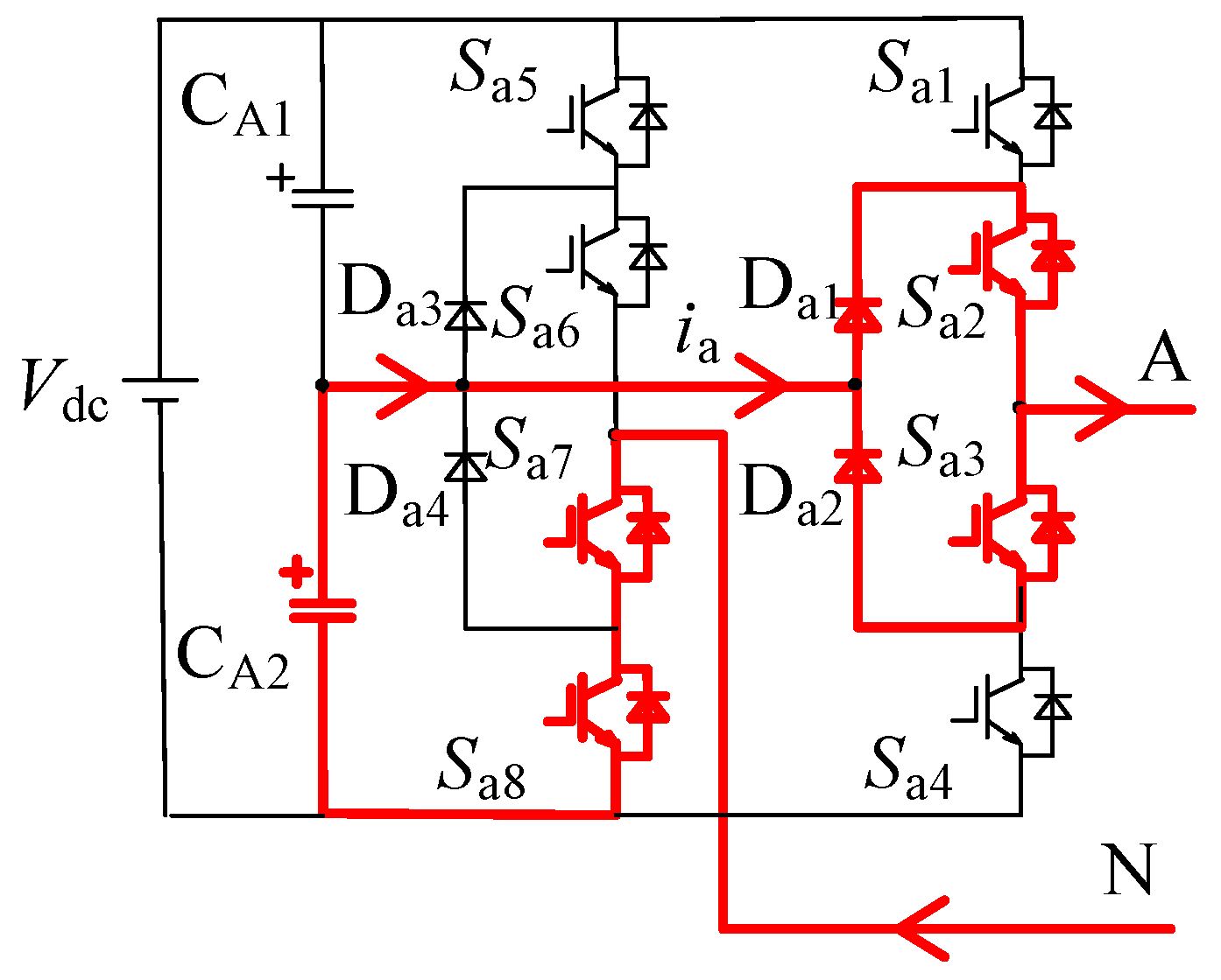
Figure 5.
The common-mode voltage distribution. (a) Common-mode-voltage distribution diagram of traditional strategy; and (b) Common-mode-voltage distribution diagram of proposed strategy.
Figure 5.
The common-mode voltage distribution. (a) Common-mode-voltage distribution diagram of traditional strategy; and (b) Common-mode-voltage distribution diagram of proposed strategy.

Figure 6.
The vectors with the minimum common-mode voltage (CMV) in Sector I.

Figure 7.
The vector synthesizing sequence of dual-pulse mapping strategy.
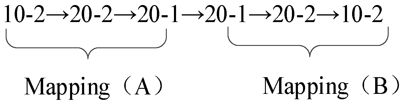
Figure 8.
The assigned working time of sex segments.
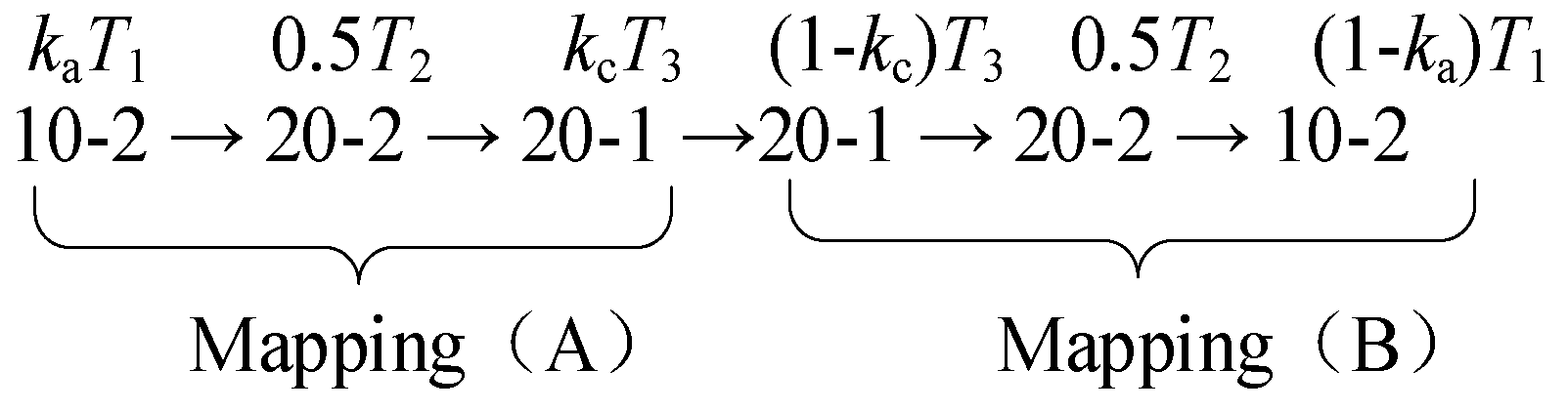
Figure 9.
The inverter without capacitor voltage control. (a) Midpoint Potential of three phases; and (b) Line voltage and common mode voltage.
Figure 9.
The inverter without capacitor voltage control. (a) Midpoint Potential of three phases; and (b) Line voltage and common mode voltage.

Figure 10.
The simulation waveforms under the algorithm. (a) The three-phase current, midpoint potentials, line voltage between phase A and phase B, and common-mode voltage when m is 0.4; and (b) The three-phase current, midpoint potentials, line voltage between phase A and phase B, and common-mode voltage when m is 0.9.
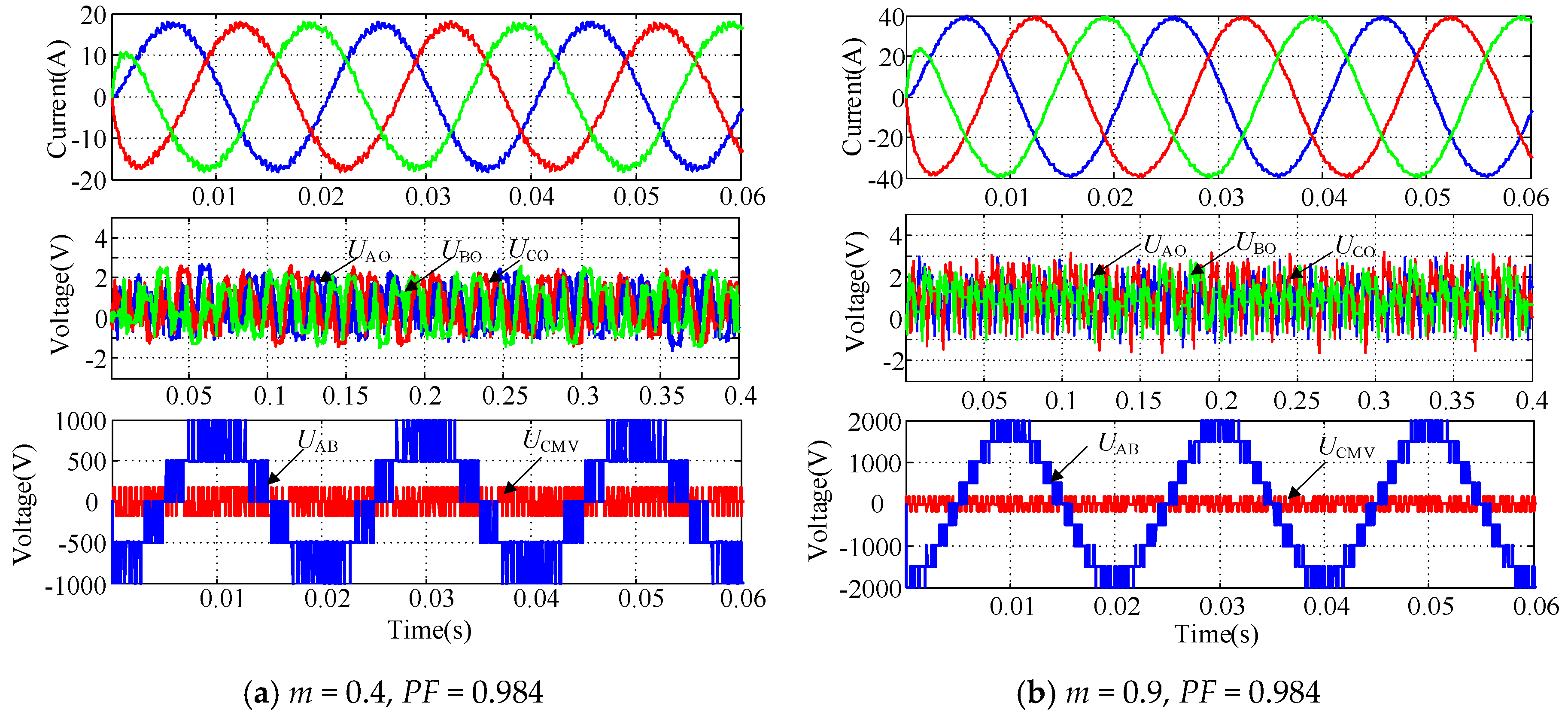
Figure 11.
The simulation waveform of dynamic performance.
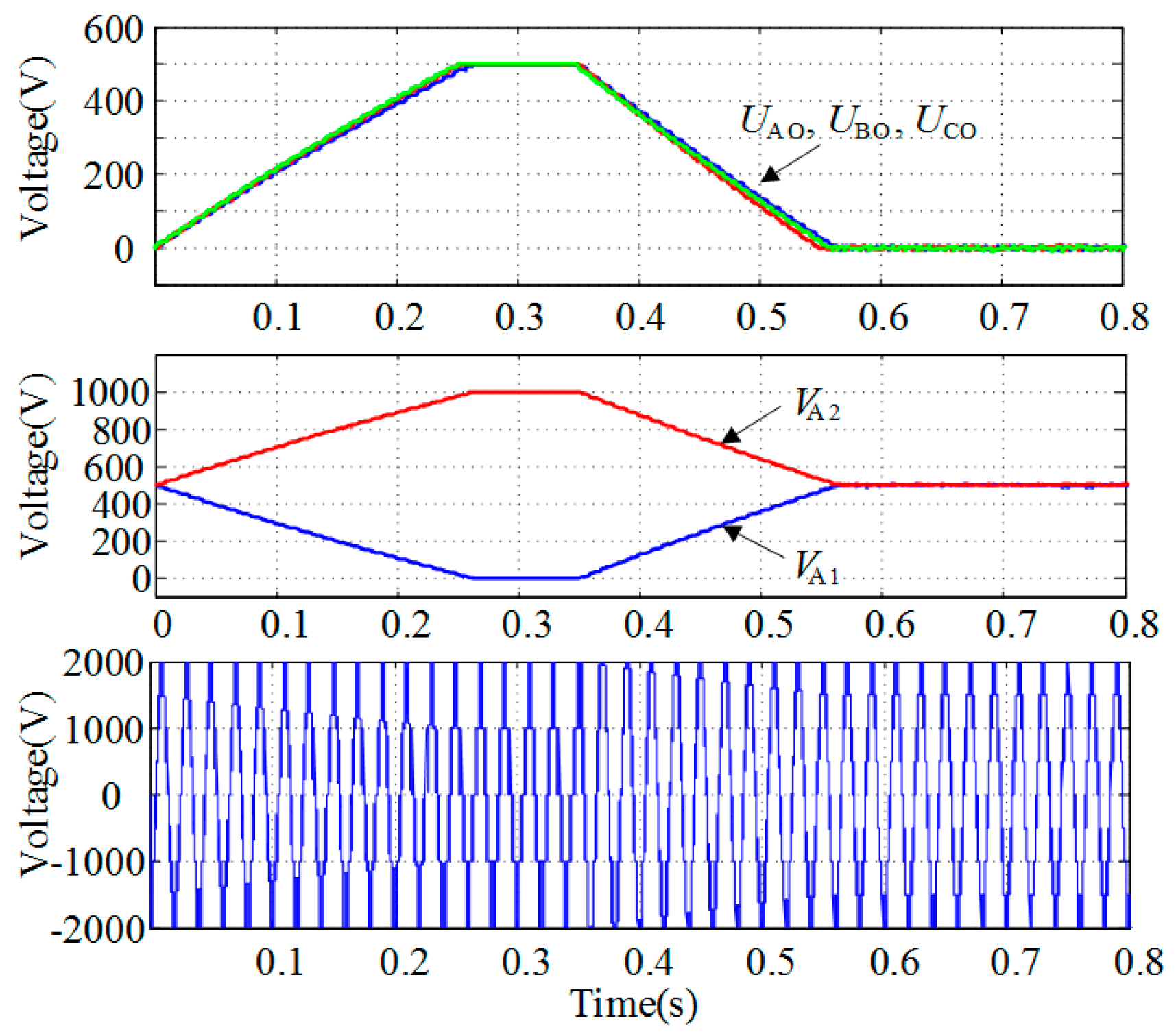
Figure 12.
The experimental platform.

Figure 13.
The experimental results of steady-state operation. (a) The DC-side voltage, the capacitance voltage of phase A, line voltage between phase A and phase B, and common-mode voltage when m is 0.9; (b) The DC-side voltage, the capacitance voltage of phase A, line voltage between phase A and phase B, and common-mode voltage when m is 0.4; (c) The harmonic analysis of the line voltage when m is 0.9; and (d) The harmonic analysis of the line voltage when m is 0.4.
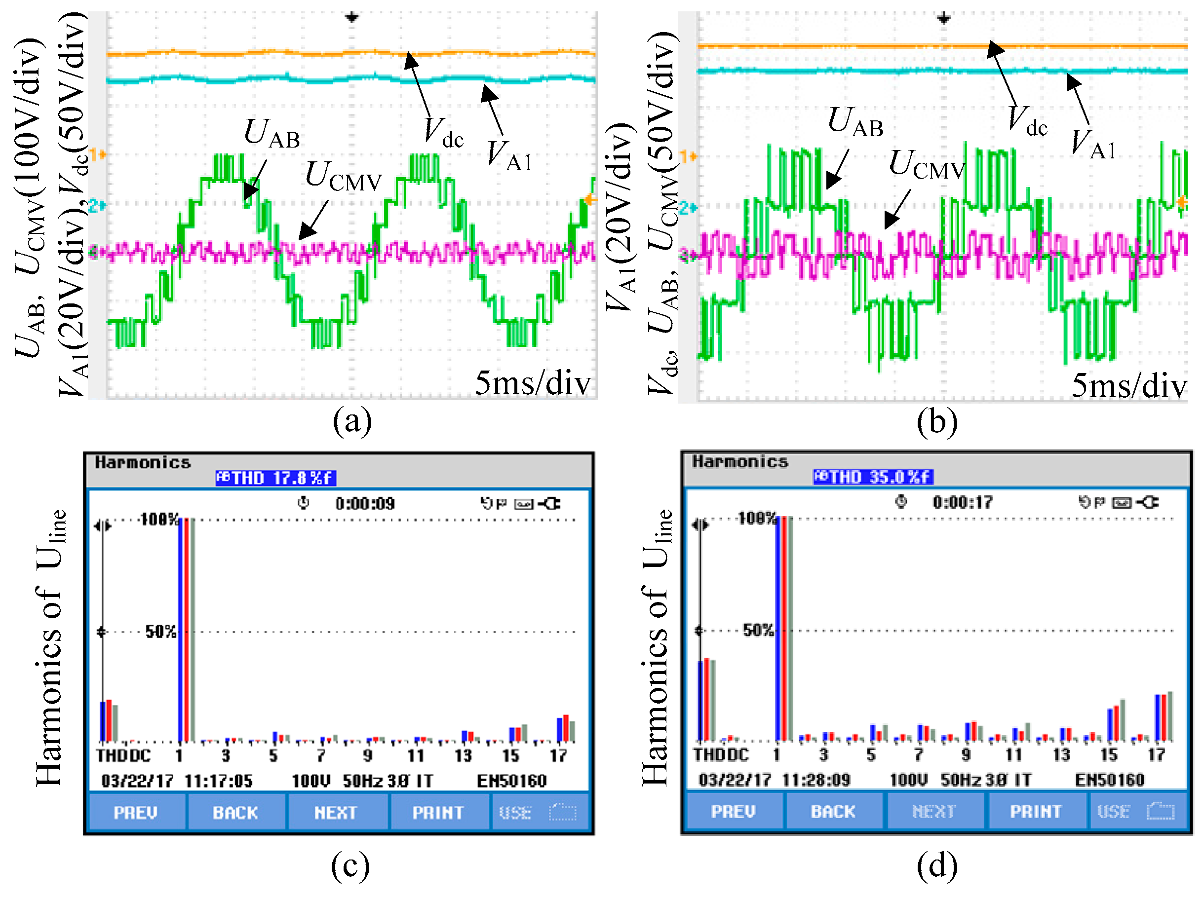
Figure 14.
The pulse width modulations (PWMs) of phase A when m = 0.4 and m = 0.9.
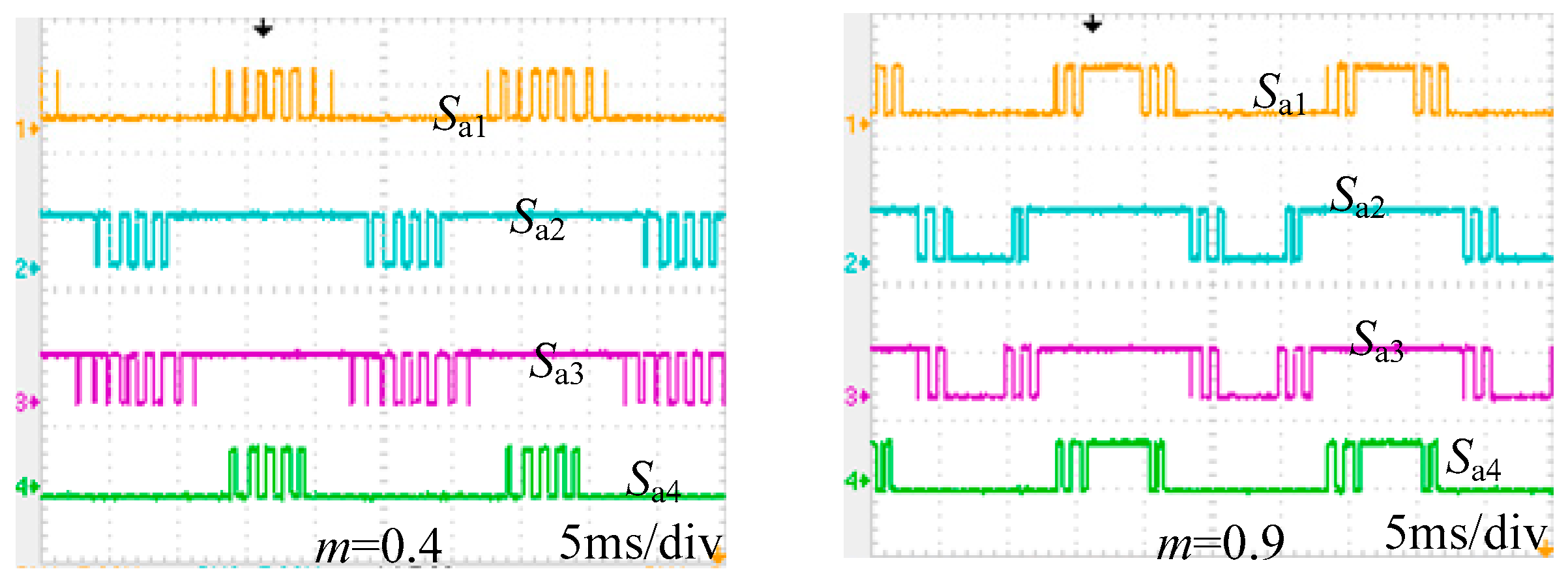
Figure 15.
The experimental results of dynamic performance. (a) The DC-side voltage, the capacitance voltage of phase A, line voltage between phase A and phase B, and common-mode voltage with changing m; (b) The DC-side voltage and the currents of three-phase with changing m; (c) The midpoint potentials of three-phase and the line voltage between phase A and phase B after dual-pulse mapping strategy started to work; and (d) The two capacitor voltages in phase A after dual-pulse mapping strategy started to work.

Table 1.
The switching states and pulse mappings.
| Switching State Sx | Pulse Mapping Number | Sx1, Sx2, Sx3, Sx4, Sx5, Sx6, Sx7, Sx8 | Phase Voltage uxo |
|---|---|---|---|
| 2 | 1 | 11000011 | Vdc |
| 1 | 2 | 11000110 | Vdc/2 |
| 3 | 01100011 | ||
| 0 | 4 | 11001100 | 0 |
| 5 | 01100110 | ||
| 6 | 00110011 | ||
| −1 | 7 | 01101100 | −Vdc/2 |
| 8 | 00110110 | ||
| −2 | 9 | 00111100 | −Vdc |
Table 2.
Changes in midpoint potential in pulse mapping 2, 3, 7, and 8 with different direction currents.
Table 2.
Changes in midpoint potential in pulse mapping 2, 3, 7, and 8 with different direction currents.
| Switching State Sx | Pulse Mapping Number | Sx1, Sx2, Sx3, Sx4, Sx5, Sx6, Sx7, Sx8 | Direction of ia | Midpoint Potential |
|---|---|---|---|---|
| 1 | 2 | 11000110 | + | ↑ |
| − | ↓ | |||
| 3 | 01100011 | + | ↓ | |
| − | ↑ | |||
| −1 | 7 | 01101100 | + | ↑ |
| − | ↓ | |||
| 8 | 00110110 | + | ↓ | |
| − | ↑ |
Table 3.
The two pulse mappings of the five-level NPC/H-Bridge inverter.
| State | (A) | (B) |
|---|---|---|
| 2 | 11000011 | 11000011 |
| 1 | 11000110 | 01100011 |
| 0 | 01100110 | 01100110 |
| −1 | 01101100 | 00110110 |
| −2 | 00111100 | 00111100 |
Table 4.
The experimental parameters of the system.
| Parameters | Values |
|---|---|
| DC-side voltage Vdc | 100 V |
| Output voltage frequency fAC | 50 Hz |
| DC-side capacitance C | 3300 F |
| RL load | 26 Ω + 15 mH |
| Modulation index m | 0.9 and 0.4 |
| Switching frequency fs | 800 Hz |
© 2019 by the authors. Licensee MDPI, Basel, Switzerland. This article is an open access article distributed under the terms and conditions of the Creative Commons Attribution (CC BY) license (http://creativecommons.org/licenses/by/4.0/).
Share and Cite
MDPI and ACS Style
Wu, M.; Song, Z.; Lv, Z.; Zhou, K.; Cui, Q. A Method for the Simultaneous Suppression of DC Capacitor Fluctuations and Common-Mode Voltage in a Five-Level NPC/H Bridge Inverter. Energies 2019, 12, 779. https://doi.org/10.3390/en12050779
AMA Style
Wu M, Song Z, Lv Z, Zhou K, Cui Q. A Method for the Simultaneous Suppression of DC Capacitor Fluctuations and Common-Mode Voltage in a Five-Level NPC/H Bridge Inverter. Energies. 2019; 12(5):779. https://doi.org/10.3390/en12050779
Chicago/Turabian StyleWu, Ming, Zhenhao Song, Zhipeng Lv, Kai Zhou, and Qi Cui. 2019. "A Method for the Simultaneous Suppression of DC Capacitor Fluctuations and Common-Mode Voltage in a Five-Level NPC/H Bridge Inverter" Energies 12, no. 5: 779. https://doi.org/10.3390/en12050779
Note that from the first issue of 2016, this journal uses article numbers instead of page numbers. See further details here.