A Novel Multi-Element Resonant Converter with Self-Driven Synchronous Rectification


Department of Electronic Engineering, National Taiwan University of Science and Technology, Taipei 10607, Taiwan
*
Author to whom correspondence should be addressed.
Energies 2019, 12(4), 715; https://doi.org/10.3390/en12040715
Submission received: 27 January 2019
/
Revised: 19 February 2019
/
Accepted: 20 February 2019
/
Published: 22 February 2019
Abstract
:This paper proposes a novel multi-element resonant converter with self-driven synchronous rectification (SR). The proposed resonant converter can achieve a zero-voltage-switching (ZVS) operation from light load to full load, meanwhile, the zero-current-switching (ZCS) can achieve rectifiers of a secondary-side. Therefore, the switching losses can be significantly reduced. Compared with an LLC resonant converter, the proposed resonant converter can be effective to decrease the circulating energy through the primary-side of the transformer to output a load and provide a wide voltage gain range for over-current protection as well as decreasing the inrush current under the start-up condition. Moreover, the proposed converter uses a simple current detection scheme to control the synchronous rectification switches. A detailed analysis and design of this novel multi-element resonant converter with self-driven synchronous rectification is described. Finally, a DC input voltage of 380-VDC and an output voltage/current of 12-VDC/54-A for the resonant converter prototype is built to verify the theoretical analysis and performance of the proposed converter.
1. Introduction
Over the last ten years, LLC resonant converters have been widely used in the power supply industry because LLC resonant converters have a lot of advantages such as zero voltage switching (ZVS) on primary switches and the zero-current-switching (ZCS) can be achieved for the output rectifiers [1,2,3,4]. Moreover, the voltage stress ratings of the output rectifier only need two times the output voltage. Therefore, the secondary conduction losses can be significantly reduced. Furthermore, compared with a series resonant converter (SRC), a parallel resonant converter (PRC) and a series-parallel resonant converter (SPRC) [5,6], LLC resonant convertors allow a narrow switching frequency variation during the output load and input voltage variation [7,8]. Therefore, the LLC resonant converter can be simpler to design an electromagnetic interference (EMI) filter [9,10,11]. Unfortunately, the LLC resonant converter still has some issues to be solved [12,13], such as short output circuit and overload conditions will cause a large peak in current through the switches of the primary-side. Moreover, when the LLC resonant converter is used during start-up condition, the huge inrush current will cause destructive damage. Moreover, how to optimize driving synchronous rectifiers (SR) is still an important issue [14,15,16]. For instance, the current transformer (CT) to sense the current used to drive SRs has been proposed [17], but the magnetizing inductance of the transformer of the LLC resonant converter has been used for resonant inductance. Thus, the primary-side current of the transformer and the SRs current are out of phase. In contrast, when the CT sense the secondary-side current, which will cause large conduction losses through CT, so that it will reduce the conversion efficiency.
The multi-element resonant converter has been proposed to solve the above mentioned LLC resonant converter issues [18,19,20,21,22]. Since the voltage gain curve is relatively sharp and close to zero in resonant frequency, it can decrease the inrush current to solve short output circuit issues. On the other hand, the multi-element resonant tank can inject a third order harmonic, it can reduce the circulating current and decrease the conduction losses through switches of primary-side. Unfortunately, the SRs issues still cannot be solved. To overcome the above mention issues, a novel multi-element resonant converter with self-driven SRs is proposed in this paper. Compared to multi-element resonant converters, the proposed converter can use CT to sense primary-side current for SRs because the magnetizing inductance of the transformer is not used in the resonant tank and thus is relatively large, so that primary-side current and the SRs current are in phase. On the other hand, this proposed converter can also inject a third order harmonic current to reduce circulating energy losses. Moreover, compared with the LLC resonant converter, the voltage gain curve is sharp and close to zero in resonant frequency, which can decrease the inrush current to solve short output circuit issues. Similarly, the proposed converter can also utilize the ZVS technique to decrease the switching losses, resulting in a high efficiency of conversion. The operational principle of the proposed converter is analyzed, a prototype converter with a DC input voltage of 380-VDC and output voltage/current of 12-VDC/54-A has been built to verify the analytical results.
2. Circuit Description and Principle Operation
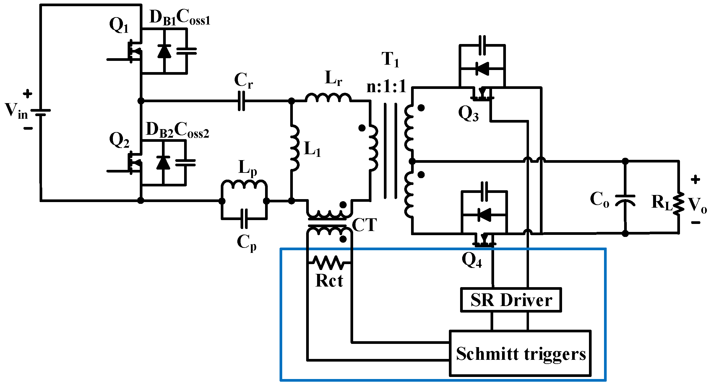
The proposed CLL-LC multi-element resonant converter is shown in Figure 1, where it is composed of Cr, Lr, L1, Lp and Cp. It should be noted that the magnetizing inductance of the transformer is not anticipated in the resonant tank, the magnetizing inductance is larger than other resonant components, so it can approximate an open-circuit. Therefore, in the proposed multi-element resonant converter, the primary-side current of the transformer and the secondary-side current are in phase, so that the CT can be used to detect the primary-side current signal through a secondary-side to drive SRs. DB1 and DB2 are the anti-paralleled diodes of the primary switches, Q3 and Q4 are SRs switches, and CO is the output capacitor.
Figure 2 depicts the key waveforms of the proposed CLL-LC multi-element resonant converter. There are eight states to complete a switching cycle. The conduction paths for each operating state are illustrated in Figure 3. In addition, the following simplifying assumptions are made:
- (1)
- All semiconductors, layout trace and the copper losses of the transformer are lossless.
- (2)
- The turns ratio of the transformer windings is n = N1/N2.
- (3)
- The output capacitance CO is large enough so that the output voltage VO is a constant value.
- (4)
- The magnetizing inductance of the transformer is large enough compared to other resonant components so it can approximate an open-circuit.
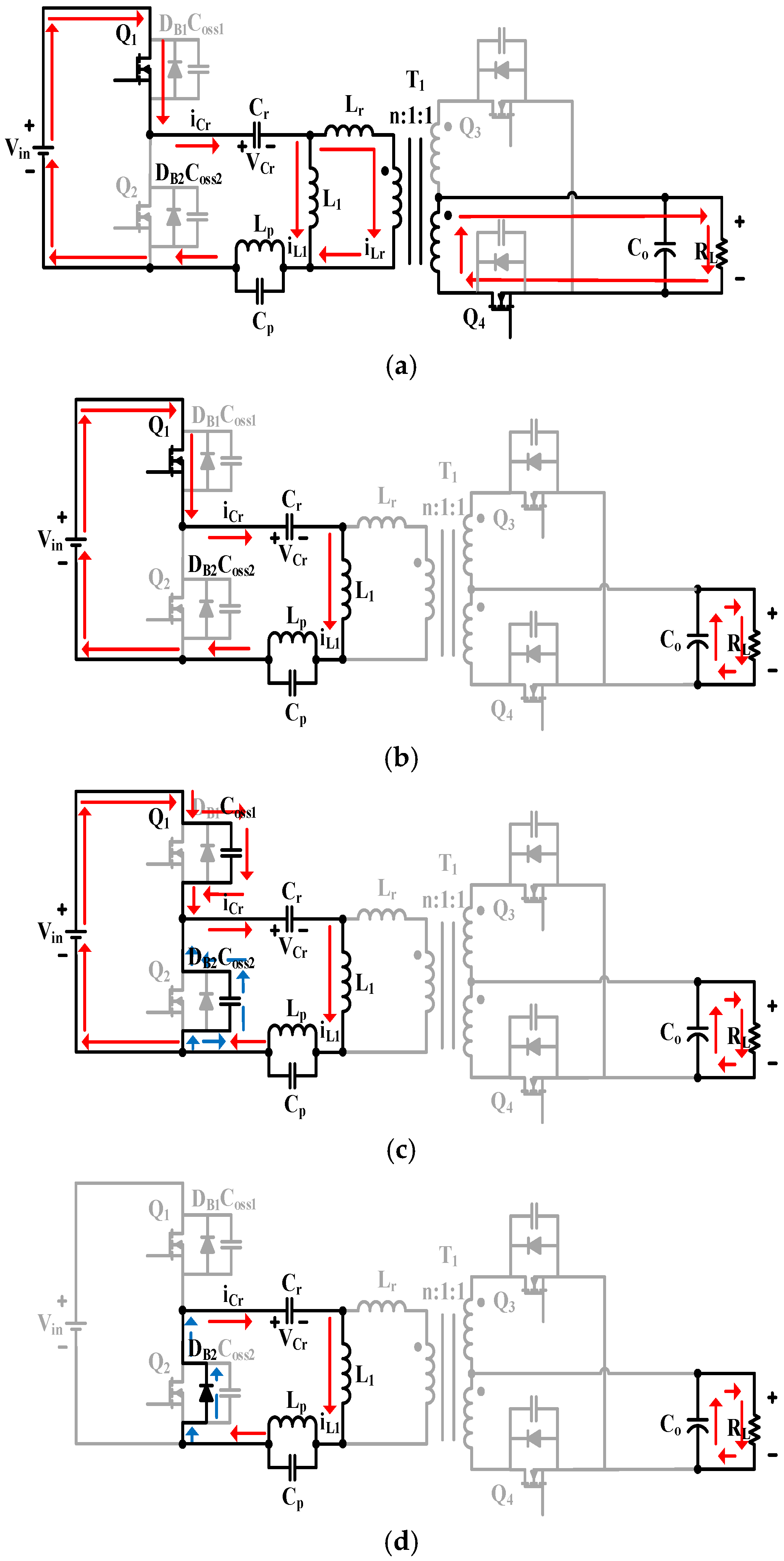
State 1: t0 < t < t1:
As shown in Figure 3, Q1 is turned on under the ZVS operating condition. Meanwhile, the synchronous rectifier Q3 is conducted. The resonant current iCr is increased and includes a third order harmonic current so that it can significantly reducethe circulating energy losses. On the other hand, the resonant inductor current iLr is equal to the primary-side of the transformer current and reflects the secondary-side though synchronous rectifier switch Q3. Therefore, the primary-side of the transformer and the secondary current is in phase. The voltage across the resonant inductor L1 is a positive direction, so the resonant inductor current iL1 is raised until iL1 is equal to iCr; this interval has ended.
State 2: t1 < t < t2:
During this mode, the resonant circuit is composed of Cr, Cp, L1 and Lp. At time t1, the resonant inductor current iL1 is the same as the resonant current icr. Therefore, there is no current transferred to the secondary side, so the synchronous rectifier Q3 is turned off and has achieved zero-current-switching (ZCS) and the output capacitance CO starts to provide the energy to the load at this moment.
State 3: t2 < t < t3:
The mode begins, when Q1 is turned off at t = t2. The resonant current iL1 will charge the junction-capacitors of Q1 and discharges the junction-capacitors of Q2 in the meantime. The output capacitance CO is still providing the energy to the load. When this interval has ended, the voltage across the resonant inductor L1 is equal to −nVo and the body diode of Q2 has conducted.
State 4: t3 < t < t4:
In this state, the body diode of Q2 has conducted, which carries the resonant inductor current iCr and the input inductor current iL1. The voltage across the input inductor L1 is about (VIN—VCp—VCr), so the input inductor current iL1 increases linearly. The output capacitors CO provide energy to the output load. Once this interval has ended, Q2 is turned on with the ZVS operating condition.
The equivalent circuit of the resonant tank in Figure 4 is for use by the First Harmonic Approximation (FHA) approach; the voltage gain M of the resonant tank can be derived and is given as follows:
where Rac is the AC equivalent load resistor and in order to simplify the analysis, the resonant inductor ratio is defined as K; the quality factor is defined as Q; the characteristic impedance is ZO, which can be expressed as follows:
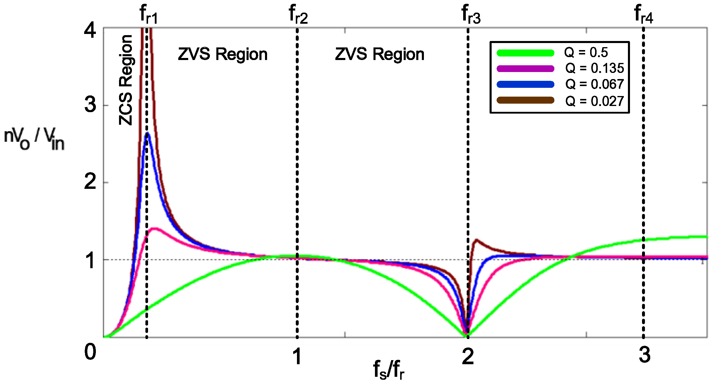
According to Equations (1) and (2), the voltage-gain curve is calculated and obtained by FHA using the equivalent impedance circuit in Figure 4. The voltage-gain with different Q factors in Figure 5 is shown, which includes factors for resonant impedance Zo and the equivalent output resistance Rac. Besides, the normalized frequency is adopted to express the voltage gain with switching frequency variation. There are four resonant frequencies included in this resonant tank, which have been simply expressed in Equation (3).
The voltage gain curve at near and below fr1 is similar to the LLC resonant converter, it can allow narrow switching frequency variation during the output load and input voltage variation. Meanwhile, the ZVS at the primary switches and ZCS at the secondary switches are both still achieved to reduce the switching loss and develop high efficiency conversion. Furthermore, since the input-voltage source is a square-wave on the proposed CLL-LC resonant converter it can be expanded to a fundamental and odd-term harmonics sine-wave by a Fourier analysis. The resonant tank, which employs the third resonant frequency fr3 can inject an extra high-order harmonic current to reduce the circulating current and to reduce conduction losses on the switches of the primary side and the secondary side. On the other hand, the voltage gain at fr2 is zero since the input impedance is infinite at fr2 so that it can make the inrush current decrease under the start-up condition to solve the short output circuit issue.
To further optimize the SRs driving issue, a novel multi-element resonant converter with self-driven SRs is proposed. In order to drive SR MOSFETs, the magnetizing inductance of the transformer is not used in the resonant tank and it is relatively large compared to other resonant components so that the primary-side current and the secondary-side current are in phase. The SR control circuit configuration is shown in Figure 6. A CT has been added at the primary side to sense the phase of the SR current through the primary transformer current. The Schmitt trigger circuit is used to detect the voltage polarity of the CT voltage and provide the SR driving signal to the SR driver. The waveform of the SR driving signal is shown in Figure 2. When the SR current starts to transfer energy to the load, the voltage of CT becomes positive, the output of Schmitt triggers the circuit to pull high. When the SR current decreases to a negative value, the output of Schmitt triggers the circuit to pull down. Therefore, the SRs driving signals can be obtained from Schmitt to trigger the circuit to turn on/off; a self-driven SR control can be achieved. Table 1 shows the voltage/current stress during each reactive element, capacitors and power devices. Table 2 compares the proposed converter with the conventional LLC converter. This proposed converter is especially suitable for applications under large-current load conditions, such as server power, because compared with the conventional LLC converter, this proposed converter has a simple and exact detecting circuit for the SR-driver. However, the resonant tank elements are more than those of the LLC converter, so that this proposed converter results in a lower power density.
3. Design Consideration and Experimental Results
A 650 W, 65 kHz 380-VDC/12-VDC multi-element CLL-LC resonant converter prototype was built to verify the theoretical analysis and the proposed design strategies. The commercial resonant controller IC L6599 was used for the proposed converter. In addition, we have used a compensator of 2-pole/1-zero to regulate the output voltage. The resonant parameters were designed as follows: Lr = 10.4 μH, Lp = 10 μH, Cr = 203.5 nF, Cp = 112 nF and L1 = 510 μH. The transformer turn ratio is 16:1:1. The core material is PC44. Lr is integrated with the transformer. The part numbers of the primary-side and secondary-side devices are IPP60R099CP and PSMN2R8-40PS, the resonant frequencies of the multi-element CLL-LC converter were designed and shown in Table 3.
Figure 7a,b shows the ZVS waveform of Q1 and Q2 at a full-load condition, Vds1 and Vds2 are the drain–source voltages of Q1 and Q2, respectively. Vgs1 and Vgs2 are the gate-source voltages of Q1 and Q2, ZVS is achieved at primary-side switches. Figure 8a,b shows the experimental waveforms of the CLL-LC converter under light-load and full-load conditions. Vgs3 and Vgs4 are the gate-source voltages of the SRs and ILrp is the primary-side resonant current.
In Figure 8a, since the amplitude of the current is lower at the light load, the Schmitt-trigger circuit is disabled. The driving signals of the SRs are non-activated at the light load, the SRs are turned off, which can also reduce the SRs driving loss since the percentage of SR driving loss at light load is significant. In Figure 8b, the Schmitt-trigger circuit is enabled when ILrp rises and reached Ith+. The SRs will turn on when ILrp drops and reaches Ith−. The SRs will turn off, since the Ith+ must be set larger than Ith− due to the operation restrictions of the Schmitt-trigger circuit. The turn-on signals of the SRs will act with a delay period. It can be also observed that the SR will turn off as the transformer enters the non-coupled region, which means that the secondary current is zero. Hence, ZCS is achieved. Figure 9a,b shows the experimental waveforms under the start-up condition, compared to the conventional LLC resonant converter, since the CLL-LC resonant converter employs ideally an infinite impedance at fo2. The inrush current can be effectively reduced by about 40% percent during the same start-up period.
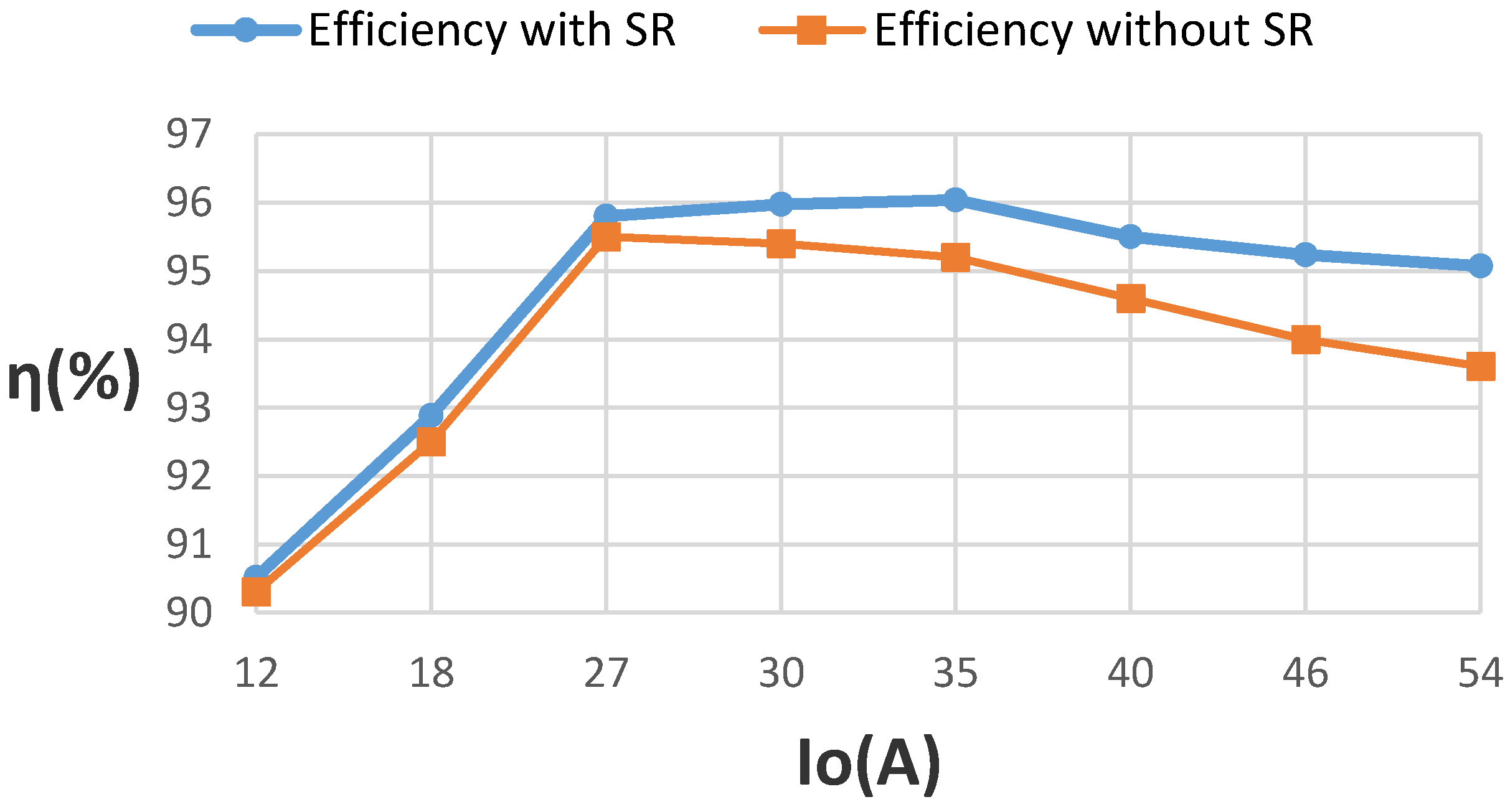
The efficiency of the proposed multi-element CLL-LC resonant converter is shown in Figure 10. The efficiency at a half load is 96.7%, and at a full load it is 96.1%. The peak efficiency is 96.04% at 65% load.
4. Conclusions
This paper has proposed a novel multi element CLL-LC resonant converter with a self-driven SR. The characteristics of the CLL-LC resonant converter have been analyzed and the operational regions of CLL-LC resonant converter have been discussed. The benefits of the third current harmonics injection and inrush current improvement under the start-up conditions have been discussed and verified. Meanwhile, an easily implemented current-type SR control scheme is proposed to achieve low SR losses. These features make the proposed multi-element CLL-LC resonant converter more suitable for applications with high-input and low-output voltages. The experimental results on a half-bridge multi resonant converter with SR are provided to verify the effectiveness of the proposed multi element CLL-LC resonant converter.
Author Contributions
Supervision, J.-Y.L.; Writing—Original Draft, S.-Y.L.; Writing—Review & Editing, Y.-F.L.
Funding
This research received no external funding.
Conflicts of Interest
The authors declare no conflict of interest.
References
- Tran, D.; Vu, N.; Choi, W. A Quasi-Resonant ZVZCS Phase-Shifted Full-Bridge Converter with an Active Clamp in the Secondary Side. Energies 2018, 11, 2868. [Google Scholar] [CrossRef]
- Bo, Y.; Lee, F.C.; Zhang, A.J.; Guisong, H. LLC Resonant Converter for Front End DC/DC Conversion. In Proceedings of the APEC 2002, Dallas, TX, USA, 10–14 March 2002; Volume 2, pp. 1108–1112. [Google Scholar]
- Choi, H. Analysis and Design of LLC Resonant Converter with Integrated Transformer. In Proceedings of the APEC 2007, Anaheim, CA, USA, 25 February–1 March 2007; pp. 1630–1635. [Google Scholar]
- Zhu, T.; Wang, J.; Ji, Y.; Liu, Y. A Novel High Efficiency Quasi-Resonant Converter. Energies 2018, 11, 1961. [Google Scholar] [CrossRef]
- Pernía, A.M.; Prieto, M.J.; Villegas, P.J.; Díaz, J.; Martín-Ramos, J.A. LCC Resonant Multilevel Converter for X-ray Applications. Energies 2017, 10, 1573. [Google Scholar] [CrossRef]
- Yu, A.; Zeng, X.; Xiong, D.; Tian, M.; Li, J. An Improved Autonomous Current-Fed Push-Pull Parallel-Resonant Inverter for Inductive Power Transfer System. Energies 2018, 11, 2653. [Google Scholar] [CrossRef]
- Fang, X. Efficiency-oriented optimal design of the LLC resonant converter based on peak gain placement. IEEE Trans. Power Electron. 2013, 28, 2285–2296. [Google Scholar] [CrossRef]
- Lu, B.; Liu, W.; Liang, Y.; Lee, F.C.; van Wyk, J.D. Optimal design methodology for LLC resonant converter. In Proceedings of the Twenty-First Annual IEEE Applied Power Electronics Conference and Exposition, Dallas, TX, USA, 19–23 March 2006; pp. 533–538. [Google Scholar]
- Fei, C.; Li, Q.; Lee, F.C. Digital Implementation of Adaptive Synchronous Rectifier (SR) Driving Scheme for High-Frequency LLC Converters With Microcontroller. IEEE Trans. Power Electron. 2018, 33, 5351–5361. [Google Scholar] [CrossRef]
- Fang, Z.; Cai, T.; Duan, S.; Chen, C. Optimal design methodology for LLC resonant converter in battery charging applications based on time-weighted average efficiency. IEEE Trans. Power Electron. 2015, 30, 5469–5483. [Google Scholar] [CrossRef]
- Kim, D.K.; Moon, S.C.; Yeon, C.O.; Moon, G.W. High-efficiency LLC resonant converter with high voltage gain using an auxiliary LC resonant circuit. IEEE Trans. Power Electron. 2016, 31, 6901–6909. [Google Scholar] [CrossRef]
- Zhao, Z.; Xu, Q.; Dai, Y.; Yin, H. Analysis, Design, and Implementation of Improved LLC Resonant Transformer for Efficiency Enhancement. Energies 2018, 11, 3288. [Google Scholar] [CrossRef]
- Khalid, U.; Khan, M.M.; Khan, M.Z.; Rasool, M.A.U.; Xu, J. Pulse Width and Frequency Hybrid Modulated LLC Converter Adapted to Ultra Wide Voltage Range. Inventions 2018, 3, 77. [Google Scholar] [CrossRef]
- Xie, X.; Liu, J.; Poon, F.N.K.; Pong, M. A novel high frequency current-driven SR applicable to most switching topologies. IEEE Trans. Power Electron. 2001, 16, 635–648. [Google Scholar]
- Zhang, S.-H.; Wang, Y.-I.; Chen, B.; Han, F.-U.; Wang, Q.-I. Studies on a Hybrid Full-Bridge/Half-Bridge Bidirectional CLTC Multi-Resonant DC-DC Converter with a Digital Synchronous Rectification Strategy. Energies 2018, 11, 227. [Google Scholar] [CrossRef]
- Huang, D.; Fu, D.; Lee, F.C. High switching frequency, high efficiency CLL resonant converter with synchronous rectifier. In Proceedings of the 2009 IEEE Energy Conversion Congress and Exposition, San Jose, CA, USA, 20–24 September 2009; pp. 804–809. [Google Scholar]
- Chang, Y.-N.; Chan, S.-Y.; Cheng, H.-L. A Single-Stage High-Power Factor Converter with Synchronized Self-Excited Technique for LED Lighting. Energies 2018, 8, 1408. [Google Scholar] [CrossRef]
- Huang, D.; Fu, D.; Lee, F.C.; Fu, D. Classification and selection methodology for multi-element resonant converters. In Proceedings of the 2011 Twenty-Sixth Annual IEEE Applied Power Electronics Conference and Exposition (APEC), Fort Worth, TX, USA, 6–11 March 2011; pp. 558–565. [Google Scholar]
- Chen, M.; Wang, Y.; Yang, L.; Han, F.; Hou, Y.; Yan, H. A Variable-Structure Multi-Resonant DC–DC Converter with Smooth Switching. Energies 2018, 11, 2240. [Google Scholar] [CrossRef]
- Wang, C.; Yang, L.; Wang, Y.; Chen, B. A 1-kw CLTCL resonant DCDC converter with restricted switching loss and broadened voltage range. IEEE Trans. Power Electron. 2018, 33, 4190–4203. [Google Scholar] [CrossRef]
- Wang, Y.; Yang, L.; Han, F.; Tu, S.; Zhang, W. A Study of Two Multi-Element Resonant DC-DC Topologies with Loss Distribution Analyses. Energies 2017, 19, 1400. [Google Scholar] [CrossRef]
- Fu, D.; Lee, F.C.; Liu, Y.; Xu, M. Novel multi-element resonant converters for front-end dc/dc converters. In Proceedings of the 2008 IEEE Power Electronics Specialists Conference, Rhodes, Greece, 15–19 June 2008; pp. 250–256. [Google Scholar]
Figure 1.
The proposed CLL-LC multi-element resonant converter.
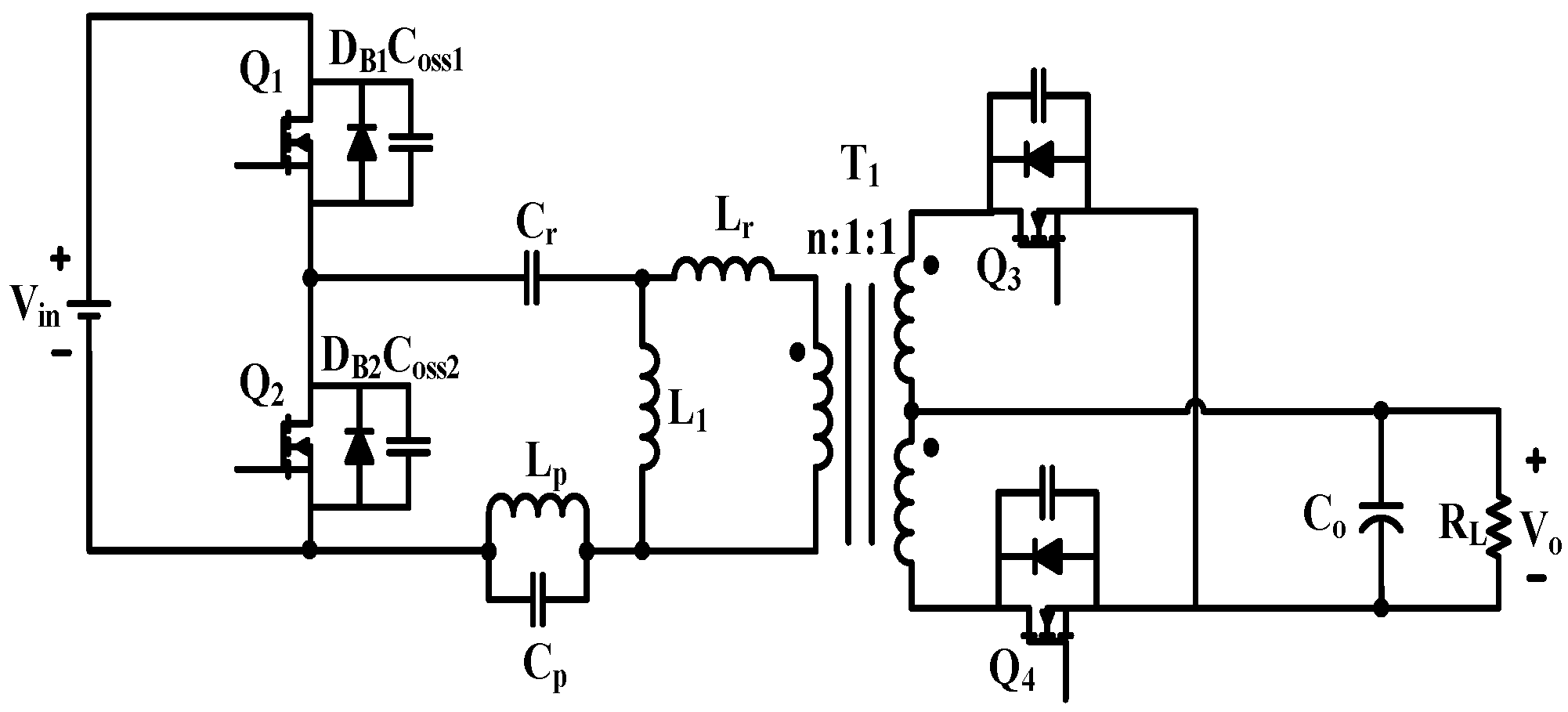
Figure 2.
Key waveforms of the proposed CLL-LC multi-element resonant converter.

Figure 3.
Conduction paths of (a) State 1, (b) State 2, (c) State 3, (d) State 4, for the proposed CLL-LC multi-element resonant during one switching period.
Figure 3.
Conduction paths of (a) State 1, (b) State 2, (c) State 3, (d) State 4, for the proposed CLL-LC multi-element resonant during one switching period.

Figure 4.
The equivalent circuit of CLL-LC multi-element resonant converter.

Figure 5.
Voltage gain curve of the CLL-LC multi-element resonant converter.

Figure 6.
Diagram of the SR control circuit.

Figure 7.
Waveform of ZVS at primary side MOSFETs (a) upper switch Q1 (b) lower switch Q2.
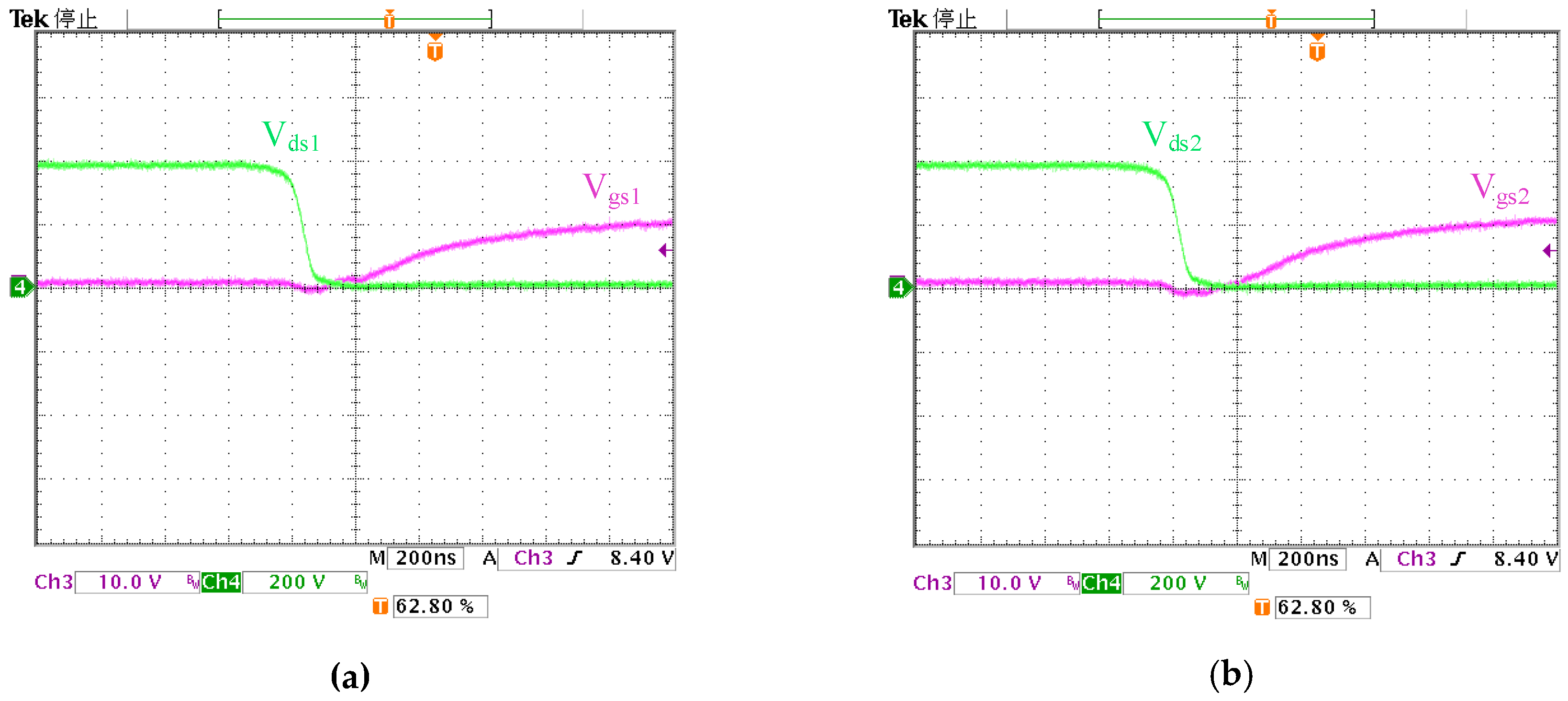
Figure 8.
Waveforms of SRs driving signals Vgs3, Vgs4 and ILrp (a) light load condition (b) full load condition.
Figure 8.
Waveforms of SRs driving signals Vgs3, Vgs4 and ILrp (a) light load condition (b) full load condition.

Figure 9.
Waveforms of inrush current during start-up period (a) conventional LLC resonant converter (b) proposed multi-element CLL-LC resonant converter.
Figure 9.
Waveforms of inrush current during start-up period (a) conventional LLC resonant converter (b) proposed multi-element CLL-LC resonant converter.
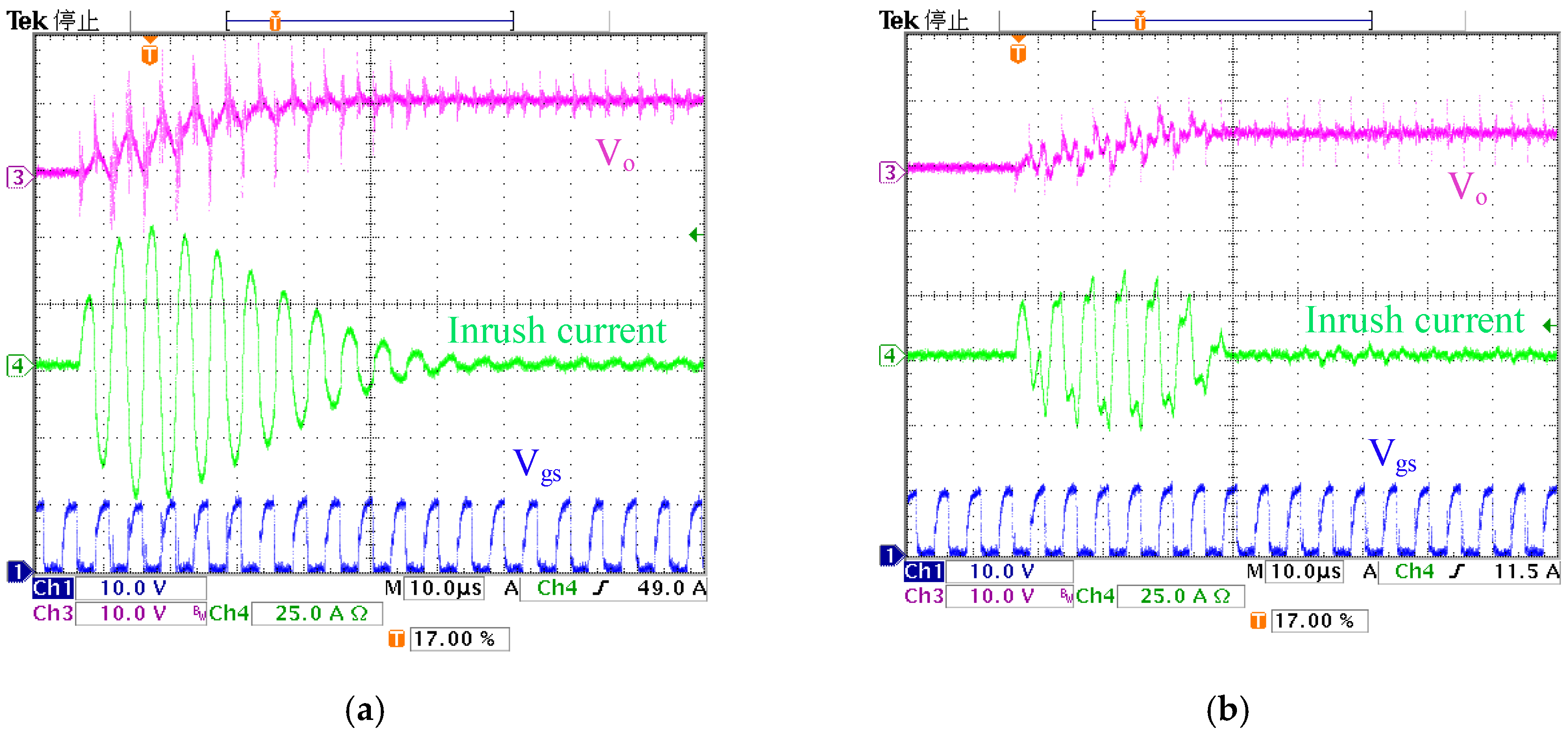
Figure 10.
Efficiency chart of the proposed multi-element resonant converter.

Table 1.
Voltage/Current stress of MOSFETs and resonant element.
| Item | , | , | , , , | |
| Voltage Stress | ||||
| Current Stress (Peak-Current) |
Table 2.
Comparison of LLC and proposed converter.
| Item | LLC Converter | Proposed Converter |
|---|---|---|
| Power device | 4 | 4 |
| Resonant tank elements | 3 | 5 |
| SR detecting circuit | Complex | Simple |
| Over current protect | Difficult | Simple |
| Inrush current | Large | Middle |
| Conversion efficiency | High | High |
Table 3.
Parameters of resonant frequency.
| Resonant frequency fr0 | 15.3 kHz |
| Resonant frequency fr1 | 72.8 kHz |
| Resonant frequency fr2 | 150.2 kHz |
| Resonant frequency fr3 | 225.6 kHz |
© 2019 by the authors. Licensee MDPI, Basel, Switzerland. This article is an open access article distributed under the terms and conditions of the Creative Commons Attribution (CC BY) license (http://creativecommons.org/licenses/by/4.0/).
Share and Cite
MDPI and ACS Style
Lin, J.-Y.; Lin, Y.-F.; Lee, S.-Y. A Novel Multi-Element Resonant Converter with Self-Driven Synchronous Rectification. Energies 2019, 12, 715. https://doi.org/10.3390/en12040715
AMA Style
Lin J-Y, Lin Y-F, Lee S-Y. A Novel Multi-Element Resonant Converter with Self-Driven Synchronous Rectification. Energies. 2019; 12(4):715. https://doi.org/10.3390/en12040715
Chicago/Turabian StyleLin, Jing-Yuan, Yi-Feng Lin, and Sih-Yi Lee. 2019. "A Novel Multi-Element Resonant Converter with Self-Driven Synchronous Rectification" Energies 12, no. 4: 715. https://doi.org/10.3390/en12040715
Note that from the first issue of 2016, this journal uses article numbers instead of page numbers. See further details here.