Article

The Band Structures of Zn1−xMgxO(In) and the Simulation of CdTe Solar Cells with a Zn1−xMgxO(In) Window Layer by SCAPS

1
College of Materials Science and Engineering, Sichuan University, Chengdu 610065, China
2
Chengdu Textile College, Chengdu 611731, China
3
Institute of New Energy and Low-Carbon Technology, Sichuan University, Chengdu 610065, China
4
National Supercomputing Center in Shenzhen, Shenzhen 518055, China
*
Author to whom correspondence should be addressed.
Energies 2019, 12(2), 291; https://doi.org/10.3390/en12020291
Submission received: 9 December 2018 / Revised: 11 January 2019 / Accepted: 15 January 2019 / Published: 18 January 2019

Abstract

:
Wider band-gap window layers can enhance the transmission of sunlight in the short-wavelength region and improve the performance of CdTe solar cells. In this work, we investigated the band structure of In-doped Zn1−xMgxO (ZMO:In) by using first-principles calculations with the GGA + U method and simulated the performance of ZMO:In/CdTe devices using the SCAPS program. The calculation results show that with the increased Mg doping concentration, the band gap of ZMO increases. However, the band gap of ZMO was decreased after In incorporation due to the downwards shifted conduction band. Owing to the improved short circuit current and fill factor, the conversion efficiency of the ZMO:In-based solar cells show better performance as compared with the CdS-based ones. A highest efficiency of 19.63% could be achieved owing to the wider band gap of ZMO:In and the appropriate conduction band offset (CBO) of ~0.23 eV at ZMO:In/CdTe interface when the Mg concentration x approaches 0.0625. Further investigations on thickness suggest an appropriate thickness of ZMO:In (x = 0.0625) in order to obtain better device performance would be 70–100 nm. This work provides a theoretical guidance for designing and fabricating highly efficient CdTe solar cells.

1. Introduction

Cadmium telluride (CdTe) solar cells are some of the most representative thin-film solar cells, characterized by high efficiency and low-cost. CdTe solar cells are widely utilized in power stations, building integrated photovoltaics system (BIPV) and so on [1,2,3]. In recent years, the world record efficiency of CdTe thin-film solar cells has improved significantly, from 17.3% (2011) [4] to 22.1% (2016) [5]. Studies show that this rapid progress has mainly resulted from enhancements in short-circuit current density (Jsc), both in the short and long wavelength regions, by optimizing the window layers [6]. Typically, CdTe solar cells use n-CdS window layer to form heterojunctions [7]. However, CdS is a strong absorber of light with energy lower than its band-gap 2.4 eV. Photons absorbed by the CdS layer will not generate any photocurrent and as a result, poor response to the shortwave solar spectrum (below 510 nm) was witnessed [8].
Wide band-gap semiconductor materials play an important role in the window layer of CdTe solar cells in terms of optimizing the spectral response in the short wavelength range [9]. Mg-substituted ZnO (Zn1−xMgxO) is an important transparent conducting oxide candidate due to its wide band-gap and tunable electron affinity [10]. The band gap in Zn1−xMgxO (ZMO) alloys increases with the increasing concentration of Mg and the conduction band alignment as well as the Fermi-level position in oxide-heterostructures are correlated with the varied concentration [11]. The increased band gap of the top contact offers the potential for improving the ultraviolet (UV) response in solar cells [12]. The Colorado State University (CSU) research group reported that ZMO window layer can essentially eliminate short-wavelength response losses [11]. Minemoto et al. applied ZMO thin films in Cu(In,Ga)Se2 (CIGS) solar cells to replace the conventional CdS and found that the majority carrier recombination via ZMO/CIGS interface defects could be greatly suppressed and good device performances were then obtained with appropriate CBO between ZMO and CIGS device performance could be significantly affected by CBO the device performance [13].
The first-principles approach is an important and pervasive tool to calculate the electronic structure of periodic crystalline materials. SCAPS is a one-dimensional solar cell simulation program. It is a powerful program to model the performance of the solar cells, developed by the Burgelman group of the University of Ghent in Belgium. SCAPS was originally developed for cell structures of the CuInSe2 and the CdTe solar family. Several extensions however have improved its capabilities so that it is also applicable to crystalline solar cells (Si and GsAs family). The basic principle of the program is to solve the Poisson equation and continuity equations of the current under some constraints according to the established device structure model. It was widely used to simulate the device parameters of CIGS [14,15], CZTS [16,17] and CdTe [18,19] solar cells. Most of the simulation results are consistent with the experimental performances and provide important indications for experimental work. Therefore, in this work, we use first principles combined with SCAPS to explore the device performance of CdTe solar cells.
In our previous work [20], we demonstrated higher Jsc in a ZMO window layer than CdS due to its wider band gap than CdTe-based solar cells. Despite of the impressive ZMO/CdTe solar cell improvement compared with CdS/CdTe, it is still only ~18%. We speculated this was mainly caused by a relatively weak diode and insufficient built-in potential between ZMO and CdTe, which was derived from a ZMO window layer with a low doping density about ~1015 cm−3 [21]. Such low-level doping of n-type layers is detrimental to form a high-quality n+-p heterojunction with enough driving force to repel the photogenerated carriers. Furthermore, Ke et al. [22] have reported that a substantial and usually undesired decrease in the maximum obtainable conductivity with increasing Mg content, which limits its practical application as a wider-gap semiconductor. Also, like ZnO itself, ZMO can be degenerately doped n-type by substitutional doping on the cation lattice with Al3+, Ga3+ or In3+ [23,24]. Many studies have shown that doping by these impurity atoms can increase the conductivity of ZMO (to create electronic carriers) [25,26]. Furthermore, the electron affinity and Fermi energy levels of ZMO could also be further modulated [23]. This tunability is very important to optimize the performance of ZMO-based optoelectronic devices. Here, we investigated the electronic structure of In doped ZMO (ZMO:In) by adopting the first-principles calculation with GGA + U method based on the density function theory (DFT). Based on the band structure of ZMO:In, the ZMO:In/CdTe solar cell was simulated by using the SCAPS program. This work may offer a theoretical basis for the n-type doping experiments and the optoelectronic applications of ZMO-based devices.

2. Theoretical Model and Computational Methods

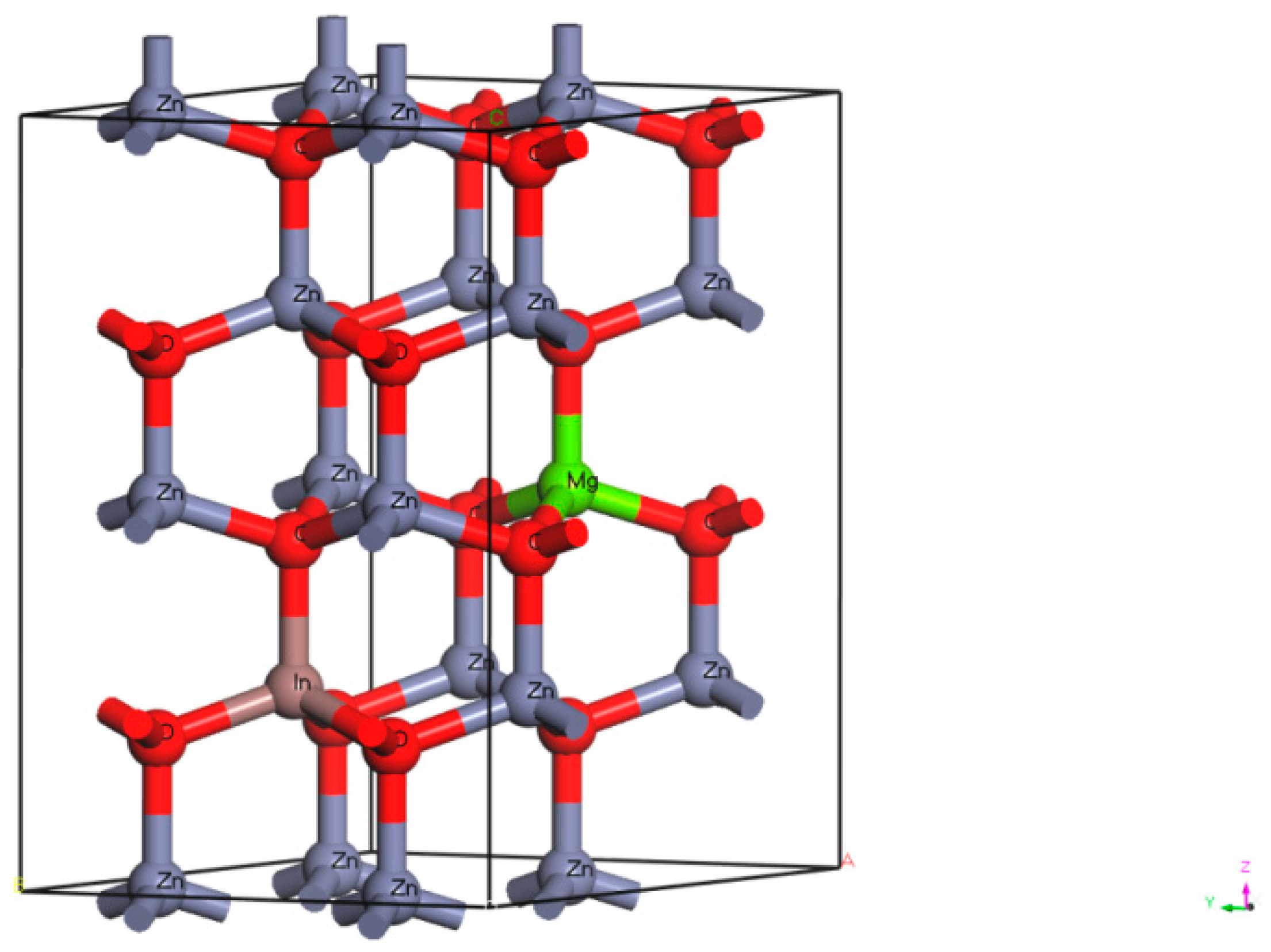
2.1. ZMO:In Model and Computational Method

We consider a 2 × 2 × 2 supercell of a ZnO with wurtzite structure, which contains 32 atoms (16 Zn atoms and 16 O atoms). In order to simulate In-doped ZMO, one of the Zn atoms is substituted with an In atom. The doping concentration of Mg is set as 0, 0.0625, 0.125, 0.1875, 0.25 and the dopant concentration of In is 0.0625. Figure 1 gives the crystal structure of Mg-In co-doped ZnO. It is generally acknowledged that for Al, Ga, In and Mg doped ZnO, substitute doping is the most common type [23,27]. Here, we assumed that two Zn atoms were substituted by one Mg and one In atom, respectively.
Our calculations are carried out by using the Cambridge Serial Total Energy Package (CASTEP) code, which is based on DFT [27], using the ultra-soft-pseudopotentials method. We propose the generalized gradient approximation (GGA) with the introduction of the on-site Coulomb interaction parameter GGA + U method, to investigate the band structure of In doped Zn1−xMgxO (0 ≤ x ≤ 0.25). The U values thus obtained are: Ud,Zn = 10.5 eV and Up,O = 7.0 eV [28]. We use an energy cut-off equals to 480 eV for the plane-wave basis-set expansion. Integrations in the Brillouin zone are performed using k-point sampling on a 4 × 4 × 2 mesh parameter grid. All the structures are fully relaxed and are finished when the total energy and the max force converged to less than 10−6 eV/atom and lower than 0.01 eV/nm, respectively.

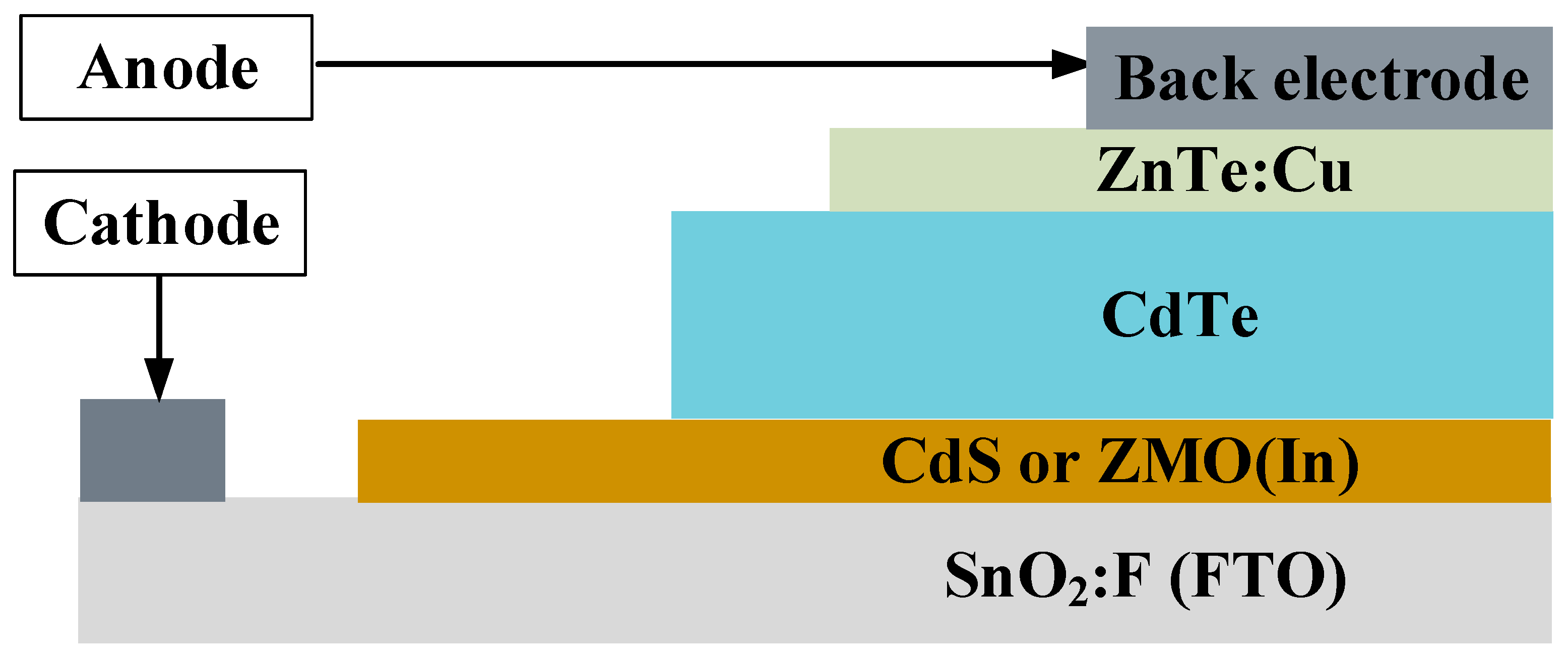
2.2. CdTe Solar Cell Model and Simulation

Figure 2 shows a schematic diagram of a CdTe solar cell with CdS or ZMO:In films as the window layers. The device structure of CdTe solar cells used in the simulation consists of SnO2:F (FTO) layer, CdS or ZMO:In layer, CdTe absorber, back contact (ZnTe: Cu) and metal electrode.
The CdS/CdTe-based structure is used as the baseline and the simulation was conducted with ZMO:In replacing the CdS layer and the input parameters of the other layers kept unchanged, and constrained to the more reasonable ranges of the experimental data for the typical CdTe solar cells. A defect density of 5 × 1016 cm−3 was chosen for the CdS layer [19]. The defect density of 1016 cm−3 was used for the ZMO:In layer for the simulation.
Table 1 summarized all the input parameters. All of the parameters for simulation are all fixed except where otherwise stated. This model is a simplification of the actual cell and ignores any phenomena related to polycrystallinity, such as the loss of surface reflection. Furthermore, the facts that light is absorbed in the transparent conductive film and window layer, and all the incident light passes through to the absorption layer are also neglected. Relevant electric and optical parameters are given in Table 1, and most input parameters for the simulations were mainly collected from relevant theories, the literature [14,19,20,29] or estimated in a reasonable range, etc. Density of at states the conduction band minimum (Nc) and valence band maximum (Nv) are calculated using Equation (1) [14]:
N c / v = 2 ( 2 π m e / p k T h ) 3 / 2
where m e / p are the effective band masses of electrons/holes, h is Planck’s constant and k is the Boltzmann constant. Thermal velocities for electrons (ve)and holes (vp) are obtained from Equation (2) [14]:
v e / p = 3 k T m e / p
We can get the values on the effective electron and hole masses of the ZMO:In layers by the first-principle, and the other layers are drawn from the literature [25,26,30]. The simulated CdS/CdTe solar cell efficiency is close to the results that calculated by using the SCAPS software in [19].

3. Results and discussion

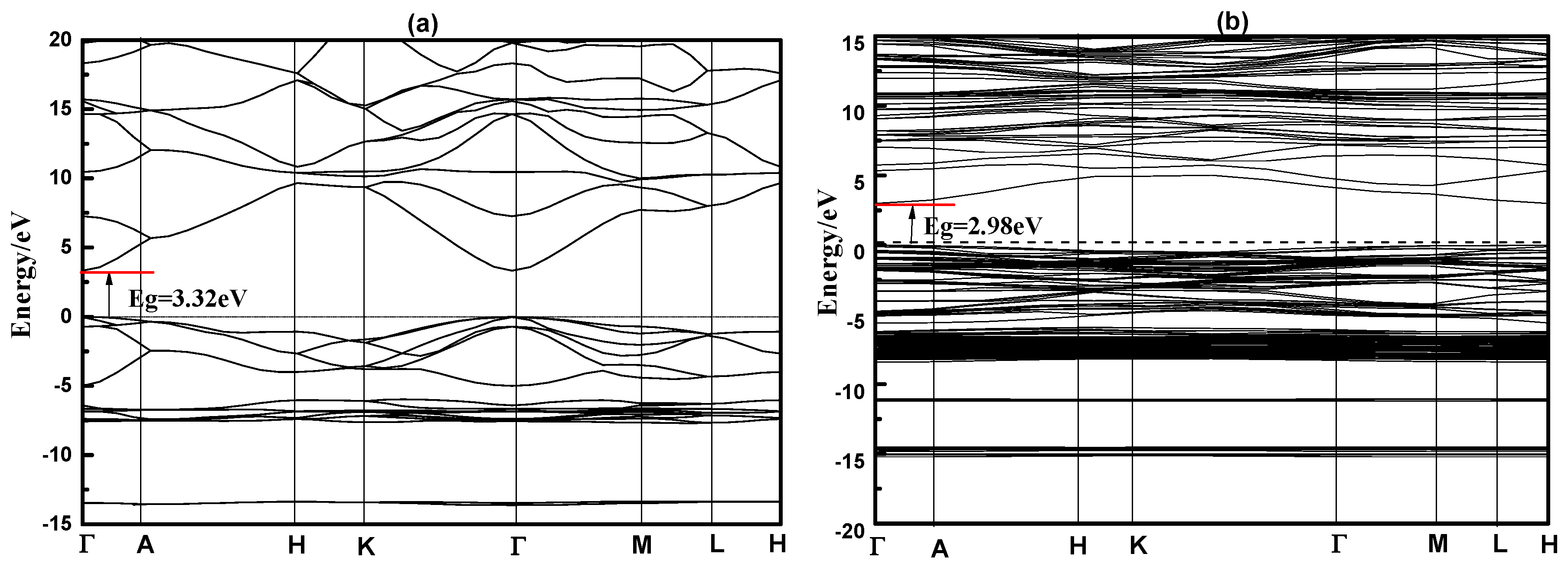
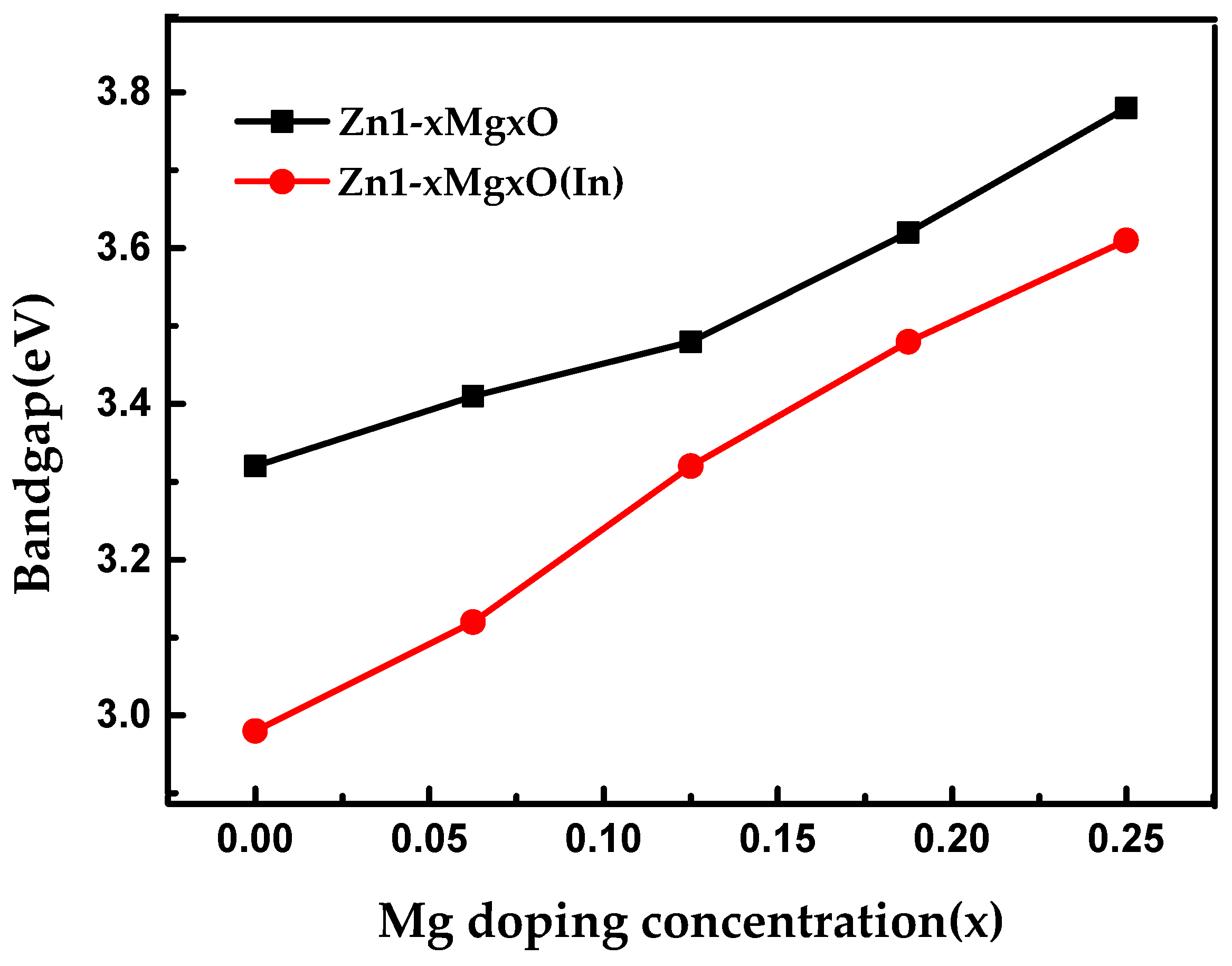
3.1. The Band Structure of ZMO:In

The band structures of ZMO:In (0 ≤ x ≤ 0.25) are calculated by connecting the high-symmetry point in the Brillouin zone. Figure 3 shows the band structures of pure ZnO and In-doped ZnO.
The calculated band structure indicates a direct band gap of ZnO. The corresponding band gap is about 3.32 eV at the highly symmetric Γ point (see Figure 3a), which is close to the experimental value (3.4 eV) [26]. However, the incorporation of In decreases the band gap of ZnO, which is consistent with a previous report [30]. The reason is that conduction band moves to the low-energy region as In atoms are incorporated into ZnO lattice, and as a result, the band-gap becomes narrower.
Figure 4 presents the DOS of ZnO and ZnO:In. It indicates that after In doping, the Fermi level enters the conduction band. Because the energy of In-5p states is lower than that of Zn-4s states, antibonding p, formed by the orbiting electrons between In-5p states and O-2p states, has lower energy than the antibonding s in pure ZnO. Besides, In-5p states and O-2p states tend to the direction of low energy, resulting in the decrease of conduction band. Therefore, Fermi level shift downward into valence band and electrons of Fermi level jumps into the conduction band. As a result, the carrier concentration of system increased. It may be because of the increased free electrons due to the addition of In.
Figure 5 presents the band gaps of Zn1−xMgxO and Zn1−xMgxO:In. The calculated band gap shows a significant increase with the increased concentration of Mg. The band gap of Zn1−xMgxO increases from 3.32 to 3.78 eV with the increase of Mg concentration among different doping cases, which is consistent with [27]. The reason is that with an increased number of Mg atoms in the ZnO lattice, the conduction band moves to the high-energy region and thus its band gap becomes larger than that of pure ZnO. However, the incorporation of In decreases the band-gap of Zn1−xMgxO. The conduction band minimum and the valence band maximum of Zn1−xMgxO:In decrease with In doping. The decrease of conduction band minimum is much more pronounced than that of the valence band maximum, which leads to the reduction of the band gap. Moreover, it was found that the lattice constant will be increased due to In-doping and this also reduces the band gap.

3.2. The Photovoltaic Applications of ZMO:In

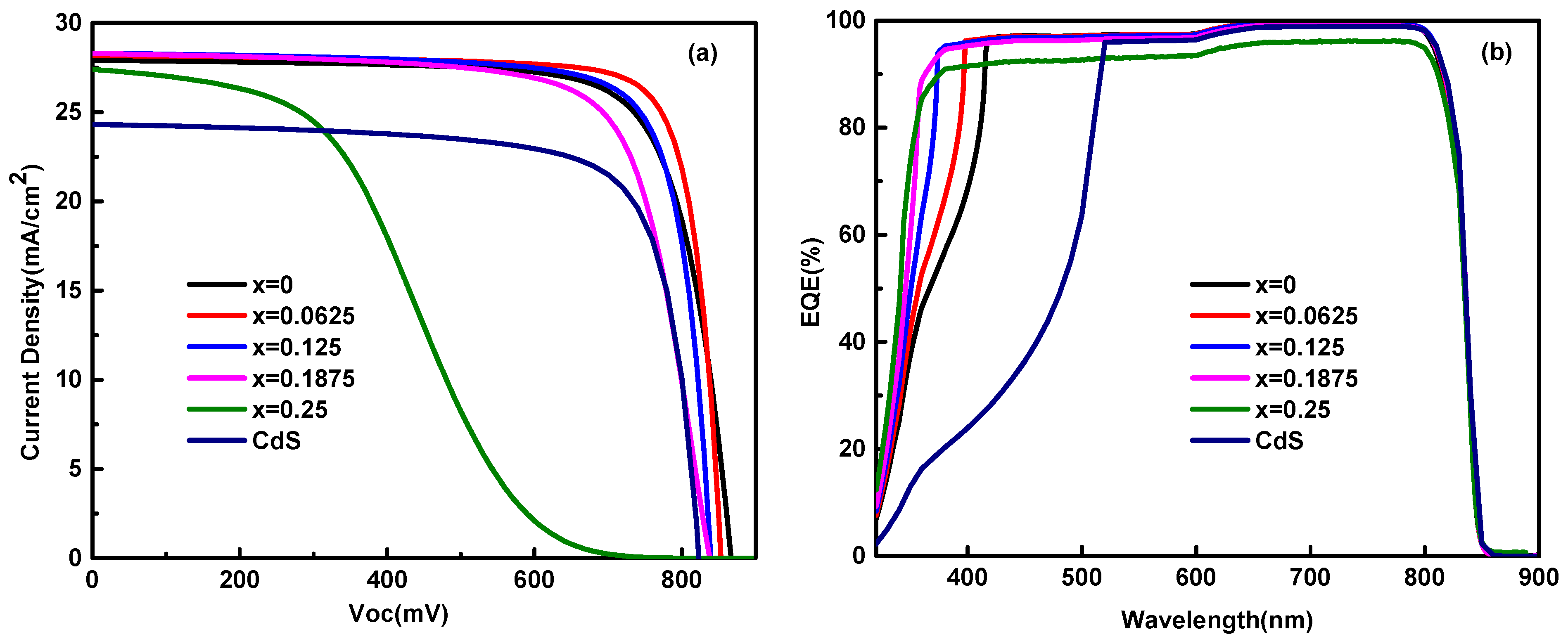
3.2.1. The Performance of CdTe Solar Cells with ZMO:In Window Layers

Figure 6 shows the illuminated current density-voltage and the external quantum efficiency (EQE) for CdS/CdTe and ZMO:In/CdTe solar cells. Here, all SCAPS simulations have been performed under standard illumination conditions: 100 mW/cm2 AM 1.5 spectrum at 300 K. The shunt resistance (Rsh) and series resistance (Rs) were estimated from the J-V curves by fitting the slope of the current density near the short circuit current point and open circuit voltage point, respectively [31,32].
For the baseline model of CdTe solar cells, the cell structure is FTO/CdS/CdTe/ZnTe:Cu/Au. The parameters of each layer are given in Table 1 and the simulated power conversion efficiency of the CdS/CdTe solar cell is 15.06% (Jsc = 24.34 mA/cm2; Voc = 821 mV; FF = 75.18%), which is consistent with the previous report [21]. It is reasonable that the property parameters and defect settings for each layer are close to that in the actual device performance. Table 2 shows that the Jsc of CdTe solar cells increased to the maximum value 28.29 mA/cm2 when the Mg concentration x is 0.125, Although the Jsc (28.16 mA/cm2) is a bit lower than 28.29 mA/cm2 when x is 0.0625, FF reaches its maximum value 81.7%, and the conversion efficiency reaches the maximum 19.63%. One may also notice that, as shown in Table 2, with the increased concentration of Mg from x = 0 to x = 0.1875, the series resistance of device increased from 5.2 Ω·cm2 to 9.6 Ω·cm2. This increase was mainly caused by a substantial decrease in the ZMO conductivity with increasing Mg content [10]. On the contrary, the shunt resistance increased from 1019 Ω·cm2 to 1253 Ω·cm2 with x varied from 0 to 0.0625, followed by a decrease with further increased Mg content. The Rsh declined to 236 Ω·cm2 till x = 0.25. The variation of the Rs and Rsh is consistent with the effect of conduction band offset.
The main contribution of the CdTe efficiency improvement was attributed to the increase of short-circuit current density except for the case that x = 0.0625. Figure 6b shows that the lower quantum efficiency of CdTe solar cell was achieved for the CdS window layer based device, especially in the short wavelength range from 300 nm to 510 nm. The main reason is that CdS has a narrow band gap (2.4 eV), and poor response to the solar shortwave spectrum. For the ZMO:In layers with Mg concentration x increasing 0 to 0.25, a higher EQE was achieved. Obviously, the wide band-gap of ZMO:In films resulted in more photons transmitted into the CdTe film. Consequently, more photogenerated carriers were created in the CdTe film, and thus the short-circuit current density was improved. One may notice that the EQE approaches 100% in the long wavelength region. This is because that this model is a simplification of the actual cell and ignores any phenomena related to polycrystallinity, such as the loss of surface reflection. Furthermore, the light absorption in the transparent conductive film and window layer is also neglected. In this case all the incident light reaches the absorption layer without any loss and the EQE will be exaggerated, but this will not affect the conclusions in the present work. Similar results were also observed in other reports [19].

3.2.2. The Energy Band Alignment of the ZMO:In/CdTe Interface

The photon absorption and separation ability of the device is closely related to the CBO of the window/CdTe layers. The orientation dependence of the energy band alignment at the CdS/CdTe interface was first discovered by Niles and Hochst using synchrotron radiation photoelectron spectroscopy back in 1990 [33]. Their experiments showed a CBO at the CdS/CdTe interface of ΔECB = −0.1 eV, which is ideally suited for high conversion efficiency. Therefore, the fact that CBO values affect the efficiency of solar cells is very crucial.
The improvement of Jsc can be attributed to the suppression of recombination at the ZMO:In/CdTe interface due to the appropriate CBO. In order to further analyse the effects of intrinsic causes and mechanisms on the CdTe device performance, here, we depicted the band diagrams of ZMO:In/CdTe layers, as shown in Figure 7. The band alignment is based on the energy band parameters of ZMO:In, as labelled in Table 3 and CdTe energy band parameters from the literature [11] (χCdTe = 4.5 eV, Eg = 1.5 eV). A spike is formed at the window/CdTe interface due to different electron affinity of the window layer and CdTe layer. A barrier spike (ΔEc) was formed at the ZMO:In/CdTe interface due to different electron affinity (χ) between ZMO:In and CdTe. The specific values of spike (ΔEc) could be obtained from the formula ΔEc = χZMO:In − χCdTe. The barrier spike gradually decreased from 0.27 eV (x = 0) to −0.26 eV (x = 0.25), with Mg concentration x increasing from 0 to 0.25. The results indicate that the conduction band offset of ZMO:In/CdTe layers can be controlled by changing the Mg concentration.
Figure 7a–c show the band diagrams of the CdTe solar cells when the conduction band minimum of the window layers ZMO:In is above that of CdTe. A spike is formed at the ZMO:In/CdTe interface. The Jsc reached 28.16 mA/cm2 due to the appropriate CBO when the spike is about 0.23 eV (x = 0.0625), and the FF reached its peak. As the CBO becomes flat or a cliff, there is both a decreasing device Jsc and FF and increasing loss of current due to interface recombination. As discussed above, Jsc and FF can be improved by adjusting the CBO of window/CdTe layers. If the barrier is too high (ΔEc over 0.23 eV), that will hinder the transport of photogenerated electrons from CdTe to ZMO:In. This will then increase the equivalent series resistance of the CdTe solar cell (corresponding to x < 0.0625). On the contrary, in the case of low barrier spike, it will act as a barrier against the injected electrons from n-type region at forward bias. As a result, the recombination probability of the electrons and holes at the ZMO:In/CdTe interface increases drastically, resulting in a leakage conduction (corresponding to x > 0.125), as shown in Figure 7d,e. Furthermore, series and shunt resistance of the device also affect the performances. The decreased Rs and increased Rsh resulted in an improved FF, that is an optimal value of 81.70% when Mg concentration x = 0.0625.
As discussed above, an appropriate spike is necessary at the window/CdTe interface to depress the majority carrier recombination via the interface defects while not impeding electrons transportation to window layer. When the conduction band minimum of ZMO:In exceeded that of CdTe by more than ~0.23 eV (x = 0.0625), the highest conversion efficiency of 19.63% was achieved. This is significantly optimized as compared with the CdS based one. The improvement of efficiency can be attributed to the suppression of recombination at the ZMO:In/CdTe interface due to an appropriate conduction band offset.

3.2.3. Effect of ZMO:In (x = 0.0625) Thickness on CdTe Solar Cells Performances

To further optimize the window layer, the dependence of the CdTe solar cells on the thickness of ZMO:In (x = 0.0625) film was investigated. We simulated the EQE of CdTe solar cells based on ZMO: In when the thickness varied from 70 nm to 200 nm. Figure 8 gives the simulation results.
Table 4 shows the detailed performance parameters of the champion cells for ZMO:In (x = 0.0625). In this case, the short-circuit current density was decreased with the increase in the thickness of ZMO:In due to the fact Rs increases slightly, while there was no substantial variation of the open-circuit voltage and fill factor. This is because the CBO between ZMO:In and CdTe layers kept unchanged. The results indicate that the window layer absorbs more short-wave photons with increased thickness, which severely deteriorate the photo-electric current. Figure 8 presents that the spectral response in the short wavelength range of 320 nm~400 nm decreases drastically when the ZMO:In thickness is increased to over 100 nm. This is consistent with the performance, especially the Jsc of ZMO:In based solar cells. Furthermore, ZMO:In window layers with the thickness from 70 nm to 100 nm lead to quite similar device performances despite a negligible Jsc loss. This result suggests that the effect of ZMO:In thickness is not significant in the range of <120 nm. Therefore, in the practical device fabrication, good performance could be obtained if the thickness of ZMO:In window layer could be controlled at 70 nm~100 nm.

4. Conclusions

We have investigated the band structure of Mg-In co-doped ZnO based on the density function theory (DFT). It is found that the band gap of Mg-In co-doped ZnO is smaller than that of the ZMO and increases as the content of Mg is increased. Based on the theoretical calculation results of ZMO:In, ZMO:In/CdTe solar cells were modeled using the SCAPS program and the device performances were simulated and analyzed extensively. The results suggest that the optimal conversion efficiency of CdTe solar cell with ZMO:In window layer could be as high as 19.63% when an appropriate CBO of 0.23 eV (Mg content x = 0.0625) was formed at the ZMO:In/CdTe interface. Furthermore, the effect of ZMO:In thickness is mainly on the short-circuit current density of CdTe solar cells. Our insights into the device performance indicate that the performance of CdTe solar cells could be optimized by using a 70–100 nm-thick ZMO:In window layer with dopant concentrations for both Mg and In of 0.0625. These simulation results offer important indications for the design of window layers and provide a theoretical guidance for the fabrication of highly efficient CdTe solar cells.

Author Contributions

Conceptualization, L.W. and J.Z. and L.F.; methodology, L.W.; software, Z.D.; validation, L.W.; formal analysis, X.H. (Xia Hao); writing—original draft preparation, X.H. (Xu He) and X.H. (Xia Hao); Data curation, W.W.; Investigation, X.H. (Xu He) and C.L.

Funding

This research was funded by National Key Research and Development Program of China: Newton Fund-China-UK Research and Innovations Bridges (Grant No. 2016YFE0124500) and the Fundamental Research Funds for the Central Universities (Grant No. YJ201722).

Acknowledgments

The authors acknowledge the use of SCAPS program developed by Burgelman’s group of the University of Ghent, Belgium. In addition, the authors would like to thank National Supercomputing Center in Shenzhen for providing simulation calculation support.

Conflicts of Interest

The authors declare no conflict of interest.

References

  1. Cruz, L.R.; Pinheiro, W.A.; Medeiro, R.A.; Ferreira, C.L.; Dhere, R.G.; Duenow, J.N. Influence of heat treatment and back contact processing on the performance of CdS/CdTe thin film solar cells produced in a CSS in-line system. Vacuum 2013, 87, 45–49. [Google Scholar] [CrossRef]
  2. Kephart, J.M.; Geisthardt, R.M.; Sampath, W.S. Optimization of CdTe thin-film solar cell efficiency using a sputtered, oxygenated CdS window layer. Prog. Photovolt. Res. Appl. 2015, 23, 1484–1492. [Google Scholar] [CrossRef]
  3. Marjani, S.; Khosroabadi, S.; Sabaghi, M.A. High Efficiency Ultrathin CdTe Solar Cell for Nano-Area Applications. Opt. Photonics J. 2016, 6, 15–23. [Google Scholar] [CrossRef]
  4. Paudel, N.R.; Yan, Y. Enhancing the photo-currents of CdTe thin-film solar cells in both short and long wavelength regions. Appl. Phys. Lett. 2014, 105, 606–3911. [Google Scholar] [CrossRef]
  5. Green, M.A.; Hishikawa, Y.; Dunlop, E.D.; Levi, D.H.; Hohl-Ebinger, J.; Yoshita, M.; Ho-Baillie, A.W. Solar cell efficiency tables (Version 53). Prog. Photovolt. Res. Appl. 2018, 27, 3–12. [Google Scholar] [CrossRef]
  6. Korevaar, B.A.; Cournoyer, J.R.; Sulima, O.; Yakimov, A.; Johnson, J.N. Role of oxygen during CdTe growth for CdTe photovoltaic devices. Prog. Photovolt. Res. Appl. 2015, 22, 1040–1049. [Google Scholar] [CrossRef]
  7. Colegrove, E.; Blissett, C.; Buurma, C.; Ellsworth, J.; Morley, M. High-Efficiency Polycrystalline CdS/CdTe Solar Cells on Buffered Commercial TCO-Coated Glass. J. Electron. Mater. 2012, 41, 2833–2837. [Google Scholar] [CrossRef]
  8. Martin, A.; Emery, K. Solar cell efficiency tables (version 42). Prog. Photovolt. Res. Appl. 2013, 21, 827–837. [Google Scholar] [Green Version]
  9. Peelaers, H.; Kioupakis, E.; Van de Walle, C.G. Fundamental limits on optical transparency of transparent conducting oxides: Free-carrier absorption in SnO2. Appl. Phys. Lett. 2012, 100, 011914. [Google Scholar] [CrossRef]
  10. Yi, K.; Lany, S.; Berry, J.J.; Perkins, J.D.; Parilla, P.A. Enhanced Electron Mobility Due to Dopant-Defect Pairing in Conductive ZnMgO. Adv. Funct. Mater. 2014, 24, 2875–2882. [Google Scholar]
  11. Kephart, J.M.; McCamy, J.W.; Ma, Z.; Ganjoo, A.; Alamgir, F.M.; Sampath, W.S. Band alignment of front contact layers for high-efficiency CdTe solar cells. Sol. Energy Mater. Sol. Cells 2016, 157, 266–275. [Google Scholar] [CrossRef] [Green Version]
  12. He, X.; Song, Y.H.; Wu, L.L.; Li, C.X.; Zhang, J.Q.; Feng, L.H. Simulation of high-efficiency CdTe solar cells with Zn1−xMgxO window layer by SCAPS software. Mater. Res. Express 2018, 5, 065907. [Google Scholar] [CrossRef]
  13. Minemoto, T.; Hashimoto, Y.; Satoh, T.; Negami, T.; Takakura, H.; Hamakawa, Y. Cu(In,Ga)Se2 solar cells with controlled conduction band offset of window/Cu(In,Ga)Se2 layers. J. Appl. Phys. 2001, 89, 8327–8330. [Google Scholar] [CrossRef]
  14. Pettersson, J.; Platzer, B.; Rkman, C.; Zimmermann, U. Baseline model of graded-absorber Cu(In,Ga)Se2 solar cells applied to cells with Zn1−xMgxO buffer layers. Thin Solid Films 2011, 519, 7476–7480. [Google Scholar] [CrossRef]
  15. Minemoto, T.; Matsui, T.; Takakura, H.; Hamakawa, Y.; Negami, T.; Hashimoto, Y.; Uenoyama, T.; Kitagawa, M. Theoretical analysis of the effect of conduction band offset of window/CIS layers on performance of CIS solar cells using device simulation. Sol. Energy Mater. Sol. Cells 2001, 67, 83–88. [Google Scholar] [CrossRef]
  16. Patel, M.; Ray, A. Enhancement of output performance of Cu2ZnSnS4 thin film solar cells—A numerical simulation approach and comparison to experiments. Phys. B Condens. Matter 2012, 407, 4391–4397. [Google Scholar] [CrossRef]
  17. Olopade, M.A.; Oyebola, O.O.; Adeleke, B.S. Investigation of some materials as buffer layer in copper zinc tin sulphide (Cu2ZnSnS4) solar cells by SCAPS-1D. Adv. Appl. Sci. Res. 2012, 3, 3396–3400. [Google Scholar]
  18. Clayton, A.J.; Carlo, V.D.; Irvine, S.J.C. Investigation into ultrathin CdTe solar cell Voc using SCAPS modelling. Mater. Res. Innov. 2014, 18, 505–508. [Google Scholar] [CrossRef] [Green Version]
  19. Huang, C.H.; Chuang, W.J. Dependence of performance parameters of CdTe solar cells on semiconductor properties studied by using SCAPS-1D. Vacuum 2015, 118, 32–37. [Google Scholar] [CrossRef]
  20. He, X.; Ren, S.Q.; Li, C.X.; Wu, L.L.; Zhang, J.Q.; Du, Z. Zn1−xMgxO: Band Structure and Simulation as Window Layer for CdTe Solar Cell by SCAPS Software. J. Inorg. Mater. 2018, 33, 635–640. [Google Scholar]
  21. Wang, T.; Ren, S.; Li, C.; Li, W.; Liu, C.; Zhang, J.; Wu, L.; Li, B.; Zeng, G. Exploring window buffer layer technology to enhance CdTe solar cell performance. Sol. Energy 2018, 164, 180–186. [Google Scholar] [CrossRef]
  22. Ke, Y.; Berry, J.; Parilla, P.; Zakutayev, A.; O’Hayre, R.; Ginley, D. The origin of electrical property deterioration with increasing Mg concentration in ZnMgO:Ga. Thin Solid Films 2012, 520, 3697–3702. [Google Scholar] [CrossRef]
  23. Matsubara, K.; Tampo, H.; Shibata, H.; Yamada, A.; Fons, P.; Iwata, K.; Niki, S. Band-gap modified Al-doped Zn1−xMgxO transparent conducting films deposited by pulsed laser deposition. Appl. Phys. Lett. 2004, 85, 1374–1376. [Google Scholar] [CrossRef]
  24. Senthil, T.S.; Muthukumarasamy, N.; Kang, M. Improved performance of ZnO thin film solar cells by doping magnesium ions. J. Mater. Sci. Mater. Electron. 2013, 24, 3963–3969. [Google Scholar] [CrossRef]
  25. Zhu, Y.Z.; Chen, G.D.; Ye, H. Electronic Structure and Phase Stability of MgO, ZnO, CdO, and Related Ternary Alloys. Phys. Rev. B 2008, 77, 245209. [Google Scholar] [CrossRef]
  26. Tampo, H.; Yamada, A.; Fons, P. Degenerate layers in epitaxial ZnO films grown on sapphire substrates. Appl. Phys. Lett. 2004, 84, 4412–4414. [Google Scholar] [CrossRef]
  27. Si, X.; Liu, Y.; Lei, W. First-principles investigation on the optoelectronic performance of Mg doped and Mg–Al co-doped ZnO. Mater. Des. 2016, 93, 128–132. [Google Scholar] [CrossRef]
  28. Sheetz, R.M.; Ponomareva, I.; Richter, E.; Andriotis, A.N.; Menon, M. Defect-induced optical absorption in the visible range in ZnO nanowires. Phys. Rev. B Condens. Matter 2009, 80, 195314. [Google Scholar] [CrossRef]
  29. Zhang, J.Q. Study on CdTe and Related Compound Polycrystalline Thin Films as well as CdTe Solar Cell. Ph.D. Thesis, Sichuan University, Chengdu, China, 2002. [Google Scholar]
  30. Paul, B.; Singh, B.; Ghosh, S.; Roy, A. A comparative study on electrical and optical properties of group III (Al, Ga, In) doped ZnO. Thin Solid Film 2016, 603, 21–28. [Google Scholar] [CrossRef]
  31. Han, J.F.; Spanheimer, C.; Haindl, G.; Fu, G.H.; Krishnakumar, V. Optimized chemical bath deposited CdS layers for the improvement of CdTe solar cells. Sol. Energy Mater. Sol. Cells 2011, 95, 816–820. [Google Scholar] [CrossRef]
  32. Ichikawa, M.; Suto, E.; Jeon, H.G. Sensitization of organic photovoltaic cells based on interlayer excitation energy transfer. Org. Electron. 2010, 11, 700–704. [Google Scholar] [CrossRef] [Green Version]
  33. Niles, D.W.; Hartmut, H. Band offsets and interfacial properties of cubic CdS grown by molecular-beam epitaxy on CdTe(110). Phys. Rev. B Condens. Matter 1990, 41, 12710–12719. [Google Scholar] [CrossRef] [PubMed]
Figure 1. Crystal structure of ZnO super cell and doping position.
Energies 12 00291 g001
Figure 2. Device structure of CdTe solar cell for the device simulations.
Energies 12 00291 g002
Figure 3. Calculated band structures of (a) pure ZnO and (b) ZnO:In.
Energies 12 00291 g003
Figure 4. The DOS of ZnO (a) and ZnO:In (b).
Energies 12 00291 g004
Figure 5. The band gap of Zn1−xMgXO and Zn1−xMgXO(In).
Energies 12 00291 g005
Figure 6. (a) J-V curves and (b) external quantum efficiency of CdTe solar cell.
Energies 12 00291 g006
Figure 7. Schematic energy band diagram of ZMO:In/CdTe Layers. (a) x = 0; (b) x = 0.0625; (c) x = 0.125; (d) x = 0.1875 and (e) x = 0.25.
Energies 12 00291 g007
Figure 8. Thickness dependence of external quantum efficiency of CdTe solar cells on ZMO:In (x = 0.0625) film.
Energies 12 00291 g008
Table 1. Simulation parameters for the models of CdS/CdTe and ZMO:In/CdTe solar cells using SCAPS.
Layer ParametersFTO [19]CdS [14,19,29]Zn1−xMgxO(In) [20,29]CdTe [29]ZnTe:Cu [29]
x = 0x = 0.0625x = 0.125x = 0.1875x = 0.25
Eg/eV3.62.42.983.123.323.483.611.452.26
ε/ε08.9910101010101010.1
Nc/cm−35.2 × 10182.2 × 10185 × 10189 × 10171 × 10179 × 10161 × 10169.2 × 10171.5 × 1018
Nv/cm−31.0 × 10191.8 × 10199 × 10189 × 10181 × 10189 × 10171 × 10175.2 × 10181.16 × 1019
Ve/cm.s−11.0 × 1073.1 × 1072.4 × 1072 × 1072 × 1072 × 1072 × 1071 × 1071 × 107
Vp/cm.s−11.0 × 1071.6 × 1071.3 × 1071 × 1071 × 1071 × 1071 × 1071 × 1071 × 107
μn/cm2.v−1.s−1100340100100100100100400400
μp/cm2.v−1.s−1255050505050506050
Carrier density/cm−3n = 1 × 10²⁰n = 1 × 10¹⁷n = 5 × 10¹⁷n = 9 × 10¹⁶n = 1 × 10¹⁶n = 9 × 10¹⁵n = 1 × 10¹⁵p = 1.5 × 10¹⁴p = 1.5 × 10²⁰
Thickness/nm350707070707070500070
ε/ε0: relative permittivity; Nc: effective density of states in conduction band; Nv: effective density of states in valance band; Ve: recombination velocity of electrons; Vp: recombination velocity of holes; μn: electron mobility; μp: hole mobility; n: effective carrier concentration of n-type semiconductor layers; p: effective carrier concentration of p-typed semiconductor layers.
Table 2. The performances of ZMO:In/CdTe solar cells.
ParametersCdSZn1−xMgxO:In (x Represents Mg Concentration)
x = 0x = 0.0625x = 0.125x = 0.1875x = 0.25
Voc (mV)821866853839837858
Jsc (mA·cm−2)24.3427.8928.1628.2928.2727.39
FF (%)75.1876.2281.7078.8473.1732.81
H (%)15.0618.4319.6318.7217.337.72
Rs (Ω·cm2)4.65.26.87.99.625.8
Rsh (Ω·cm2)812101912531156971236
Table 3. The energy band structure parameters of Zn1−xMgxO:In with different Mg concentration x.
x00.06250.1250.18750.25
Eg (eV)2.983.123.323.483.61
Ef (eV)2.482.512.762.892.97
χ (eV)4.774.734.534.374.24
Φ (eV)5.375.345.094.964.88
Table 4. Dependence of CdTe solar cell performance parameters on thickness of ZMO:In (x = 0.0625).
Thickness (nm)70100120150200
Voc (mV)853853853852852
Jsc (mA·cm−2)28.1628.0327.9627.8827.78
FF (%)81.7181.7181.7181.7181.70
η (%)19.6319.5419.4919.4319.35
Rs (Ω·cm2)6.86.96.97.17.3
Rsh (Ω·cm2)12531208117910931025

