Bidirectional Twisted Single-Stage Single-Phase Buck-Boost DC-AC Converter
by
 , ,
, ,
Oleksandr Husev
1,2,*, 
Oleksandr Matiushkin
1,2,
Carlos Roncero-Clemente
3,
Dmitri Vinnikov
1 and 
Vasyl Chopyk
4 1
Department of Electrical Power Engineering and Mechatronics, Tallinn University of Technology (TalTech), 10111 Tallinn, Estonia
2
Biomedical Radioelectronic Apparatus and Systems Department, Chernihiv National University of Technology (ChNTU), 14039 Chernihiv, Ukraine
3
Department of Electrical, Electronic and Control Engineering, School of Industrial Engineering, University of Extremadura, 06006 Badajoz, Spain
4
Institute of Electrodynamics, National Academy of science of Ukraine, 01030 Volodymyrska, Ukraine
*
Author to whom correspondence should be addressed.
Energies 2019, 12(18), 3505; https://doi.org/10.3390/en12183505
Submission received: 12 August 2019
/
Revised: 2 September 2019
/
Accepted: 8 September 2019
/
Published: 11 September 2019
(This article belongs to the Special Issue Emerging DC/AC Converters for Storage and Renewable Application)
Abstract
:This paper describes a bidirectional twisted single-phase single-stage buck-boost dc-ac converter based on an output unfolding circuit. This solution is derived by the combination of an inverting buck-boost dc-dc converter and an unfolding circuit. The operation principle, component design guidelines, along with the control approach are presented. The zero-crossing distortion problem is discussed and solved by a simple approach. The simulation and experimental results confirm all theoretical statements. Loss distribution and achievable efficiency are analyzed. Finally, the pros and cons of the proposed solution, along with the most promising application field, are analyzed and discussed in the conclusion.
1. Introduction
Renewable energy sources require advanced technologies. A photovoltaic (PV) system stands out among the present and future energy systems. The concept of a near zero energy building requires the presence of additional storage elements, which raises the cost of the overall system.
A solar inverter, as part of the PV system, contributes substantially to the overall price and efficiency of the system. System optimization, in terms of price, efficiency, input voltage range operation, and power density, is the priority task in power electronics research. The Google Little Box Challenge (GLBC) demonstrated a close relation with the topic of high-power density inverters for PV applications [1,2,3]. The main GLBC project outcome is the concept of a very high-power density converter. The finalists demonstrated that a basic full-bridge interleaved inverter with an active decoupling circuit, along with wide band-gap semiconductors utilization, may give the best result in terms of power density. At the same time, the mass production market demands simple and cheap solutions. Usually, power density optimization is not a first level priority.
In PV systems, several configurations can be used [4,5]. Single PV panels are available for low power applications. A partial shadowing in the serial or string connection leads to a significant voltage drop, which in turns leads to a wide range of input voltage variations during the energy utilization time. An intermediate voltage boost dc-dc converter can be used to overcome this drawback. It is shown in Figure 1a.
Another application field of the dc-ac converter with wide input voltage regulation is battery storage. Lithium-ion batteries are targeted to become the most popular choice for on-grid and grid-off solar battery storage in the foreseeable future. Such types of batteries have a wide range of input voltage. A converter that accepts different storage elements is preferable.
Several single-stage alternatives were presented as alternative solutions. Inverters with an active boost cell were described in [6,7,8,9]. These inverters provide very high boost of the input voltage but suffer from high current spikes in the semiconductors and passive elements. Impedance-source networks have been reported in many research papers as a promising single-stage solution. Z-source inverters (ZSIs) and quasi-Z-source inverters (qZSIs) were proposed for different applications. Existing solutions were reviewed in [10,11,12,13,14], and different relevant issues are addressed in [15,16,17,18,19,20]. However, recent research revealed evident drawbacks of the IS-based converters in terms of power density and efficiency [21,22,23].
Split-source inverters (SPIs) [24,25] were proposed as another alternative solution. According to the literature, SPIs have less passive component counts accompanied by higher voltage and current stresses at lower voltage gains, and they do not have short circuit immunity.
Several interesting single-stage buck-boost inverters were proposed in [26,27,28,29]. At the same time all of them did not find industrial application. For example, the solution [26] requires reverse-blocking IGBTs, while others are quite complex solutions.
An Aalborg inverter (Figure 1b) is proposed as an inverter that combines buck and boost functionality [30,31,32,33,34,35]. These solutions have two independent buck-boost stages that are responsible for output sinusoidal voltage generation. The main advantage of the proposed solution is in the minimum voltage drop of the filtering inductors in the power loop at any time. At the same time, this solution uses a double number of semiconductors and an inductor in the buck and boost stage, which is an obvious drawback. Another drawback consists in the two power sources utilization. A similar idea with double components is discussed in [36].
The solution based on the input boost and buck converter along with a line frequency unfolding circuit was proposed in [37,38]. The input voltage is boosting to the constant dc-link voltage. The Buck stage performs further modulation, which is unfolding to the sinusoidal voltage.
A modified solution based on the inverting buck-boost dc-dc converter that allows reducing count of inductors is proposed in [39,40]. This paper discusses a grid-connected application of the proposed above discussed solution along with its bidirectional application which extends its application. The objective includes designing a closed-loop control along passive component design with efficiency estimation.
2. Control System of Twisted Single-Phase Single-Stage Inverter based on Unfolding Circuit
The discussed single-phase single-stage buck-boost dc-ac converter based on the unfolding circuit is depicted in Figure 2. This circuit consists of inductances L1, L2 capacitors C1 and C2, switches S1, S2, and low frequency switches T1–T4. The switch S2 can be replaced by a diode D1 in the case of unidirectional operation.
According to the classical definition of the unfolding circuit, transistors T1–T4 realize a simple unfolding circuit. However, these switches can also be used for high frequency modulation.
The proposed solution is derived from the conventional buck-boost dc-dc converter that has a following gain factor B:
where D represents the duty cycle of the switch S1. Taking into account the instantaneous reference output voltage vc2(t), the instantaneous value of the duty cycle D(t) can be expressed as follows:
Figure 3a shows a general control system approach along with the modulation technique. It should be mentioned that the main task of a high-level control system depends on the particular application. Using an output current as a feedback signal, the modulation signal VMOD can be derived by different control approaches including a resonant controller, DQ control, model predictive control, etc. A well-known Second Order Generalized Integrator (SOGI) phase-locked loop (PLL) algorithm for grid synchronization is used in [41].
The duty cycle modulator defines the duty cycle value according to Equation (2). This value defines the switching signal of the transistor S1 by means of a very simple modulation technique. The unfolder’s transistors are controlled by a simple comparison of the capacitor voltage with the zero level.
The modulation signal VMOD is derived from the output current controller. In this case, a simple proportional-resonant (PR) controller with Harmonic Compensation (HC) was used. The control system tuning is based on the transfer function of the proposed solution, which is derived from a small signal model [42]. The transfer function is shown in Figure 3b.
The PR-controller factors were determined based on the transfer function, which takes into account the input stress as the changing of the duty cycle:
The small signal designing is a suitable approach for explaining the topology by analytic expressions. The equivalent circuits include the parasitic resistance of each passive element (Figure 4). These parasitic parts include resistors of on-state semiconductor switches. The presence of three passive elements leads to polynomials with third order in the denominator:
where is a reverse value of the duty cycle, and each parasitic resistance is replaced by .
The tuning approach described in many research papers does not contain any novelty. Reference current IREF can be derived from a high-level algorithm that depends on a particular application, which is out of scope of this paper. If the power flows from the dc to the ac side, it can be derived from the high-level maximum power point tracking algorithm or the battery discharging algorithm. In an opposite power flow, it can be derived by the battery charging algorithm or an additional capacitor voltage vc2 control loop.
3. Component Design Guidelines for Bidirectional Operation
This section describes guidelines for the design of passive and active components taking into account predefined parameters and target losses level in the system.
The main approach of passive element design has relevance to the steady-state analysis. Each period occurs with the processing of energy storage by the input inductance (Figure 4a) and is immediately transferred to the load (Figure 4b). It should be noted that the parasitic parameters are not taken into account in the calculation.
As a rule, the expression of the pulsations of the output capacitor voltage depends on the capacitor current, the switching frequency, and the value of the capacitance. However, the change of the output current depends directly on the ac-part of the capacitor voltage. The area of the capacitor voltage ac-part is proportional to the ripples of the output current.
The values of passive components are expressed as:
where is a current phase of the grid voltage, VM is the amplitude of the grid voltage and KL, KC, Kg are coefficients of corresponding element ripple. The ripples of elements are defined as follows:
The obtained expressions show the dependence between the optimal values of the passive components and the phase of the grid voltage. Also, the high-switching side of the topology allows obtaining a current with only positive values.
Figure 5 shows the influences of the passive component values on the ratio between the input stress and the amplitude of the grid voltage (Equation (9)) at constant input power and input current.
The ripple factor is constant for each element. All the values of inductances or the capacitor are normalized to their value at a point when the input voltage equals the grid voltage maximum:
where L0, Lg0, C0 represent values of the passive elements when the ratio VINp.u. is equal to one unit.
To select a semiconductor, the losses model of the proposed solution is proposed and analyzed. The switching and conduction losses of the MOSFET transistors are taken into account [43]. The conduction losses model is illustrated in Figure 4—it includes the drain-source resistance Rds of transistors, the equivalent series resistance Resr of capacitors and voltage drop on the diode Vfd.
Figure 6 demonstrates the power losses of the topology as the function of the power and the input voltage.
The switching losses at the constant input current and the constant input power are shown in Figure 6b. Figure 6c shows the overall expected efficiency of the converter as a function of the input voltage. In this case, different distributions between the conduction and the switching losses are considered. In the first case (dotted line), semiconductors with a good static characteristic are considered, while in the second case, the conduction losses dominate. The main idea of this quality analysis is to show the possibility of the maximum efficiency point tuning and optimization.
As a conclusion of this section, the values of the passive elements determine the pulsations of current in transistors. The proper selection of the passive components can avoid discontinues current mode, that could lead to unstable behavior. At the same time, the selected topology does not have a dc-link stage, thus no dc-link electrolytic capacitors are required.
4. Simulation Verification of Bidirectional Operation Capability
To verify the theoretical statements and basic operation modes, simulations were performed for proposed solutions in PSCAD simulation tool (Figure 7 and Figure 8). Since the PV or different storage batteries are considered as possible application scenario, a wide range of the input voltage is defined. The values of passive components are illustrated in Table 1.
Figure 7 shows the simulation diagrams for low input voltage and low input power operation mode. Figure 7a shows the rectifier mode, while Figure 7b shows the inverter mode. An ideal sinusoidal grid is considered. In the inverting operation, the average dc input voltage is equal to 250 V, while RMS output voltage is equal to 230 V, and input power is about 250 W. It can be seen that the input current has a continuous mode which is achieved by means of a simple input capacitor.
At the same time, its value is relatively small. In the reverse operation, the sign of reference PR controller current is changed, while the control structure remains the same.
Figure 8 demonstrates very similar simulation results for an increased input voltage (350 V) and power (850 W).
The main outcome from these figures is that simulation results correspond to the theoretical expectation. A very simple control system can provide bidirectional operation with acceptable grid current quality.
5. Experimental Verification
Figure 9 shows the experimental setup for the studied solution. It consists of an inverter PCB board, a control board and an inductor. The passive elements correspond to the simulation study.
The high switching transistors S1, S2 are realized on the MOSFET SiC transistor C2M0080120D along with SiC diode D1 C3D10012A. The diode was used as an alternative solution for unidirectional operation. The unfolding circuit is based on the MOSFET transistors IPB60R060P7ATMA1. These transistors have the poor dynamic characteristics but low static losses.
All the diagrams were derived by current probes Tektronix TCP0150, and voltage probes Tektronix TPA-BNC along with the digital oscilloscope Tektronix MDO4034B-3. A general approach to the experimental verification is shown in Figure 4. A high performance power analyzer YOKOGAVA WT1800 was used for efficiency measurement.
The control system is based on a digital signal processing (DSP) controller and a low-cost field-programmable gate array (FPGA). External ADC converters were implemented to provide high accuracy. This approach is justified by the very high switching frequency of the transistors and the high-level demand of the calculation resources. As a result, the functionality is detached between the FPGA and the DSP. This test bench allows the realization of any PWM technique with a high switching frequency and high resolution. At all operation points, the switching frequency was 60 kHz.
Our experimental study was targeted to achieve several aims. First, the aim was to analyze the influence of the separate control of high switching and unfolding transistors on the zero crossing distortion. Second, the focus was on the influence of synchronous switching of transistors S1 and S2 on the zero crossing distortion. Finally, a detailed efficiency study was conducted.
Figure 10 shows the experimental results at low input voltage Vin = 250 V, and at low power Pin = 250 W in the inverter mode. In this case, several scenarios were tested. The first scenario (Figure 10a) corresponds to the case without synchronous switching of transistors S1 and S2 and without separate control of the unfolding transistors.
Figure 10a shows the output voltage in the grid-off mode, vab voltage before unfolding circuit, inductor iL and input iIN currents. As can be seen, zero crossing distortion is present. Figure 10b shows the same diagrams without synchronous switching of transistors S1 and S2 but with separate control; zero crossing distortion is slightly reduced but not completely eliminated.
Finally, the influence of synchronous switching was estimated. Figure 10c shows that an ideal output voltage shape is achievable in this case. It is explained by an additional discharge circuit that helps to keep the output voltage across the unfolding capacitor very close to sinusoidal shape. The THD value was estimated for all cases and confirms that the last case corresponds to the lowest value <1%.
Similar experimental results are shown in Figure 11 with increased output current. First of all, it should be underlined that an increase in power leads to a decrease in distortion, even in the worst case. Both of these figures show the open loop operation with a simple passive load.
To confirm the grid-connection operation capability, Figure 12 shows the diagrams in the grid-connected mode. It can be seen that despite current distortion, the experimental results are very similar to the simulation results. Slight distortion is caused by non-ideal laboratory grid voltage that can be improved by more sophisticated control, which is beyond the scope of this work. In this working point, THD values in all cases were less than 1%.
6. Efficiency Estimation
The efficiency profile as the function of the input power with constant input voltage is shown in Figure 13a. The open loop unidirectional mode was utilized when the transistor S2 was replaced by a diode.
It can be seen that the characteristic has the peak value of efficiency at about 95%. The point of maximum efficiency is different at different input voltages. The solid line corresponds to 250 V, while the split line corresponds to the input voltage of 350 V. At a lower input voltage, the peak efficiency belongs to the input power of 300 W. At an increased input voltage, the maximum efficiency can be achieved with an increased input power as well.
At the same time, Figure 13b shows the dependence of the efficiency as the function of the input voltage with constant power. The power was investigated in a range from 100 W to 1000 W. The two cases are shown. In the first case, the reduced input power is 250 W. It can be seen that the peak efficiency occurs at a relatively low input voltage. A further increase in the input voltage in the constant power mode will lead to the overall efficiency decreasing. In the second case, illustrated by a split line, the power was increased to 850 W. In this case, the peak efficiency point is evidently shifted to the higher voltage.
The main conclusion is that the converter has some optimal operation point that depends on the input voltage and power level. This conclusion correlates with the theoretical losses model described above. The overall efficiency mostly depends on the conduction losses in the high-switching semiconductors and unfolding transistors. At the same time, it can be optimized for a certain operation point by means of selecting different semiconductors for high switching and unfolding circuit.
Figure 14 shows the next set of experimental tests devoted to the efficiency study in the bidirectional operation mode.
In this case, the diode was replaced by the transistor S2. The diagrams in Figure 14 are similar to those in Figure 13. It can be seen that the efficiency profile behaves very similar to the unidirectional mode. The main difference lies in the significant efficiency increase, which in turn, is explained by the reduction of conduction losses. The maximum 96.2% efficiency is observed in this case.
Figure 15 shows pictures from the thermal camera. In the first case (Figure 15a,b) the input voltage and power were reduced, the total efficiency was about 96%. In the second case, the input power increases along with the input voltage. Figure 15c,d shows the corresponding thermal picture. The efficiency in this case was about 95%. Due to the lower efficiency and higher power, the temperature of the semiconductors was significantly higher as well. Figure 15a,c corresponds to the high switching semiconductors, while Figure 15b,d corresponds to the unfolding transistors. At the same time, it can be seen that all semiconductors have an acceptable temperature up to 90 °C.
Another important conclusion is that losses across the high switching transistor S1 are larger than losses across the high switching transistor S2. It directly confirms that efficiency increases in case a diode is replaced by a transistor for a bidirectional operation. It is especially evident for the first case when the boost mode is applied and the conduction time of the transistor S1 is significantly larger.
The losses can be split and estimated separately taking into account datasheet parameters and current in semiconductors. Figure 16 shows the loss distribution for the operation point discussed above.
Conduction losses have a major contribution in both cases. It is evident that conduction losses increase as the input current increases.
The main conclusion from the efficiency study and the thermal pictures is that a converter may have high efficiency in a wide range of input voltage. The efficiency of 96% can be achieved without any extraordinary semiconductors or an interleaving approach. At a constant input current profile, the maximum efficiency does not correspond to the maximum voltage, which perfectly suits the PV profile. At the same time, this solution can be optimized for a certain input voltage level and bidirectional operation that in turn, means good applicability for battery storage interfacing.
In contrast to conventional solutions, reduced switching losses and EMI are expected since only two semiconductors are involved in the high switching performance.
7. Conclusions
This paper has presented a novel bidirectional twisted buck-boost converter based on the inverting buck-boost circuit and output unfolding circuit in the grid-connected mode. Component design guidelines, along with possible control strategies are given. Simulation and experimental results are confirmed by the theoretical analysis.
The overall efficiency can be very high because only two transistors are involved in high switching performance in any period of operation. Also, it may give benefits in reduced EMI compared to any other competitive solution.
It is demonstrated that a typical problem encountered in an unfolding circuit-based solution that consists in zero voltage distortion can be solved by a simple approach. Synchronous switching of the transistors along with proper control of unfolding transistors enables elimination of the zero crossing distortion. At the same time, synchronous switching leads to higher efficiency.
Also, it is demonstrated that the main advantage of this solution is simplicity, in the ability to work in a wide range of input voltages with high efficiency and high flexibility of the optimal operation point tuning. On the one hand, the maximum input voltage is limited by the maximum voltage stress across high-switching semiconductors. On the other hand, the high-voltage high-switching MOSFET transistor is a verified technology that enables reduction of price and removal of any serious challenges.
As a result, taking into account that efficiency for higher boost is not decreasing, it can be recommended for applications with PV arrays or storage batteries.
Author Contributions
Conceptualization, O.H. and V.C.; methodology, O.M. and O.H.; software, O.H. and O.M.; validation, D.V.; formal analysis, C.R.-C.; investigation, O.M.; resources, D.V.; data curation, O.H.; writing—original draft preparation, O.H. and O.M.; writing—review and editing, C.R.-C. and V.C.; visualization, O.M.; supervision, O.H. and D.V.; project administration, D.V.; funding acquisition, D.V.
Funding
This research work was financed in part by the Estonian Centre of Excellence in Zero Energy and Resource Efficient Smart Buildings and Districts, ZEBE, grant 2014-2020.4.01.15-0016 funded by the European Regional Development Fund, by the Estonian Research Council under Grants PSG142.
Conflicts of Interest
The authors declare no conflict of interest.
References
- Bortis, D.; Neumayr, D.; Kolar, J.W. Hρ-pareto optimization and comparative evaluation of inverter concepts considered for the google little box challenge. In Proceedings of the IEEE 17th Workshop on Control and Modeling for Power Electronics (COMPEL), Trondheim, Norway, 27–30 June 2016; pp. 1–5. [Google Scholar]
- Ghosh, R.; Wang, M.X.; Mudiyula, S.; Mhaskar, U.; Mitova, R.; Reilly, D.; Klikic, D. Industrial approach to design a 2-kVa inverter for google little box challenge. IEEE Trans. Ind. Electron. 2017, 65, 5539–5549. [Google Scholar] [CrossRef]
- Morsy, A.S.; Enjeti, P.N. Comparison of active power decoupling methods for high-power-density single-phase inverters using wide-bandgap fets for google little box challenge. IEEE J. Emerg. Sel. Topics Power Electron. 2016, 4, 790–798. [Google Scholar] [CrossRef]
- Kjaer, S.B.; Pedersen, J.K.; Blaabjerg, F. A review of single-phase grid-connected inverters for photovoltaic modules. IEEE Trans. Ind. Appl. 2005, 41, 1292–1306. [Google Scholar] [CrossRef]
- Meneses, D.; Blaabjerg, F.; Garcia, O.; Cobos, J.A. Review and Comparison of Step-Up Transformerless Topologies for Photovoltaic AC-Module Application. IEEE Trans. Power Electron. 2012, 28, 2649–2663. [Google Scholar] [CrossRef] [Green Version]
- Kikuchi, J.; Lipo, T.A. Three-phase PWM boost-buck rectifiers with power-regenerating capability. IEEE Trans. Ind. Appl. 2002, 38, 1361–1369. [Google Scholar] [CrossRef] [Green Version]
- Gao, F.; Teodorescu, R.; Blaabjerg, F.; Loh, P.C.; Vilathgamuwa, D.M. Performance evaluation of buck-boost three-level inverters with topological and modulation development. In Proceedings of the 2007 European Conference on Power Electronics and Applications, Aalborg, Denmark, 2–5 September 2007; pp. 1–10. [Google Scholar]
- Gao, F.; Loh, P.C.; Teodorescu, R.; Blaabjerg, F.; Vilathgamuwa, D.M. Topological design and modulation strategy for buck–boost three-level inverters. IEEE Trans. Power Electron. 2009, 24, 1722–1732. [Google Scholar] [CrossRef]
- Mathew, R.L.; Jiji, K.S. A three level neutral point clamped inverter with buck-boost capability for renewable energy sources. In Proceedings of the International Conference on Sustainable Energy and Intelligent Systems (SEISCON 2011), Chennai, India, 20–22 July 2011; pp. 201–206. [Google Scholar]
- Peng, F.Z. Z-source inverter. IEEE Trans. Ind. Appl. 2003, 39, 504–510. [Google Scholar] [CrossRef]
- Siwakoti, Y.P.; Peng, F.Z.; Blaabjerg, F.; Loh, P.C.; Town, G.E. Impedance source networks for electric power conversion part-I: A topological review. IEEE Trans. Power Electron. 2014, 30, 699–716. [Google Scholar] [CrossRef]
- Siwakoti, Y.P.; Peng, F.Z.; Blaabjerg, F.; Loh, P.C.; Town, G.E.; Yang, S. Impedance Source Networks for Electric Power Conversion Part-II: Review of Control Method and Modulation Techniques. IEEE Trans. Power Electron. 2014, 30, 1887–1906. [Google Scholar] [CrossRef]
- Chub, A.; Vinnikov, D.; Blaabjerg, F.; Peng, F.Z. A review of galvanically isolated impedance-source DC–DC converters. IEEE Trans. Power Electron. 2015, 31, 2808–2828. [Google Scholar] [CrossRef]
- Liu, Y.; Abu-Rub, H.; Ge, B. Z-source/quasi-Z-source inverters: Derived networks, modulations, controls, and emerging applications to photovoltaic conversion. IEEE Ind. Electron. Mag. 2014, 8, 32–44. [Google Scholar] [CrossRef]
- Husev, O.; Chub, A.; Romero-Cadaval, E.; Roncero-Clemente, C.; Vinnikov, D. Hysteresis current control with distributed shoot-through states for impedance source inverters. Int. J. Circuit Theory Appl. 2016, 44, 783–797. [Google Scholar] [CrossRef]
- Roncero-Clemente, C.; Romero-Cadaval, E.; Ruiz-Cortés, M.; Husev, O. Carrier level-shifted based control method for the PWM 3L-T-type Qzs inverter with capacitor imbalance compensation. IEEE Trans. Ind. Electron. 2018, 65, 8297–8306. [Google Scholar] [CrossRef]
- Husev, O.; Strzelecki, R.; Blaabjerg, F.; Chopyk, V.; Vinnikov, D. Novel family of single-phase modified impedance-source buck-boost multilevel inverters with reduced switch count. IEEE Trans. Power Electron. 2016, 31, 7580–7591. [Google Scholar] [CrossRef]
- Shults, T.E.; Husev, O.; Blaabjerg, F.; Roncero-Clemente, C.; Romero-Cadaval, E.; Vinnikov, D. Novel space vector pulse width modulation strategies for single-phase three-level NPC impedance-source inverters. IEEE Trans. Power Electron. 2018, 34, 4820–4830. [Google Scholar] [CrossRef]
- Shults, T.; Husev, O.; Blaabjerg, F.; Zakis, J.; Khandakji, K. LCCT-derived three-level three-phase inverters. IET Power Electron. 2017, 10, 996–1002. [Google Scholar] [CrossRef]
- Siwakoti, Y.P.; Blaabjerg, F.; Galigekere, V.P.; Ayachit, A.; Kazimierczuk, M.K. A-source impedance network. IEEE Trans. Power Electron. 2016, 31, 8081–8087. [Google Scholar] [CrossRef]
- Husev, O.; Blaabjerg, F.; Roncero-Clemente, C.; Romero-Cadaval, E.; Vinnikov, D.; Siwakoti, Y.P.; Strzelecki, R. Comparison of impedance-source networks for two and multilevel buck-boost inverter applications. IEEE Trans. Power Electron. 2016, 31, 7564–7579. [Google Scholar] [CrossRef]
- Burkart, R.; Kolar, J.W.; Griepentrog, G. Comprehensive comparative evaluation of single- and multi-stage three-phase power converters for photovoltaic applications. In Proceedings of the Intelec 2012, Scottsdale, AZ, USA, 30 September–4 October 2012; pp. 1–8. [Google Scholar]
- Panfilov, D.; Husev, O.; Blaabjerg, F.; Zakis, J.; Khandakji, K. Comparison of three-phase three-level voltage source inverter with intermediate dc-dc boost converter and quasi-Z-source inverter. IET Power Electron. 2016, 9, 1238–1248. [Google Scholar] [CrossRef]
- Abdelhakim, A.; Mattavelli, P.; Spiazzi, G. Three-phase split-source inverter (SSI): Analysis and modulation. IEEE Trans. Power Electron. 2015, 31, 7451–7461. [Google Scholar] [CrossRef]
- Abdelhakim, A.; Mattavelli, P.; Blaabjerg, F. Performance evaluation of the single-phase split-source inverter using an alternative DC-AC configuration. IEEE Trans. Power Electron. 2018, 65, 363–373. [Google Scholar] [CrossRef]
- Ribeiro, H.; Silva, F.; Pinto, S.; Borges, B. Single stage inverter for PV applications with one cycle sampling technique in the MPPT algorithm. In Proceedings of the 35th Annual Conference of IEEE Industrial Electronics, Porto, Portugal, 3–5 November 2009; pp. 842–849. [Google Scholar]
- Fedyczak, Z.; Strzelecki, R.; Benysek, G. Single-phase PWM AC/AC semiconductor transformer topologies and applications. In Proceedings of the 2002 IEEE 33rd Annual IEEE Power Electronics Specialists Conference, Cairns, QLD, Australia, 23–27 June 2002. [Google Scholar]
- Kumar, V.; Gautam, P.; Sensarma, P. A SEPIC derived single stage buck-boost inverter for photovoltaic applications. In Proceedings of the IEEE International Conference on Industrial Technology (ICIT), Busan, Korea, 26 February–1 March 2014; pp. 403–408. [Google Scholar]
- Nishad, T.M.; Shafeeque, K.M. A novel single stage buck boost inverter for photovoltaic applications. In Proceedings of the 2016 International Conference on Electrical, Electronics, and Optimization Techniques (ICEEOT), Chennai, India, 3–5 March 2016; pp. 3067–3071. [Google Scholar]
- Wu, W.; Ji, J.; Blaabjerg, F. Aalborg Inverter—A new type of “Buck in Buck, Boost in Boost” grid-tied inverter. IEEE Trans. Power Electron. 2014, 30, 4784–4793. [Google Scholar] [CrossRef]
- Zhang, S.; Wu, W.; Wang, H.; Huang, M.; Gao, N.; Blaabjerg, F. Single-stage MPPT control realization for Aalborg inverter in photovoltaic system. In Proceedings of the IECON 2017—43rd Annual Conference of the IEEE Industrial Electronics Society, Beijing, China, 29 October–1 November 2017; pp. 4233–4238. [Google Scholar]
- Wu, W.; Feng, S.; Ji, J.; Huang, M.; Blaabjerg, F. LLCL-filter based single-phase grid-tied Aalborg inverter. In Proceedings of the International Power Electronics and Application Conference and Exposition, Shanghai, China, 5–8 November 2014; pp. 658–663. [Google Scholar]
- Liu, Z.; Wu, H.; Liu, Y.; Ji, J.; Wu, W.; Blaabjerg, F. Modelling of the modified-LLCL-filter-based single-phase grid-tied Aalborg inverter. IET Power Electron. 2017, 10, 151–155. [Google Scholar] [CrossRef]
- Wu, W.; Wang, Z.; Ji, J.; Blaabjerg, F. Performance analysis of new type grid-tied inverter-Aalborg inverter. In Proceedings of the 16th European Conference on Power Electronics and Applications, Lappeenranta, Finland, 26–28 August 2014; pp. 1–10. [Google Scholar]
- Wang, H.; Wu, W.; Chung, H.S.; Blaabjerg, F. Coupled-inductor-based aalborg inverter with input DC energy regulation. IEEE Trans. Ind. Electron. 2017, 65, 3826–3836. [Google Scholar] [CrossRef]
- Khan, A.; Cha, H. Dual-buck-structured high-reliability and high-efficiency single-stage buck–boost inverters. IEEE Trans. Ind. Electron. 2017, 65, 3176–3187. [Google Scholar] [CrossRef]
- Zhao, Z.; Xu, M.; Chen, Q.; Lai, J.S.; Cho, Y. Derivation, analysis, and implementation of a boost–buck converter-based high-efficiency PV inverter. IEEE Trans. Power Electron. 2011, 27, 1304–1313. [Google Scholar] [CrossRef]
- Zhao, Z.; Lai, J.S.; Cho, Y. Dual-mode double-carrier-based sinusoidal pulse width modulation inverter with adaptive smooth transition control between modes. IEEE Trans. Ind. Electron. 2012, 60, 2094–2103. [Google Scholar] [CrossRef]
- Jang, M.; Ciobotaru, M.; Agelidis, V.G. A compact single-phase bidirectional buck-boost-inverter topology. In Proceedings of the 2012 International Conference on Renewable Energy Research and Applications (ICRERA), Nagasaki, Japan, 11–14 November 2012; pp. 1–6. [Google Scholar]
- Husev, O.; Matiushkin, O.; Roncero-Clemente, C.; Blaabjerg, F.; Vinnikov, D. Novel family of single-stage buck-boost inverters based on unfolding circuit. IEEE Trans. Power Electron. 2018, 34, 7662–7676. [Google Scholar] [CrossRef]
- Yang, Y.; Hadjidemetriou, L.; Blaabjerg, F.; Kyriakides, E. Benchmarking of phase locked loop based synchronization techniques for grid-connected inverter systems. In Proceedings of the 2015 9th International Conference on Power Electronics and ECCE Asia (ICPE-ECCE Asia), Seoul, Korea, 1–5 June 2015; pp. 2167–2174. [Google Scholar]
- Husev, O.; Roncero-Clemente, C.; Makovenko, E.; Pimentel, S.P.; Vinnikov, D.; Martins, J. Optimization and implementation of the proportional-resonant controller for grid-connected inverter with significant computation delay. IEEE Trans. Ind. Electron. 2019. [Google Scholar] [CrossRef]
- Ren, Y.; Xu, M.; Zhou, J.; Lee, F.C. Analytical loss model of power MOSFET. IEEE Trans. Power Electron. 2006, 21, 310–319. [Google Scholar]
Figure 1.
Conventional boost dc-dc converter along with voltage source inverter (a), Aalborg inverter (b), buck-boost inverter with unfolding circuit (c).
Figure 1.
Conventional boost dc-dc converter along with voltage source inverter (a), Aalborg inverter (b), buck-boost inverter with unfolding circuit (c).
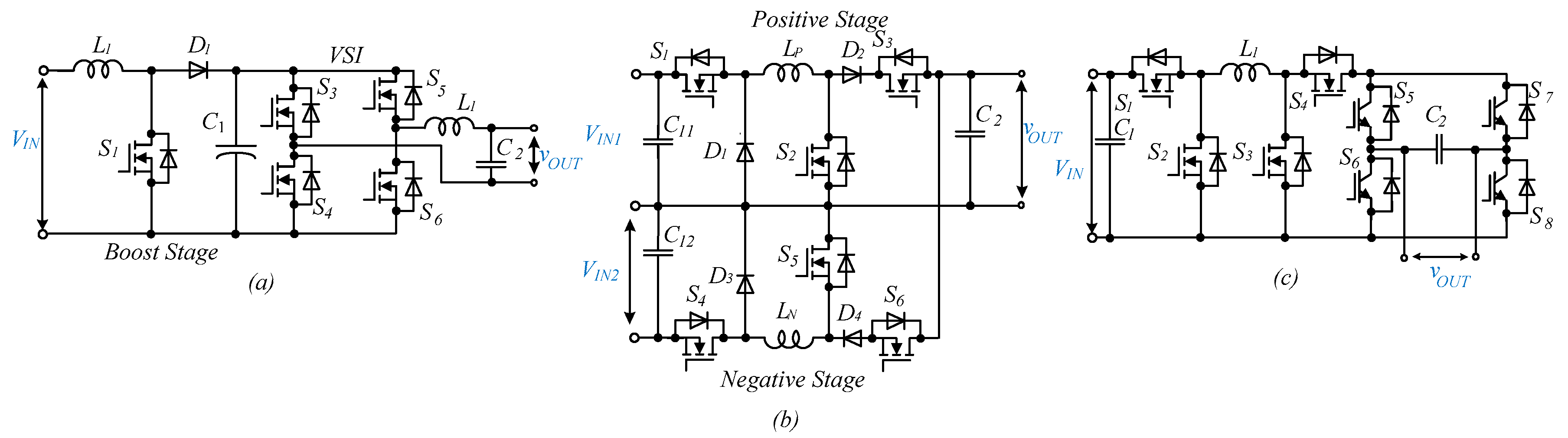
Figure 2.
Single-phase twisted single-stage bidirectional buck-boost dc-ac converter based on unfolding circuit.
Figure 2.
Single-phase twisted single-stage bidirectional buck-boost dc-ac converter based on unfolding circuit.

Figure 3.
Control system structure for the proposed solution (a) and closed-loop control equivalent circuit (b).
Figure 3.
Control system structure for the proposed solution (a) and closed-loop control equivalent circuit (b).
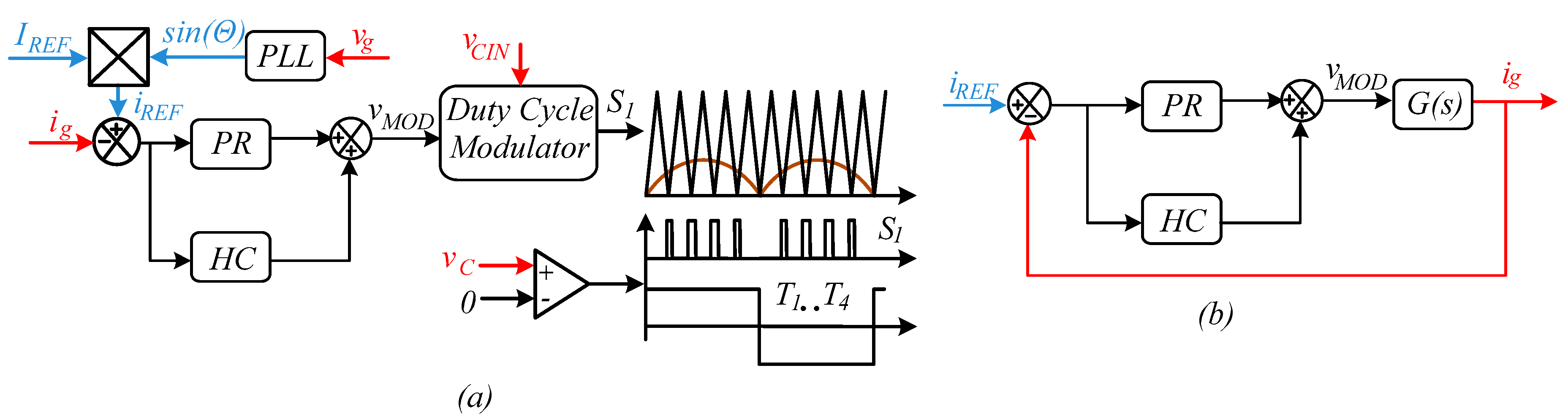
Figure 4.
Equivalent circuits of a twisted buck-boost converter-based unfolding: on-state of forward transfer (a), on-state of reverse transfer (b).
Figure 4.
Equivalent circuits of a twisted buck-boost converter-based unfolding: on-state of forward transfer (a), on-state of reverse transfer (b).

Figure 5.
Influences of the buck-boost on the passive elements at constant input power and current: the main inductance (a), the output capacitance (b), the output inductor filter (c).
Figure 5.
Influences of the buck-boost on the passive elements at constant input power and current: the main inductance (a), the output capacitance (b), the output inductor filter (c).
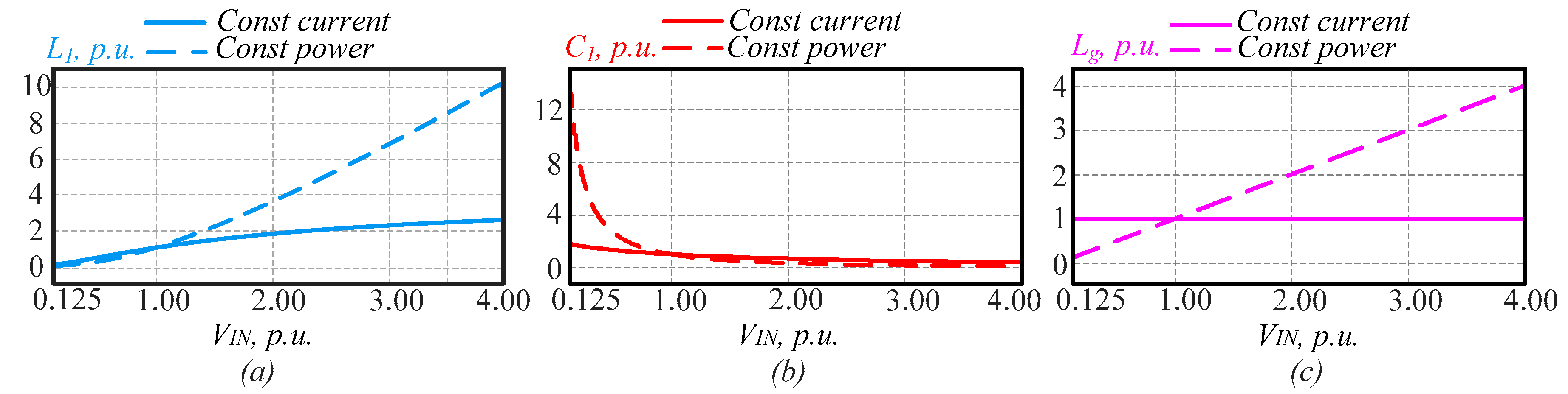
Figure 6.
Power losses estimation of the inverter: conduction losses of semiconductor switches (a), switching losses of transistors (b), efficiency estimation (c).
Figure 6.
Power losses estimation of the inverter: conduction losses of semiconductor switches (a), switching losses of transistors (b), efficiency estimation (c).
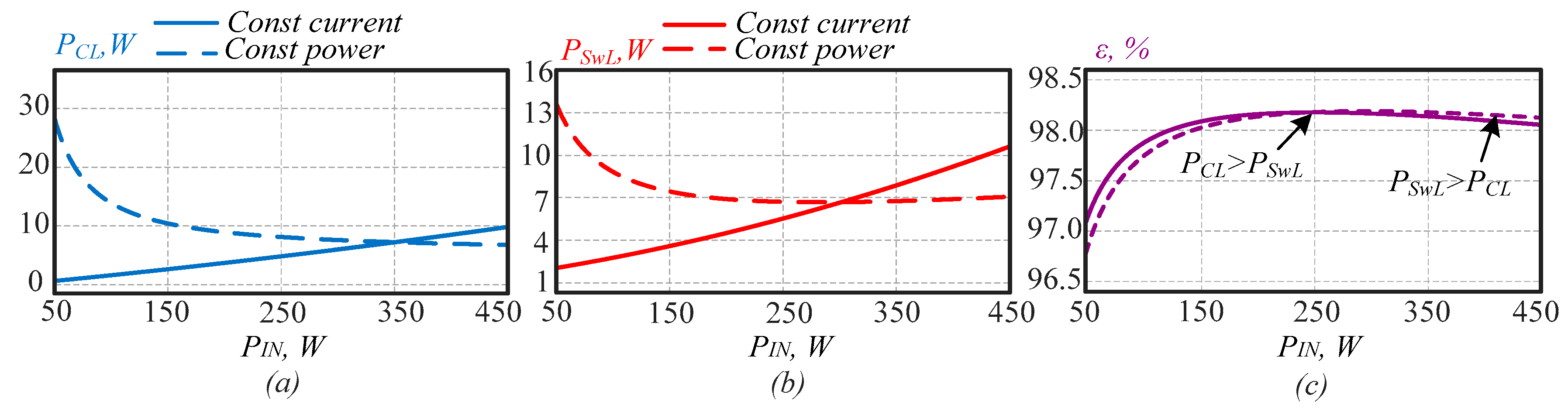
Figure 7.
Simulation results for Vout = 250 V, Pin = 250 W in rectifier mode (a) and inverter mode with Vin = 250 V (b).
Figure 7.
Simulation results for Vout = 250 V, Pin = 250 W in rectifier mode (a) and inverter mode with Vin = 250 V (b).
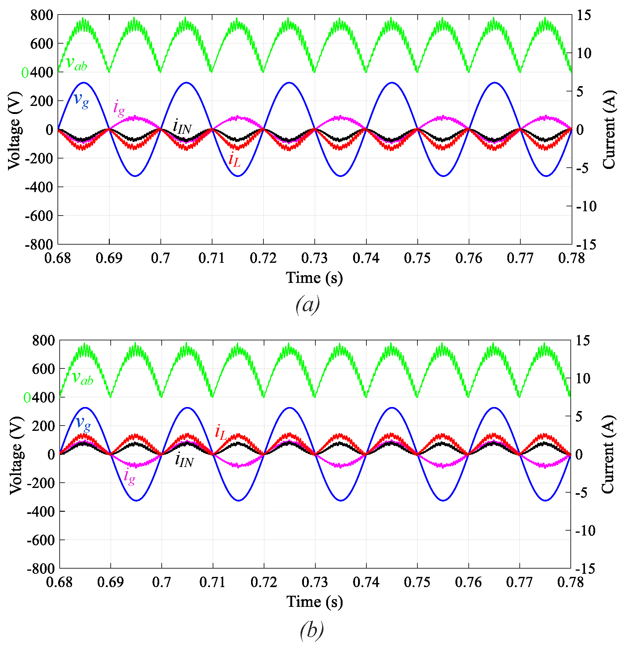
Figure 8.
Simulation results for Vin = 350 V, Pin = 850 W in rectifier mode (a) and inverter mode (b).
Figure 8.
Simulation results for Vin = 350 V, Pin = 850 W in rectifier mode (a) and inverter mode (b).

Figure 9.
Experimental setup of the twisted buck boost converter with unfolding circuit.
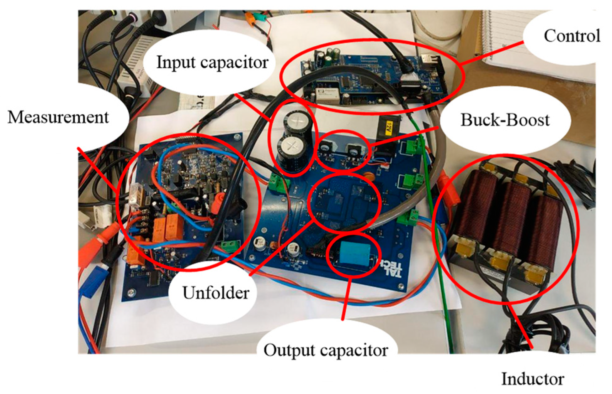
Figure 10.
Experimental results for Vin = 250 V, Pin = 250 W in the inverter mode without synchronous switching and separate control (a), without synchronous switching and with separate control (b), with synchronous switching and with separate control (c).
Figure 10.
Experimental results for Vin = 250 V, Pin = 250 W in the inverter mode without synchronous switching and separate control (a), without synchronous switching and with separate control (b), with synchronous switching and with separate control (c).

Figure 11.
Experimental results for Vin = 350 V, Pin = 850 W in the inverter mode without synchronous switching and separate control (a), without synchronous switching and with separate control (b), with synchronous switching and with separate control (c).
Figure 11.
Experimental results for Vin = 350 V, Pin = 850 W in the inverter mode without synchronous switching and separate control (a), without synchronous switching and with separate control (b), with synchronous switching and with separate control (c).
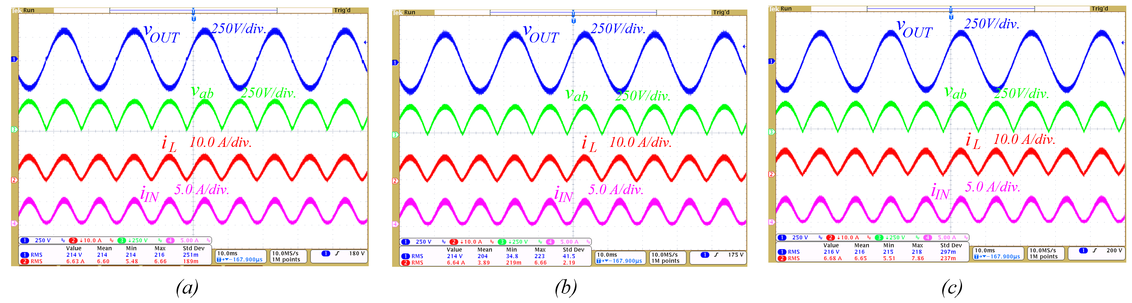
Figure 12.
Experimental results of the grid-connected converter in the inverter mode.

Figure 13.
Efficiency versus input power in unidirectional mode with constant input voltage (a), efficiency versus input voltage with constant input power (b).
Figure 13.
Efficiency versus input power in unidirectional mode with constant input voltage (a), efficiency versus input voltage with constant input power (b).

Figure 14.
Efficiency versus input power in the bidirectional mode with constant input voltage (a), efficiency versus input voltage with constant input power (b).
Figure 14.
Efficiency versus input power in the bidirectional mode with constant input voltage (a), efficiency versus input voltage with constant input power (b).
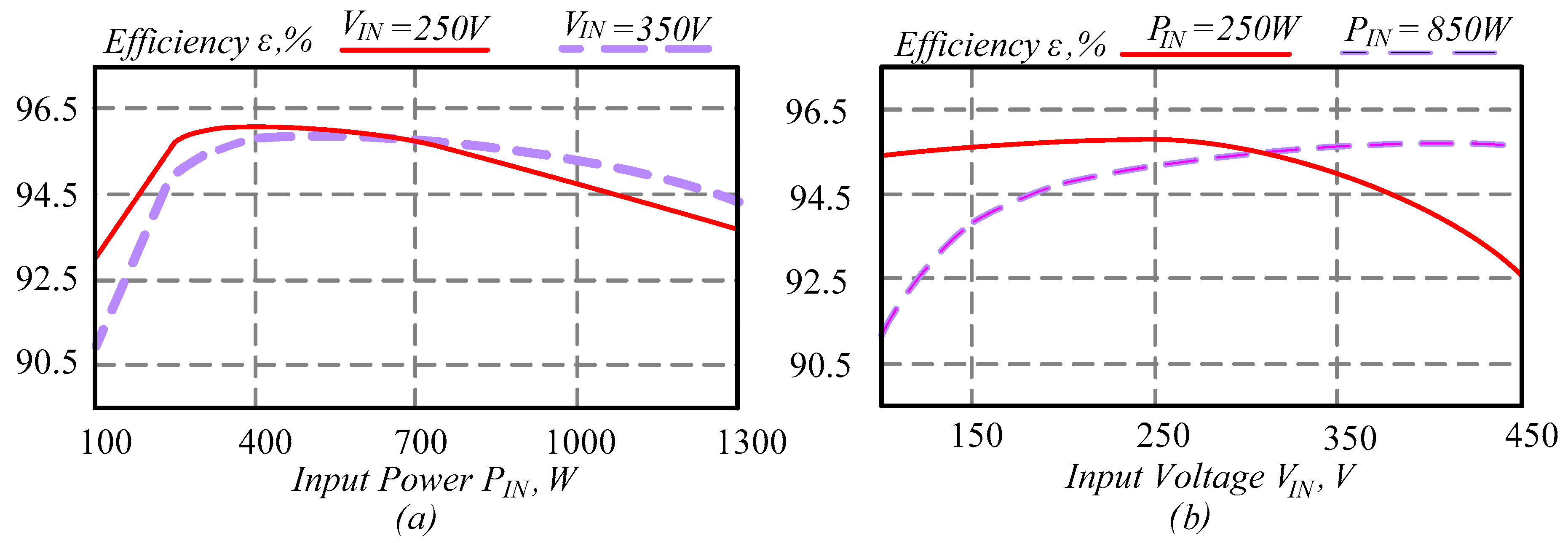
Figure 15.
Efficiency study of the proposed solution in the unidirectional mode: thermal picture for 250 V and 550 W (a,b), and 350 V, 1150 W (c,d).
Figure 15.
Efficiency study of the proposed solution in the unidirectional mode: thermal picture for 250 V and 550 W (a,b), and 350 V, 1150 W (c,d).

Figure 16.
Losses distribution for 550 W at 250 V input voltage (a) and 1150 W at 350 V (b) input voltage.
Figure 16.
Losses distribution for 550 W at 250 V input voltage (a) and 1150 W at 350 V (b) input voltage.


Table 1.
Passive components used for simulation verification.
| Passive Components | Value |
|---|---|
| Input capacitor, C1 | 330 uF |
| Inductor, L1 | 1800 uH |
| Unfolding capacitor, C2 | 2.1 uF |
| Grid side inductor, L2 | 670 uH |
| Switching frequency | 60 kHz |
| Sampling frequency | 15 kHz |
© 2019 by the authors. Licensee MDPI, Basel, Switzerland. This article is an open access article distributed under the terms and conditions of the Creative Commons Attribution (CC BY) license (http://creativecommons.org/licenses/by/4.0/).
Share and Cite
MDPI and ACS Style
Husev, O.; Matiushkin, O.; Roncero-Clemente, C.; Vinnikov, D.; Chopyk, V. Bidirectional Twisted Single-Stage Single-Phase Buck-Boost DC-AC Converter. Energies 2019, 12, 3505. https://doi.org/10.3390/en12183505
AMA Style
Husev O, Matiushkin O, Roncero-Clemente C, Vinnikov D, Chopyk V. Bidirectional Twisted Single-Stage Single-Phase Buck-Boost DC-AC Converter. Energies. 2019; 12(18):3505. https://doi.org/10.3390/en12183505
Chicago/Turabian StyleHusev, Oleksandr, Oleksandr Matiushkin, Carlos Roncero-Clemente, Dmitri Vinnikov, and Vasyl Chopyk. 2019. "Bidirectional Twisted Single-Stage Single-Phase Buck-Boost DC-AC Converter" Energies 12, no. 18: 3505. https://doi.org/10.3390/en12183505
Note that from the first issue of 2016, this journal uses article numbers instead of page numbers. See further details here.