A Different Voltage-Source Power Inverter with Carrier Based SPWM for Open-End Connection Loads

1
Department of Electrical Engineering, Jenderal Soedirman University, Purwokerto 53112, Indonesia
2
Department of Electrical and Electronics Engineering, Shizuoka University, Hamamatsu 432-8011, Japan
*
Author to whom correspondence should be addressed.
Energies 2019, 12(17), 3251; https://doi.org/10.3390/en12173251
Submission received: 29 July 2019
/
Revised: 12 August 2019
/
Accepted: 17 August 2019
/
Published: 23 August 2019
Abstract
:This paper presents a new configuration of voltage source inverter with a simplified circuit for generating five-level pulse width modulation (PWM) voltage waveform. Compared with conventional inverter configuration, this circuit is drastically able to simplify the structure and reduce the required number of active switch components. The new inverter circuit is very suitable for the use of open-end connection loads such as open-end winding ac motor drive application. Instead of using separated dc power sources, the new inverter circuit configuration is also possible to utilize only one dc voltage source, so the power supply circuits can be made simpler. Furthermore, to reduce ripples of dc capacitor voltages, the voltage stabilizing circuit of capacitors at the input side was proposed and applied. The stabilizing circuit is capable to work reducing the size of dc capacitors, and maintaining voltage stability of capacitors through charging and discharging operation modes. The working principles of inverter circuit were evaluated and examined by means of computer simulations using PSIM software. In addition, experimental test results of the prototype were also provided. Test results proved that the new five-level PWM inverter operated well generating five-level output waveform with smaller distortion and less voltage ripples of dc capacitors.
1. Introduction
A multilevel inverter is a type of inverter working to produce ac voltage or ac current waveforms with three or more level numbers of waveforms [1,2,3]. When the input source is a dc voltage, the inverter is categorized as a voltage source inverter. However, if the input is in the form of dc current source, the inverter circuit is included as the current source inverter type [4]. In a regular two-level voltage source inverter, output voltage before the filter circuit is a discrete ac voltage waveform with a large dv/dt value, whereas in the two-level current source inverter, the output current wave before the filter is a discrete ac current wave with a large di/dt value.
Multilevel inverters are able to work generating ac output voltages or currents with a smaller distortion value, smaller filter size, smaller dv/dt or di/dt value, and the ability to work at a greater power capacity [5,6]. Multilevel inverters are very suitable for use in a medium and large variable speed ac motor drive. The three popular multilevel inverter configurations are the cascaded H-bridge inverter, diode clamped inverter and flying capacitor inverter [7,8,9,10,11]. Each configuration has its own disadvantages and advantages. The first topology connects some H-bridge inverters in a series to synthesize multilevel voltage waveform. Each inverter uses an isolated dc power source. As a result, more complex dc power source circuits are required when the power sources are rectifier systems. However, when the dc sources are batteries of renewable power generations, the inverter system is very suitable. The diode clamped multilevel inverter needs additional diodes in addition to the controlled power switches, hence conduction losses of diodes will append the total losses of inverter circuits. The third topology is the flying capacitor multilevel inverter. In this inverter circuit, the voltage balance and their control complexity are the main issues causing other constraints of its application [12,13].
In an ac motor drive system, the conventional winding configurations of wound rotor type induction motor coils are the star and delta winding connections. In addition to these two types of entanglement, there is another winding connection, namely open-end connection winding ac motor. This type of motor drive has some merits compared to the conventional delta and star connections. Using open-end connection loads, the phase current of each phase can be controlled independently. When using multi sources of inverter system, the capacity of inverter can be smaller than the motor rating [14,15,16,17].
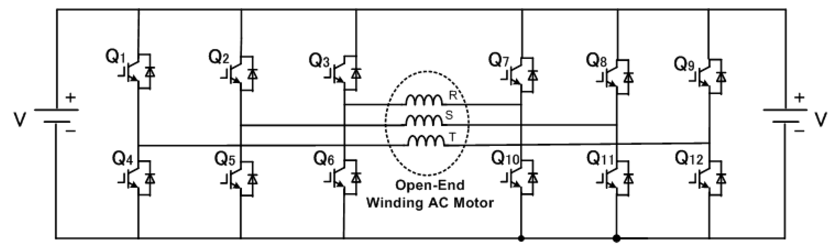
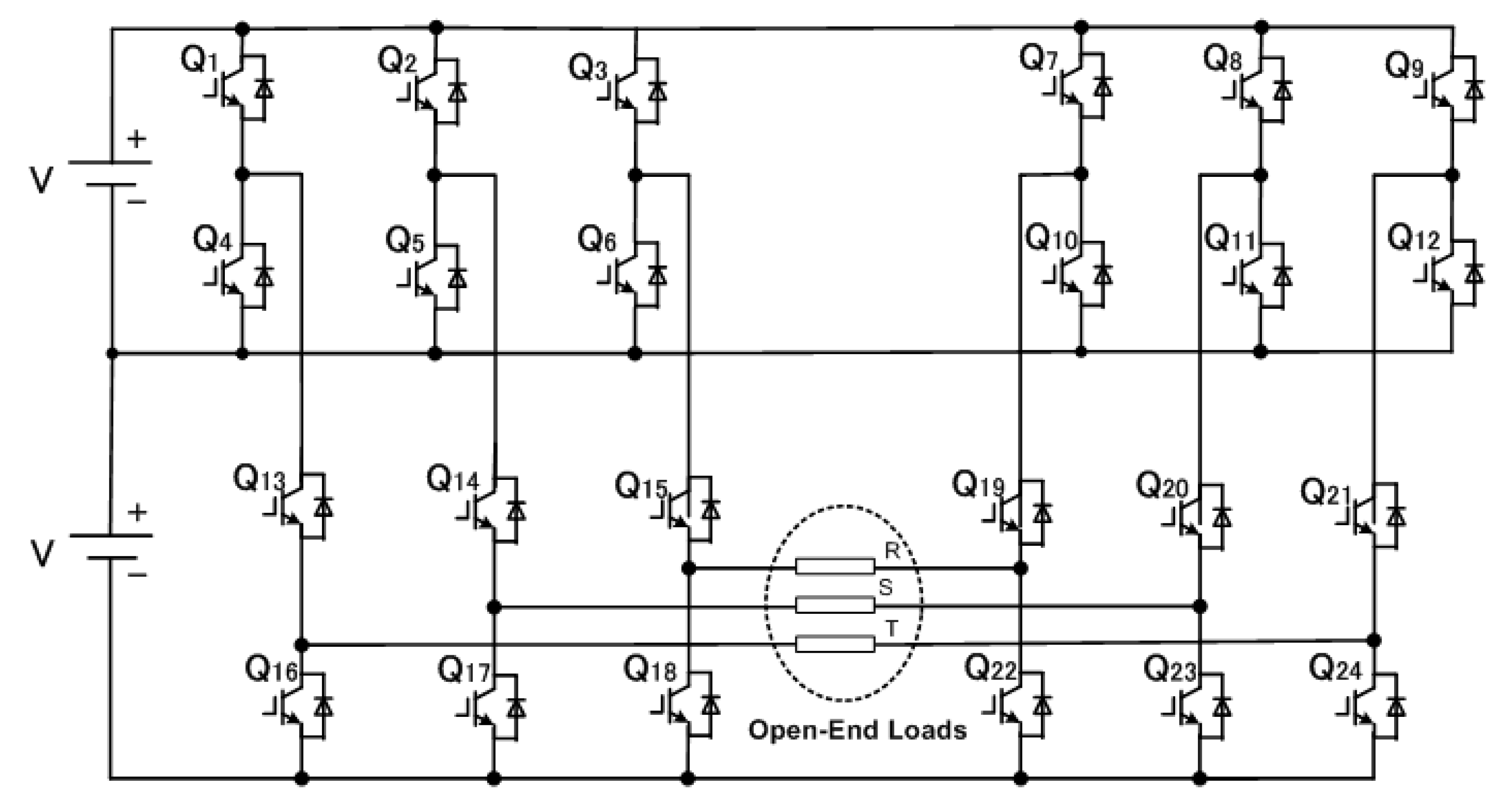
In a practical manner, the open-end winding connection of an ac motor can be obtained facilely by opening the neutral motor windings. There is no need to change or modify the mechanical structure of the motor. This kind of motor drive has been started to be developed by researchers and industries for various possible applications, such as pumping systems and electric car systems [18,19,20,21]. An important aspect in the development of open-end connection winding ac motor drive is the development of inverter systems which are different with the inverter circuits for common delta and star connection loads [22,23,24,25,26]. Figure 1 displays a conventional circuit of a three-level inverter used for the driving of open-end winding ac motors [14,24]. To get a more level number of voltage wave with smaller waveform distortion and higher power capacity, Figure 2 presents the conventional structure of a five-level inverter presented in Reference [27] used for open-end connection loads. This inverter circuit needs 24 controlled power switches in total to construct the inverter where each controlled switch such as IGBT, thyristor or power MOSFET needs individual gate drive circuit. Hence, the more controlled switches used, the more complex the gate drive system will be required to be. In the multilevel inverter circuits, power device number and circuit complexity are some problems that need to be addressed. Simplifying the inverter circuit is a good way to make multilevel inverter circuits more interesting to be applied because of their features. The aim of this work is to develop a novel configuration of five-level voltage source inverter with simpler circuit configuration for open-end connection load application.
In this manuscript, a different circuit of five-level PWM inverter for open-end connection loads is proposed and discussed. The newly recommended inverter circuit has a main merit in simplifying the inverter circuit configuration by reducing the required controlled switches number and their gate drive circuits. The possibility of using a single dc power source with smaller dc capacitors is another advantage of this new inverter. The basic operations of the proposed five-level inverter were explored and tested using computer simulations and experiments in laboratory.
2. Proposed New Inverter Circuit
2.1. Proposed Inverter Circuit Configuration with Two DC Sources
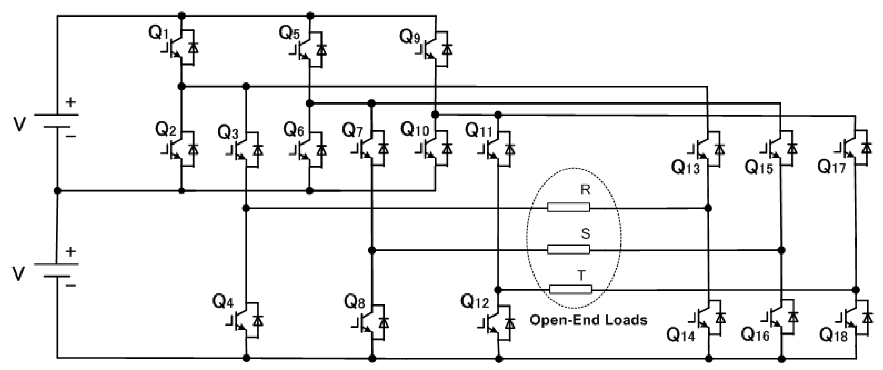
Figure 3 presents the circuit configuration of the proposed five-level inverter with two dc power sources. In this inverter circuit, the two dc power sources can make use of rectifiers or the battery system. The dc input power sources have the same voltage of V. This inverter circuit needs 18 controlled switches in total to result in a five-level three-phase output voltage waveform. Compared to the conventional circuit presented in Reference [28], a total of six power switches can be reduced. Moreover, the gate drive circuits are also much simpler. A comparison table outlining the merits of the proposed five-level inverter and conventional circuit is presented in Table 1. The proposed inverter is feasible to operate with one dc power source as will be discussed later.
Table 2 lists the switching combinations to yield five-level voltage waveform of phase R from two dc input power sources. The inverter is connected to a three-phase open-end connection load. The inverter circuit generates a five-level voltage waveform, i.e., +2V, +V, 0, −V, −2V level voltages as shown in Table 2. The output voltages of the other two phases are similar, but differ in phase 1200 for each phase.
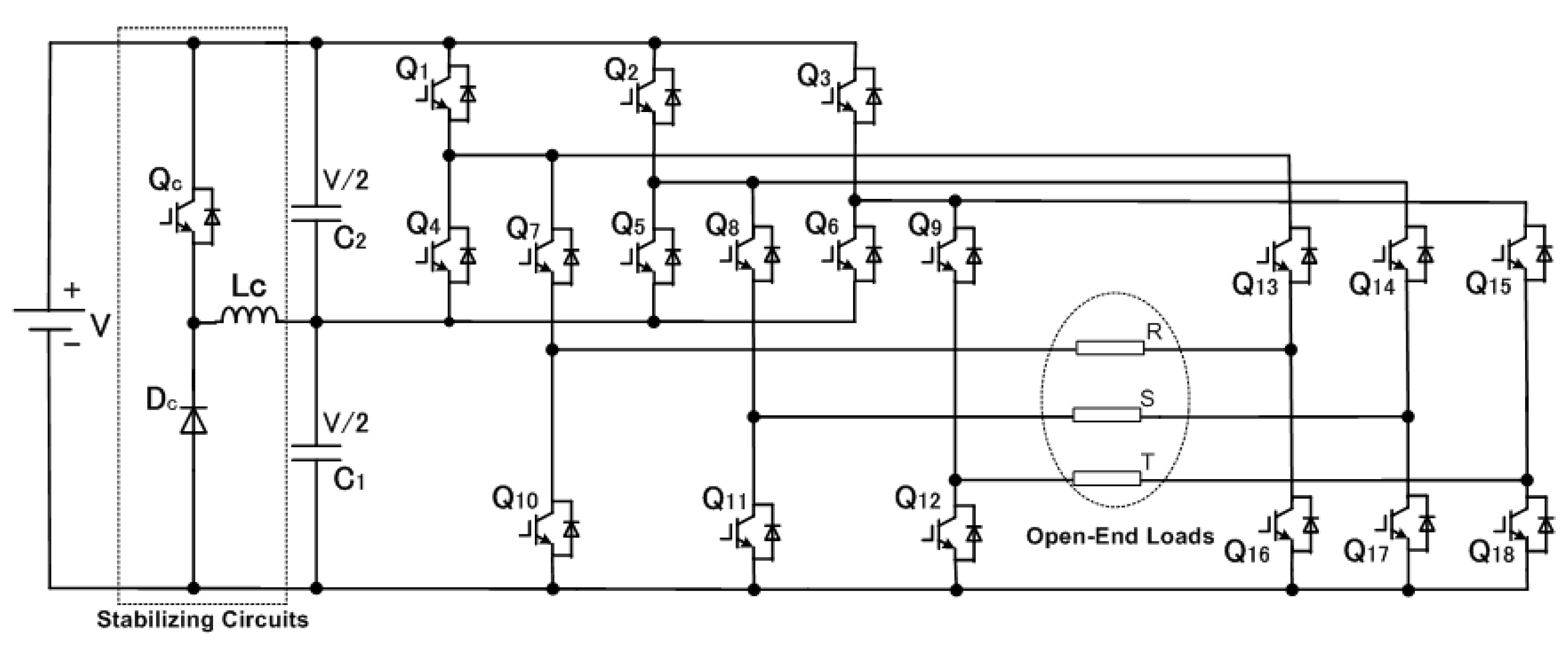
2.2. Proposed Inverter Circuit Configuration with Single DC Power Source
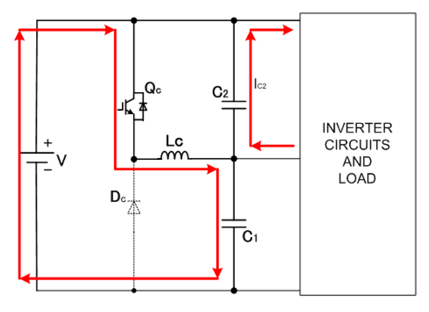
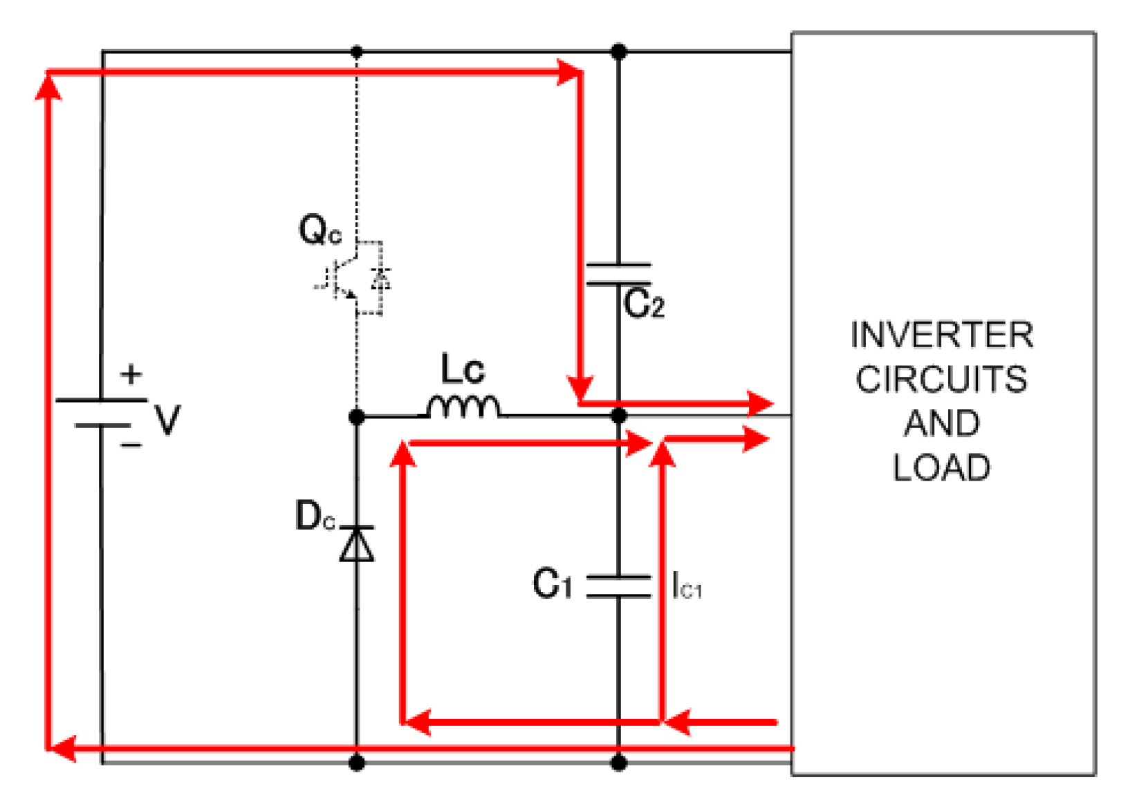
In order to simplify the input dc power source number, Figure 4 presents the proposed three-phase five-level PWM inverter with only one dc voltage source. A simple stabilizing circuit was connected across the dc capacitors C1 and C2 to keep stable voltage across capacitors, reduce ripples, and minimize the capacitor size. The operation modes of the stabilizing circuit are presented in Figure 5 and Figure 6. In this stabilizing circuit, the power switch Qc will regulate the charging and discharging states of inductor Lc, and capacitors C1 and C2. The minimum inductor size of Lc for continuous current mode can be determined as follows:
where Lc is the stabilizing inductor, D is the duty cycle of control signal of switch Qc, fQc is the switching frequency of switch Qc, and R is the resistance of power load.
The dc capacitor C1 experiences charging state when the switch Qc is turned-on, while capacitor C2 is in discharging state. Discharging mode of capacitor C1 occurred when the switch Qc is turned-off, whilst capacitor C2 is in charging mode, as depicted in the figures. The ripple factor (r) of capacitor voltage can be calculated as follows:
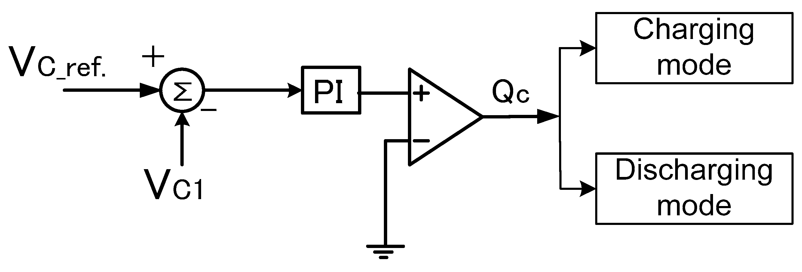
Figure 7 acquaints the control diagram of dc capacitors with the stabilizing circuit [27]. The system needs only one voltage sensor placed at the capacitor terminal C1. The voltage of capacitor C1 will be determined by the setting command value (VC-Ref) of proportional integral (PI) controller as indicated in the figure, while the voltage of capacitor C2 is the dc input voltage subtracted by the voltage VC1 in capacitor C1.
2.3. PWM Modulation Strategy
Ideally, an ac power load draws sinusoidal current to supply its electric power. Power inverter is a static converter converting dc input power into ac power in addition to the ac generator machine working as rotating converter in a power generation system. The ideal ac waveform is a sinusoidal current or voltage waveform. However, in many practical cases the ac power generations do not generate sinusoidal voltage or current perfectly. The voltage drops in electrical components or the imperfect operation of machines or controllers will contribute to this waveform distortion phenomenon.
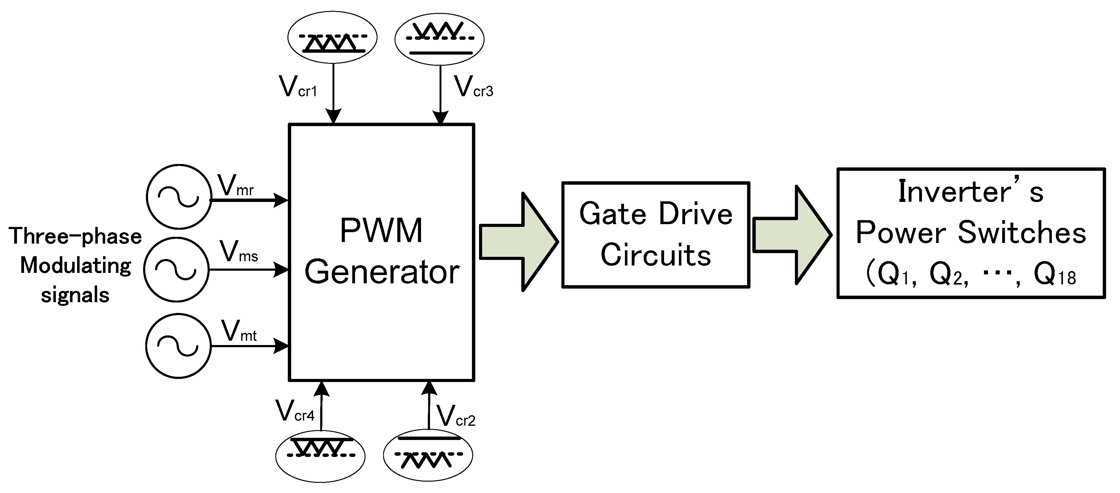
In a power inverter, the PWM switching pattern is applied to generate PWM voltage or current waveform. This PWM voltage will have smaller distortion compared to the square wave operation of voltage or current. Many modulation strategies have been introduced, presented and used in the inverter circuits commercially available or the inverter circuits which are still under development. Carrier based sinusoidal pulse width modulation (SPWM) technique is one of the modulation techniques that alternatively can be applied to generate PWM voltage or PWM current waveform. This modulation is able to reduce distortion of the ac current and voltage. Furthermore, this method can be handily implemented by using analog or digital circuits for a higher level number waveform. In this method, saw-tooth or triangular signals are compared with sinusoidal waves to generate PWM patterns of inverter’s gating signals as shown in Figure 8. The switching frequency can be regulated by adjusting the frequency of triangular carriers, and the fundamental frequency is controlled by the modulating signal [29,30].
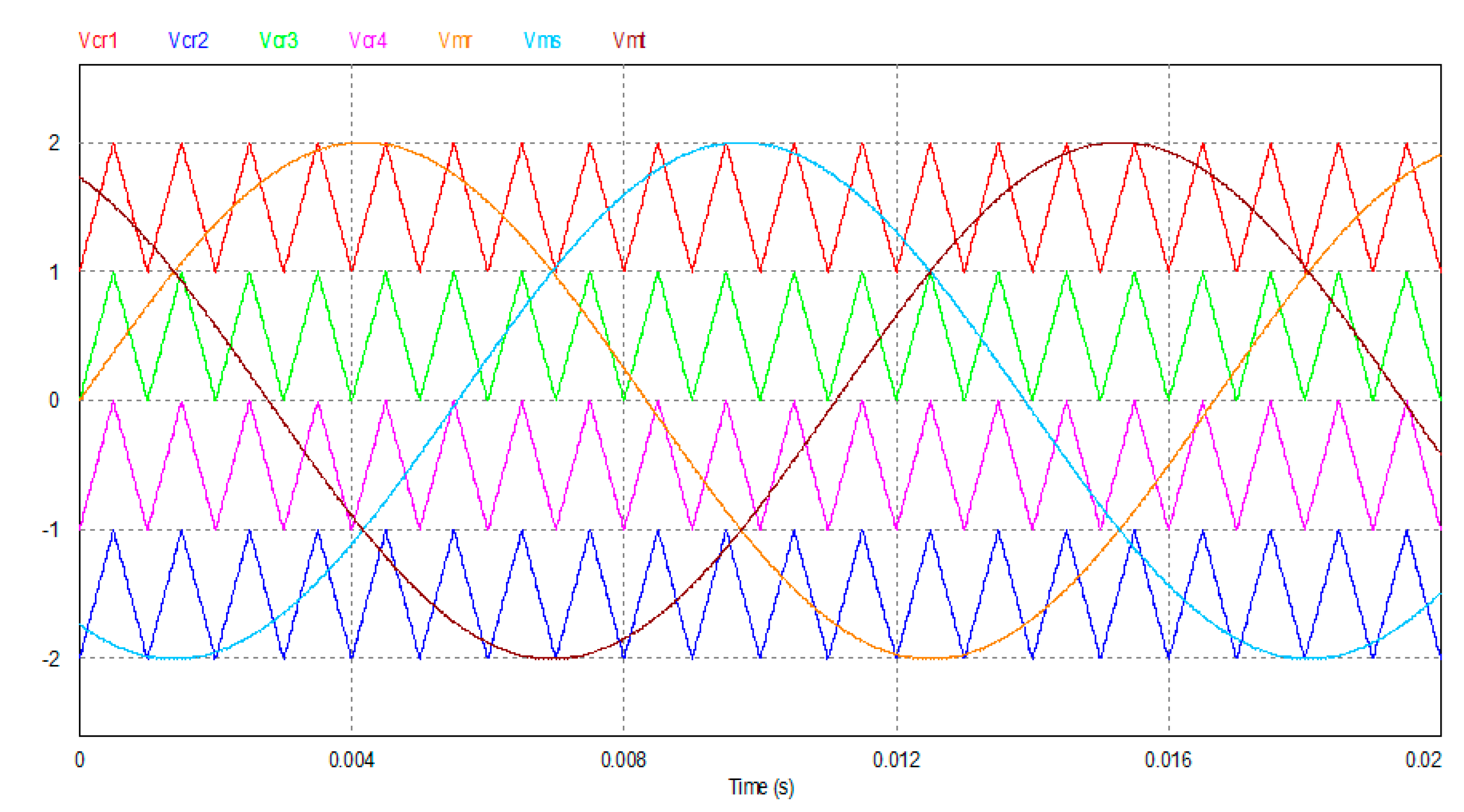
This paper applied multi carrier waveforms with different offset values but with the same frequency as depicted in Figure 9. The carrier signals are Vcr1, Vcr2, Vcr3 and Vcr4. They have the same amplitude and frequency. In case of a three-phase inverter system, the modulating signals are Vmr, Vms and Vmt. The modulation index (Mi) can be determined by the equation below:
where Vm and Vcr are the amplitudes of modulating and carrier signals, respectively. The amplitude of fundamental voltage is proportional to the modulation index. The switching harmonics component and its sideband are normally located centered at:
where hsw is the switching harmonics component, k is an integer and fcr is the triangular frequency. This modulation method can be easily extended for higher level number of voltage waveform by adding more carriers with appropriate offset values.
3. Test Results and Discussion
3.1. Computer Simulation Examinations
To explore and verify the accuracy of the principle and the performance of the proposed inverter, computer simulations of the circuit were conducted using PSIM software. The inverter circuit equipped with the balancing circuit of Figure 4 was tested. Parameters of inverter are detailed in Table 3. A 100 V dc voltage source was applied to the input side of the inverter. An open-end connection power load system, i.e., resistor 20 Ω, and inductor 5 mH was connected to the each phase output terminal of inverter circuit. The inverter switches were operated at 22 kHz. It was high enough to avoid audible noise during switching operation. The fundamental frequency of output current and voltage waveforms was set as 50 Hz. The modulating signal of PWM circuits can be adjusted to change the modulation index.
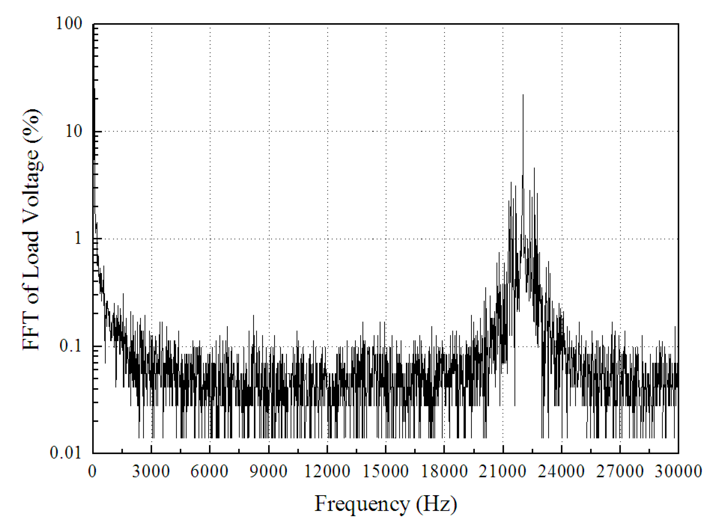
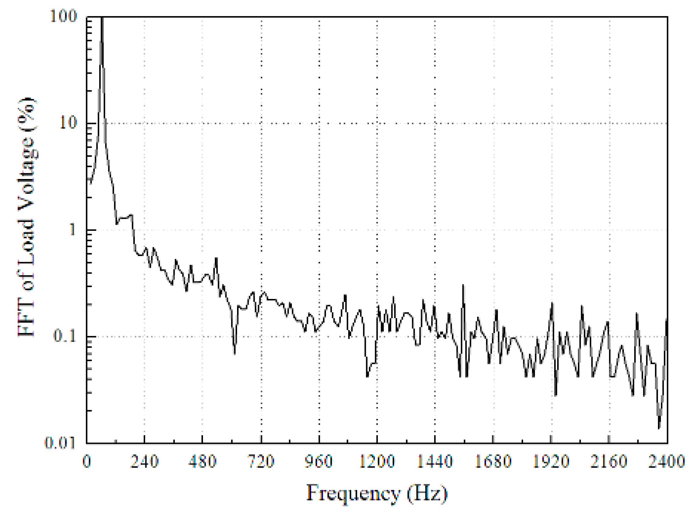
Figure 10 presents inverter’s output waveforms when the modulation index was 0.975. From the measured waveforms, it can be viewed that a five-level PWM voltage waveform of phase voltage was properly produced by the developed inverter. Furthermore, perfect three-phase sinusoidal load currents were generated to the loads. Figure 11 and Figure 12 present the harmonics profiles of the produced five-level PWM voltage wave for frequency range 0–30 kHz and 0–2400 Hz, respectively. The five-level PWM voltage waveform contained switching harmonics components around 22 kHz and its multiples. The amplitude of the 3rd harmonics component is about 1.5% which is much lower according to the standard IEEE 519.
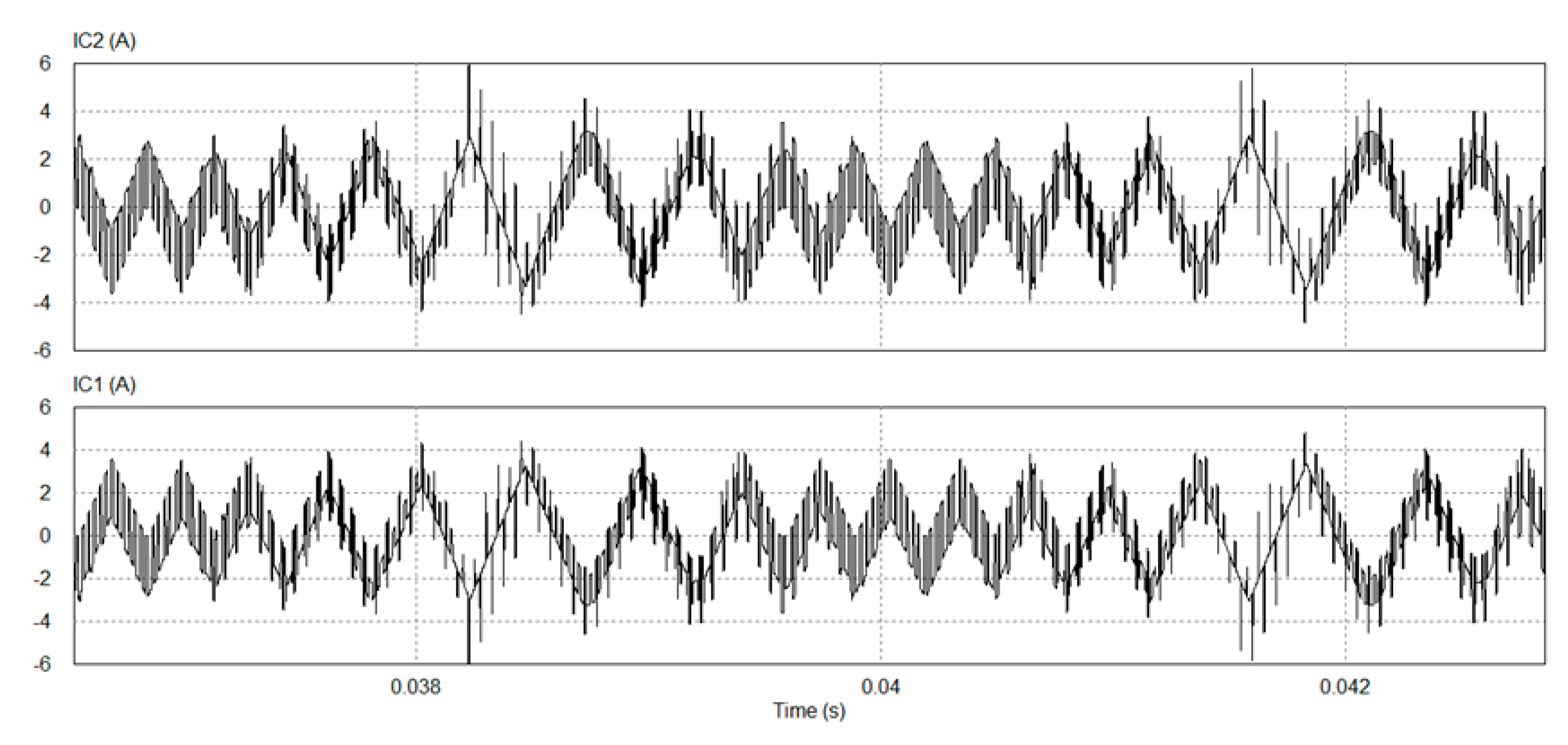
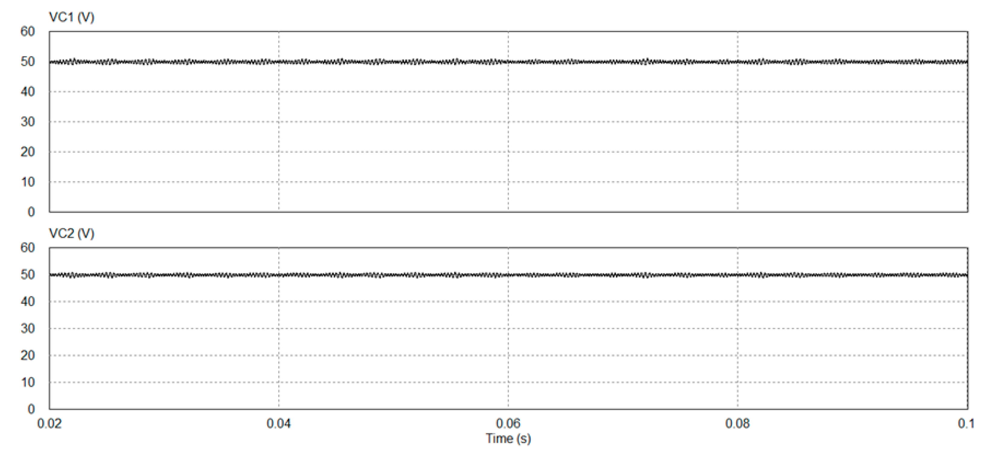
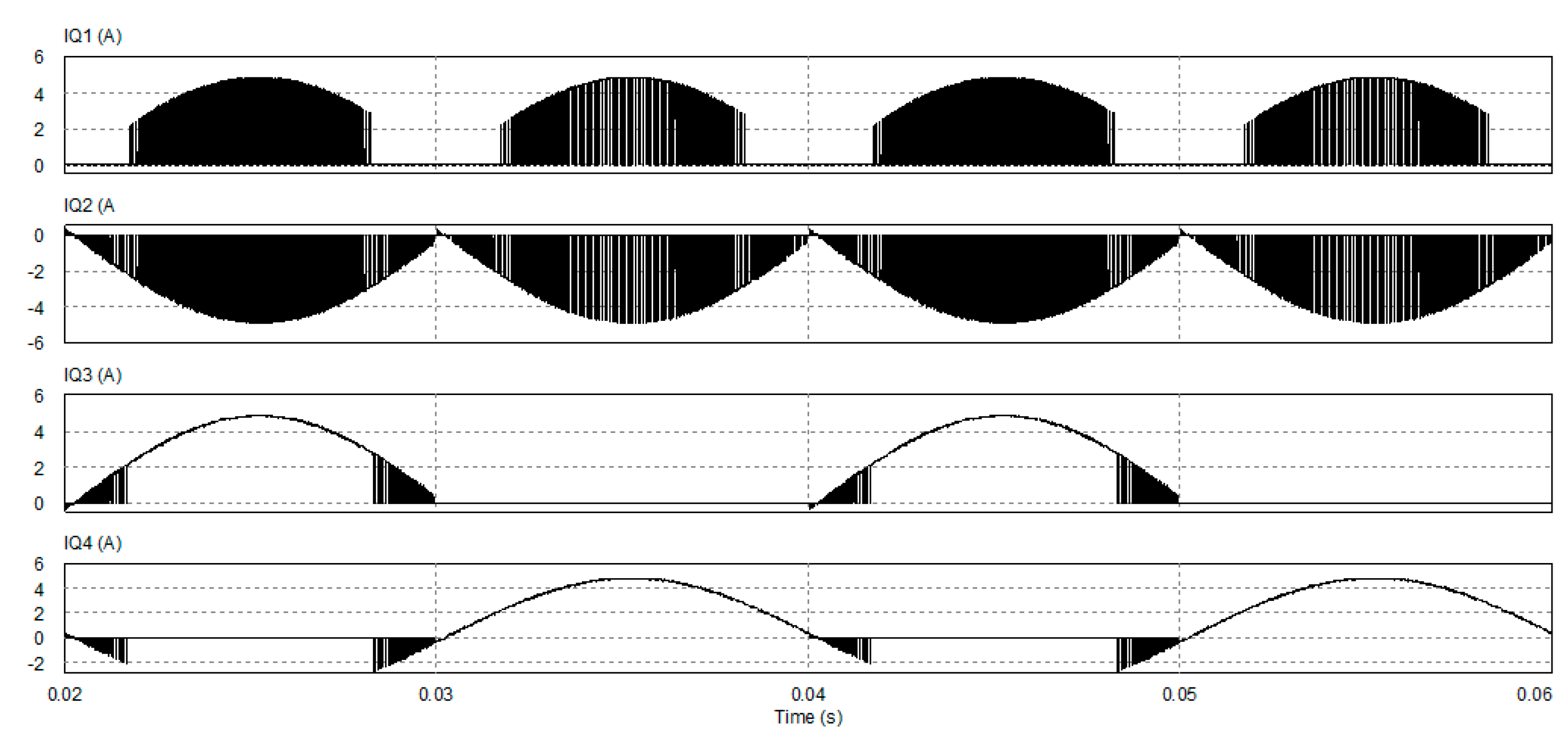
Furthermore, the enlarged current waveforms of capacitors during the charging and discharging modes of the 100 µF dc capacitors C1 and C2 are presented in Figure 13. These currents were the currents flowing through the capacitors. The controller worked regulating the capacitor’s states, i.e., charging and discharging modes to maintain stable voltage of the capacitors C1 and C2. Figure 14 is the voltage waveform of dc capacitors C1 and C2. The measured ripple of the capacitor voltages was 1.1%. Even with small capacitors used, the ripple of capacitors was relatively small. The current waveforms flowing through the inverter’s power switches are shown in Figure 15. The magnitudes of these currents are the same. They have PWM patterns associated with the switching frequency of inverter switches.
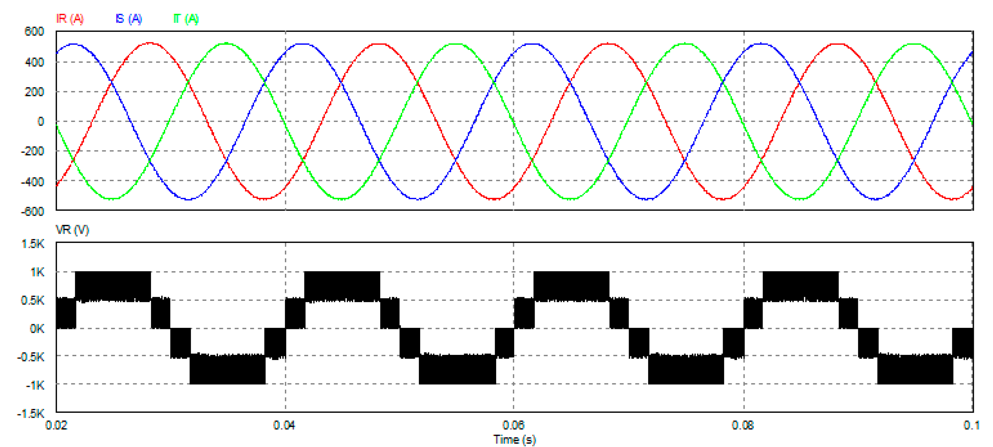
We can improve the output power and power rating by increasing the dc input voltage, and choose the appropriate power switches to meet the power load requirement. Figure 16 presents the simulation results when the dc input voltage is 1000 V, with power load resistor 1 Ω, inductor 5 mH. The peak load current is about 600 A. There was no problem for higher power and low power factor operation of the proposed inverter.
3.2. Experimental Examinations
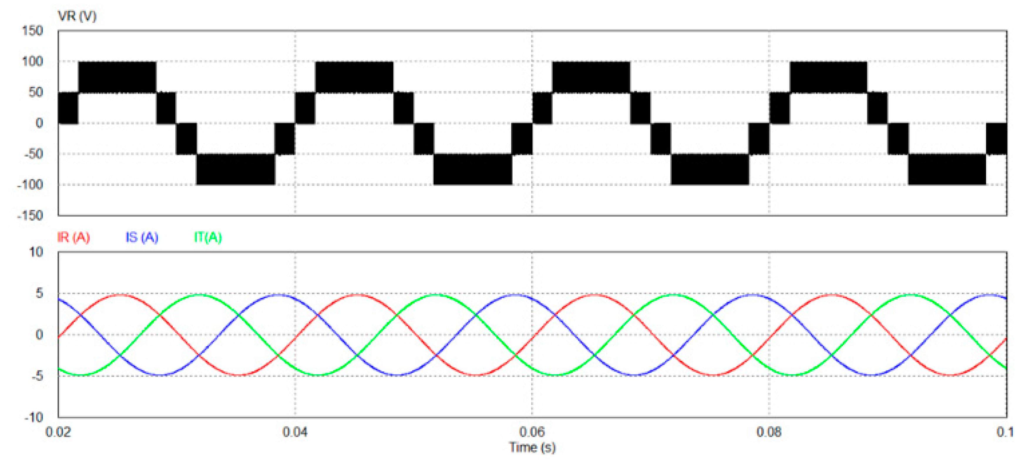
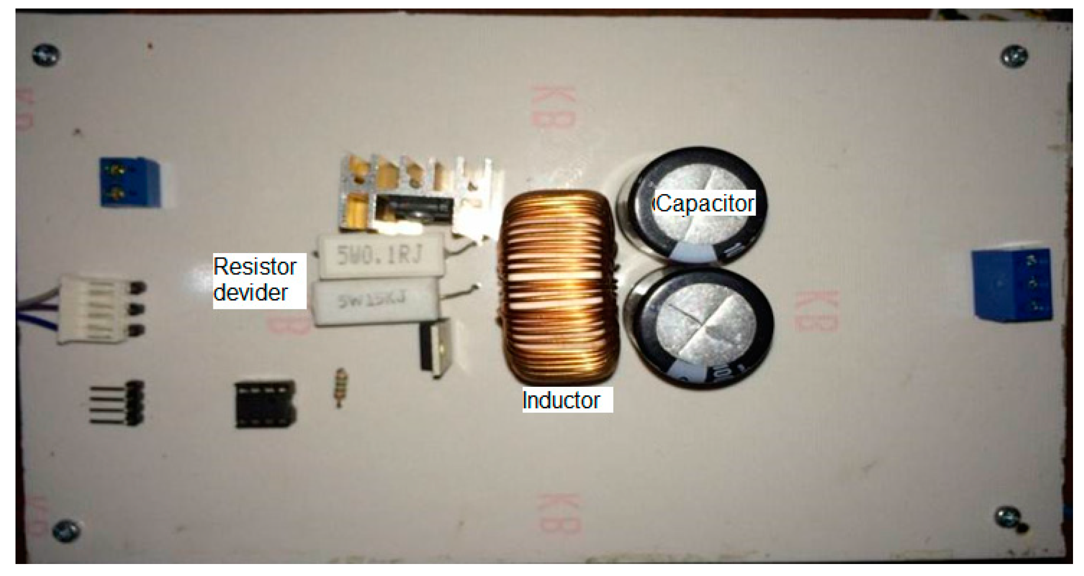
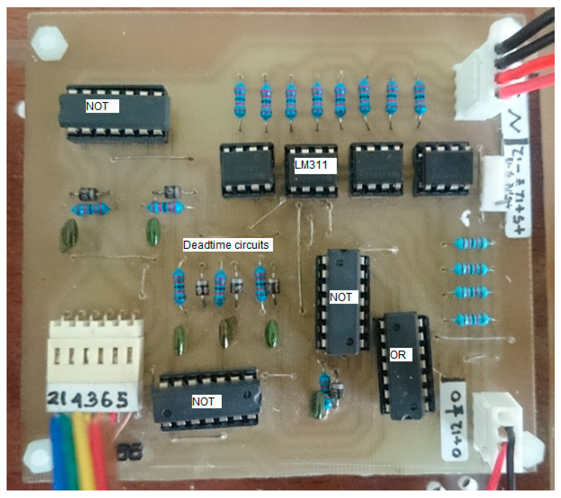
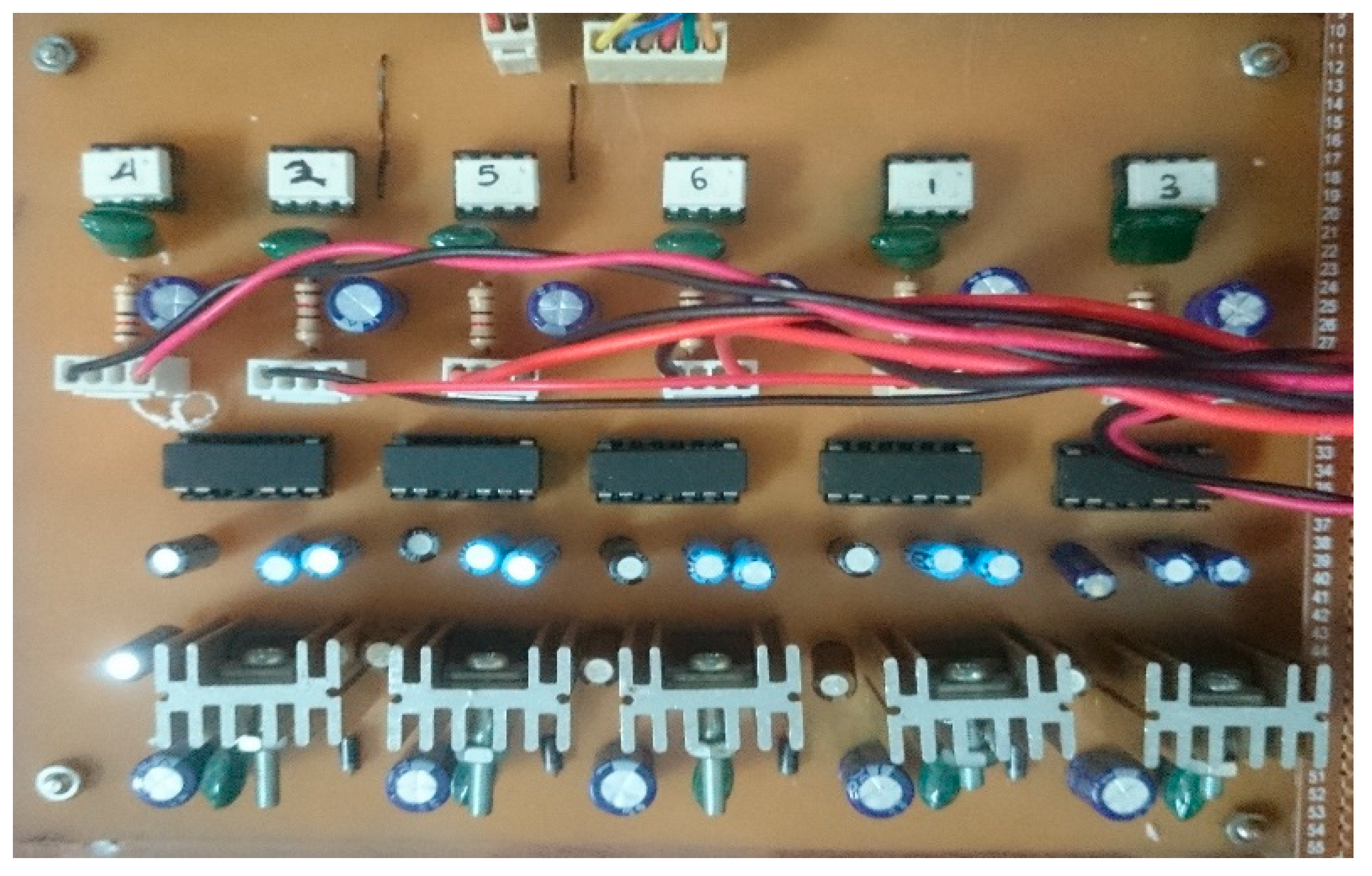
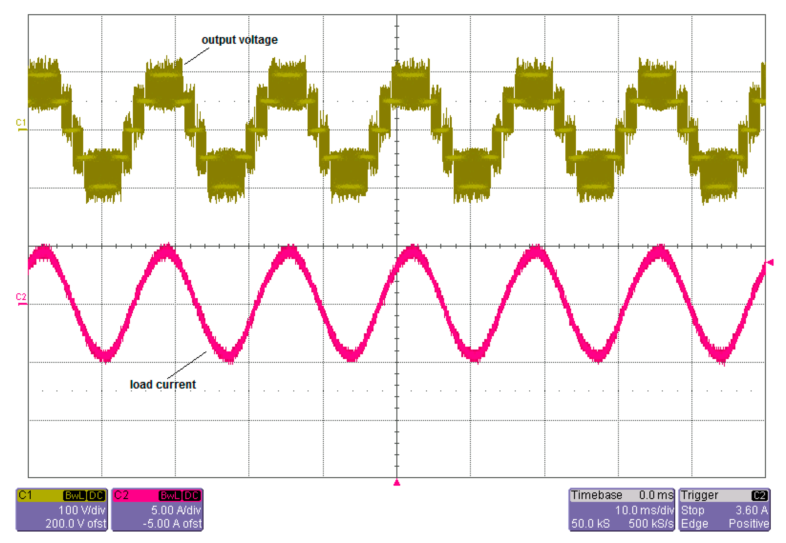
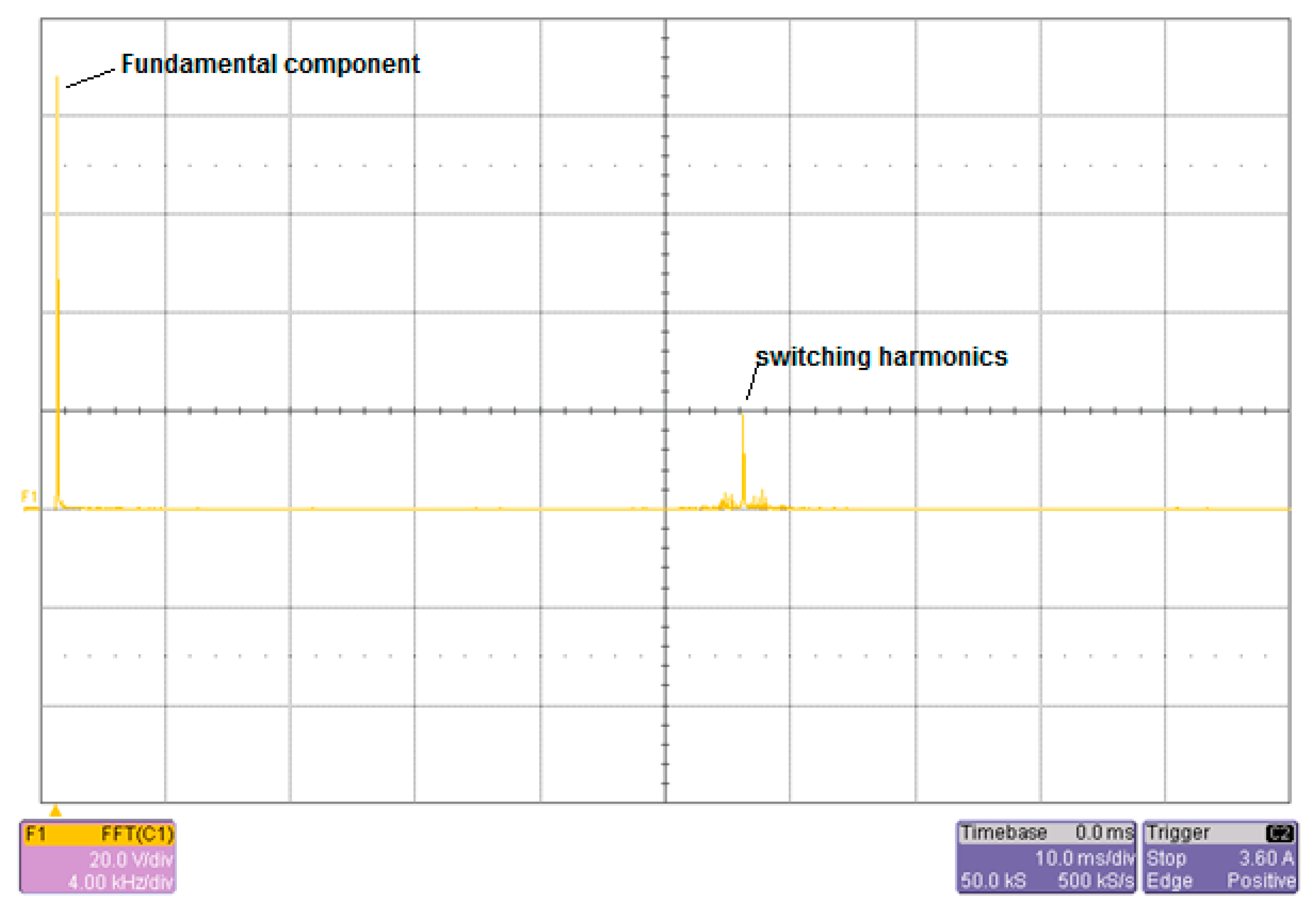
Using a 100 V dc power source obtained from a dc voltage regulator, the proposed inverter was tested experimentally. The inverter power switches were constructed by power diode DSEI120, and power MOSFETs FK30SM-6 as shown in Figure 17, with switching frequency 22 kHz. The size of stabilizing inductor was chosen as 100 µH. The voltage sensor was realized by using resistor divider circuits 33 kΩ and 5.6 kΩ as shown in Figure 18. To ensure the inverter operates properly, a 2 µs dead-time was inserted to the gating signals of inverter circuits. Realization of dead-time circuits is shown in Figure 19. The inverter circuit applied TLP250 as gate drive circuits of inverter’s MOSFET as shown in Figure 20. The TLP250 circuits were supplied by using DCP020515. The inverter circuit was connected to 20 Ω resistors in series with 5 mH power inductors as in simulation test. The measured output waveforms of voltage and current for phase R are shown in Figure 21. Five-level voltage and sinusoidal current were confirmed experimentally. The results give more opportunity for further application of the newly developed inverter. The measured harmonics components including the switching harmonics are presented in Figure 22.
4. Conclusions
In this research paper, a new variant of three-phase five-level voltage source power inverter with minimized component number was proposed and discussed. The new inverter circuit can reduce six power switches, three isolated gate drive circuits and six gate drive circuits compared with a conventional inverter. The new inverter circuit is suitable for open-end connection load. Results of computer simulation and laboratory experimental tests confirmed that five-level voltage waveforms were properly produced by the proposed inverter. Furthermore, when single dc power source was employed to the inverter, the stabilizing circuit worked well maintaining stable dc voltage of capacitors, even when the small sized capacitors were used. Small ripple 1.1% of capacitor voltages were also confirmed with 100 µF dc capacitors. From the harmonics analysis results of the PWM voltage waveform, it can be viewed that most of low harmonic amplitudes were less than 2% compared to the fundamental component.
Author Contributions
S. and T.N. designed the inverter circuit configuration including the main power circuits, stabilizing circuits and controller. D.T.N. helped in the hardware design, and experimental set up.
Funding
This research was funded by Ministry of Research, Technology and Higher Education, republic of Indonesia.
Conflicts of Interest
The authors declare no conflict of interest.
References
- Rodriguez, J.; Lai, J.-S.; Peng, F.Z. Multilevel inverter: A survey of topologies, controls, and application. IEEE Trans. Ind. Electron. 2002, 49, 724–738. [Google Scholar] [CrossRef]
- Suroso; Noguchi, T. A multilevel voltage-source inverter using H-bridge and two-level power modules with a single power source. In Proceedings of the IEEE International Conference on Power Electronics and Drive System (PEDS), Singapore, 5–8 December 2011; pp. 262–266. [Google Scholar]
- Salem, A.; Ahmed, E.M.; Orabi, M. New three-phase symmetrical multilevel voltage source inverter. IEEE J. Emerg. Sel. Top. Circuits Syst. 2015, 5, 430–442. [Google Scholar] [CrossRef]
- Bai, Z.; Zhang, Z. Conformation of multilevel current source converter topologies using the duality principle. IEEE Trans. Power Electron. 2008, 23, 2260–2267. [Google Scholar] [CrossRef]
- Ceglia, G.; Guzman, V.; Sanchez, C.; Ibanez, F.; Walter, J.; Giménez, M.I. A new simplified multilevel inverter topology for DC-AC conversion. IEEE Trans. Power Electron. 2006, 21, 1311–1319. [Google Scholar] [CrossRef]
- Suroso; Nugroho, D.T.; Winasis. A three-level common-emitter current source inverter with reduced device count. In Proceedings of the International Conference on Information Technology, Computer and Electrical Engineering, Semarang, Indonesia, 18–19 October 2017; pp. 77–80. [Google Scholar]
- Malinowski, M.; Gopakumar, K.; Rodriguez, J.; Perez, M.A. A survey on cascaded multilevel inverters. IEEE Trans. Ind. Electron. 2010, 57, 2197–2206. [Google Scholar] [CrossRef]
- Corzine, K.; Familiant, Y. A new cascaded multilevel H-bridge Drive. IEEE Trans. Power Electron. 2002, 17, 125–131. [Google Scholar] [CrossRef]
- Babaei, E. A cascade multilevel converter topology with reduced number of switches. IEEE Trans. Power Electron. 2008, 23, 2657–2664. [Google Scholar] [CrossRef]
- Waltrich, G.; Barbi, I. Three-phase cascaded multilevel inverter using power cells with two inverter legs in series. IEEE Trans. Ind. Electron. 2010, 57, 2605–2612. [Google Scholar] [CrossRef]
- Ruiz-Caballero, D.; Sanhueza, R.; Vergara, H.; López, M.; Heldwein, M.L.; Mussa, S.A. Cascaded symmetrical hybrid multilevel DC-AC converter. In Proceedings of the IEEE Energy Conversion Congress and Exposition 2010, Atlanta, GA, USA, 12–16 September 2010; pp. 4012–4019. [Google Scholar]
- Suroso; Aziz, A.N. Voltage balancing circuits for five-level power inverter with a single dc voltage source. In Proceedings of the 3rd International Conference on Information Technology, Computer, and Electrical Engineering (ICITACEE), Semarang, Indonesia, 6 April 2017; pp. 147–150. [Google Scholar]
- Kang, D.-W.; Lee, B.-K.; Jeon, J.-H.; Kim, T.-J.; Hyun, D.-S. A symmetric carrier technique of CRPWM for voltage balance method of flying-capacitor multilevel inverter. IEEE Trans. Ind. Electron. 2005, 52, 879–888. [Google Scholar] [CrossRef]
- Baiju, M.; Mohapatra, K.; Kanchan, R.; Gopakumar, K. A dual two-level inverter scheme with common mode voltage elimination for an induction motor drive. IEEE Trans. Power Electron. 2004, 19, 794–805. [Google Scholar] [CrossRef]
- Lakshminarayanan, S.; Mondal, G.; Tekwani, P.; Mohapatra, K.; Gopakumar, K. Twelve-sided polygonal voltage space vector based multilevel inverter for an induction motor drive with common-mode voltage elimination. IEEE Trans. Ind. Electron. 2007, 54, 2761–2768. [Google Scholar] [CrossRef]
- Reddy, B.P.; Keerthipati, S.A. A multilevel inverter configuration for an open-end-winding pole-phase-modulated-multiphase induction motor drive using dual inverter principle. IEEE Trans. Ind. Electron. 2018, 65, 3035–3044. [Google Scholar] [CrossRef]
- Somasekhar, V.; Srinivas, S.; Reddy, B.P.; Reddy, C.N.; Sivakumar, K. Pulse width-modulated switching strategy for the dynamic balancing of zero-sequence current for a dual-inverter fed open-end winding induction motor drive. IET Electr. Power Appl. 2007, 1, 591–600. [Google Scholar] [CrossRef]
- Jain, S.; Thopukara, A.K.; Karampuri, R.; Somasekhar, V.T. A single-stage photovoltaic system for a dual-inverter fed open-end winding induction motor drive for pumping applications. IEEE Trans. Power Electron. 2015, 30, 4809–4818. [Google Scholar] [CrossRef]
- Mondal, G.; Sivakumar, K.; Ramchand, R.; Gopakumar, K.; Levi, E. A dual seven-level inverter supply for an open-end winding induction motor drive. IEEE Trans. Ind. Electron. 2009, 56, 1665–1673. [Google Scholar] [CrossRef]
- Rajeevan, P.P.; Sivakumar, K.; Patel, C.; Ramchand, R.; Gopakumar, K. A seven-level inverter topology for induction motor drive using two-level inverters and floating capacitor fed H-bridges. IEEE Trans. Power Electron. 2011, 26, 1733–1740. [Google Scholar] [CrossRef]
- Kim, J.; Jung, J.; Nam, K. Dual-inverter control strategy for high-speed operation of EV induction motors. IEEE Trans. Ind. Electron. 2004, 51, 312–320. [Google Scholar] [CrossRef]
- Somasekhar, V.; Gopakumar, K.; Baiju, M.; Mohapatra, K.; Umanand, L. A multilevel inverter system for an induction motor with open-end windings. IEEE Trans. Ind. Electron. 2005, 52, 824–836. [Google Scholar] [CrossRef]
- Das, A.; Sivakumar, K.; Ramchand, R.; Patel, C.; Gopakumar, K. A pulse width modulated control of induction motor drive using multilevel 12-sided polygonal voltage space vectors. IEEE Trans. Ind. Electron. 2009, 56, 2441–2449. [Google Scholar] [CrossRef]
- Chowdhury, S.; Wheeler, P.; Gerada, C.; Arevalo, S.L. A dual inverter for an open end winding induction motor drive without an isolation transformer. In Proceedings of the IEEE Applied Power Electronics Conference and Exposition (APEC), Charlotte, NC, USA, 15–19 March 2015; pp. 283–289. [Google Scholar]
- Tekwani, P.; Kanchan, R.; Gopakumar, K. A dual five-level inverter-fed induction motor drive with common-mode voltage elimination and DC-link capacitor voltage balancing using only the switching-state redundancy—Part II. IEEE Trans. Ind. Electron. 2007, 54, 2609–2617. [Google Scholar] [CrossRef]
- Sivakumar, K.; Das, A.; Ramchand, R.; Patel, C.; Gopakumar, K. A Hybrid Multilevel Inverter Topology for an Open-End Winding Induction-Motor Drive Using Two-Level Inverters in Series with a Capacitor-Fed H-Bridge Cell. IEEE Trans. Ind. Electron. 2010, 57, 3707–3714. [Google Scholar] [CrossRef]
- Suroso, S.; Aziz, A.N.; Noguchi, T. Five-level PWM inverter with a single dc Power Source for dc-ac power conversion. Int. J. Power Electron. Drive Syst. 2017, 8, 1212–1219. [Google Scholar] [CrossRef]
- Kanchan, R.S.; Tekwani, P.N.; Gopakumar, K. Three-level inverter scheme with common mode voltage elimination and DC link capacitor voltage balancing for an open-end winding induction motor drive. IEEE Trans. Power Electron. 2006, 21, 1676–1683. [Google Scholar] [CrossRef]
- McGrath, B.; Holmes, D.; McGrath, B. An analytical technique for the determination of spectral components of multilevel carrier-based PWM methods. IEEE Trans. Ind. Electron. 2002, 49, 847–857. [Google Scholar] [CrossRef]
- Naderi, R.; Rahmati, A. Phase-shifted carrier PWM technique for general cascaded inverters. IEEE Trans. Power Electron. 2008, 23, 1257–1269. [Google Scholar] [CrossRef]
Figure 1.
Conventional three-phase three-level inverter circuit for open-end connection winding ac motor [14].
Figure 1.
Conventional three-phase three-level inverter circuit for open-end connection winding ac motor [14].

Figure 2.
Conventional three-phase five-level inverter with open-end connection loads [28].
Figure 2.
Conventional three-phase five-level inverter with open-end connection loads [28].

Figure 3.
Proposed inverter circuit.

Figure 4.
Proposed inverter with one dc power source and stabilizing circuits.

Figure 5.
Charging mode of capacitor C1 and discharging mode of capacitor C2.

Figure 6.
Charging mode of capacitor C2 and discharging mode of capacitor C1.

Figure 7.
Voltage balancing controller of capacitors.

Figure 8.
Gating signal generation system of inverter switches.

Figure 9.
The applied pulse width modulation (PWM) method.

Figure 10.
Output voltage and currents of the inverter.

Figure 11.
Harmonics spectrum of five-level PWM voltage for frequency range 0–30 kHz.

Figure 12.
Harmonics spectrum of five-level voltage for frequency range 0–2400 Hz.

Figure 13.
Enlarged charging and discharging currents of capacitors, IC1 and IC2.

Figure 14.
Voltage waveforms of DC capacitors.

Figure 15.
Currents flowing thru switches Q1, Q2, Q3 and Q4.

Figure 16.
Waveforms of load current and load voltage at high power operation (Vdc = 1000 V, load: R = 1 Ω, L = 5 mH).
Figure 16.
Waveforms of load current and load voltage at high power operation (Vdc = 1000 V, load: R = 1 Ω, L = 5 mH).

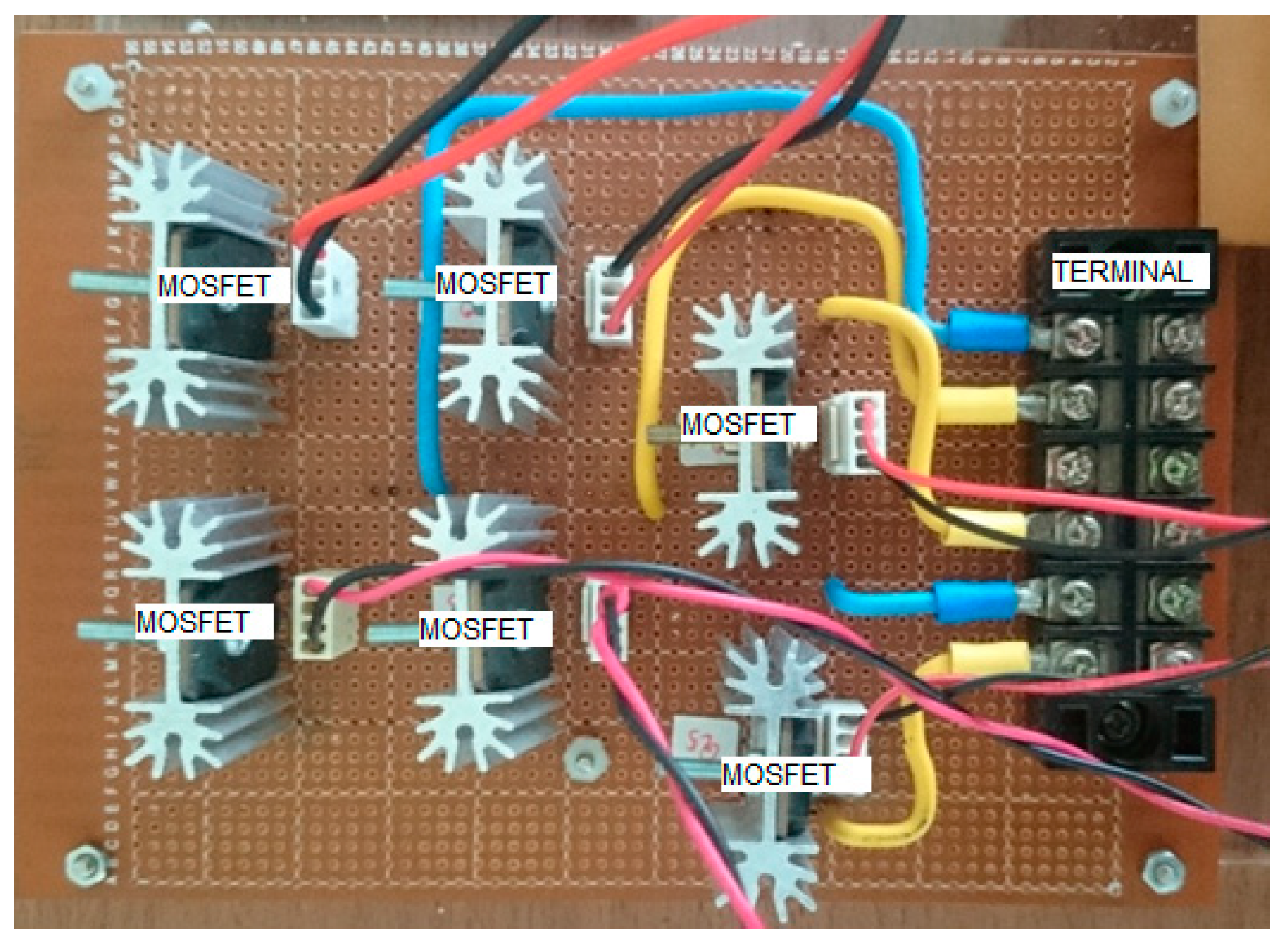
Figure 17.
Power inverter circuit using power MOSFETs.

Figure 18.
Stabilizing circuits.

Figure 19.
Dead-time circuits.

Figure 20.
Gate driver circuits.

Figure 21.
Experimental results of output voltage and load current for phase R.

Figure 22.
Measured harmonics spectrum of five-level PWM voltage therewith switching harmonics.


Table 1.
Comparison of conventional and proposed inverter circuits.
| Components | Conventional 5-Level Inverter | Proposed 5-Level Inverter |
|---|---|---|
| Controlled switch number | 24 | 18 |
| Isolated gate drive power supply | 14 | 11 |
| Driving circuits | 24 | 18 |
| DC input power | 2 | 2 or 1 |
Table 2.
Switching states of phase R voltage generation.
| Q1 | Q2 | Q3 | Q4 | Q13 | Q14 | VOut |
|---|---|---|---|---|---|---|
| ON | OFF | ON | OFF | OFF | ON | +2V |
| OFF | ON | ON | OFF | OFF | ON | +V |
| OFF | OFF | OFF | ON | OFF | ON | 0 |
| OFF | OFF | ON | OFF | ON | OFF | 0 |
| OFF | ON | OFF | ON | ON | OFF | −V |
| ON | OFF | OFF | ON | ON | OFF | −2V |
Table 3.
Experiment parameters.
| DC Input Voltage | 100 V |
| Switching frequency of power switches | 22 kHz |
| Inductor of stabilizing circuit, Lc | 100-µH |
| Modulation index | 0.975 |
| Load | R = 20 Ω, L = 5 mH |
| Basic frequency of voltage | 50 Hz |
© 2019 by the authors. Licensee MDPI, Basel, Switzerland. This article is an open access article distributed under the terms and conditions of the Creative Commons Attribution (CC BY) license (http://creativecommons.org/licenses/by/4.0/).
Share and Cite
MDPI and ACS Style
Suroso; Tri Nugroho, D.; Noguchi, T. A Different Voltage-Source Power Inverter with Carrier Based SPWM for Open-End Connection Loads. Energies 2019, 12, 3251. https://doi.org/10.3390/en12173251
AMA Style
Suroso, Tri Nugroho D, Noguchi T. A Different Voltage-Source Power Inverter with Carrier Based SPWM for Open-End Connection Loads. Energies. 2019; 12(17):3251. https://doi.org/10.3390/en12173251
Chicago/Turabian StyleSuroso, Daru Tri Nugroho, and Toshihiko Noguchi. 2019. "A Different Voltage-Source Power Inverter with Carrier Based SPWM for Open-End Connection Loads" Energies 12, no. 17: 3251. https://doi.org/10.3390/en12173251
Note that from the first issue of 2016, this journal uses article numbers instead of page numbers. See further details here.