Series-Parallel Reconfiguration Technique with Voltage Equalization Capability for Electric Double-Layer Capacitor Modules


1
College of Engineering, Ibaraki University, Hitachi 316-8511, Japan
2
Fanuc Corporation, Yamanashi 401-0597, Japan
3
Seiko Epson Corporation, Nagano 392-8502, Japan
*
Author to whom correspondence should be addressed.
Energies 2019, 12(14), 2741; https://doi.org/10.3390/en12142741
Submission received: 18 June 2019
/
Revised: 15 July 2019
/
Accepted: 16 July 2019
/
Published: 17 July 2019
(This article belongs to the Section D: Energy Storage and Application)
Abstract
:Voltage variations of electric double-layer capacitors (EDLCs) are rather wider than those of traditional rechargeable batteries, and an energy utilization ratio of EDLCs is dependent on cells’ voltage variation ranges. To satisfactorily utilize EDLCs’ energies, voltages of EDLC modules should be within a certain range, while cells need to be charged and discharged over the wide voltage range. To this end, various kinds of series-parallel reconfiguration techniques based on balance- and unbalance-shift circuits have been proposed, but conventional techniques can only be applied to modules consisting of even number cells, impairing the design flexibility and scalability. With the unbalance-shift circuits, cell voltages are unavoidably mismatched due to unequal currents, resulting in reduced energy utilization ratios. This article proposes a novel series-parallel reconfiguration technique with voltage equalization capability for EDLC modules. The proposed technique can be applied to any number of cells, improving design flexibility and scalability. Furthermore, since the proposed circuit behaves as a switched capacitor converter, in which all cells are virtually connected in parallel, cells are equally charged and discharged without causing voltage imbalance, realizing the improved energy utilization ratio. A prototype for an EDLC module comprising four cells, each with a rated charging voltage of 2.5 V, was built and experimentally tested. The module voltage varied in the range of 3.2–5.0 V, while all cells were uniformly discharged down to as low as 0.8 V, achieving the energy utilization ratio of 90%.
1. Introduction
Electric double-layer capacitors (EDLCs), also known as supercapacitors, are an energy storage device that utilizes double-layer capacitance as an energy storage mechanism. EDLCs excel over traditional rechargeable batteries in terms of power capability, cycle life, and temperature tolerance because they do not rely on chemical reactions for energy storage [1,2]. Their major drawback is that their specific energy in W/kg and energy density in W/L are rather smaller than those of rechargeable batteries. Hence, EDLCs have been chiefly used as high-power energy buffers to supplement main power sources, such as lithium-ion batteries (LIBs) and fuel cells. Lithium-ion capacitors (LICs)—a hybrid energy storage device combining the energy storage mechanisms of EDLCs and LIBs—realize higher specific energy and energy density than EDLCs [3,4,5,6,7,8,9]. EDLCs and LICs have been commercialized by various manufacturers, and some applications have started employing EDCLs and LICs as an alternative to traditional rechargeable batteries in order to achieve a longer service life and wider operation temperature range. In spacecraft power systems, for example, a feasibility study on LIC-based power systems was performed [10]. A LIC pouch cell was launched and its performance under a space environment was successfully demonstrated on orbit [9]. Another example is an uninterruptible power supply (UPS) application, where maintenance-free rechargeable energy storage devices are strongly demanded, and EDLCs have been recently used as an alternative to traditional lead-acid batteries which typically need replacement every few years.
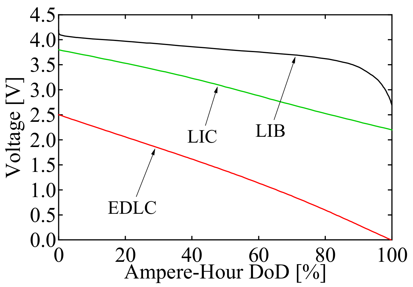
In addition to the lower energy densities, a wide voltage variation of EDLCs during cycling is often cited as a major disadvantage. Typical voltage ranges of EDLCs are 0–2.5 V, whereas those of LIBs and LICs are typically 2.7–4.2 V and 2.2–3.8 V, respectively. Typical discharging voltage profiles of an EDLC, LIB, and LIC cells as a function of ampere-hour depth-of-discharge (DoD) are compared in Figure 1.
In general, an energy utilization ratio of EDLCs, U, is expressed as:
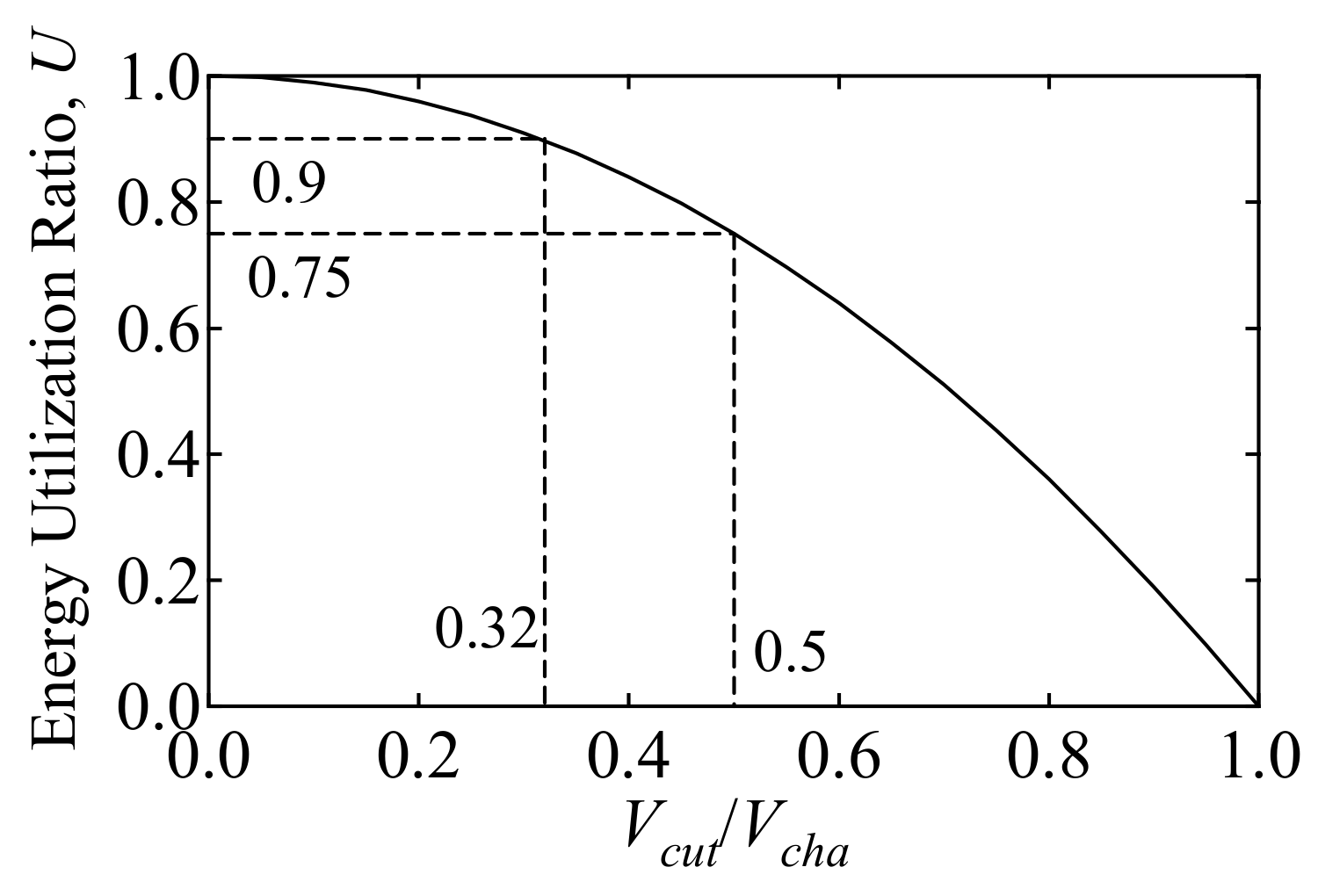
where Vcha and Vcut are the charge and cut-off voltages, respectively. Figure 2 illustrates U as a function of Vcut/Vcha. This relationship suggests that to enhance energy utilization, EDLCs need to be discharged deeply so that Vcut/Vcha is small. For examples, if EDLCs are discharged to 0.5 Vcha, 75% of the stored energy can be used. To achieve 90% energy utilization, EDLCs need to be discharged to 0.32 Vcha. However, the range of Vcut/Vcha is typically constrained by dc–dc converters that are connected in between EDLCs and loads. Poor utilization ratios are equivalent to decreased specific energies and energy densities because a certain amount of energy stored in EDLCs is unavailable and unextractable, exacerbating the drawback of EDLCs.
Various kinds of series-parallel reconfiguration techniques, or changeover circuits, have been developed to address the above issues [11,12,13,14,15,16,17]. EDLC cells together with bidirectional switches form a reconfiguration module so that series and parallel connections of cells are switched depending on cell voltages. Reconfiguration techniques can be roughly categorized into two groups: balance- and unbalance-shift circuits.
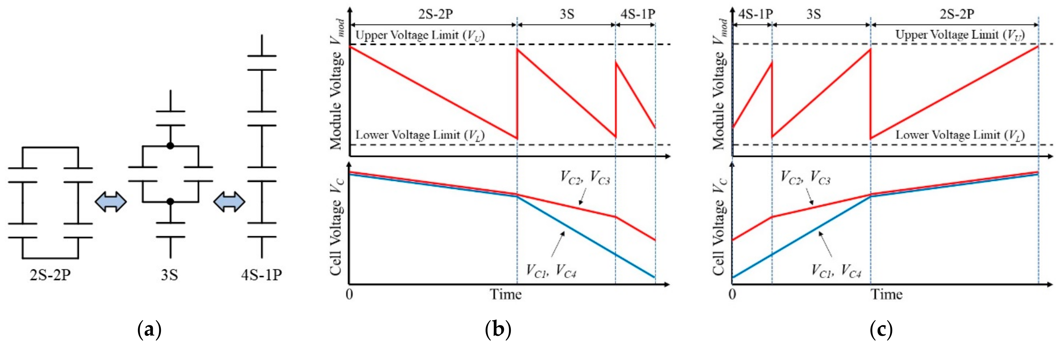
A typical reconfiguration sequence of the balance-shift circuit for four-cell module is illustrated in Figure 3a, and its discharging and charging profiles are shown in Figure 3b,c, respectively. At the beginning of discharging, all cells are connected in parallel, and hence, the module is equivalent to 1-series 4-parallel configuration (i.e., 1S-4P). After cell voltages drop to some extent, the module is reconfigured to be 2-series–2-parallel configuration (2S-2P) to double its voltage. After further discharging, all cells are connected in series (4S-1P) to lift up the module voltage again. With this reconfiguration sequence, cells can deeply discharge while the module voltage variation can be relatively small. In the charging process, the series-parallel combination is sequentially changed in reverse order. With the balance-shift circuit, all EDLC cells can be charged and discharged uniformly without producing voltage imbalance, as illustrated in the bottom panels of Figure 3b,c.
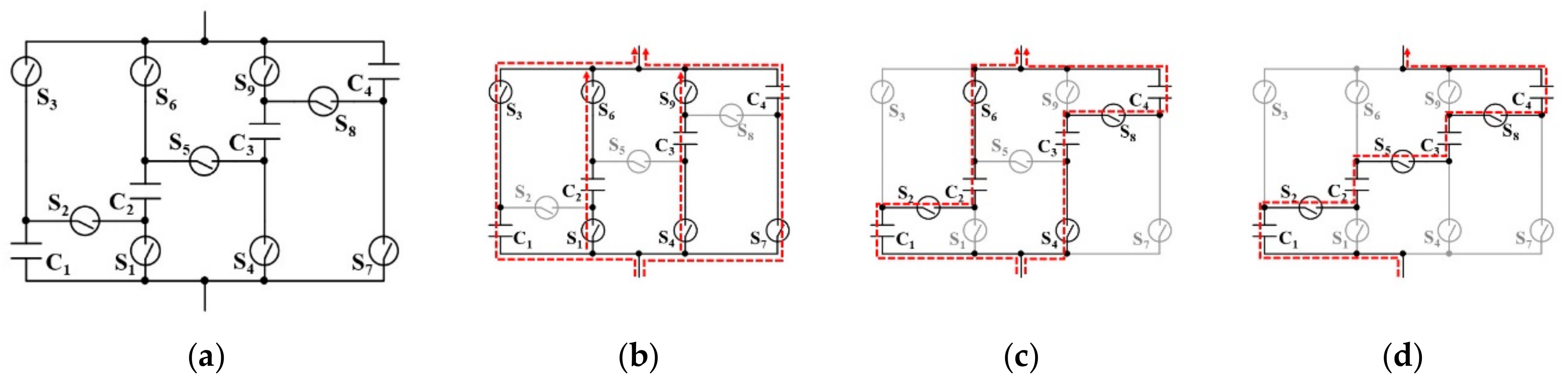
Various kinds of balance-shift circuits have been proposed [11,12,13,14,15,16], as shown in Figure 4 and Figure 5. Cells in these balance-shift circuits can be reconfigured identically to those in Figure 3, and their configurations are either 1S-4P, 2S-2P, or 4S-1P, depending on cell voltages. Although all cells can be charged and discharged uniformly with a high utilization ratio, the requirement of numerous switches is cited as a top concern. Furthermore, these techniques cannot be applied to modules consisting of odd number cells (e.g., 3, 5, and 7 cells), impairing the design flexibility and scalability.
A representative reconfiguration sequence of the unbalance-shift circuit for four cells are depicted in Figure 6a, and discharging and charging profiles of module and cell voltages are shown in Figure 6b,c, respectively. The number of series connection can be changed step by step (i.e., 2S, 3S, and 4S), realizing finer voltage step changes than balance-shift circuits. However, its major drawback is that cells are unequally charged and discharged during intermediate mode(s). In a discharging process, for example, all cells share the same discharge current in 2S-2P and 4S-1P configurations in the first and third modes, but cells in the second mode are obviously discharged unequally. This unequal current impairs the energy utilization ratio of the module as a whole because some cells might reach 0 V or, in the worst case, be over-discharged under subzero voltages.
Unbalance-shift circuits for four cells [17] and 2 m cells [16] are shown in Figure 7a,b, respectively. Reconfiguration modes during discharging are shown in Figure 7c–e. In comparison to the balance-shift circuits shown in Figure 4 and Figure 5, the switch count can be reduced, thus simplifying the circuit. However, cell voltages are naturally imbalanced due to the unequal current in the intermediate mode, as depicted in Figure 7d.
To cope with the issues of conventional reconfiguration techniques, this article presents a novel reconfiguration circuit with voltage equalization capability. The proposed reconfiguration circuit can be applied to modules consisting of any arbitrary odd and even numbered cells, realizing the improved design flexibility and scalability. In addition, cells in the proposed reconfiguration circuit can be charged and discharged without causing voltage imbalance thanks to the voltage equalization capability, hence achieving the improved energy utilization ratios. The rest of this article is organized as follows. Section 2 describes the proposed reconfiguration circuit and its major features. The operation analysis is performed in Section 3, followed by the design example in Section 4. Section 5 presents the experimental results of an EDLC module consisting of four cells.
2. Series-Parallel Reconfiguration Circuit with Voltage Equalization Capability
2.1. Circuit Description
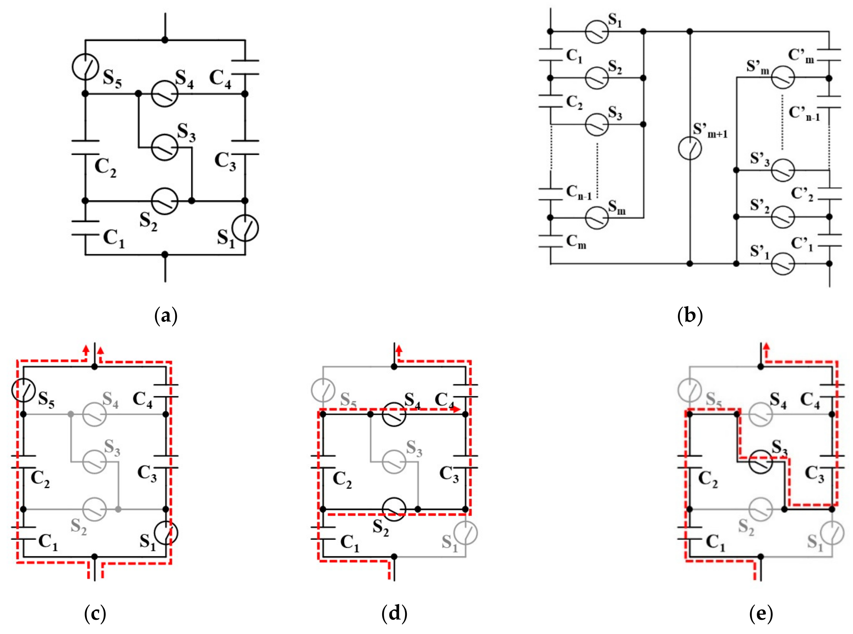
The proposed reconfiguration circuits for three cells and four cells are shown in Figure 8a,b, respectively. Series and parallel connections of cells are reconfigured by switches. Diodes are connected in parallel with switches in order to provide current flow paths during dead time periods (detailed in Section 3).
The proposed reconfiguration technique can be applied to any arbitrary odd and even numbered cells. The proposed reconfiguration circuit for n cells is depicted in Figure 8c. The number of cells can be arbitrarily extended by adding two switches for every cell. The cell count n can be any integer, including odd numbers.
The configuration of the circuit for three cells (Figure 8a) in a discharging process is switched in the order of 2S and 3S-1P. All cells uniformly discharge in series in the 3S-1P configuration, and therefore no voltage imbalance occurs. In the 2S configuration, on the other hand, cells are discharged with different current rates and their voltages tend to be imbalanced. To equalize the cell voltages, the series-parallel connection of these three cells are sequentially changed. Similarly, the series-parallel configuration of the module for four cells (Figure 8b) in a discharging process is changed in the order of 2S-2P, 3S, and 4S-1P. Cells uniformly discharge in the 2S-2P and 4S-1P configurations, whereas those in the 3S configuration are discharged unequally. Therefore, the series-parallel connections of four cells are repeatedly changed in order to preclude voltage imbalance in the 3S configuration. In Section 3, operations of a module for four cells in discharging and charging processes is explained.
2.2. Major Features
As mentioned in Section 2.1, the proposed reconfiguration circuit can be applied to any number of cells, hence improving the design flexibility and scalability in comparison to conventional circuits, which can only be applied to even numbered cells, as mentioned in Section 1. In addition, the switch count can be reduced in comparison with balance-shift circuits, realizing a simplified circuit.
As will be detailed in Section 3, the proposed reconfiguration circuit behaves as a switched capacitor converter [18,19,20,21], in which all cells are virtually connected in parallel and their voltages are automatically balanced, and therefore, all cells can be charged and discharged uniformly. In other words, all cells are utilized equally, realizing an improved utilization ratio of the module compared to the conventional unbalance-shift circuit shown in Figure 7.
The proposed series-parallel reconfiguration circuit is compared to conventional balance- and unbalance-shift circuits in terms of the switch count, the applicable number of cells, and voltage balance capability, as shown in Table 1 where n (≥2) is the number of cells in a module. Cells in the balance-shift circuit can be charged and discharged equally, but its switch count is prone to be larger than other circuits. The unbalance-shift circuit requires the fewest switch count, but it suffers from voltage imbalance, as illustrated in Figure 6. Both conventional circuits are applicable to only even numbered cells (e.g., 4, 6, 8…), hence impairing the design flexibility and scalability. Meanwhile, the proposed reconfiguration circuit can be applied to any number of cells, and therefore, the modules can be flexibly designed and scaled up to be larger systems. Furthermore, all cells in the proposed reconfiguration circuit can be charged and discharged equally without causing voltage imbalance, achieving higher energy utilization than the conventional unbalance-shift circuit.
According to previous work on reconfiguration circuits [11,16], the larger the number of stages or cells n, the better will be the energy utilization ratio U. However, the circuit complexity is prone to soar due to the increased switch count. Therefore, reconfiguration techniques have generally been employed for modules consisting of around four cells—for large-scale systems, reconfiguration techniques are applied at a module-level, not a cell-level (i.e., C1–C4 in figures in Section 1 are a module, not a cell). This tendency is also true for the proposed reconfiguration technique, and therefore, the circuit for four cells is explained and discussed in the following sections.
3. Operation Analysis
Depending on cell voltages, the series-parallel configuration of the proposed circuit is sequentially changed, similarly to conventional reconfiguration circuits. However, in intermediate modes, the proposed circuit behaves as a switched capacitor converter [18,19,20,21], and all cell voltages are balanced, realizing uniform cell utilization. This section deals with the circuit for four cells, but operations of a circuit for n cells can also be explained similarly.
3.1. Voltage Profiles and Mode Transitions
Theoretical voltage profiles in discharging and charging modes are shown in Figure 9a,b, respectively. The proposed reconfiguration circuit for four cells operates chiefly with three modes, Modes 1–3, and Mode 2 consists of three sub-modes, sub-Modes A–C. These modes and sub-modes are sequentially shifted with inserting a dead time period in order to prevent excessive large currents due to possible short-circuit paths.
The mode transition map is depicted in Figure 10. In a discharging process, the proposed reconfiguration circuit operates in the order of Mode 1, 2, and 3. At a moment of the mode transition from Mode 1 to 2, any sub-modes in Mode 2 can be directly reached from Mode 1 via a dead time period. In Mode 2, sub-Modes A–C are periodically switched in order to prevent voltage imbalance or to equalize cell voltages. At a moment of the mode transition from Mode 2 to 3, the operation can shift to Mode 3 from any sub-modes in Mode 2. In a charging process, on the other hand, the operation shifts in the order of Mode 3, 2, and 1, but the fundamental operating principle is identical to that in the discharging process.
3.2. Operation in Discharging Mode
Voltage profiles and operation modes in the discharging process are shown in Figure 9a and Figure 11, respectively. As described in the previous subsection and in Figure 10, there are three ways to/from sub-modes in Mode 2. In this subsection, the mode transitions from Mode 1 to sub-Mode A and from sub-Mode C to Mode 3 are taken as example cases to be explained.
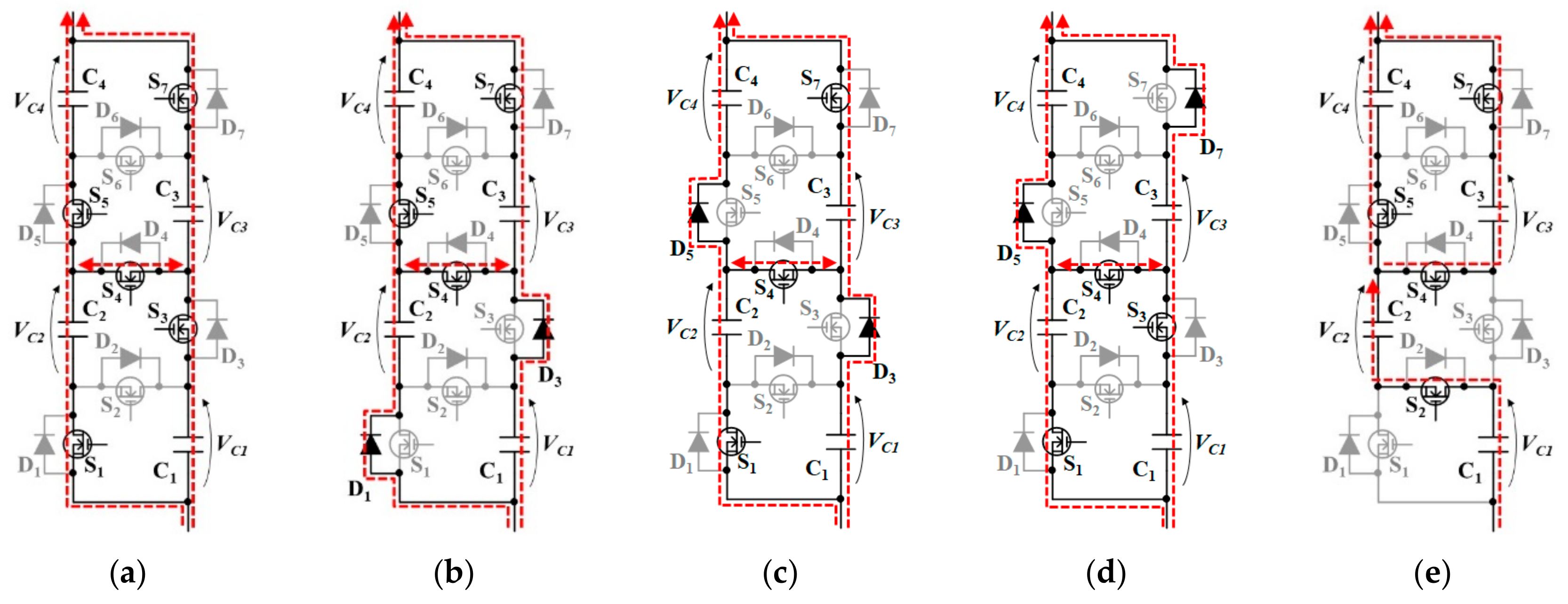
Mode 1 (Figure 11a): S1, S3, S4, S5, and S7 are on. The reconfiguration circuit is equivalent to 2S-2P. C1 and C2 are connected in parallel, and so are C3 and C4. The module voltage, Vmod, at the beginning of this mode is equal to 2Vcha (Vcha being the charge voltage of cells). Voltages of parallel-connected cells are naturally balanced. Vmod as well as cell voltages VC decreases, and all cells are equally discharged unless the total capacitance of C1 and C2 severely differs from that of C3 and C4. At the end of Mode 1, VC and Vmod decrease to VM1 and 2VM1 (VM1 being the cell voltage at the end of Mode 1), respectively.
Dead Time between Mode 1 and Sub-Mode A (Figure 11b): S1 and S3 are turned off, and D1 and D3 start conducting. Meanwhile, S4, S5, and S7 are still on. The module configuration is still 2S-2P.
Sub-Mode A in Mode 2 (Figure 11e): S4, S5, and S7 are still on, whereas S2 is turned on so as to reconfigure the circuit to be 3S. C1 and C2 are in series through S2, and hence, the module voltage Vmod jumps to as high as 3VM1 at the beginning of Mode 2. C3 and C4 are connected in parallel, and their voltages are balanced.
Dead Time between Sub-Modes A and B (Figure 11f): S4 and S7 are turned off while S2 and S5 are still on. Although C3 does not contribute to discharging, the module configuration is still 3S.
Sub-Mode B in Mode 2 (Figure 11g): S3 and S6 are turned on, and C2 and C3 are connected in parallel. The module configuration is 3S, and voltages of C2 and C3 are naturally balanced in this sub-mode.
Dead Time between Sub-Modes B and C (Figure 11h): S3 and S6 are kept on, while S2 and S5 are turned off. Although C2 does not contribute to discharging, the module configuration is still 3S.
Sub-Mode C in Mode 2 (Figure 11i): S1 and S4 are turned on so as to connect C1 and C2 in parallel. The module configuration is 3S, and voltages of C1 and C2 are naturally balanced.
By repeating sub-Modes A–C with inserting dead time periods, all cells are virtually connected in parallel and their voltages are automatically balanced in Mode 2. Meanwhile, the module configuration can be maintained to be 3S, even though series-parallel connections are sequentially changed. At the end of Mode 2, VC and Vmod decrease to VM2 and 3VM2 (VM2 being the cell voltage at the end of Mode 2), respectively.
Dead Time between Sub-Mode C and Mode 3 (Figure 11l): S1 and S3 are turned off, and D1 and D3 conduct. Meanwhile, S4 and S6 are still on. The configuration is still 3S.
Mode 3 (Figure 11m): S2 is turned on, and all cells are connected in series, forming the 4S-1P configuration. Vmod jumps to 4VM2. All cells uniformly discharge in series, and no voltage imbalance occurs unless capacitances are severely mismatched. VC declines to VM3 at the end of Mode 3.
In summary, module configurations in Modes 1 and 3 are identical to those in the conventional circuits shown in Figure 7. In Mode 2, all cells are virtually connected in parallel thanks to the switched capacitor operation throughout sub-Modes A–C.
3.3. Operation in Charging Mode
Voltage profiles and operation modes in the charging process are shown in Figure 9b and Figure 12, respectively. The proposed reconfiguration circuit in the charging process operates in a similar manner to the discharging process. In this subsection, mode transitions from Mode 3 to sub-Mode C and from sub-Mode A to Mode 1 are discussed.
Mode 3 (Figure 12a): S2, S4, and S6 are on, and the circuit is equivalent to 4S-1P. All cells are charged uniformly as long as cell capacitances are matched satisfactorily. VC and Vmod reach VM2 and 4VM2 at the end of Mode 3.
Dead Time between Mode 3 and Sub-Mode C (Figure 12d): S2 is turned off, and its anti-parallel diode D2 conducts instead. The configuration is still 4S-1P.
Sub-Mode C in Mode 2 (Figure 12i): S1 and S3 are turned on to connect C1 and C2 in parallel. The module configuration is 3S, and therefore, Vmod falls down to 3VM2. Voltages of C1 and C2 are balanced as these cells are connected in parallel.
Dead Time between Sub-Modes C and B (Figure 12h): S3 and S6 are still on, whereas S1 and S4 are turned off. Although C2 is not being charged in this sub-mode, the module is still 3S configuration.
Sub-Mode B in Mode 2 (Figure 12g): S2 and S5 are turned on while S3 and S6 are kept on. C2 and C3 are connected in parallel, and their voltages are unified. The module configuration is still 3S.
Dead Time between Sub-Modes B and A (Figure 12f): S3 and S6 are turned off. Although C3 is isolated from the charging path, the module configuration is still 3S.
Sub-Mode A in Mode 2 (Figure 12e): S4 and S7 are turned off so as to connect C3 and C4 in parallel. Voltages of C3 and C4 are balanced thanks to the parallel connection.
In Mode 2, sub-Modes A–C are repeatedly changed so that all the cell voltages are balanced. Meanwhile, the module configuration is kept 3S even in the dead time periods. The sub-mode transitions in Mode 2 are repeated until VC and Vmod reach VM1 and 3VM1, respectively.
Dead Time between Sub-Mode A and Mode 1 (Figure 12j): S2 is turned off while S4, S5, and S7 are still on. The anti-parallel diode D2 starts conducting instead of S2.
Mode 1 (Figure 12m): S5 and S7 are turned on so as to connect C1 and C2 in parallel. The module is in 2S-2P configuration, and therefore, Vmod drops to 2VM1 at the beginning of Mode 1. Voltages of parallel-connected cells are balanced automatically, and all cell voltages are uniform unless there is huge capacitance mismatch.
3.4. Operation Conditions
The series-parallel connection in the proposed circuit must be reconfigured so that Vmod be within the upper and lower voltage limits of VU and VL. From the profile of Vmod in Figure 9a, following sets of equations can be yielded:
where T1–T3 are the time at the end of Modes 1–3 in the discharging mode. Rearrangement of Equations (2) and (3) produces:
VM1 and VM2 must be determined to fulfill Equations (4) and (5). The relationship between VU and VL can be yielded from Equations (4) and (5), as:
3.5. Reconfiguration Algorithm
Assuming all cell voltages are equalized to be VC, the module configuration is determined based on VC, as:
The flowchart of the reconfiguration sequence for the four-cell module is depicted in Figure 13. Series-parallel configuration or Modes 1–3 are switched based on the value of VC. Meanwhile, sub-modes in Mode 2 are sequentially changed at a low frequency (e.g., 4 Hz in the experimental test, Section 4).
In Modes 1 and 3, all cells are essentially charged/discharged uniformly as the series-parallel configurations of cells are fixed. In Mode 2, the series-parallel configuration is sequentially switched, as illustrated in Figure 11 and Figure 12, and cell voltages are equalized by virtually connecting all cells in parallel. However, in each sub-mode, cell voltages slightly deviate due to nonuniform charge/discharge currents. For example, C1 and C2 in sub-Mode C (Figure 11i) are in parallel and are discharged uniformly, but a discharging current of C1 in other sub-modes and dead time periods is twice that of C2. Voltages of C1 and C2 are slightly imbalanced, and they are connected in parallel again when the operation comes back to sub-Mode C. This voltage imbalance might result in an excessively large current at the moment of the mode transition. Therefore, the voltage imbalance generated in Mode 2 should be low enough by changing sub-modes frequently.
A voltage imbalance between C1 and C2 generated in Mode 2 is focused here as an example, but a voltage imbalance between C3 and C4 can be analyzed identically. Sub-mode lengths as well as dead time periods are assumed equal to be TS. From sub-Mode C as an origin, it takes 7TS for the operation to come back to sub-Mode C again (see Figure 10). C1 and C2 are discharged with Imod and Imod/2 (Imod being the module current), respectively, in sub-Modes A and B. The voltage imbalance generated before the operation comes back to sub-Mode C is given by:
where C is the cell capacitance. This equation suggests TS should be properly determined depending on values of Imod and C so that ΔV is low enough. In general, Imod/C for high-power applications (e.g., 20C rate) is around 0.014—Q = CV = IT with V = 2.5 and T = 180 sec (=3600/20) yields I/C ≈ 0.014. Assume TS = 0.25 (i.e., 4 Hz), ΔV can be as low as 12 mV that is considered low enough to preclude excessive large current in parallel connection.
4. Design Example
A reconfiguration circuit for four cells, each with a capacitance of 400 F at a rated charging voltage Vcha = 2.5 V, with Imod of 0.4 A is assumed and key parameters of VU, VL, VM1, and VM2 are determined to achieve 90% utilization ratio. Although VU, VL, VM1, and VM2 can be an arbitrary value in a certain range, the lowest possible values are chosen in this article.
According to Equation (1) and Figure 2, Vcut is determined to be 0.8 V to achieve 90% energy utilization, and hence, VM3 = 0.8 V. Applying Vcha = 2.5 V and VM3 = 0.8 V into Equations (2) and (3) yields VU ≥ 5.0 V and VL ≥ 3.2 V. The lowest values of VU = 5.0 V and VL = 3.2 V are chosen here, and these values satisfy Equation (6). Substitution of VU = 5.0 V and VL = 3.2 V into Equations (4) and (5) produces 1.66 V ≥ VM1 ≥ 1.60 V and 1.25 V ≥ VM2 ≥ 1.07 V, respectively. Accordingly, VM1 and VM2 are determined to be 1.60 V and 1.07 V, respectively.
5. Experimental Results
A prototype for a four-cell module was built and tested to verify the proposed reconfiguration concept. EDLCs with a capacitance of 400 F at a rated charge voltage of 2.5 V were used. The module was discharged and charged with a constant current of 0.4 A. VM1 and VM2 were set to be 1.60 V and 1.07 V, respectively, as determined in Section 4. An average cell voltage was used as VC for the reconfiguration control. The switching frequency in Mode 2 was 4 Hz.
The resultant discharging and charging profiles are shown in Figure 14. In the discharging mode, cells in Mode 1 were discharged with a slight voltage imbalance due to a minor initial voltage mismatch. When VC reached 1.60 V, the module was reconfigured to be 3S in Mode 2, and Vmod rose. All cell voltages in Mode 2 were unified, and the initial voltage mismatch found in Mode 1 vanished thanks to the switched capacitor operation. The module was reconfigured to be 4S-1P when VC dropped to 1.07 V, and all cells were eventually discharged as low as 0.8 V at the end of Mode 3. In the charging process (see Figure 14b), the module was reconfigured in reverse order. All cells were eventually charged to 2.5 V without causing voltage imbalance.
The resultant discharging and charging profiles agreed very well with the theoretical ones shown in Figure 9, demonstrating the proposed reconfiguration technique. The module voltage variation was limited between 3.2 V and 5.0 V, while cells were cycled in the range of 0.8–2.5 V, achieving the energy utilization ratio of 90%.
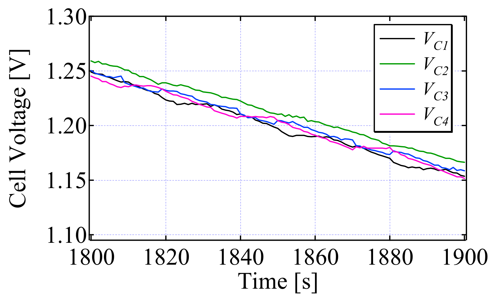
Cell voltages in Mode 2 in the discharging mode are zoomed in Figure 15. All the cell voltages were equalized well, demonstrating the equalization performance of the proposed series-parallel reconfiguration circuit.
6. Conclusions
The series-parallel reconfiguration circuit with voltage equalization capability has been proposed for EDLC modules in this paper. In comparison with conventional balance-shift circuits, not only can the switch count be reduced but also the proposed reconfiguration circuit can be applied to any arbitrary odd and even number of cells, improving the design flexibility and scalability. In addition, since the proposed circuit behaves as a switched capacitor converter, with which all cells are virtually connected in parallel, all cells can be charged and discharged uniformly, realizing the improved utilization ratio of the module compared to the conventional unbalance-shift circuits.
In this study, a prototype for an EDLC module comprising four cells, each with a rated charging voltage of 2.5 V, was built and tested. The experimental discharging and charging profiles agreed very well with theoretical ones, verifying the proposed concept. The module voltage in the experiment varied between 3.2 V and 5.0 V while all cells in the module were cycled in the range of 0.8–2.5 V, achieving the energy utilization ratio of 90%.
Author Contributions
Conceptualization, M.U.; methodology, M.U.; simulation analysis, I.K. and H.K.; validation, I.K. and H.K.; writing—original draft preparation, M.U.; writing—review and editing, M.U.; supervision, M.U. and H.K.
Funding
This research received no external funding.
Conflicts of Interest
The authors declare no conflict of interest.
References
- Uno, M.; Tanaka, K. Accelerated charge-discharge cycling test and cycle life prediction model for supercapacitors in alternative battery applications. IEEE Trans. Ind. Electron. 2012, 59, 4704–4712. [Google Scholar] [CrossRef]
- Carbone, R. Energy Storage in the Emerging Era of Smart Grids; InTech: London, UK, 2011; pp. 21–40. ISBN 978-953-307-269-2. [Google Scholar]
- Gualous, H.; Alcicek, G.; Diab, Y.; Hammar, A.; Venet, P.; Adams, K.; Akiyama, M.; Marumo, C. Lithium ion capacitor characterization and modeling. In Proceedings of the ESSCAP’2008, Rome, Italy, 6–7 November 2008; pp. 1–4. [Google Scholar]
- Lambert, S.M.; Pickert, V.; Holden, J.; He, X.; Li, W. Comparison of supercapacitor and lithium-ion capacitor technologies for power electronics applications. In Proceedings of the Power Electronics Machines and Drives, Brighton, UK, 19–21 April 2010; pp. 1–5. [Google Scholar]
- Böckenfeld, N.; Kühnel, R.S.; Passerini, S.; Winter, M.; Balducci, A. Composite LiFePO4/AC high rate performance electrodes for Li-ion capacitors. J. Power Sources 2011, 196, 4136–4142. [Google Scholar] [CrossRef]
- Omar, N.; Daowd, M.; Hegazy, O.; Sakka, M.A.; Choosemans, T.; Bossche, P.V.D.; Mierlo, J.V. Assessment of lithium-ion capacitor for using in battery electric vehicle and hybrid electric vehicle applications. Electrochem. Acta 2012, 86, 305–315. [Google Scholar] [CrossRef]
- Omar, N.; Sakka, M.A.; Mierlo, J.V.; Bossche, P.V.; Gualous, H. Electric and thermal characterization of advanced hybrid Li-ion capacitor rechargeable energy storage system. In Proceedings of the Power Engineering Energy Electrical Drives (POWERENG), Istanbul, Turkey, 13–17 May 2013; pp. 1574–1580. [Google Scholar]
- Uno, M.; Kukita, A. Cycle life evaluation based on accelerated aging testing for lithium-ion capacitors as alternative to rechargeable batteries. IEEE Trans. Ind. Appl. 2016, 63, 1607–1617. [Google Scholar] [CrossRef]
- Zoran, S. Supercapacitor Design and Applications; InTech: London, UK, 2016; pp. 121–143. ISBN 978-953-51-2749-9. [Google Scholar]
- Uno, M.; Tanaka, K. Spacecraft electrical power system using lithium-ion capacitors. IEEE Trans. Aerosp. Electron. Syst. 2013, 49, 175–188. [Google Scholar] [CrossRef]
- Monthéard, R.; Bafleur1, M.; Boitier, V.; Dilhac, J.M.; Lafontan, X. Self-adaptive switched ultra-capacitors: A new concept for efficient energy harvesting and storage. In Proceedings of the Power MEMS 2012, Atlanta, GA, USA, 2–5 December 2012; pp. 283–286. [Google Scholar]
- Kim, Y.; Park, S.; Wang, Y.; Xie, Q.; Chang, N.; Poncino, M.; Pedram, M. Balanced reconfiguration of storage banks in a hybrid electrical energy storage system. In Proceedings of the IEEE/ACM International Conference Computer-Aided Design (ICCAD), San Jose, CA, USA, 7–10 November 2011; pp. 624–631. [Google Scholar]
- Monteiro, J.; Garrido, N. An experimental study of an efficient supercapacitor stacking scheme to power mobile phones. In Proceedings of the IEEE 33rd International Telecommunications Energy Conference (INTELEC), Amsterdam, The Netherlands, 9–13 October 2011; pp. 1–5. [Google Scholar]
- Mahboubi, F.E.; Bafleur, M.; Boitier, V.; Alvarez, A.; Colomer, J.; Miribel, P.; Dilhac, J.M. Self-powered adaptive switched architecture storage. In Proceedings of the Power MEMS 2016, Paris, France, 6–9 December 2016; pp. 1–4. [Google Scholar]
- Uno, M. Series-parallel reconfiguration technique for supercapacitor energy storage systems. In Proceedings of the the IEEE Region Ten Conference (TENCON), Singapore, 23–26 January 2009; pp. 1–5. [Google Scholar]
- Fang, X.; Kutkut, N.; Shen, J.; Batarseh, I. Analysis of generalized parallel-series ultracapacitor shift circuits for energy storage systems. Renew. Energy 2011, 36, 2599–2604. [Google Scholar] [CrossRef]
- Sugimoto, S.; Ogawa, S.; Katsukawa, H.; Mizutani, H.; Okamura, M. A study of series-parallel changeover circuit of a capacitor bank for an energy storage system utilizing electric double layer capacitors. Electr. Eng. Jpn. 2003, 145, 33–42. [Google Scholar] [CrossRef]
- Baughman, A.; Ferdowsi, M. Double-tiered switched-capacitor battery charge equalization technique. IEEE Trans. Ind. Appl. 2008, 55, 2277–2285. [Google Scholar] [CrossRef]
- Uno, M.; Tanaka, K. Influence of high-frequency charge-discharge cycling induced by cell voltage equalizers on the life performance of lithium-ion cells. IEEE Trans. Veh. Technol. 2011, 60, 1505–1515. [Google Scholar] [CrossRef]
- Kim, M.Y.; Kim, C.H.; Kim, J.H.; Moon, G.W. A chain structure of switched capacitor for improved cell balancing speed of lithium-ion batteries. IEEE Trans. Ind. Electron. 2014, 61, 3989–3999. [Google Scholar] [CrossRef]
- Uno, M.; Akio, K. PWM converter integrating switched capacitor converter and series-resonant voltage multiplier as equalizers for photovoltaic modules and series-connected energy storage cells for exploration rovers. IEEE Trans. Power Electron. 2017, 32, 8500–8513. [Google Scholar] [CrossRef]
Figure 1.
Voltage variations of lithium-ion battery (LIB), lithium-ion capacitor (LIC), and electric double-layer capacitor (EDLC) cells as a function of ampere-hour DoD.
Figure 1.
Voltage variations of lithium-ion battery (LIB), lithium-ion capacitor (LIC), and electric double-layer capacitor (EDLC) cells as a function of ampere-hour DoD.

Figure 2.
Energy utilization ratio of EDLC as a function of ratio of cut-off voltage to charge voltage (Vcut/Vcha).
Figure 2.
Energy utilization ratio of EDLC as a function of ratio of cut-off voltage to charge voltage (Vcut/Vcha).

Figure 3.
(a) Typical reconfiguration sequence of balance-shift circuit for four-cell module, (b) its discharging, and (c) charging profiles.
Figure 3.
(a) Typical reconfiguration sequence of balance-shift circuit for four-cell module, (b) its discharging, and (c) charging profiles.
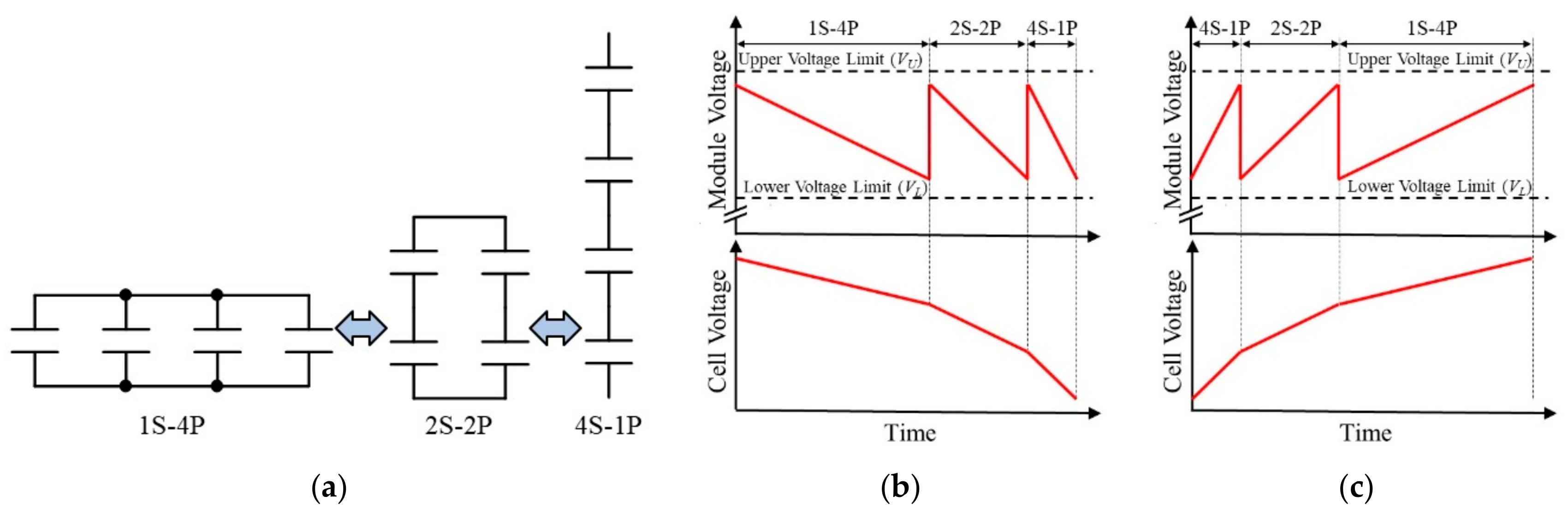
Figure 4.
(a) Balance-shift circuit, (b) 1-series 4-parallel (1S-4P), (c) 2S-SP, and (d) 4S-1P.
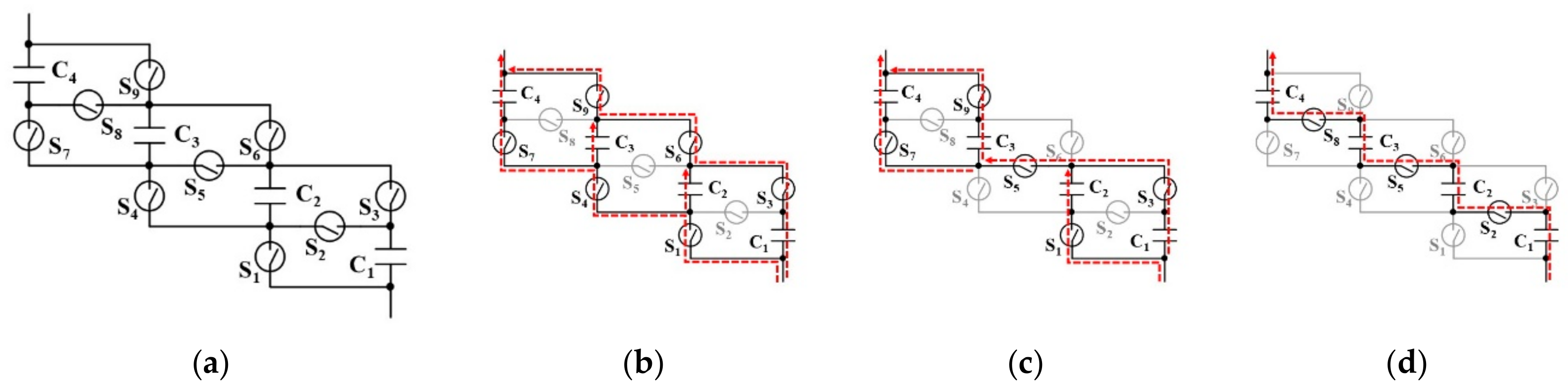
Figure 5.
(a) Balance-shift circuit, (b) 1S-4P, (c) 2S-2P, and (d) 4S-1P.

Figure 6.
(a) Typical reconfiguration sequence of unbalance-shift circuit for four-cell module, (b) its discharging, and (c) charging profiles.
Figure 6.
(a) Typical reconfiguration sequence of unbalance-shift circuit for four-cell module, (b) its discharging, and (c) charging profiles.

Figure 7.
Unbalance-shift circuit for (a) four cells and (b) 2 m cells. Operation modes of unbalance-shift circuit for four cells; (c) 2S-2P, (d) 3S, and (e) 4S-1P.
Figure 7.
Unbalance-shift circuit for (a) four cells and (b) 2 m cells. Operation modes of unbalance-shift circuit for four cells; (c) 2S-2P, (d) 3S, and (e) 4S-1P.

Figure 8.
Proposed series-parallel reconfiguration module for (a) three cells, (b) four cells, and (c) n cells.
Figure 8.
Proposed series-parallel reconfiguration module for (a) three cells, (b) four cells, and (c) n cells.
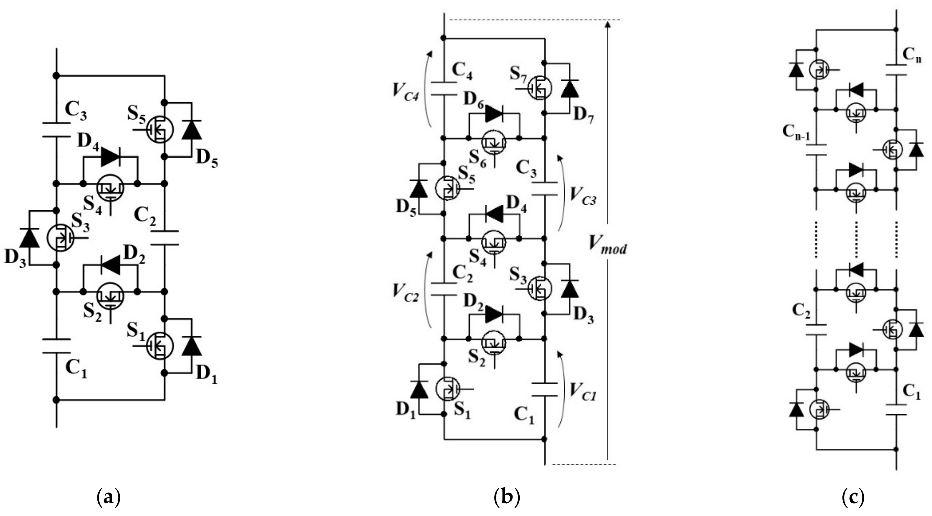
Figure 9.
Module voltage Vmod and cell voltage VC in (a) discharging and (b) charging.

Figure 10.
Mode transition map.

Figure 11.
Mode transitions in the discharging process: Current flow paths in (a) Mode 1, (b) dead time between Mode 1 and sub-Mode A, (c) dead time between Mode 1 and sub-Mode B, (d) dead time between Mode 1 and sub-Mode C, (e) sub-Mode A, (f) dead time between sub-Modes A and B, (g) sub-Mode B, (h) dead time between sub-Modes B and C, (i) Mode C, (j) dead time between sub-Mode A and Mode 3, (k) dead time between sub-Mode B and Mode 3, (l) dead time between sub-Mode C and Mode 3, and (m) Mode 3.

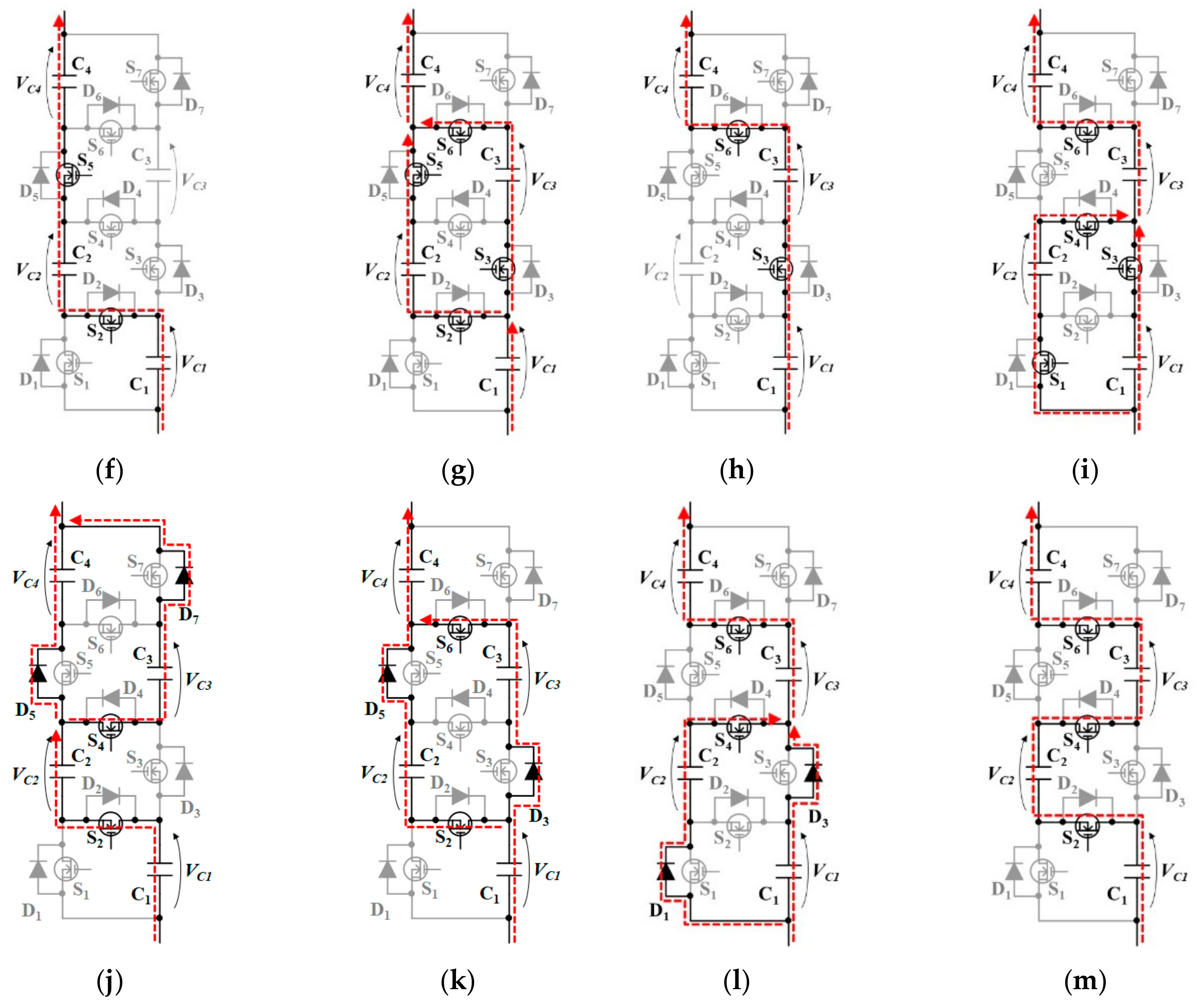
Figure 12.
Mode transitions in charging process: current flow paths in (a) Mode 3, (b) dead time between Mode 3 and sub-Mode A, (c) dead time between Mode 3 and sub-Mode B, (d) dead time between Mode 3 and sub-Mode C, (e) sub-Mode A, (f) dead time between sub-Modes A and B, (g) sub-Mode B, (h) dead time between sub-Modes B and C, (i) Mode C, (j) dead time between sub-Mode A and Mode 1, (k) dead time between sub-Mode B and Mode 1, (l) dead time between sub-Mode C, and Mode 1 (m) Mode 1.
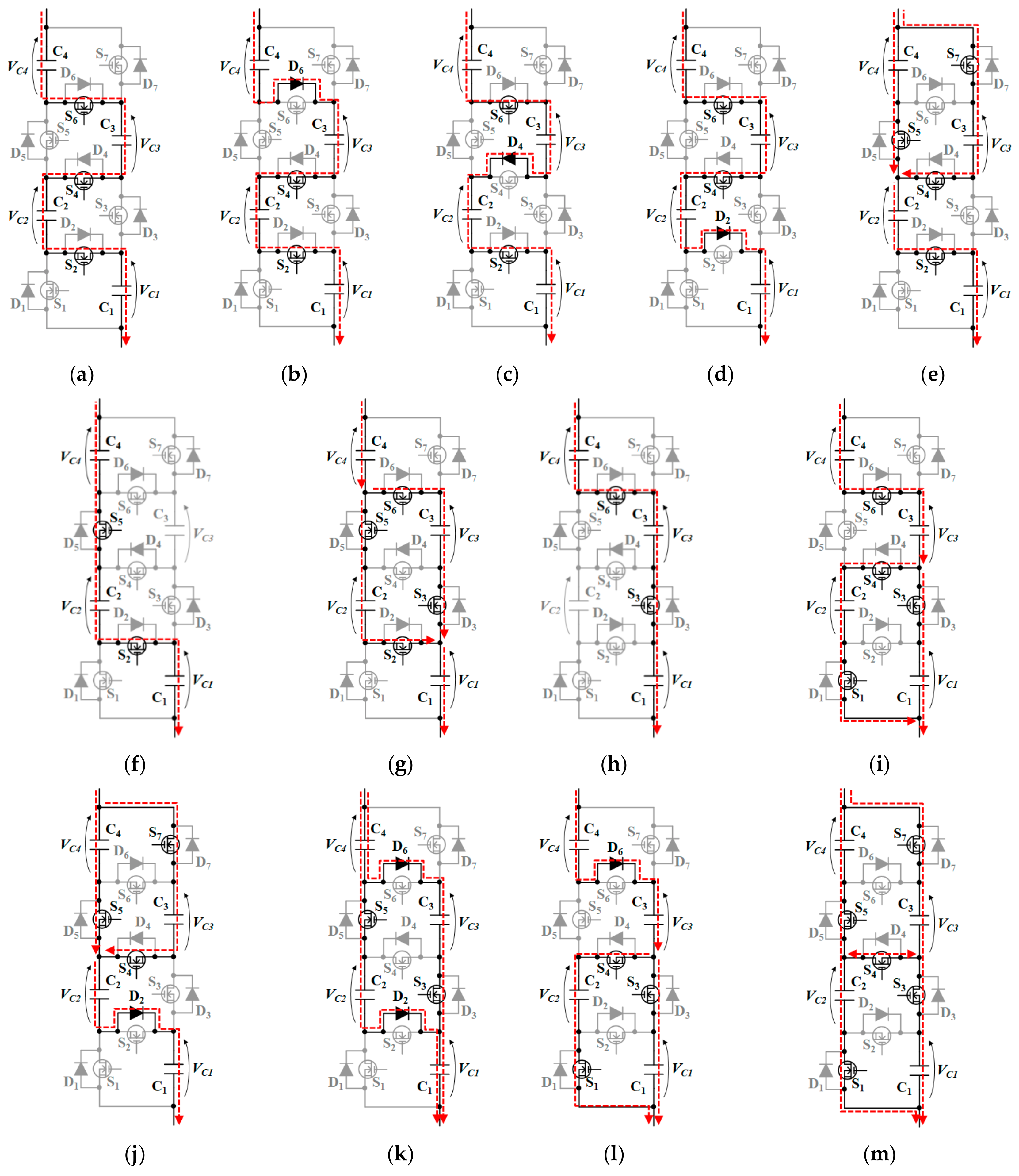
Figure 13.
Flowchart of reconfiguration sequence.

Figure 14.
Experimental results. (a) Discharging profiles and (b) charging profiles.

Figure 15.
Zoomed cell voltage profiles in Mode 2 in discharging process.

Table 1.
Comparison among conventional and proposed reconfiguration circuits.
| Topology | Balance-Shift Circuit | Unbalance-Shift Circuit | Proposed |
|---|---|---|---|
| Switch Count | 3(n − 1) | n + 1 | 2n − 1 |
| Applicable Cell Number | Even Number | Even Number | Any Number Cells |
| Voltage Balance | Balanced | Unbalanced | Balanced |
© 2019 by the authors. Licensee MDPI, Basel, Switzerland. This article is an open access article distributed under the terms and conditions of the Creative Commons Attribution (CC BY) license (http://creativecommons.org/licenses/by/4.0/).
Share and Cite
MDPI and ACS Style
Uno, M.; Iwasaki, K.; Hasegawa, K. Series-Parallel Reconfiguration Technique with Voltage Equalization Capability for Electric Double-Layer Capacitor Modules. Energies 2019, 12, 2741. https://doi.org/10.3390/en12142741
AMA Style
Uno M, Iwasaki K, Hasegawa K. Series-Parallel Reconfiguration Technique with Voltage Equalization Capability for Electric Double-Layer Capacitor Modules. Energies. 2019; 12(14):2741. https://doi.org/10.3390/en12142741
Chicago/Turabian StyleUno, Masatoshi, Koyo Iwasaki, and Koki Hasegawa. 2019. "Series-Parallel Reconfiguration Technique with Voltage Equalization Capability for Electric Double-Layer Capacitor Modules" Energies 12, no. 14: 2741. https://doi.org/10.3390/en12142741
Note that from the first issue of 2016, this journal uses article numbers instead of page numbers. See further details here.