Metal/Semiconductor Barrier Properties of Non-Recessed Ti/Al/Ti and Ta/Al/Ta Ohmic Contacts on AlGaN/GaN Heterostructures


 , , , and
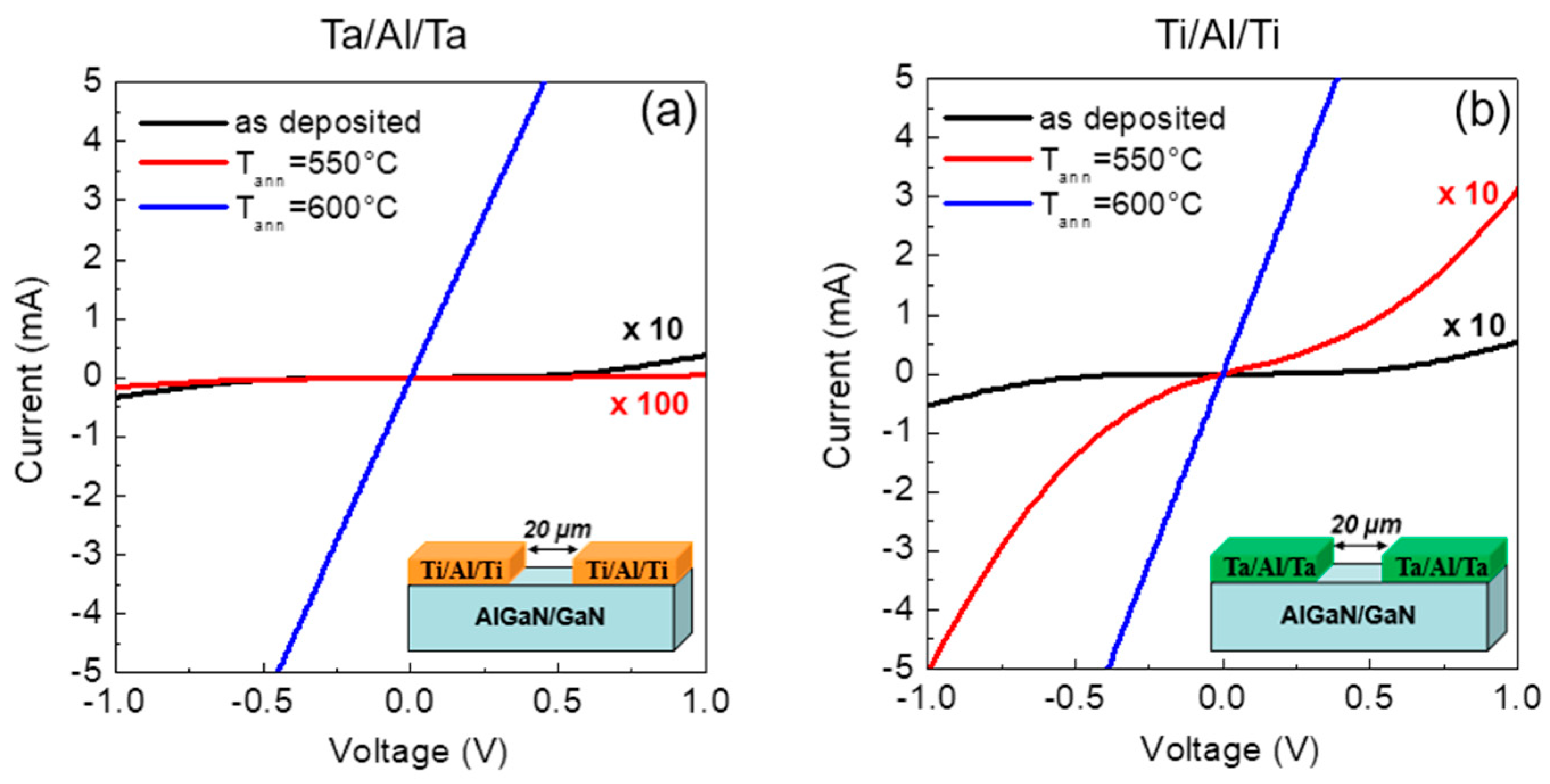
Abstract
:1. Introduction
2. Materials and Methods
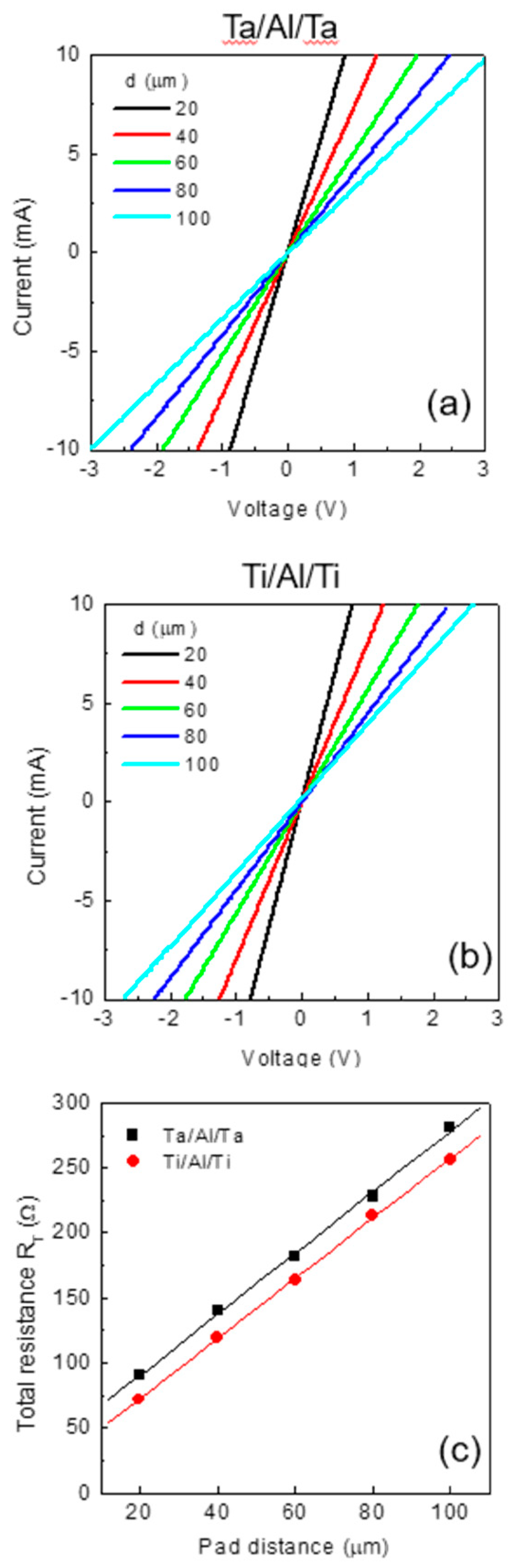
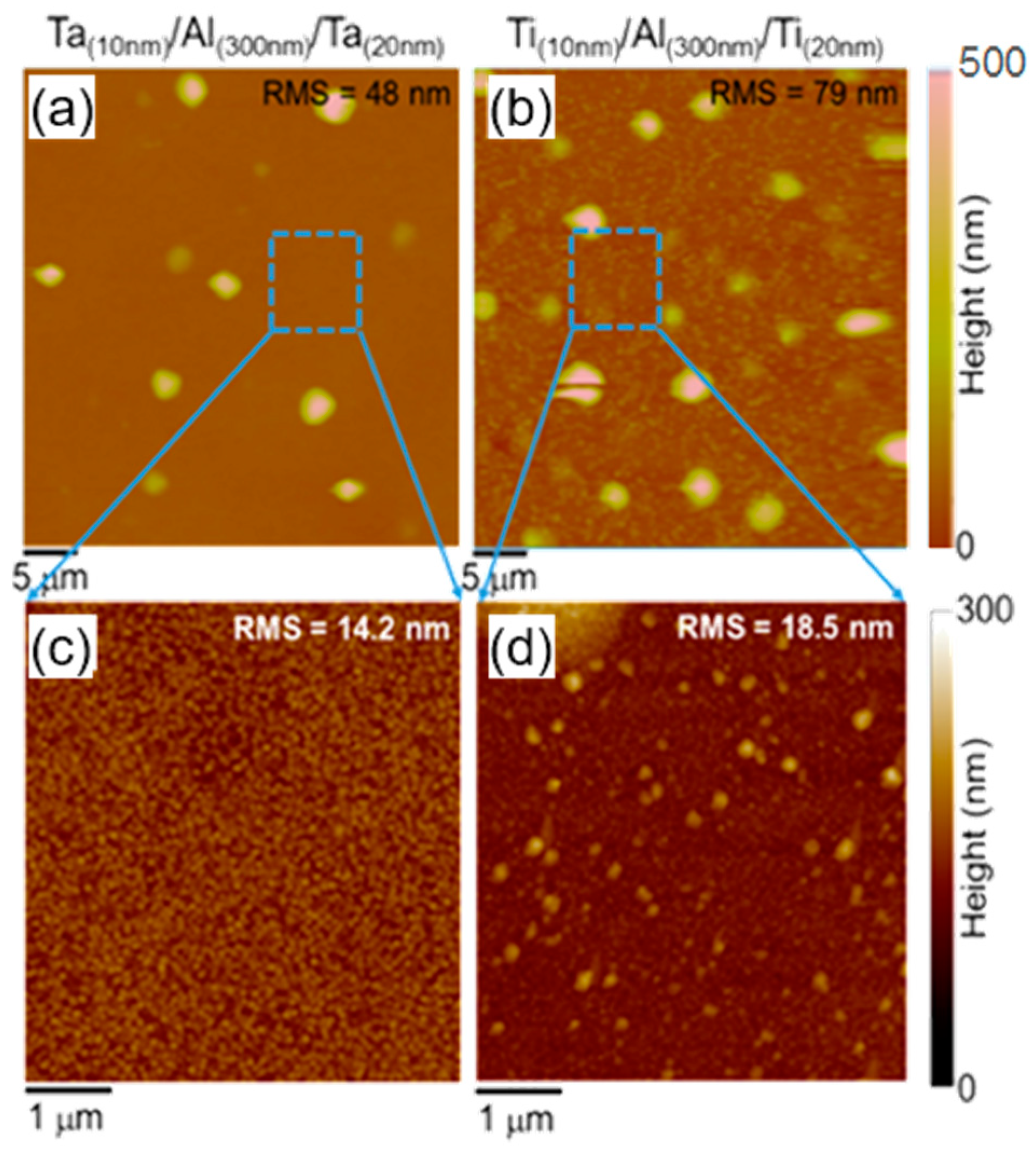
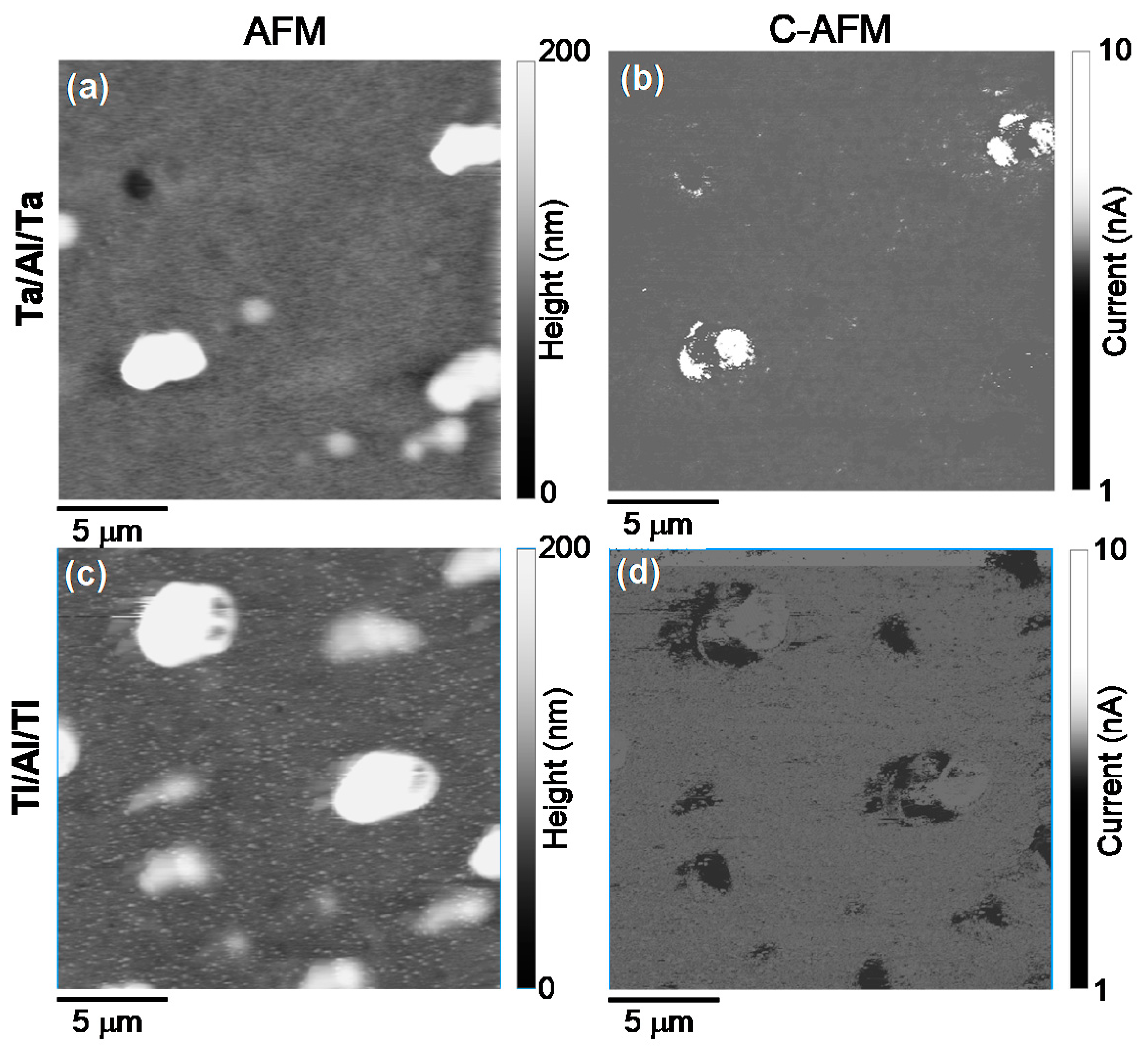
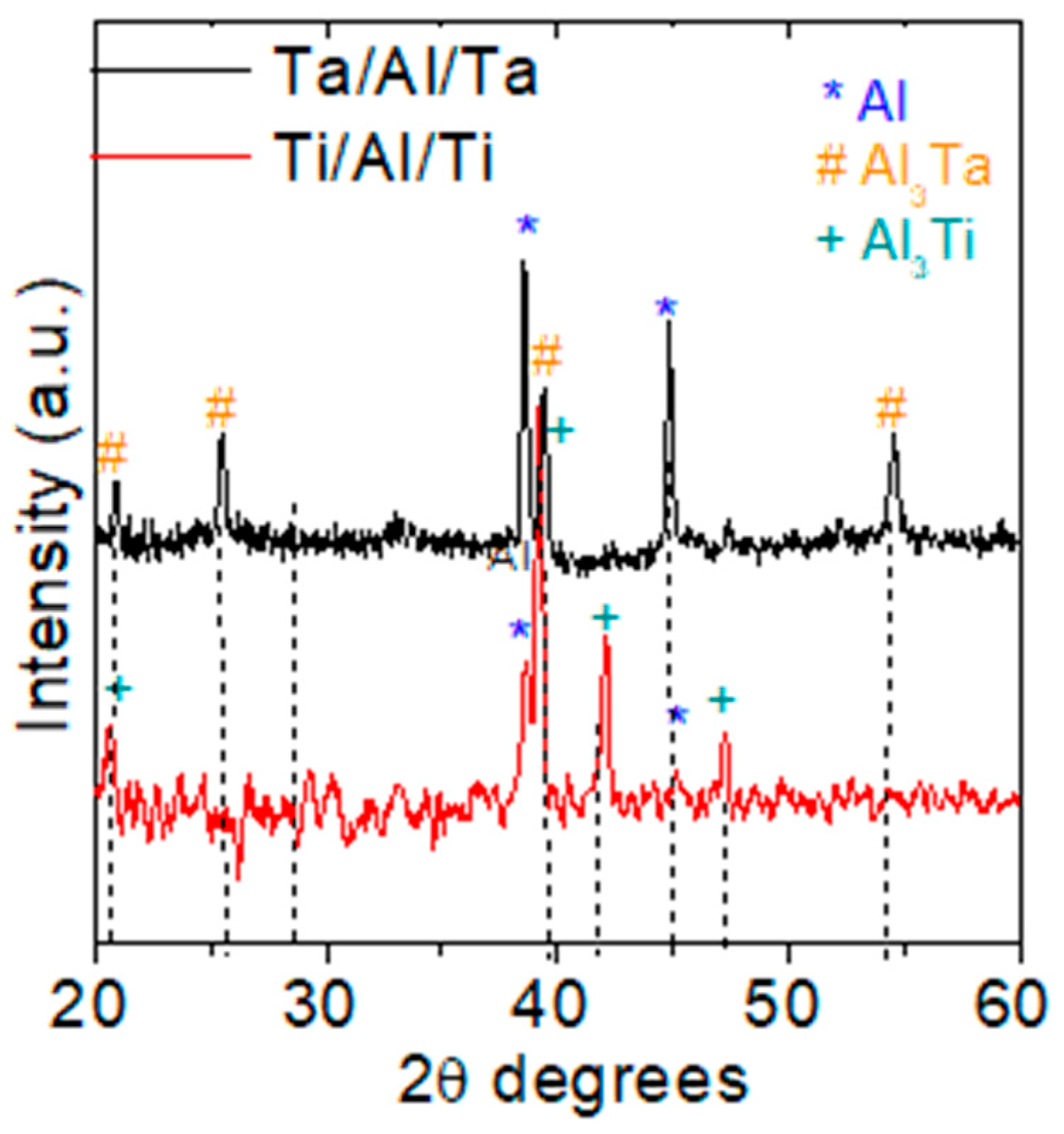
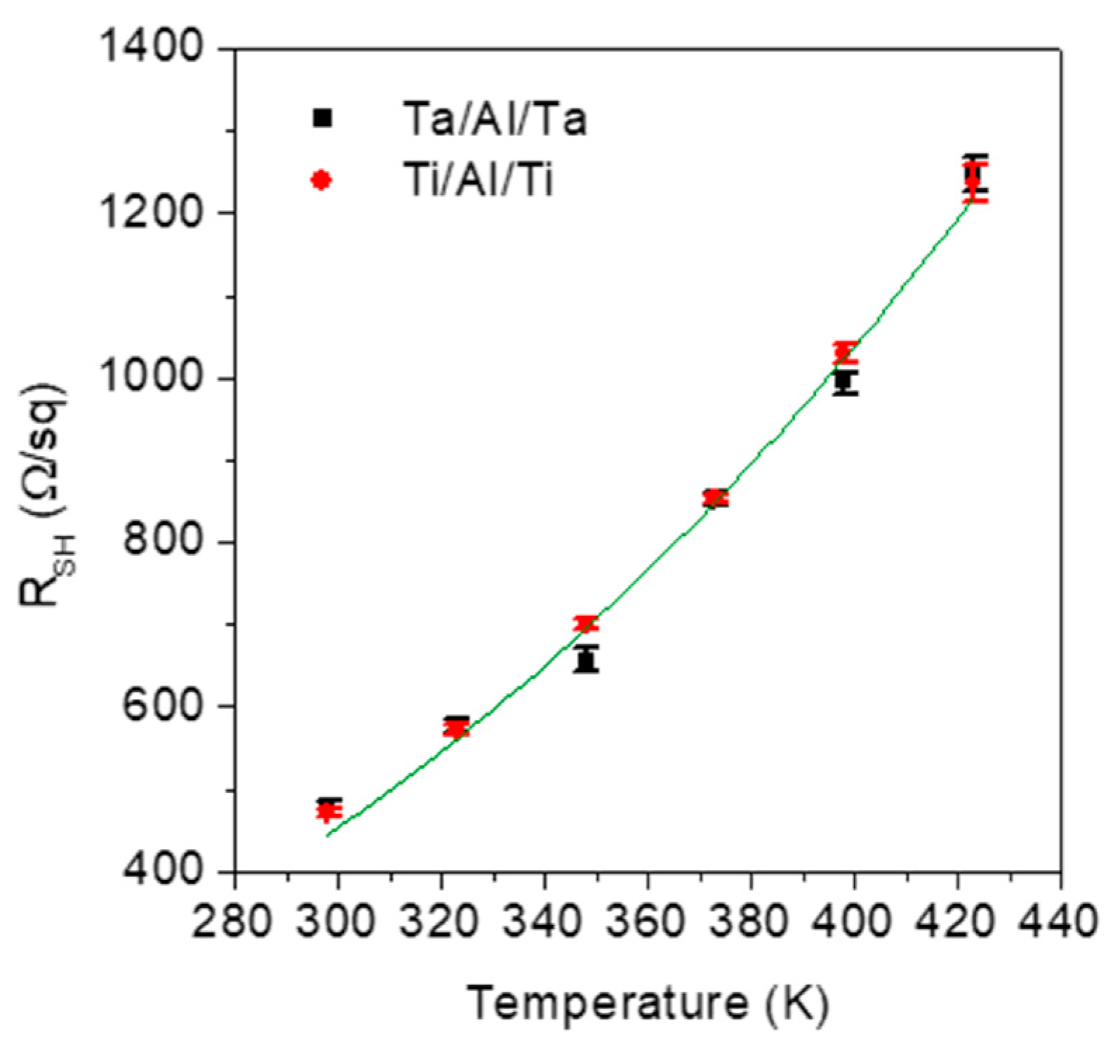
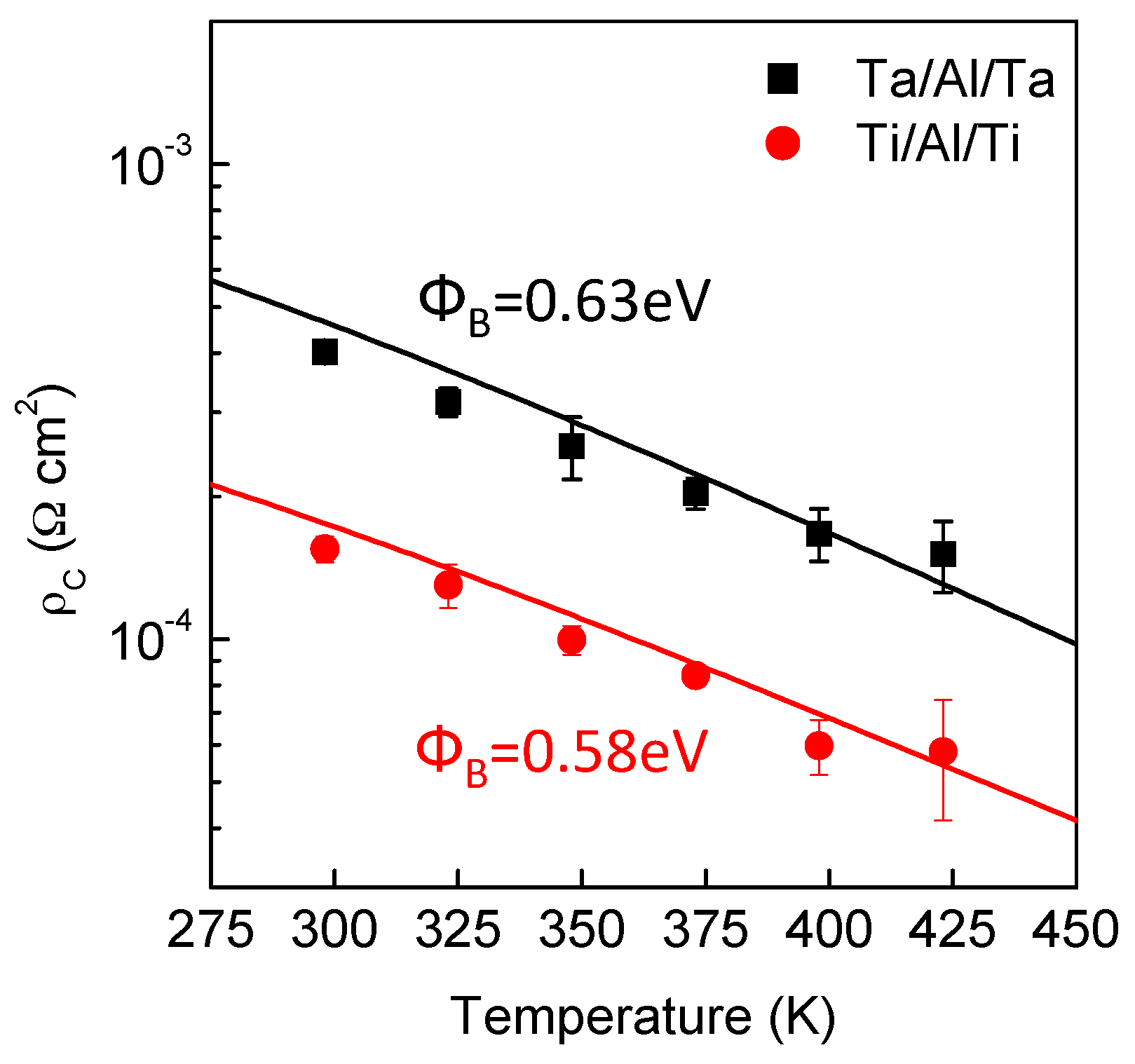
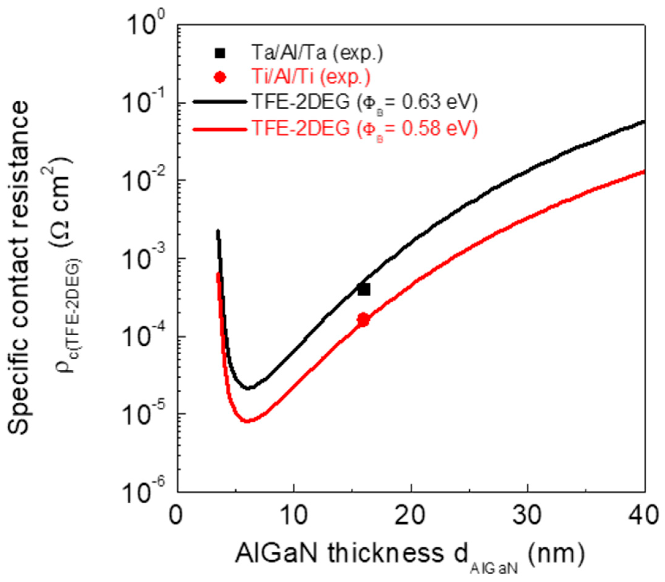
3. Results
4. Conclusions
Author Contributions
Funding
Acknowledgments
Conflicts of Interest
References
- Meneghini, M.; Meneghesso, G.; Zanoni, E. Power GaN Devices Materials, Applications and Reliability; Springer International Publishing: Basel, Switzerland, 2017. [Google Scholar]
- Roccaforte, F.; Fiorenza, P.; Greco, G.; Nigro, R.L.; Giannazzo, F.; Iucolano, F.; Saggio, M. Emerging trends in wide band gap semiconductors (SiC and GaN) technology for power devices. Microelectron. Eng. 2018, 187–188, 66–77. [Google Scholar] [CrossRef]
- Roccaforte, F.; Fiorenza, P.; Nigro, R.L.; Giannazzo, F.; Riv, G.G. Physics and technology of gallium nitride materials for power electronics. Nuovo Cimento 2018, 41, 625–681. [Google Scholar]
- Greco, G.; Iucolano, F.; Roccaforte, F. Ohmic contacts to Gallium Nitride materials. Appl. Surf. Sci. 2016, 383, 324. [Google Scholar] [CrossRef]
- Wang, L.; Mohammed, F.M.; Adesida, I. Differences in the reaction kinetics and contact formation mechanisms of annealed Ti∕Al∕Mo∕Au Ohmic contacts on n-GaN and AlGaN∕GaN epilayers. Appl. Phys. 2007, 101, 013702. [Google Scholar] [CrossRef]
- Iucolano, F.; Greco, G.; Roccaforte, F. Correlation between microstructure and temperature dependent electrical behavior of annealed Ti/Al/Ni/Au Ohmic contacts to AlGaN/GaN heterostructures. Appl. Phys. Lett. 2013, 103, 201604. [Google Scholar] [CrossRef]
- Mohammad, S.N. Contact mechanisms and design principles for alloyed ohmic contacts to n-GaN. J. Appl. Phys. 2004, 95, 7940. [Google Scholar] [CrossRef]
- Roccaforte, F.; Iucolano, F.; Giannazzo, F.; Alberti, A.; Raineri, V. Nanoscale carrier transport in Ti∕Al∕Ni∕Au Ohmic contacts on AlGaN epilayers grown on Si(111). Appl. Phys. Lett. 2006, 89, 022103. [Google Scholar] [CrossRef]
- Iucolano, F.; Roccaforte, F.; Alberti, A.; Bongiorno, C.; di Franco, S.; Raineri, V. Temperature dependence of the specific resistance in Ti∕Al∕Ni∕Au contacts on n-type GaN. J. Appl. Phys. 2006, 100, 123706. [Google Scholar] [CrossRef]
- Tripathy, S.; Lin, V.K.X.; Dolmanan, S.B.; Tan, J.P.Y.; Kajen, R.S.; Bera, L.K.; Teo, S.L.; Kumar, M.K.; Arulkuumanaran, S.; Ng, G.I.; et al. AlGaN/GaN two-dimensional-electron gas heterostructures on 200 mm diameter Si(111). Appl. Phys. Lett. 2012, 101, 082110. [Google Scholar] [CrossRef]
- Marcon, D.; de Jaeger, B.; Halder, S.; Vranckx, N.; Mannaert, G.; van Hove, M.; Decoutere, S. Manufacturing Challenges of GaN-on-Si HEMTs in a 200 mm CMOS Fab. IEEE Trans. Semicond. Manufact. 2013, 26, 361. [Google Scholar] [CrossRef]
- Liu, X.; Zhan, C.; Chan, K.W.; Liu, W.; Tan, L.S.; Chen, K.J.; Yeo, Y.C. AlGaN/GaN-on-Silicon Metal–Oxide–Semiconductor High-Electron-Mobility Transistor with Breakdown Voltage of 800 V and On-State Resistance of 3 mΩcm2 Using a Complementary Metal–Oxide–Semiconductor Compatible Gold-Free Process. Appl. Phys. Express 2012, 5, 066501. [Google Scholar] [CrossRef]
- Malmros, A.; Blanck, H.; Rorsman, N. Electrical properties, microstructure, and thermal stability of Ta-based ohmic contacts annealed at low temperature for GaN HEMTs. Semicond. Sci. Technol. 2011, 26, 075006. [Google Scholar] [CrossRef]
- Costant, A.; Baele, J.; Coppens, P.; Qin, W.; Ziad, H.; de Backer, E.; Moens, P.; Tack, M. Impact of Ti/Al atomic ratio on the formation mechanism of non-recessed Au-free Ohmic contacts on AlGaN/GaN heterostructures. J. Appl. Phys. 2016, 120, 104502. [Google Scholar] [CrossRef]
- Pooth, A.; Bergsten, J.; Rorsman, N.; Hirshy, H.; Perks, R.; Tasker, P.; Martin, T.; Webster, R.F.; Cherns, D.; Uren, M.J.; et al. Morphological and electrical comparison of Ti and Ta based ohmic contacts for AlGaN/GaN-on-SiC HFETs. Microelectron. Reliab. 2017, 68, 2–4. [Google Scholar] [CrossRef]
- Greco, G.; Giannazzo, G.; Iucolano, F.; Nigro, R.L.; Roccaforte, F. Nanoscale structural and electrical evolution of Ta-and Ti-based contacts on AlGaN/GaN heterostructures. J. Appl. Phys. 2013, 114, 083717. [Google Scholar] [CrossRef]
- Van Daele, B.; van Tendeloo, G.; Ruythooren, W.; Derluyn, J.; Leys, M.R.; Germain, M. The role of Al on Ohmic contact formation on n-type GaN and AlGaN∕GaN. Appl. Phys. Lett. 2005, 87, 061905. [Google Scholar] [CrossRef]
- Firrincielli, A.; de Jaeger, B.; You, S.; Wellekens, D.; van Hove, M.; Decoutere, S. Au-free low temperature ohmic contacts for AlGaN/GaN power devices on 200 mm Si substrates. Jpn. J. Appl. Phys. 2014, 53, 04EF01. [Google Scholar] [CrossRef] [Green Version]
- Greco, G.; Iucolano, F.; Bongiorno, C.; Giannazzo, F.; Krysko, M.; Leszczynski, M.; Roccaforte, F. Ti/Al ohmic contacts on AlGaN/GaN heterostructures with different defect density. Appl. Surf. Sci. 2014, 314, 546–551. [Google Scholar] [CrossRef]
- Greco, G.; Iucolano, F.; Bongiorno, C.; di Franco, S.; Nigro, R.L.; Giannazzo, F.; Prystawko, P.; Kruszewski, P.; Krysko, M.; Grzanka, E.; et al. Electrical and structural properties of Ti/Al-based contacts on AlGaN/GaN heterostructures with different quality. Phys. Status Solidi 2015, 212, 1091–1098. [Google Scholar] [CrossRef]
- E-Zammar, G.; Yvon, A.; Khalfaoui, W.; Nafouti, M.; Cayrel, F.; Collard, E.; Alquier, D. A simple non-recessed and Au-free high quality Ohmic contacts on AlGaN/GaN: The case of Ti/Al alloy. Mater. Sci. Semicond. Proc. 2018, 78, 107–110. [Google Scholar] [CrossRef]
- Berger, H.H. Models for contacts to planar devices. Solid State Electron. 1972, 15, 145–158. [Google Scholar] [CrossRef]
- Spera, M.; Miccoli, C.; Nigro, R.L.; Bongiorno, C.; Corso, D.; di Franco, S.; Iucolano, F.; Roccaforte, F.; Mater, G.G. Modification of the sheet resistance under Ti/Al/Ni/Au Ohmic contacts on AlGaN/GaN heterostructures. Sci. Semicond. Process. 2018, 78, 111. [Google Scholar] [CrossRef]
- Sujata, M.; Bhargava, S.; Sangal, S. On the formation of TiAl3 during reaction between solid Ti and liquid Al. J. Mater. Sci. Lett. 1997, 16, 1175. [Google Scholar] [CrossRef]
- Pretorius, R.; Vredenberg, A.M.; Saris, F.W.; de Reus, R. Silicide formation by concentration controlled phase selection. J. Appl. Phys. 1991, 70, 3636. [Google Scholar] [CrossRef]
- Hofman, T.; Kühne, P.; Schöche, S.; Chen, J.T.; Forsberg, U.; Janzén, E.; Sedrine, N.B.; Herzinger, C.M.; Woollam, J.A.; Schubert, M.; et al. Temperature dependent effective mass in AlGaN/GaN high electron mobility transistor structures. Appl. Phys. Lett. 2012, 101, 192102. [Google Scholar] [CrossRef] [Green Version]
- Liu, Z.H.; Arulkumaran, S.; Ng, G.I. Temperature dependence of Ohmic contact characteristics in AlGaN/GaN high electron mobility transistors from −50 to 200 °C. Appl. Phys. Lett. 2009, 94, 142105. [Google Scholar] [CrossRef]
- Gaska, R.; Yang, J.W.; Osinsky, A.; Chen, Q.; Khan, M.A.; Orlov, A.O.; Snider, G.L.; Shur, M.S. Electron mobility in modulation-doped AlGaN–GaN heterostructures. Appl. Phys. Lett. 1998, 72, 707. [Google Scholar] [CrossRef]
- Padovani, F.A.; Stratton, R. Field and thermionic-field emission in Schottky barriers. Solid-State Electron. 1966, 9, 695. [Google Scholar] [CrossRef]
- Takei, Y.; Kamiya, M.; Tsutsui, K.; Saito, W.; Kakushima, K.; Wakabayashi, H.; Kataoka, Y.; Iwai, H. Ohmic Contact Properties Depending on AlGaN Layer Thickness for AlGaN/GaN High Electron Mobility Transistor Structures. ECS Trans. 2014, 61, 265. [Google Scholar] [CrossRef]
- Yoshida, T.; Egawa, T. Dynamic variation of carrier transport properties of recessed Au-free ohmic contacts to InAlN/AlN/GaN on Si-wafer. Jpn. J. Appl. Phys. 2018, 57, 110302. [Google Scholar]
- Liu, Y.; Singh, S.P.; Kyaw, L.M.; Bera, M.K.; Ngoo, Y.J.; Tan, H.R.; Tripathy, S.; Lo, G.Q.; Chor, E.F. A Mechanisms of ohmic contact formation and carrier transport of low temperature annealed Hf/Al/Ta on In 0.18 Al 0.82 N/GaN-on-Si. ECS J. Solid. State Sci. Technol. 2015, 4, 30. [Google Scholar] [CrossRef]
- Nam, T.C.; Jang, J.S.; Seong, T.Y. Carrier transport mechanism of strained AlGaN/GaN Schottky contacts. Cur. Appl. Phys. 2012, 12, 1081. [Google Scholar] [CrossRef]
- Ambacher, O.; Smart, J.; Shealy, J.R.; Weimann, N.G.; Chu, K.; Murphy, M.; Schaff, W.J.; Eastman, L.F.; Dimitrov, R.; Wittmer, L.; et al. Two-dimensional electron gases induced by spontaneous and piezoelectric polarization charges in N- and Ga-face AlGaN/GaN heterostructures. J. Appl. Phys. 1999, 85, 3222. [Google Scholar] [CrossRef]
- Ibbetson, J.P.; Fini, P.T.; Ness, K.D.; DenBaars, S.P.; Speck, J.S.; Mishra, U.K. Polarization effects, surface states, and the source of electrons in AlGaN/GaN heterostructure field effect transistors. Appl. Phys. Lett. 2000, 77, 250. [Google Scholar] [CrossRef]
- Lin, Y.J.; Chen, Y.M.; Cheng, T.J.; Ker, Q. Schottky barrier height and nitrogen–vacancy-related defects in Ti alloyed Ohmic contacts to n-GaN. J. Appl. Phys. 2004, 95, 571. [Google Scholar] [CrossRef]
- Luther, B.P.; Mohney, S.E.; Jackson, T.N.; Khan, M.A.; Chen, Q.; Yang, J.W. Investigation of the mechanism for Ohmic contact formation in Al and Ti/Al contacts to n-type GaN. Appl. Phys. Lett. 1997, 70, 57. [Google Scholar] [CrossRef]
- Motayed, A.; Bathe, R.; Wood, M.C.; Diouf, O.S.; Vispute, R.D.; Mohammad, S.N. Electrical, thermal, and microstructural characteristics of Ti/Al/Ti/Au multilayer Ohmic contacts to n-type GaN. J. Appl. Phys. 2003, 93, 1087. [Google Scholar] [CrossRef]
- Hajlasz, M.; Donkers, J.J.T.M.; Sque, S.J.; Heil, S.B.S.; Gravesteijn, D.J.; Rietveld, F.J.R.; Schmitz, J. Sheet resistance under Ohmic contacts to AlGaN/GaN heterostructures. J. Schmitz Appl. Phys. Lett. 2014, 104, 242109. [Google Scholar] [CrossRef]
- Lu, C.; Chen, H.; Lv, X.; Xie, X.; Mohammad, S.N. Temperature and doping-dependent resistivity of Ti/Au/Pd/Au multilayer ohmic contact to n-GaN. J. Appl. Phys. 2002, 91, 9218. [Google Scholar] [CrossRef]
- Kim, H.; Ryou, K.J.; Dupuis, R.D.; Lee, S.-N.; Park, Y.; Jeon, J.-W.; Seong, T.-Y. Electrical characteristics of contacts to thin film N-polar n-type GaN. Appl. Phys. Lett. 2013, 102, 052107. [Google Scholar]


© 2019 by the authors. Licensee MDPI, Basel, Switzerland. This article is an open access article distributed under the terms and conditions of the Creative Commons Attribution (CC BY) license (http://creativecommons.org/licenses/by/4.0/).
Share and Cite
Spera, M.; Greco, G.; Lo Nigro, R.; Scalese, S.; Bongiorno, C.; Cannas, M.; Giannazzo, F.; Roccaforte, F. Metal/Semiconductor Barrier Properties of Non-Recessed Ti/Al/Ti and Ta/Al/Ta Ohmic Contacts on AlGaN/GaN Heterostructures. Energies 2019, 12, 2655. https://doi.org/10.3390/en12142655
Spera M, Greco G, Lo Nigro R, Scalese S, Bongiorno C, Cannas M, Giannazzo F, Roccaforte F. Metal/Semiconductor Barrier Properties of Non-Recessed Ti/Al/Ti and Ta/Al/Ta Ohmic Contacts on AlGaN/GaN Heterostructures. Energies. 2019; 12(14):2655. https://doi.org/10.3390/en12142655
Chicago/Turabian StyleSpera, Monia, Giuseppe Greco, Raffaella Lo Nigro, Silvia Scalese, Corrado Bongiorno, Marco Cannas, Filippo Giannazzo, and Fabrizio Roccaforte. 2019. "Metal/Semiconductor Barrier Properties of Non-Recessed Ti/Al/Ti and Ta/Al/Ta Ohmic Contacts on AlGaN/GaN Heterostructures" Energies 12, no. 14: 2655. https://doi.org/10.3390/en12142655