Article

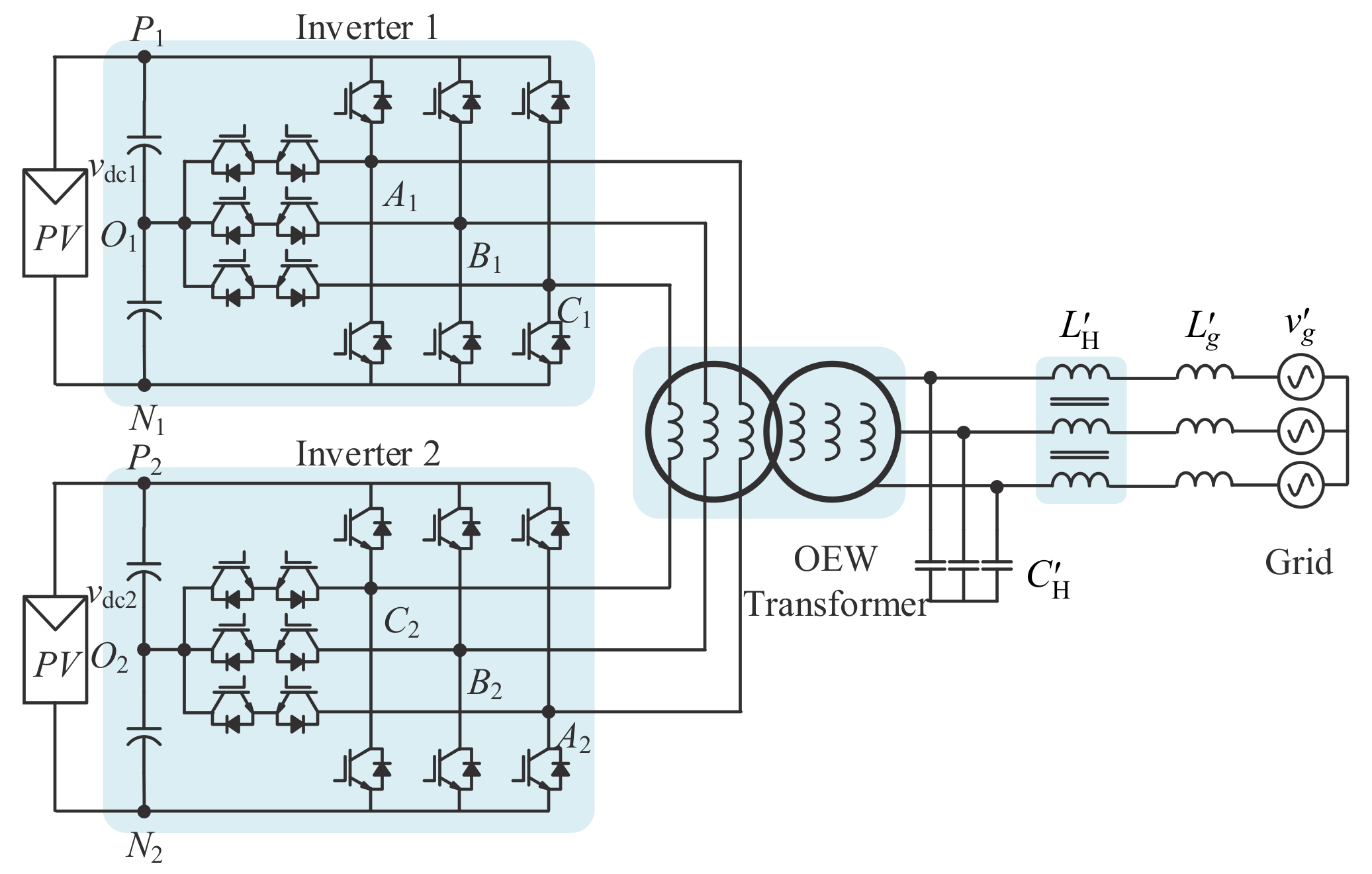
Research on the Filters for Dual-Inverter Fed Open-End Winding Transformer Topology in Photovoltaic Grid-Tied Applications

1
School of Electrical Engineering and Automation, Hefei University of Technology, Hefei 230009, China
2
Sungrow Power Supply Co., Ltd., Hefei 230088, China
*
Author to whom correspondence should be addressed.
Energies 2019, 12(12), 2338; https://doi.org/10.3390/en12122338
Submission received: 3 June 2019 / Revised: 14 June 2019 / Accepted: 17 June 2019 / Published: 18 June 2019

Abstract

:
Owing to the necessity of the transformer for the multi-parallel inverters connected to the medium-voltage (MV) grid, the conventional multi-parallel inverter topology can be reconfigured to the dual-inverter fed open-end winding transformer (DI-OEWT) topology to obtain lower output voltage harmonics, which can reduce the requirement of the filter inductance. However, due to the special structure of the DI-OEWT topology, the arrangement scheme of the filter can be more than one kind, and different schemes may affect the filter performance. In this paper, research on the existing two kinds of filters, as well as a proposed one, for the DI-OEWT topology used in photovoltaic grid-tied applications is presented. The equivalent circuits of these filters are derived, and based on this, the harmonic suppression capability of these filters is analyzed and compared. Furthermore, a brief parameter design method of these filters is also introduced, and based on the design examples, the inductance and capacitance requirements of these filters are compared. In addition, these filters are also evaluated in terms of the applicability for fault tolerance. At last, the analysis is verified through an experiment on a 30 kW dual-three-level inverter prototype.

1. Introduction

In recent years, the increasing exhaustion of traditional fossil energy has resulted in an emerging interest in the development of renewable energies, one of which is solar energy that has already obtained widespread applications. Among all types of commercial solar energy applications, photovoltaic grid-tied system plays an important role, and large-scale photovoltaic power plants have become dominant [1].
In the large-scale photovoltaic power plants, three-phase single-stage central inverters are widely used because of their many advantages, such as cost-effectiveness, simplicity in hardware design and easy maintenance. The two-level, three-level T-type, and three-level neutral point clamp (NPC) voltage source inverters (VSI) are the most widely used topologies among the current commercial central inverters [2]. Furthermore, to increase the transmission efficiency of the overall electrical equipment, the inverters are generally connected to a medium-voltage (MV) grid of a voltage level from 10 kV to 35 kV. Additionally, multi-parallel inverter topology, in which the inverters are connected in parallel through step-up MV transformers, are commonly used in these systems. A typical commercial application example is 1 MW MV turnkey station, which is composed of two 500 kW central inverters and one 1 MVA MV transformer [3]. Since the transformer is essential for the inverters connected to the MV grid, the multi-parallel inverter topology has the possibility to be reconfigured to the dual-inverter fed open-end winding transformer (denominated here as DI-OEWT) topology.
The dual-inverter topology was first proposed for the motor drive application in [4]. Since then, it has already been extended to many applications, such as STATCOM [5], active power filter [6], dynamic voltage restorer [7], photovoltaic grid-tied inverter [8]. It utilizes dual-inverter structure connected to the open-end windings of an induction motor or a three-phase transformer. Through proper modulation strategy, the harmonic cancellation effect can be realized among the two inverters, the dual-inverter topology with two N-level inverters can have the same output voltage levels as a (2N-1)-level inverter [9]. Therefore, lower dv/dt and lower harmonics in the output voltage can be obtained, which can reduce the filter requirement. It can also double the DC voltage utilization. A dual-N-level inverter with half the DC link voltage (compared to a conventional single inverter scheme) is capable of producing the same AC voltage as a single (2N-1) level inverter, which will reduce the voltage capacity of the power switch devices and decrease the switching losses [10]. What is more, the DC sources requirement of the dual-inverter is minimal over other multilevel topologies [11,12,13]. The two inverters of the dual-inverter can also be supplied by one single DC source for cost saving [14]. Another merit of the dual-inverter topology is the availability of higher redundant switching state combinations compared to the single inverter, which can be used to achieve switching frequency reduction [15], common-mode voltages suppression [16], capacitor voltage balance [17]. Furthermore, it also offers the advantage of fault tolerance. In case of a fault in the inverter, the inverter can still work with some adjustment [18,19,20].
However, the advantages of the dual-inverter topology described above are not all applicable to the topology used in photovoltaic grid-tied applications. Firstly, the DC bus voltage is limited to the photovoltaic array voltage, which is usually 1000 V or 1500 V (open-circuit voltage). It is uneconomic to reduce this voltage because that will increase the system installation costs and narrow the maximum power point tracking (MPPT) voltage operation range [2]. In addition, it will be better for the dual-inverter to be supplied by two separate arrays (two DC sources), which can not only achieve multiple MPPTs, but also suppress the circulating current among the two inverters [21,22]. The fault tolerance capability cannot be a special advantage of the dual-inverter because the multi-parallel inverter topology has the same capability as well. To sum up, compared with the conventional multi-parallel inverter topology, the most attractive advantage of the DI-OEWT topology is the improvement of the harmonic quality in the output voltages, thus can reduce the filter requirement and save the filter costs.
However, there are few papers considering the selection or design of the filters used in DI-OEWT-based grid-tied applications at present. In [23,24,25,26,27,28], single inductor filter was adopted in these DI-OEWT based grid-tied systems, which is obviously not a good choice. Owing to the weak harmonic suppression capability, it needs a large inductance value to meet the grid standard. To reduce the inductance cost, high order filter is preferred [29]. In [30], two kinds of high order filters for DI-OEWT topology were proposed. One is the “individual capacitor type filter”, that the two inverters of the DI-OEWT topology are connected to the open-end windings of the transformer through two individual inductor-capacitor filters. The other one is the “common capacitor type filter”, which is also presented in [21,22], that the two inverters are connected to the open-end windings of the transformer through two individual inductors but one common capacitor. However, the authors in [30] were mainly focused on active damping methods of the two different filters, and the authors in [21,22] were mainly focused on the magnetic integration design of the filter inductors, none of these papers analyzed the harmonic suppression capability or the parameter design method of these filters.
In addition, the transformer’s leakage inductance is a significant component of the filter, and for the transformer used in the high power MV grid-tied system, the value is usually no less than 6% [31]. This is a relatively big value and should be used properly in the selection and design of the filter, but none of the present literatures has paid attention to this. Another point deserves to be considered is the fault tolerance scheme of the DI-OEWT topology, which is very important for such multi-inverter type topology.
In light of the above, this paper aims to research the filters for the DI-OEWT topology used in photovoltaic grid-tied applications. First, the equivalent circuits of the existing two kinds of high order filters presented in [21,22,30] are derived, and based on this, the harmonic suppression capabilities of these filters are analyzed and compared. According to the analysis results, a new high order filter for DI-OEWT topology is also proposed. Furthermore, a brief parameter design method of the existing and the proposed filters for DI-OEWT is introduced and based on the design examples, the inductance and capacitance requirements of these filters are compared. Besides, these filters are also evaluated in terms of the applicability for fault tolerance.
The rest of the paper is organized as follows: The inductor-capacitor-inductor (LCL) filter used in multi-parallel inverters is presented in Section 2 as the comparison object. The model and harmonic suppression capability analysis of the existing and the proposed filters for DI-OEWT topology are shown in Section 3. The filter design method, together with the design examples, as well as the fault-tolerant scheme, are presented in Section 4. Experimental results are given in Section 5 to validate the filter parameters. Finally, the conclusions are summarized in Section 6.

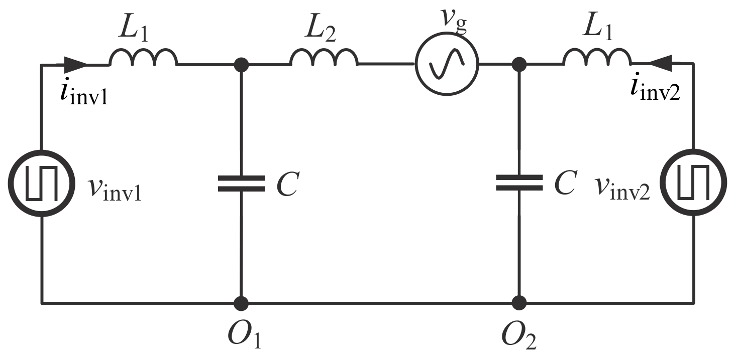
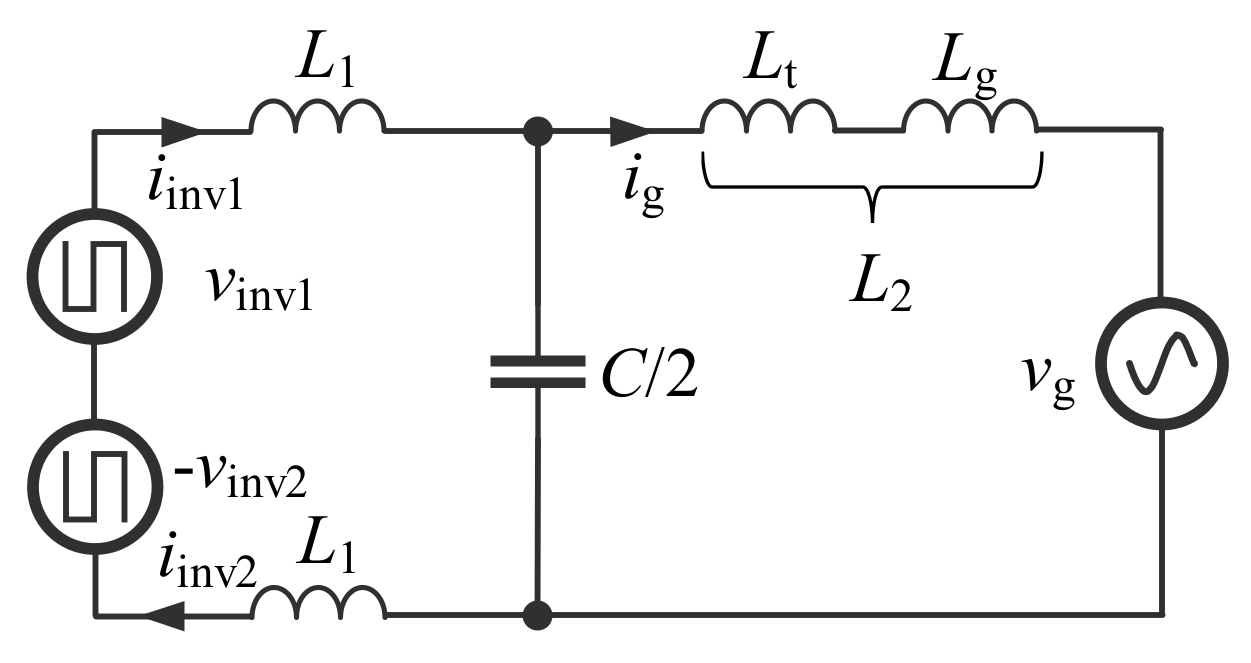
2. LCL Filter for the Conventional Multi-Parallel Inverters

The system configuration of the conventional multi-parallel inverters used in photovoltaic applications is illustrated in Figure 1. The two inverters are connected in parallel to the low voltage side of the MV transformer through individual LC filters. The leakage inductance L t of the transformer and the grid inductance L g play the role of the grid-side filter inductor, so the two inverters can also be viewed as connecting in parallel through individual LCL filters.
It is essential to derive the equivalent circuit of the filter based VSI for the filter design and harmonic suppression capability analysis. Since the LCL filter used in parallel inverters has no difference with that used in single inverters, the single-phase equivalent circuit of the LCL filter can be directly obtained from many existing papers [32,33], as shown in Figure 2. In the figure, the equivalent circuit is drawn referred to the low-voltage side of the transformer, vinv1 and iinv1 (take inverter 1 as an example) are the inverter output phase voltage and current, respectively. vg and ig are the grid voltage and current, respectively. The inverter-side inductor is represented as L1, the combined inductance of the transformer leakage inductance Lt and the grid inductance Lg are represented as L2, and the filter capacitor is represented as C.
While the inverter is working, the harmonics in iinv1 should be suppressed by the filter to limit the current ripple, and the harmonics in ig should be suppressed to meet the grid standard [34]. Assuming that no harmonics exist in the grid voltage, the inverter output voltage vinv1 is the only harmonic source of the system, then the transfer functions vinv1(s) to ig(s) and iinv1(s) can be used to reflect the harmonic suppression capability of the LCL filter, as shown in Equations (1) and (2), respectively
i g s = 1 L 1 L 2 C s 3 + L 1 + L 2 s v inv 1 s
i inv 1 s = L 2 C s 2 + 1 L 1 L 2 C s 3 + L 1 + L 2 s v inv 1 s
where L2 = Lt + Lg. The value of Lt and Lg is related to the transformer impedance voltage Vk and the grid short-circuit ratio (SCR), respectively [35]. Therefore, L2 can be calculated as
L 2 = 3 v g 2 2 π f 0 P rated V k + 3 v g 2 2 π f 0 P rated SCR = 3 v g 2 2 π f 0 P rated V k + 1 SCR
where Prated is the system rated power, f0 is the fundamental frequency.

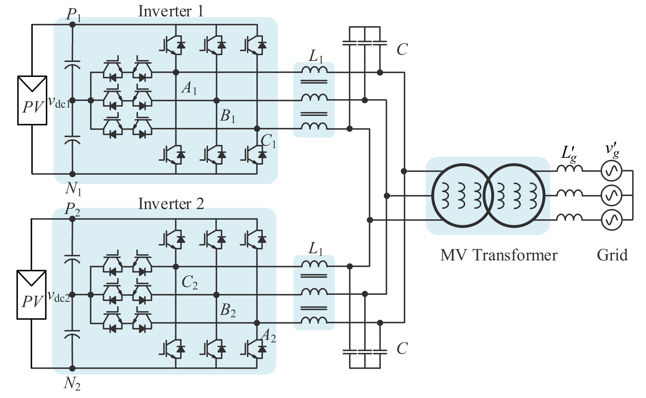
3. Existing and Proposed Filters for the DI-OEWT Topology

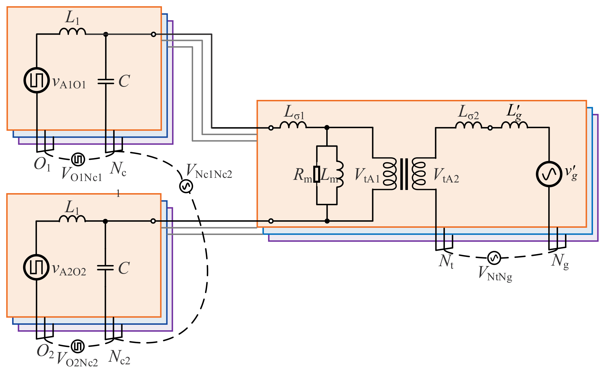
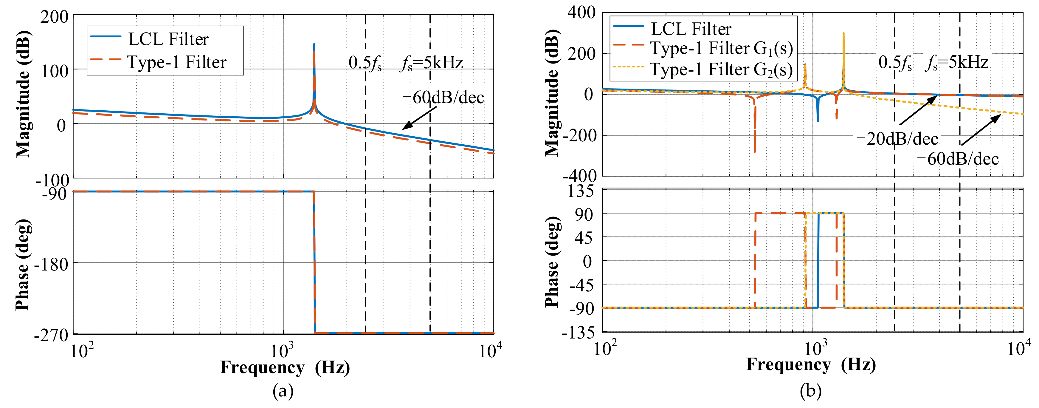
3.1. Type-1 Filter for the DI-OEWT Topology

Direct replacing of the two-winding transformer in the multi-parallel inverter topology (as shown in Figure 1) with the open-end winding (OEW) transformer, can obtain the DI-OEWT topology with the “individual capacitor type filter” (here we call it “Type-1 filter”). The filter was proposed in [30], as illustrated in Figure 3. It is worth noting that the voltage of the low-voltage side of the OEW transformer is twice the voltage of the replaced transformer, since the AC sides of the two inverters are connected in series through the low-voltage side of the transformer [8]. Accordingly, the current level of the inverter remains unchanged, so the multi-parallel inverter topology can be easily reconfigured to the DI-OEWT topology.
To analyze the Type-1 filter, firstly, the three-phase equivalent circuit of the DI-OEWT topology with the Type-1 filter is derived in Figure 4. The voltage source VX1O1 and VX2O2 represent the pole voltage of phase X1 of inverter 1 and the pole voltage of phase X2 of inverter 2, respectively (X = A, B, C). In a balanced and symmetrical three-phase system, for inverter 1, a common-mode (CM) voltage exists between the neutral point O1 and the capacitor common point Nc1, this CM voltage is expressed as VO1Nc1 = −1/3(VA1O1 + VB1O1 + VC1O1). Similarly, the corresponding CM voltage of inverter 2 is expressed as VO2Nc2 = −1/3(VA2O2 + VB2O2 + VC2O2). According to Kirchhoff’s voltage law (KVL), the voltage across the two capacitor common points Nc1, Nc2 can be derived as
V Nc 1 Nc 2 = 1 3 V CA 1 + V CB 1 + V CC 1 + V CA 2 + V CB 2 + V CC 2 + V L σ 1 A + V L σ 1 B + V L σ 1 C + V tA 1 + V tB 1 + V tC 1
The voltage across the neutral point Nt of the transformer high voltage side and the neutral point Ng of the three-phase grid can be derived as
V NtNg = 1 3 V tA 2 + V tB 2 + V tC 2 + V L σ 2 A + V L σ 2 B + V L σ 2 C + V LgA + V LgB + V LgC + v gA + v gB + v gC
In Equations (4) and (5), VCX1 and VCX2 represent the voltage on the filter capacitor of phase X1 and phase X2, respectively. VLσ1X and VLσ2X represent the phase X voltage on the leakage inductance at low voltage side (Lσ1) and high voltage side (Lσ2) of the MV transformer, respectively. VLgX represents the phase X voltage on the grid inductance L g . VtX1 and VtX2 represent the voltage of the low and high voltage side of the MV transformer, respectively. v gX is the phase X voltage of the MV grid. Considering only the line frequency component and the balanced three-phase system, it is easy to deduce that VNc1Nc2 = 0 and VNtNg = 0. Thus, Nc1 can be connected to Nc2 and Nt can be connected to Ng. Then, the single-phase equivalent circuit of the DI-OEWT topology with the Type-1 filter can be derived as shown in Figure 5 with further simplification. Where the inverter 1 output phase voltage vinv1 = VA1O1 + VO1Nc1, the inverter 2 output phase voltage vinv2 = VA2O2 + VO2Nc2, iinv1 and iinv2 represent the output phase current of inverter 1 and inverter 2, respectively.
From Figure 5, the transfer functions vinv1(s), vinv2(s) to ig(s) and iinv1(s) can be, respectively, calculated as
i g s = 1 L 1 L 2 C s 3 + 2 L 1 + L 2 s v inv 1 s v inv 2 s
i inv 1 s = G 1 s v inv 1 s G 2 s v inv 2 s
where
i inv 1 s = G 1 s v inv 1 s G 2 s v inv 2 s G 2 s = 1 L 1 2 L 2 C 2 s 5 + 2 L 1 2 C + 2 L 1 L 2 C s 3 + 2 L 1 + L 2 s
Figure 6a shows Bode plots of the transfer function vinv1(s), vinv2(s) to ig(s) of both the LCL filter and the Type-1 filter, while the inverter-side inductor L1, capacitor C, impedance voltage Vk and SCR are all the same in both filters. Figure 6b presents Bode plots of the transfer function vinv1(s), vinv2(s) to iinv(s) with the aforementioned parameters. According to Figure 6 and Equations (1), (2), (6), (7), the following can be obtained.
(1) Figure 6a suggests that, for ig, Type-1 filter has superior high-frequency harmonic suppression capabilities than the LCL filter. Meanwhile, compare Equation (6) with (1), the harmonic source of ig in DI-OEWT topology is vinv1vinv2, while in multi-parallel inverter topology is vinv1. Owing to the harmonic cancellation effect in the output voltage of DI-OEWT, vinv1vinv2 has lower harmonics than vinv1. Thus, ig in DI-OEWT can achieve a much better current quality than the multi-parallel inverter topology. Conversely, Type-1 filter can reduce filter requirement than LCL filter. Since L2 is limit by the Vk and SCR, which cannot be reduced, so L1 or C may be reduced.
(2) From Equation (7), for the inverter output phase current iinv1, G1(s) and G2(s) can reflect the suppression capability of the Type-1 filter on vinv1 and vinv2, respectively. From Figure 6b, in the high-frequency band, the harmonics attenuation rate of G2(s) is −60 dB/dec, way above the harmonics attenuation rate of G1(s), which is −20 dB/dec. Therefore, the harmonic source of iinv1 in DI-OEWT topology is mainly the vinv1, the same as the voltage in multi-parallel inverter topology according to Equation (2). Meanwhile, the harmonics attenuation rate of LCL filter is also −20 dB/dec, thus, iinv1 of both the scheme has almost the same current quality. Because the current ripple of iinv1, which is mainly suppressed by inverter-side inductor L1, is strictly limited by the semiconductor current rating and loss requirement. Therefore, L1 of Type-1 filter cannot be reduced.
In summary, compared with the multi-parallel inverter topology, the DI-OEWT topology with Type-1 filter can only reduce the value of filter capacitor C, showing that the Type-1 filter maybe not a better solution for the DI-OEWT topology.
Another way to explain why the Type-1 filter has the above characteristics can be shown as follows. Firstly, the reason why the DI-OEWT topology can achieve multilevel output and lower harmonics in output voltages is the harmonic cancellation effect between the two inverters. However, the two individual sets of shunt capacitors of the Type-1 filter break this cancellation loop. Some high-frequency harmonics, which should have been canceled, flow through these capacitors, leading to the increase of filter burden. In other words, Type-1 filter does not make judicious use of the merit of the DI-OEWT topology.

3.2. Type-2 Filter for the DI-OEWT Topology

The above analysis suggests that the special working characteristic (the harmonic cancellation characteristic) of the DI-OEWT topology should be considered when designing the filter. The “common capacitor type filter” (here we call it “Type-2 filter”) for DI-OEWT topology, which is presented in [21,22], seems to be a reasonable one, as illustrated in Figure 7. Two inverters are connected to a common shunt capacitor branch of the filter through the two inverter-side inductors, respectively. Then, the harmonic cancellation of the dual-inverter can be realized through the common capacitor branch. This common capacitor branch can be seen as the series connection of the two individual capacitor branches of the Type-1 filter, and the voltage rating of the former is the twice of the latter, so the actual value of the capacitor in Type-2 filter is half the value in Type-1 filter when the two has the same per unit (p.u.) value. Therefore, the capacitor here is represented as C/2.
Figure 8 shows the three-phase equivalent circuit of the DI-OEWT topology with the Type-2 filter. With the same derivation method as described in Section 3.1, we can get the corresponding single-phase equivalent circuit as illustrated in Figure 9. From the figure, the transfer functions vinv1(s), vinv2(s) to ig(s) and iinv1(s) can be, respectively, calculated as
i g s = 1 L 1 L 2 C s 3 + 2 L 1 + L 2 s v inv 1 s v inv 2 s
i inv 1 s = L 2 C / 2 s 2 + 1 L 1 L 2 C s 3 + 2 L 1 + L 2 s v inv 1 s v inv 2 s
It can be found from Equations (8) and (9) that the harmonic source of ig and iinv1 are all vinv1vinv2, proves once again that the Type-2 filter does make judicious use of the merit of the DI-OEWT topology.
Figure 10 shows the bode plots of the transfer functions vinv1(s), vinv2(s) to ig(s) and iinv1(s) of both the LCL filter and the Type-2 filter (with the same corresponding parameters), respectively. The figures suggest that, for both ig and iinv1, Type-2 filter has superior high-frequency harmonic suppression capabilities than the LCL filter. That can lead to a decreasing in the total inductance, capacitance, and volume. Therefore, the Type-2 filter can be an option for the DI-OEWT topology.
Furthermore, look again at Figure 9, it shows that the two inverter-side inductors L1 of the two inverters are actually connected in series, so these two inductors can merge into one single inductor, further reducing the volume and cost due to the saving of inductor magnetic cores. In this case, the complex magnetic integration method for reducing the inverter-side inductors’ magnetic component size, which was proposed in [22], is actually unnecessary.

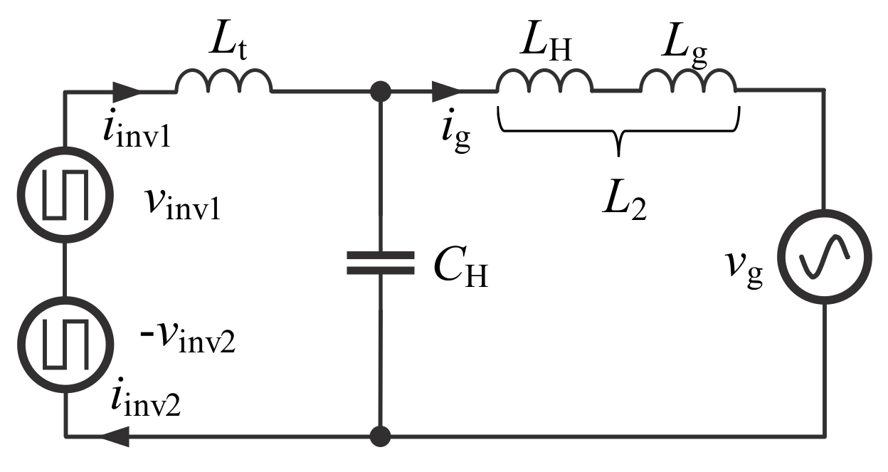
3.3. The Proposed Type-3 Filter for the DI-OEWT Topology

According to the above analysis of the existing filters for DI-OEWT topology, only Type-2 filter is suitable because its structure is fit for the working characteristic of the DI-OEWT topology. However, the leakage inductance of the transformer, which is a relatively large value in a high-power MV transformer, has not got special attention and rational utilization.
In Section 3.1, we have mentioned that the voltage of the low-voltage side of the OEW transformer is the twice of the replaced transformer. Then, it can be easy to deduce from Equation (3) that the leakage inductance of OEW transformer is four times as the replaced one (referred to the low-voltage side). Setting such a large inductance as the grid-side inductor may be not a cost-saving solution.
Therefore, in this paper, a new high order filter (here we call it “Type-3 filter”) for DI-OEWT topology is proposed, as illustrated in Figure 11. The two inverters are directly connected to the low-voltage side of the OEW transformer, the shunt capacitor C H and grid-side inductor L H are set at the high voltage side of the OEW transformer. In this filter, the harmonic cancellation effect of the DI-OEWT can be realized through the transformer, without any other shunt branch. The transformer leakage inductance Lt is used as the inverter-side inductor of the filter. If the initial value of Lt is not enough to suppress the inverter-side current ripple, it can be increased just by increasing the impedance voltage Vk of the transformer.
With the similar derivation method described above, here we directly give the single-phase equivalent circuit of the DI-OEWT topology with the Type-3 filter, as shown in Figure 12, where CH and LH represent the shunt capacitor and grid-side inductor referred to the low-voltage side, respectively.
From Figure 12, the transfer functions vinv1(s), vinv2(s) to ig(s) and iinv1(s) can be, respectively, calculated as
i g s = 1 L t L 2 C H s 3 + L t + L 2 s v inv 1 s v inv 2 s
i inv 1 s = L 2 C H s 2 + 1 L t L 2 C H s 3 + L t + L 2 s v inv 1 s v inv 2 s
As can be seen from comparing Figure 12 and Figure 9, the equivalent circuit of the Type-3 and Type-2 filter are actually the same, while the difference between them is the role of the leakage inductance of the OEW transformer. Due to this difference, the extra required capacitance and the inductance value of the two filters may be different. This different value should be compared with specific examples, which will be presented in the following section.

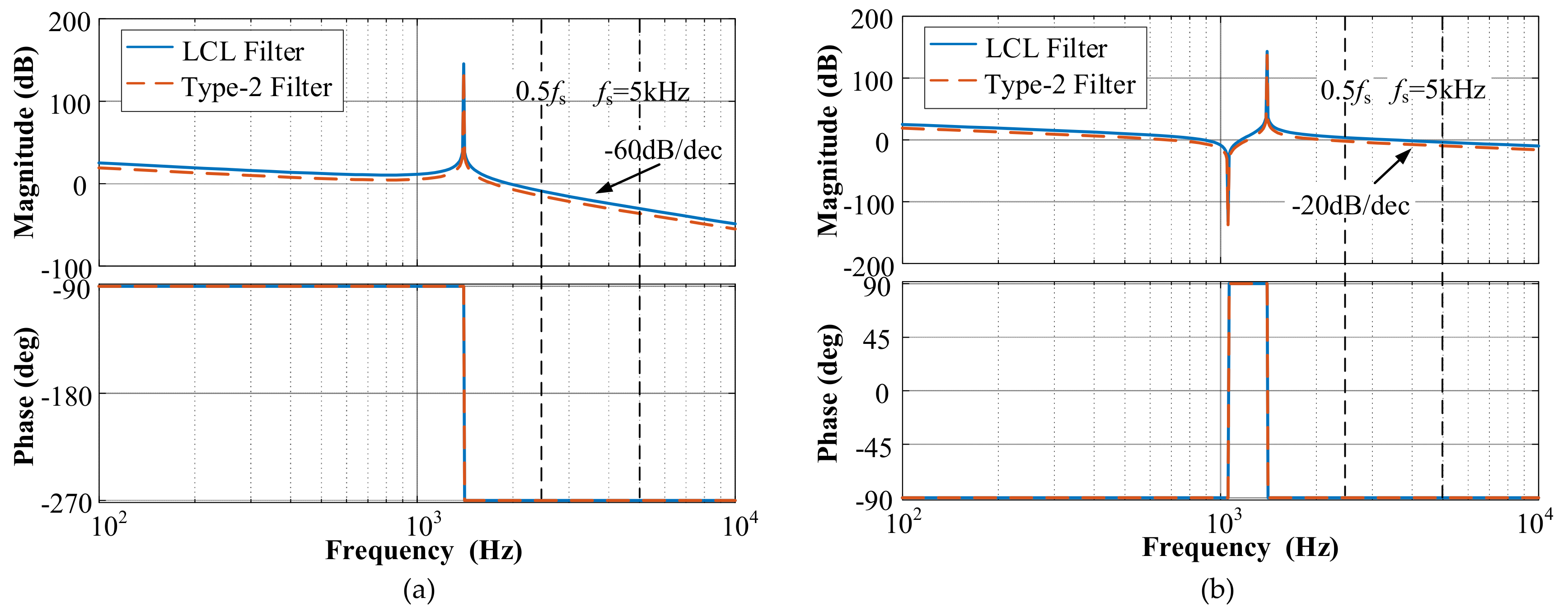
4. Parameter Design and Evaluations of the Filters

4.1. Parameter Design of the Filters

The design procedure of the Type-3 filter, together with the Type-1 and Type-2 filters, for the DI-OEWT topology is covered in the following. First, a 30 kW OEW dual-three-level (D3L) inverter, with 5 kHz switching frequency, 460 V~850 V (MPPT lower and upper limit voltage) DC voltage, 380 V line-to-line grid voltage is adopted. The primary side of the transformer is set as the OEW structure, and the secondary side of the transformer is connected in delta. It is worth noting that the primary side line-to-line voltage of the transformer in conventional multi-parallel inverter topology is usually 315 V, so the phase voltage ratio of the OEW transformer used here is 364 V/380 V, where 364 V = 2 × 315 V/1.732. In the following, the filter components calculations are presented on a per-unit basis, and the corresponding base values are listed in Table 1.
(1) Inverter-side Inductor: The inverter-side inductor value is determined by the requirement of the inverter-side current ripple, owing to the semiconductor current rating and efficiency requirement, this current ripple must be limited within a certain range. Besides, the equation for calculating the inductor value is related to the inverter topology as well as the modulation strategy, here the D3L inverter is modulated by the decoupled SVPWM strategy [17].
The decoupled SVPWM strategy has the characteristic that the total reference voltage signal is divided into two opposite parts for the two constituent inverters, and each of the inverter is switched independently of the other with the standard SVPWM strategy. Such characteristic is very appropriate for the two inverters tracking the individual MPPs. The space vector diagram of the individual three-level inverters is shown in Figure 13. In Figure 13, under the decoupled SVPWM strategy, the reference voltage space vector of the two inverters Vr1 and Vr2 are synthesized by the nearest three voltage vectors {V0, V1, V2} and { V 0 , V 3 , V 4 }, respectively. The pulse sequence is symmetrical with seven pieces of segments in each switching cycle Ts and the dwell times for each of the voltage vectors satisfy the following expression.
V 0 T 0 + V 1 T 1 + V 2 T 2 = V r 1 T s V 0 T 0 + V 3 T 3 + V 4 T 4 = V r 2 T s
The peak to peak value of the inductor current ripple is defined by volt-seconds applied to the inductor over the switching period [32,35]. For Type-1 filter, as mentioned in Section 3.1, the harmonic source of the inverter-side current is mainly the output phase voltage of one inverter. Take inverter 1 as an instance, the maximum current ripple occurs when the zero vector V0 dwell time T0 = 0, and the other two vectors V1 and V2 equally divide the switching period, T1 = T2 = Ts/2. In such case, the modulation index M = 1 / 3 and the DC voltage of the inverter is slightly larger than the MPPT upper limit voltage, the reference voltage vector Vr1 is in the midway between V1 and V2. The pulse sequence is degenerated into five pieces of segments and the corresponding inductor voltage and current waveform (take phase A1 as an example and vL1vinv1) are shown in Figure 14.
According to the volt-second balance principle, the following expression can be got as:
L 1 Δ i max = v dc 1 6 T s 4
where Δimax is the maximum current ripple.
From Equation (13), the minimum inverter-side inductor value of the Type-1 filter can be estimated by
L 1 min = v dc 1 24 Δ i max f s
where fs = 1/Ts is the switching frequency.
For Type-2 and Type-3 filter, the harmonic source of the inverter-side current is the difference between the output phase voltage of the two inverters (vinv1vinv2). The maximum current ripple will occur in the case that the reference voltage vector Vr1 is in the midway between V1 and V2, Vr2 is in the midway between V 3 and V 4 . In this case, T 0 = T 0 = 0 , T 1 = T 2 = T 3 = T 4 = T s / 2 . For the convenience of analysis, assuming vdc1 = vdc2 = vdc, then the inverter-side inductor voltage and current waveform of the Type-2 and Type-3 filter can be roughly derived as shown in Figure 15 (take phase A1-A2 as an example and vLvinv1vinv2).
Accordingly, the minimum inverter-side inductor value of the Type-2 and Type-3 filter can be derived based on the volt-second balance across the inductor as
L min = v dc 12 Δ i max f s
where L = 2L1 for Type-2 filter and L = Lt for Type-3 filter.
For the values vdc = 850 V, fs = 5000 Hz, and about 15% current ripple, the estimated minimum inverter-side inductor value for each filter can be calculated according to Equations (14) and (15) as follows:
Type-1 filter: two 0.02845 p.u. inductor;
Type-2 filter: one 0.0569 p.u. inductor;
Type-3 filter: transformer leakage inductance, 0.06 p.u..
(2) Grid-side Inductor and Shunt Capacitor: The grid-side inductor and shunt capacitor together constitute a shunt network to suppress the grid current harmonics, so as to satisfy the standard. For example, recent published Chinese standard NB/T 32004-2018 [34] requires the harmonics greater than 35th should be less than 0.3% of the 30% of the rated fundamental current. Besides, the capacitor value is limited to the maximum absorbed reactive power at rated load and typically less than 5%. Moreover, the resonant frequency ωres of the filter is often chosen as Equation (16) with the intention of not creating resonance problem in the lower and higher parts of the harmonic spectrum.
10 × 2 π f B ω res 0.5 × 2 π f s
where the value of ωres is 2 L 1 + L 2 / L 1 L 2 C for Type-1, Type-2 filter and L t + L 2 / L t L 2 C H for Type-3 filter.
For Type-1 and Type-2 filter, the grid-side inductor value is limited by the transformer leakage inductance, and its value is 0.06 p.u. (neglect the grid inductance). The capacitor values of these two filters are computed considering the attenuation of the filter. For instance, the maximum harmonic of the grid current greater than 35th usually occurs around the switching frequency. To limit the maximum current harmonic lower than 0.3%, the capacitor value of these two filters can be computed from Equations (6) or (8) considering the most dominant harmonic V(h) around the switching frequency in the inverter output voltage spectrum as
C 2 π f B h 2 L 1 + L 2 I B × 2 × 30 % × 0.3 % V h + 1 L 1 L 2 2 π f B h 3 I B × 2 × 30 % × 0.3 % V h
where h is the most dominant harmonic order. For D3L inverter with the decoupled SVPWM, if the DC voltage and the power (or the modulation index) of the two inverters are all the same, the harmonic around the switching frequency can be totally cancelled. But when the two inverters are tracking the individual MPPs, the DC voltage and the power (or the modulation index) of the two inverters may be different, this total cancellation cannot be realized. Assuming the worst case that no harmonic cancellation occurs around the switching frequency harmonics, the most dominant harmonic order h = mf − 2, the value of the (mf − 2) order harmonic can be got from simulation on a single three-level inverter as V(mf − 2) ≈ 0.055 p.u. (20.2 V), where mf is the modulation frequency index, and the value here is 100 (5000 Hz/50 Hz). Then from Equation (17) a minimum value of C can be calculated as 0.0175 p.u. Considering the constraints illustrated in Equation (16) and taking a certain margin, the final capacitor value of Type-1 and Type-2 filter is chosen as 0.0208 p.u.
For Type-3 filter, both the grid-side inductor and the shunt capacitor need to be designed. Usually, we choose a larger capacitor to reduce the requirement of the grid-side inductor for saving cost. Here the capacitor is starting with the value as 0.0416 p.u. With the same methodology as above, to ensure the grid current to satisfy the harmonic requirement, the grid-side inductor value can be computed from Equation (10) as
L 2 2 π f B h L t I B × 2 × 30 % × 0.3 % V h + 1 2 π f B h L t C 2 π f B h 2 1 I B × 2 × 30 % × 0.3 % V h
Also, considering the value of the most dominant harmonic order V(mf − 2) ≈ 0.055 p.u., a minimum value of L2 can be calculated as 0.0218 p.u.. Considering (16) and taking a certain margin, the final value of L2 is selected as 0.0237 p.u.

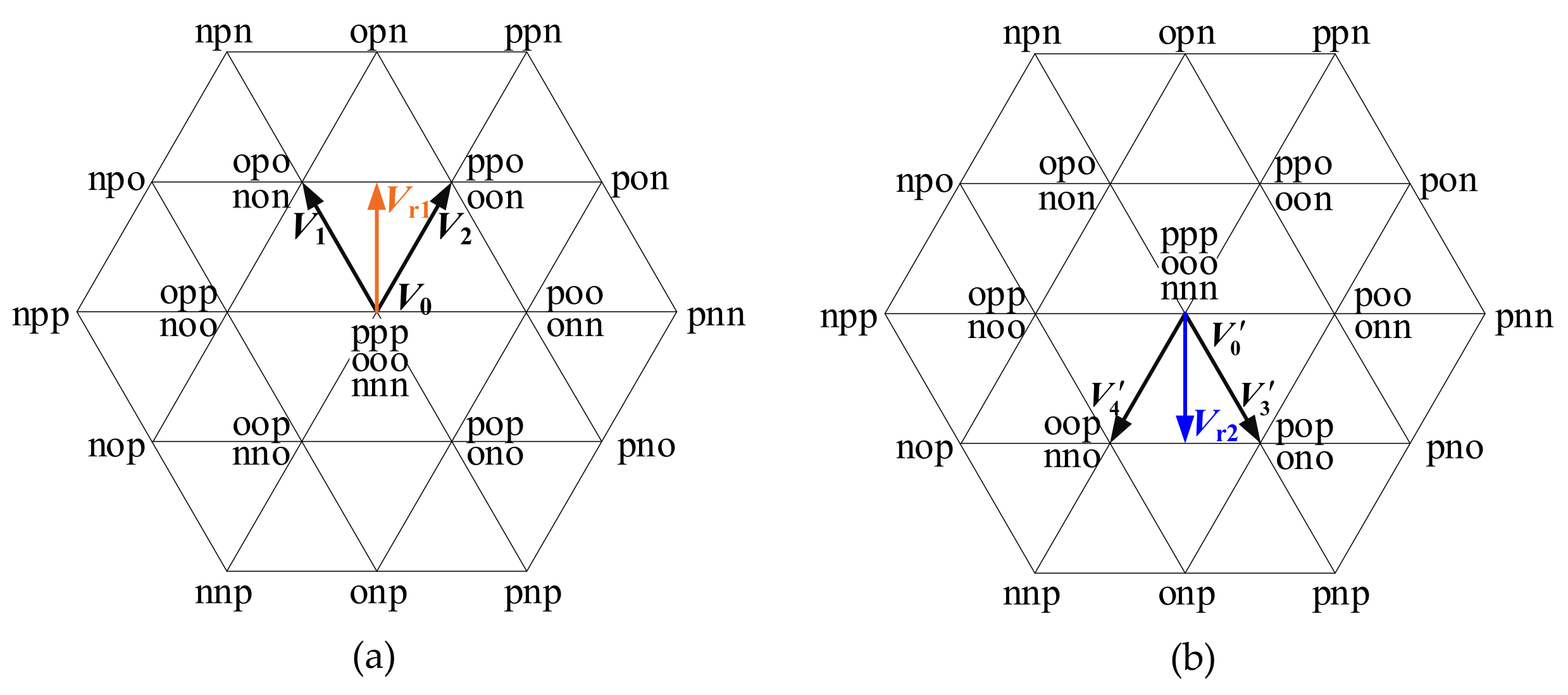
4.2. Fault-Tolerant Configuration for DI-OEWT Topology

Like the multi-parallel inverter topology, one of the advantages of the DI-OEWT topology is the availability of fault-tolerant operation. Many papers have investigated the fault-tolerant method for the dual-inverter topology used in motor drives, such as hybrid modulation strategies [18], dual-inverter topology reconfiguring method [19], fault-tolerant direct thrust force control method [20]. However, these methods are not suitable for the DI-OEWT topology used in photovoltaic applications, due to the DC voltages and power of the two inverters in such case are often different for the separate MPPT purpose.
To realize fault-tolerant operation in these systems, a more reasonable way is to cut off the fault inverter while allowing the healthy inverter to continue working. However, only one inverter cannot supply the whole voltage of the transformer due to the DC voltage limit, so the OEW transformer need to be reconfigured. Figure 16 presents a possible configuration to achieve the above purpose. As shown in the figure, a center-tapped (at the low voltage side) OEW transformer is used here, S1 and S2 are the contactors of the respective inverters connecting to the open-end windings of the transformer, S3 is the contactor to short the three-phase center-taps. In case of a fault in one inverter, the corresponding contactor (S1 or S2) of the fault inverter is switched off, and contactor S3 is switched on, then half of the primary windings are connected in star across the healthy inverter. The healthy inverter only needs to supply half of the original AC voltage, so that it can still work properly without any change.
Nevertheless, considering the configurations of the filters described above, not all types of filters are applicable for the presented fault-tolerant scheme. For DI-OEWT topology with the Type-1 and the proposed Type-3 filter, when a fault occurs in one inverter, the healthy inverter can still work through the modified filter. While for DI-OEWT topology with the Type-2 filter, fault-tolerant operation cannot be realized because the shunt capacitor cannot decouple from the faulty inverter.

4.3. Summary and Discussion

The designed parameters of the three kinds of filters, as well as the applicability of the presented fault-tolerant scheme on the filters, are summarized in Table 2.
From analyzing the table, the followings can be seen.
(1) The Type-1 and Type-2 filter have the same filter parameters, but the inverter-side inductor of the Type-1 filter needs two magnetic cores while the Type-2 filter only needs one, which means the Type-2 filter has a smaller size and cost than the Type-1 filter.
(2) Besides the transformer leakage inductance, the value of the extra inductance requirement of the Type-3 filter is reduced by a factor of 58.35%, while the capacitance requirement is increased about 50%, compared to the Type-1 and Type-2 filter.
(3) The total inductance of the Type-1 and Type-2 filter is more than 10% of the system base inductance, which may cause a larger fundamental voltage drop across the inductor and increase the DC voltage lower limit value.
(4) Unlike the Type-1 and Type-3 filter, the DI-OEWT topology with the Type-2 filter cannot realize fault-tolerant operations with the presented fault tolerate scheme.
(5) In terms of the inductance requirement, magnetic cores numbers and the fault-tolerant applicability, the proposed Type-3 filter has a certain advantage over the existing Type-1 and Type-2 filter.

5. Experiment Results

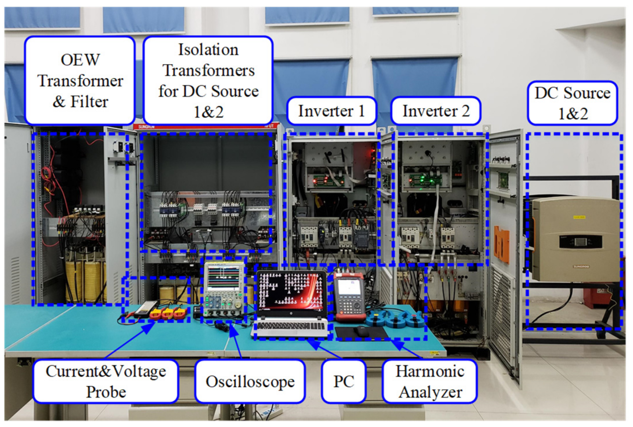
5.1. Experiment Setup Description

To verify the above analysis and design methodology, a 30 kW three-phase D3L inverter fed open-end winding transformer prototype based on DSP TMS320F28377D controller is constructed, as shown in Figure 17. The D3L inverter is supplied by two rectifiers (DC Source 1 and 2) with the DC voltage vdc = 850 V. The switching frequency of the inverter is 5 kHz. For the OEW transformer, the phase voltage ratio is 364 V/380 V, the leakage inductance is about 0.025 p.u., we compensate it to 0.06 p.u. through adding extra inductors.
The designed parameters of the three kinds of filters tabulated in Table 2 are tested by experiment. Here the D3L inverter with different filters are divided into three cases, where Case-1 represents the D3L inverter with the Type-1 filter, Case-2 represents the D3L inverter with the Type-2 filter, and Case-3 represents the D3L inverter with the Type-3 filter. In addition, the experimental analysis is carried out in two operating modes. One is the two inverters of the D3L inverter working at the power balance mode. Another one is the two inverters of the D3L inverter working at the power unbalance mode. Here, the power ratio of the two inverters is chosen as 3/2, corresponding to a relatively large imbalance ratio of 33.33%. Besides, to suppress the resonance caused by the high order filter, the filter based active damping method [36] is used here.

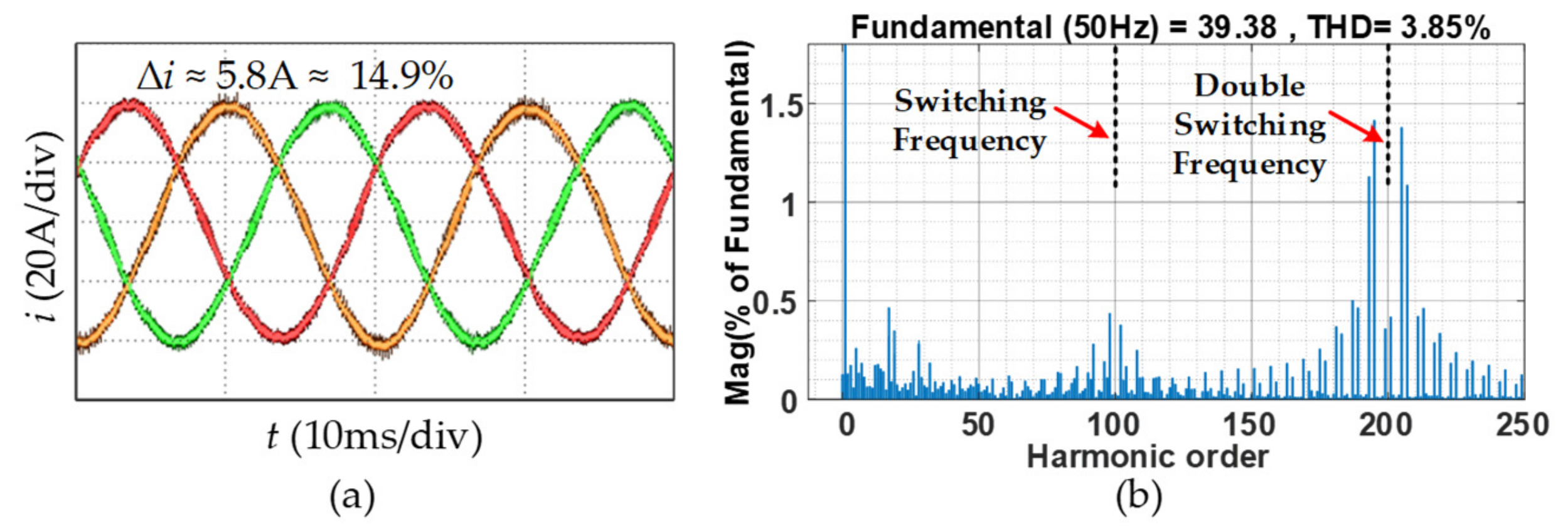
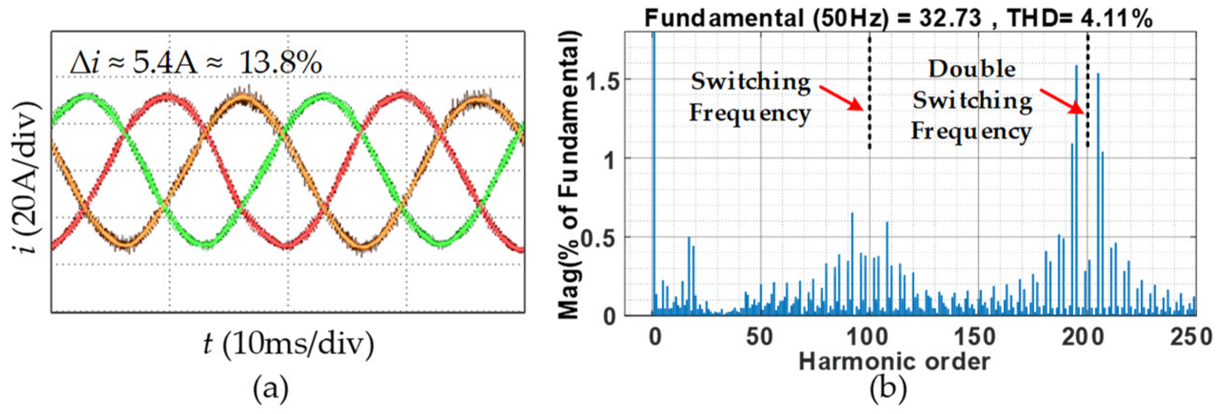
5.2. Inverter-Side Current Analysis

Figure 18, Figure 19 and Figure 20 show the experimental measured inverter-side currents and the corresponding fast Fourier transformation (FFT) waveforms of the three cases in power balance mode, respectively. From Figure 18a, Figure 19a, and Figure 20a, the inverter-side current ripple at the rated load in the three cases are around 14.9%, 14.6%, and 14.1%, respectively, which are roughly in agreement with the value calculated by Equations (14) and (15). From the FFT waveforms of the inverter-side currents as illustrated in Figure 18b, Figure 19b, and Figure 20b, it can be noticed that the current harmonics around the switching frequency are roughly canceled out in Case-2 and Case-3, but still exist in Case-1. The results demonstrate the analysis in Section 3 that the two individual sets of shunt capacitors of the Type-1 filter break the harmonic cancelation loop, causing the harmonics which should have been canceled still exist in the inverter-side current.
The experimental measured inverter-side currents and the corresponding FFT waveforms of the three cases in power unbalance mode are shown in Figure 21, Figure 22 and Figure 23, respectively. Observing these figures, when the D3L inverter is working in power unbalance mode, the inverter-side current ripple of the three cases are around 14.6%, 14.4%, and 13.8%, respectively, which are still within the design limit. Besides, as observed from Figure 22b and Figure 23b, the harmonics around the switching frequency also exist in the inverter-side currents in Case-2 and Case-3, which means that the total harmonic cancellation around the switching frequency cannot be realized in power unbalance mode.

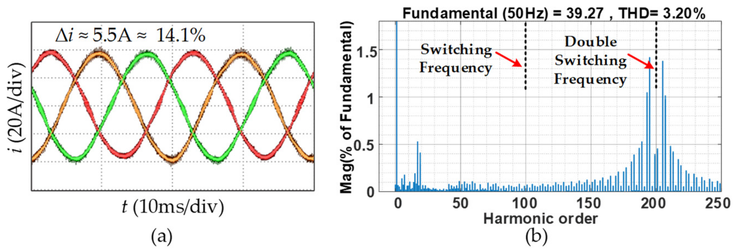
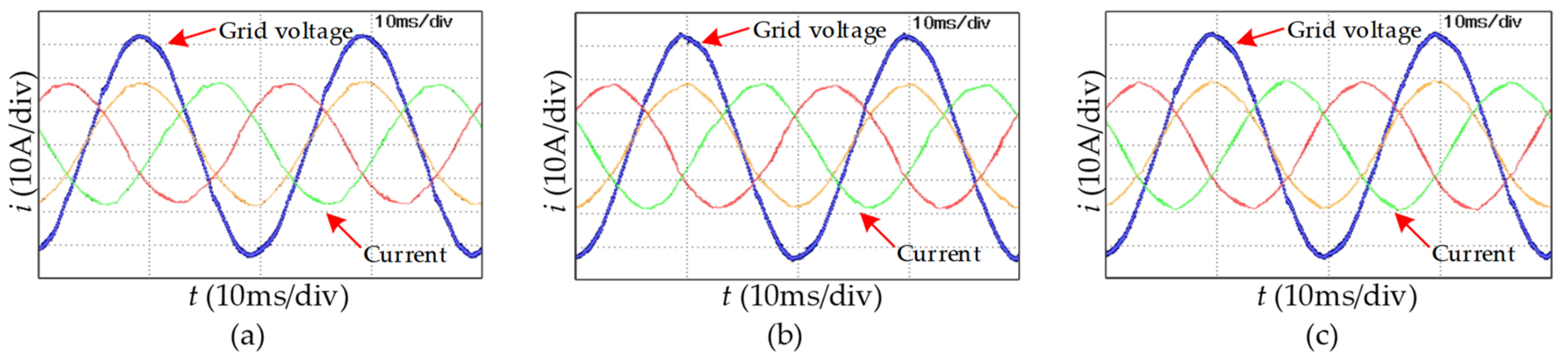
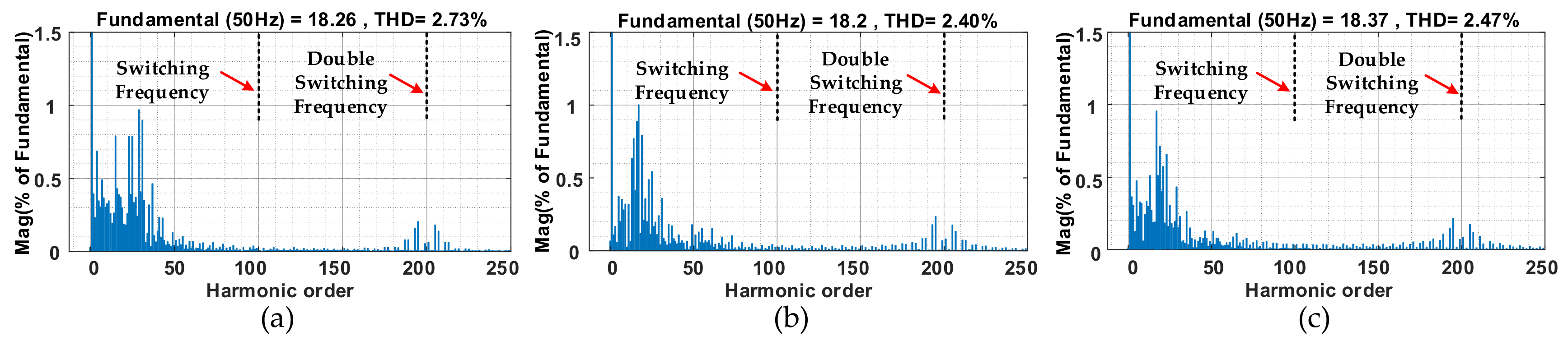
5.3. Grid Current Analysis

The experimental tests for the grid current are conducted at 30% load to verify whether the current quality satisfies the grid standard [34]. Figure 24 and Figure 25 show the grid current waveforms and the corresponding harmonic spectrums of the three cases in power balance mode, respectively. Figure 26 and Figure 27 show the grid current waveforms and the corresponding harmonic spectrums of the three cases in power unbalance mode, respectively. The test cases along with the grid current THD and the dominating current harmonic amplitude percentage (higher than 35th) are summarized in Table 3. As observed from the table, even though the inverter is working at 30% load, the current THD are all still below the 5% [34] limit, and the dominant harmonics (higher than 35th) are all within the 0.3% limit as well.
In summary, the analysis of the experimental inverter-side currents and the grid currents of all cases confirms the effectiveness of the filters’ parameters designed using the proposed method. Consequently, the discussions in Section 4.3 can be confirmed as well.

6. Conclusions

This paper investigates the filters for the DI-OEWT topology used in the photovoltaic grid-tied applications. The equivalent circuits of the existing Type-1 and Type-2 filter are derived in detail, and the corresponding harmonic suppression transfer functions are given. Some findings can be obtained from analyzing these equivalent circuits and the transfer functions, as well as comparing with the LCL filter used in the multi-parallel inverter topology. It can be found that Type-1 filter does not make judicious use of the merit (output harmonic cancellation) of the DI-OEWT topology, because its two individual sets of shunt capacitors break the cancellation loop. Another finding is that the two inverter-side inductors of the Type-2 filter are actually connected in series and can be merged into one single inductor to further reduce the filter volume and cost.
From the analysis of the existing filters and with consideration of the large leakage inductance value of the high power MV transformer, a new high order filter (named Type-3 filter) for DI-OEWT topology is also proposed. Unlike the existing filters, in which the transformer leakage inductance is set as the grid-side inductor, the Type-3 filter set the leakage inductance as the inverter-side inductor. Such an arrangement can maximize the transformer leakage inductance utilization, so as to reduce the requirement of the extra inductance.
A brief parameter design method for the three kinds of filters is also introduced. With the design examples of the three filters, the extra inductance requirement of the Type-3 filter can have a 58.35% higher reduction than the Type-1 and Type-2 filters. In addition, a fault tolerance scheme for DI-OEWT topology is also presented in the paper, but only Type-1 and Type-3 filters are applicable for the scheme. Finally, through evaluating the three filters in terms of the inductance requirement, magnetic core number and applicability for the fault tolerance scheme, the proposed Type-3 filter has a certain advantage over the existing Type-1 and Type-2 filters.
Experimental results of a 30 kW D3L inverter prototype verify the effectiveness of the proposed filter design method and validity of the analysis.
Besides the stability analysis, damping methods of the dual-inverter with the filters are also important issues, we will focus on these topics in future research.

Author Contributions

Conceptualization, B.W. and X.Z.; data curation, B.W.; formal analysis, B.W.; funding acquisition, X.Z. and R.C.; methodology, B.W.; experiment, B.W. and C.S.; writing—original draft, B.W.; writing—review & editing, B.W.

Funding

This work was funded by the National Natural Science Foundation of China (NO. U1766207).

Acknowledgments

The authors declare no acknowledgments.

Conflicts of Interest

The authors declare no conflict of interest.

Nomenclature

List of Abbreviations
LCLinductor-capacitor-inductor
MVmedium-voltage
DI-OEWTdual-inverter fed open-end winding transformer
NPCneutral point clamp
VSIvoltage source inverter
MPPTmaximum power point tracking
SCRshort-circuit ratio
OEWopen-end winding
CMcommon-mode
KVLKirchhoff’s voltage law
FFTfast Fourier transformation
p.u.per unit
List of Symbols
vinv1inverter 1 output phase voltage
vinv2inverter 2 output phase voltage
iinv1inverter 1 output phase current
iinv2inverter 2 output phase current
vggrid voltage
iggrid current
L1inverter-side inductor
Lttransformer leakage inductance
Lggrid inductance
L2combined inductance of Lt and Lg
Cfilter capacitor
C H shunt capacitor of Type-3 filter
L H grid-side inductor of Type-3 filter
CHshunt capacitor of Type-3 filter referred to the low-voltage side
LHgrid-side inductor of Type-3 filter referred to the low-voltage side
Vkimpedance voltage
Pratedsystem rated power
f0fundamental frequency
VX1O1pole voltage of phase X1 of inverter 1, X = A,B,C
VX2O2pole voltage of phase X2 of inverter 2
VO1Nc1CM voltage of inverter 1
VO2Nc2CM voltage of inverter 2
VNc1Nc2voltage across the two capacitor common points Nc1, Nc2
VNtNgvoltage across Nt and Ng
VCX1voltage on filter capacitor of phase X1
VCX2voltage on filter capacitor of phase X2
VLσ1Xphase X voltage on the leakage inductance at transformer low voltage side (Lσ1)
VLσ2Xphase X voltage on the leakage inductance at transformer high voltage side (Lσ2)
VLgXphase X voltage on the grid inductance
VtX1voltage of the low voltage side of the MV transformer
VtX2voltage of the high voltage side of the MV transformer
v gX phase X voltage of the MV grid
vdc1DC voltage of inverter 1
vdc2DC voltage of inverter 2
ωresfilter resonant frequency
Tsswitching period
fsswitching frequency
mfmodulation frequency index
hdominant harmonic order

References

  1. Zhao, Z.; Lei, Y.; He, F.; Lu, Z. Overview of large-scale grid-connected photovoltaic power plants. Autom. Electr. Power Syst. 2011, 12, 101–107. [Google Scholar]
  2. Serban, E.; Ordonez, M.; Pondiche, C. DC-bus voltage range extension in 1500 V photovoltaic inverters. IEEE J. Emerg. Sel. Top. Power Electron. 2015, 3, 901–917. [Google Scholar] [CrossRef]
  3. Sungrow. SG1250UD Inverter Product Datasheet. Available online: http://en.sungrowpower.com/product_view?id=146.html (accessed on 18 June 2019).
  4. Takahashi, I.; Ohmori, Y. High-performance direct torque control of an induction motor. IEEE Trans. Ind. Appl. 1989, 25, 257–264. [Google Scholar] [CrossRef]
  5. Anand, S.; Fernandes, B.G.; Chatterjee, K. DC voltage controller for asymmetric-twin-converter-topology-based high-power STATCOM. IEEE Trans. Ind. Electron. 2013, 60, 11–19. [Google Scholar] [CrossRef]
  6. De Almeida Carlos, G.A.; Jacobina, C.B.; dos Santos, E.C.; Fabrício, E.L.L.; dos Santos Rocha, N. Shunt active power filter with open-end winding transformer and series-connected converters. IEEE Trans. Ind. Appl. 2015, 51, 3273–3283. [Google Scholar] [CrossRef]
  7. De Almeida Carlos, G.A.; dos Santos, E.C.; Jacobina, C.B.; Mello, J.P.R.A. Dynamic voltage restorer based on three-phase inverters cascaded through an open-end winding transformer. IEEE Trans. Power Electron. 2016, 31, 188–199. [Google Scholar] [CrossRef]
  8. Grandi, G.; Rossi, C.; Ostojic, D.; Casadei, D. A new multilevel conversion structure for grid-connected PV applications. IEEE Trans. Ind. Electron. 2009, 56, 4416–4426. [Google Scholar] [CrossRef]
  9. Corzine, K.A.; Wielebski, M.W.; Peng, F.Z.; Wang, J. Control of cascaded multilevel inverters. IEEE Trans. Power Electron. 2004, 19, 732–738. [Google Scholar] [CrossRef]
  10. Edpuganti, A.; Rathore, A.K. New optimal pulsewidth modulation for single dc-link dual-inverter fed open-end stator winding induction motor drive. IEEE Trans. Power Electron. 2015, 30, 4386–4393. [Google Scholar] [CrossRef]
  11. Kubasiak, N.; Mercorelli, P.; Liu, S. Model predictive control of transistor pulse converter for feeding electromagnetic valve actuator with energy storage. In Proceedings of the 44th IEEE Conference on Decision and Control, Seville, Spain, 15 December 2005. [Google Scholar]
  12. Mercorelli, P. A multilevel inverter bridge control structure with energy storage using model predictive control for flat systems. J. Eng. 2013, 2013, 750190. [Google Scholar] [CrossRef]
  13. Mercorelli, P.; Kubasiak, N.; Liu, S. Multilevel bridge governor by using model predictive control in wavelet packets for tracking trajectories. In Proceedings of the IEEE International Conference on Robotics and Automation (ICRA), New Orleans, LA, USA, 26 April–1 May 2004; pp. 4079–4084. [Google Scholar]
  14. Kiadehi, A.D.; Drissi, K.E.K.; Pasquier, C. Adapted NSPWM for single DC-link dual-inverter fed open-end motor with negligible low-order harmonics and efficiency enhancement. IEEE Trans. Power Electron. 2016, 31, 8271–8281. [Google Scholar]
  15. Srinivas, S.; Ramachandra Sekhar, K. Theoretical and experimental analysis for current in a dual-inverter-fed open-end winding induction motor drive with reduced switching PWM. IEEE Trans. Ind. Electron. 2013, 60, 4318–4328. [Google Scholar] [CrossRef]
  16. Somasekhar, V.T.; Srinivas, S.; Kumar, K.K. Effect of zero-vector placement in a dual-inverter fed open-end winding induction motor drive with alternate sub-hexagonal center PWM switching scheme. IEEE Trans. Power. Electron. 2008, 23, 1584–1591. [Google Scholar] [CrossRef]
  17. Wu, D.; Wu, X.; Su, L.; Yuan, X.; Xu, J. A dual three-level inverter based open-end winding induction motor drive with averaged zero-sequence voltage elimination and neutral-point voltage balance. IEEE Trans. Ind. Electron. 2016, 63, 4783–4795. [Google Scholar] [CrossRef]
  18. Zhao, W.; Zhao, P.; Xu, D.; Chen, Z.; Zhu, J. Hybrid modulation fault-tolerant control of open-end windings linear vernier permanent-magnet motor with floating capacitor inverter. IEEE Trans. Power Electron. 2018, 34, 2563–2572. [Google Scholar] [CrossRef]
  19. Yu, Z.; Kong, W.; Jiang, D.; Qu, R.; Li, D.; Jia, S.; Sun, J.; Gan, C. Fault-tolerant control strategy of the open-winding inverter for DC-biased vernier reluctance machines. IEEE Trans. Power Electron. 2019, 34, 1658–1671. [Google Scholar] [CrossRef]
  20. Zhao, W.; Wu, B.; Chen, Q.; Zhu, J. Fault-tolerant direct thrust force control for a dual inverter fed open-end winding linear vernier permanent-magnet motor using improved SVPWM. IEEE Trans. Ind. Electron. 2018, 65, 7458–7467. [Google Scholar] [CrossRef]
  21. Gohil, G.; Bede, L.; Teodorescu, R.; Kerekes, T.; Blaabjerg, F. Dual-converter-fed open-end transformer topology with parallel converters and integrated magnetics. IEEE Trans. Ind. Electron. 2016, 63, 4929–4941. [Google Scholar] [CrossRef]
  22. Gohil, G.; Bede, L.; Teodorescu, R.; Kerekes, T.; Blaabjerg, F. Optimized integrated harmonic filter inductor for dual-converter-fed open-end transformer topology. IEEE Trans. Power Electron. 2017, 32, 1818–1831. [Google Scholar] [CrossRef]
  23. Kumar, N.; Saha, T.; Dey, J. Sliding-mode control of PWM dual inverter-based grid-connected PV system: Modeling and performance analysis. IEEE J. Emerg. Sel. Top. Power Electron. 2016, 4, 435–444. [Google Scholar] [CrossRef]
  24. Kumar, N.; Saha, T.K.; Dey, J. Control, implementation, and analysis of a dual two-level photovoltaic inverter based on modified proportional resonant controller. IET Renew. Power Gener. 2018, 12, 598–604. [Google Scholar] [CrossRef]
  25. Pires, V.F.; Foito, D.; Sousa, D.M. Conversion structure based on a dual T-type three-level inverter for grid connected photovoltaic applications. In Proceedings of the 2014 IEEE 5th International Symposium on Power Electronics for Distributed Generation Systems (PEDG), Galway, Ireland, 24–27 June 2014; pp. 1–7. [Google Scholar]
  26. Oleschuk, V.; Ermuratskii, V. Dual-inverter-based photovoltaic system with discontinuous synchronized PWM. In Proceedings of the 2014 IEEE International Conference on Intelligent Energy and Power Systems (IEPS), Kiev, Ukraine, 2–6 June 2014; pp. 86–89. [Google Scholar]
  27. Pires, V.F.; Martins, J.F.; Hao, C. Dual-inverter for grid connected photovoltaic system: modeling and sliding mode control. Sol. Energy 2012, 86, 2106–2115. [Google Scholar] [CrossRef]
  28. Anand, S.; Fernandes, B.G. Multilevel open-ended transformer based grid feeding inverter for solar photovoltaic application. In Proceedings of the IECON 2012-38th Annual Conference on IEEE Industrial Electronics Society, Montreal, QC, Canada, 25–28 October 2012; pp. 5738–5743. [Google Scholar]
  29. Beres, R.N.; Wang, X.; Blaabjerg, F.; Liserre, M.; Bak, C.L. Optimal design of high-order passive-damped filters for grid-connected applications. IEEE Trans. Power Electron. 2016, 31, 2083–2098. [Google Scholar] [CrossRef]
  30. Yin, J. Research on the Control Strategies of Dual Converter Based on Open-End Winding Topology. Ph.D. Dissertation, Beijing Jiaotong University, Beijing, China, April 2015; pp. 92–93. [Google Scholar]
  31. Siemens, A.G. GEAFOL Cast-Resin Transformer 100 to 16000 kVA. In Cast-Resin Transformers Catalog TV1; Siemens AG: München, Germany, 2007. [Google Scholar]
  32. Jiao, Y.; Lee, F.C. LCL filter design and inductor current ripple analysis for a three-level NPC grid interface converter. IEEE Trans. Power Electron. 2015, 30, 4659–4668. [Google Scholar] [CrossRef]
  33. Juntunen, R.; Korhonen, J.; Musikka, T.; Smirnova, L.; Pyrhönen, O.; Silventoinen, P. Comparative analysis of LCL-filter designs for paralleled inverters. In Proceedings of the 2015 IEEE Energy Conversion Congress and Exposition (ECCE), Montreal, QC, Canada, 20–24 September 2015; pp. 2664–2672. [Google Scholar]
  34. National Energy Administration. Technical Specification of PV Grid-Connected Inverter. NB/T 32004-2018; China. July 2018. Available online: https://www.chinesestandard.net/PDF/English.aspx/NBT32004-2018 (accessed on 18 June 2019).
  35. Rockhill, A.A.; Liserre, M.; Teodorescu, R.; Rodriguez, P. Grid-filter design for a multimegawatt medium-voltage voltage-source inverter. IEEE Trans. Ind. Electron. 2011, 58, 1205–1217. [Google Scholar] [CrossRef]
  36. Dannehl, J.; Liserre, M.; Fuchs, F.W. Filter-based active damping of voltage source converters with LCL filter. IEEE Trans. Ind. Electron. 2011, 58, 3623–3633. [Google Scholar] [CrossRef]
Figure 1. System configuration of the conventional multi-parallel inverters.
Energies 12 02338 g001
Figure 2. Single-phase equivalent circuit of the LCL filter.
Energies 12 02338 g002
Figure 3. System configuration of the dual-inverter fed open-end winding transformer (DI-OEWT) topology with the Type-1 filter.
Energies 12 02338 g003
Figure 4. Three-phase equivalent circuit of the DI-OEWT topology with the Type-1 filter.
Energies 12 02338 g004
Figure 5. Single-phase equivalent circuit of the DI-OEWT topology with the Type-1 filter.
Energies 12 02338 g005
Figure 6. Bode plots of transfer function vinv1(s), vinv2(s) to ig(s) and iinv1(s) in LCL and Type-1 filters (a) vinv1(s), vinv2(s) to ig(s), (b) vinv1(s), vinv2(s) to iinv1(s).
Energies 12 02338 g006
Figure 7. System configuration of the DI-OEWT topology with the Type-2 filter.
Energies 12 02338 g007
Figure 8. Three-phase equivalent circuit of the DI-OEWT topology with the Type-2 filter.
Energies 12 02338 g008
Figure 9. Single-phase equivalent circuit of the DI-OEWT topology with the Type-2 filter.
Energies 12 02338 g009
Figure 10. Bode plots of transfer functions vinv1(s), vinv2(s) to ig(s) and iinv1(s) in LCL filter and Type-2 filter. (a) vinv1(s), vinv2(s) to ig(s), (b) vinv1(s), vinv2(s) to iinv1(s).
Energies 12 02338 g010
Figure 11. System configuration of the DI-OEWT topology with the Type-3 filter.
Energies 12 02338 g011
Figure 12. Single-phase equivalent circuit of the DI-OEWT topology with the Type-3 filter.
Energies 12 02338 g012
Figure 13. Space vector diagram of the individual three-level inverters. (a) Inverter 1, (b) inverter 2.
Energies 12 02338 g013
Figure 14. Phase A1 inductor voltage and current waveform.
Energies 12 02338 g014
Figure 15. Phase A1-A2 inductor voltage and current waveform.
Energies 12 02338 g015
Figure 16. Fault-tolerant configuration of the DI-OEWT topology.
Energies 12 02338 g016
Figure 17. Experimental platform of the DI-OEWT grid-tied system.
Energies 12 02338 g017
Figure 18. Inverter-side current experimental waveforms of Case-1 in power balance mode. (a) Inverter-side current and current ripples. (b) FFT waveforms of the inverter-side current.
Energies 12 02338 g018
Figure 19. Inverter-side current experimental waveforms of Case-2 in power balance mode. (a) Inverter-side current and current ripples. (b) FFT waveforms of the inverter-side current.
Energies 12 02338 g019
Figure 20. Inverter-side current experimental waveforms of Case-3 in power balance mode. (a) Inverter-side current and current ripples. (b) FFT waveforms of the inverter-side current.
Energies 12 02338 g020
Figure 21. Inverter-side current experimental waveforms of Case-1 in power unbalance mode. (a) Inverter-side current and current ripples. (b) FFT waveforms of the inverter-side current.
Energies 12 02338 g021
Figure 22. Inverter-side current experimental waveforms of Case-2 in power unbalance mode. (a) Inverter-side current and current ripples. (b) FFT waveforms of the inverter-side current.
Energies 12 02338 g022
Figure 23. Inverter-side current experimental waveforms of Case-3 in power unbalance mode. (a) Inverter-side current and current ripples. (b) FFT waveforms of the inverter-side current.
Energies 12 02338 g023
Figure 24. Grid current experimental waveforms of the three cases in power balance mode. (a) Case-1. (b) Case-2. (c) Case-3.
Energies 12 02338 g024
Figure 25. Grid current FFT waveforms of the three cases in power balance mode. (a) Case-1, (b) Case-2, (c) Case-3.
Energies 12 02338 g025
Figure 26. Grid current experimental waveforms of the three cases in power unbalance mode. (a) Case-1, (b) Case-2, (c) Case-3.
Energies 12 02338 g026
Figure 27. Grid current FFT waveforms of the three cases in power unbalance mode. (a) Case-1, (b) Case-2, (c) Case-3.
Energies 12 02338 g027
Table 1. Per-unit base values of the system.
SymbolParameterFormulaValue
PBRated base power-30 kW
VBAc base voltage-364 V
IBAc base current P B / ( 3 V B ) 27.5 A
fBBase frequency-50 Hz
ZBBase impedance 3 V B 2 / P B 13.2496 Ω
LBBase inductance Z B / ( 2 π f B ) 42.17 mH
CBBase capacitance 1 / ( 2 π f B Z B ) 240 μF
Table 2. Comparison of the three kinds of filters.
FiltersType-1 FilterType-2 FilterType-3 Filter
Inverter-side Inductor0.02845 p.u. × 2
with 2 magnetic cores
0.0569 p.u.
with 1 magnetic core
Tr leakage inductance 0.06 p.u.
Grid-side InductorTr leakage inductance 0.06 p.u.Tr leakage inductance 0.06 p.u.0.0237 p.u.
Shunt CapacitoR0.0208 p.u.0.0208 p.u.0.0416 p.u.
Total Inductance0.1169 p.u.0.1169 p.u.0.0837 p.u.
Fault-tolerant applicabilityYesNoYes
Note: Tr represents the OEW transformer.
Table 3. THD and dominant harmonic percentage of grid current in different cases and modes.
CasesCase-1Case-2Case-3
Working ModesBalanceUnbalanceBalanceUnbalanceBalanceUnbalance
THD2.73%3.08%2.4%2.67%2.47%2.79%
Dominant Harmonic Percentage0.2%0.25%0.22%0.2%0.21%0.28%

