A Current-to-Voltage DC-DC Converter for Powering Backbone Devices of Scientific Cabled Seafloor Observatories


1
State Key Laboratory of Marine Geology, Tongji University, Shanghai 200092, China
2
School of Ocean and Earth Science, Tongji University, Shanghai 200092, China
3
Center for Marine Science and Technology, Tongji University, Shanghai 201306, China
*
Author to whom correspondence should be addressed.
Energies 2019, 12(12), 2261; https://doi.org/10.3390/en12122261
Submission received: 9 May 2019
/
Revised: 2 June 2019
/
Accepted: 10 June 2019
/
Published: 13 June 2019
Abstract
:In scientific cabled seafloor observatories, branching units and optical repeaters are essential backbone devices, in which zener diodes are commonly used in their power supply circuits. However, the low efficiency of zener-diode-based power feeding modules under large currents makes for a significant threat to the long-term reliability of backbone devices. In this paper, a novel full-bridge DC-DC converter with a duty-cycle-overlap control (DCOC) strategy is proposed to achieve high-efficiency current-to-voltage conversion. The circuit design of the converter and the principle of the DCOC strategy are analyzed. A prototype of the converter is implemented to demonstrate the feasibility of the proposed power feeding approach for large-scale cabled seafloor observatories.
1. Introduction
With the development of ocean science and technology, cabled seafloor observatories (CSOs) have become a powerful tool for oceanography research, realizing long-term and real-time observation of complex ocean processes [1,2]. CSOs can provide abundant power and high data bandwidth to support a number of in-situ scientific experiments in deep sea [3]. As illustrated in Figure 1, CSOs mainly consist of shore stations, primary nodes, junction boxes, instrument platforms, and single-conductor electro-optic submarine cables, as well as branching units (BUs) and optical repeaters as backbone devices [4,5]. Each BU connects backbone cables with a spur cable linking a primary node. In case a backbone or spur cable fault occurs, relevant power switches of the BU nearest to the fault must be opened to isolate the fault cable segment, so that the system can remain in normal operation. Moreover, the repeaters are used to compensate the loss of optical signals for the need of long-haul communication. Thus, these backbone devices are essential components of CSOs.
Generally, constant current (CC) and constant voltage (CV) direct current (DC) power systems are two types of CSOs [6], as illustrated in Figure 2. The CSOs powered by CV power sources can supply more power and have higher power transmission efficiencies than CC power-feeding CSOs, so that most scientific CSOs use CV power-feeding systems. As the backbone cables have only one conductor, the seawater is used as the current returning path.
In the traditional method, the power-supply modules of backbone devices are based on zener diodes. Connected in series with backbone cables, two back-to-back zener diodes can form a voltage regulation unit. A zener diode conducts when the DC voltage reaches its reverse breakdown voltage and then the reverse bias voltage remains stable. This method is compact in circuit configuration with high reliability, which is suitable for systems powered by low CC power sources around 0.65 A to 1.1 A. However, in large-scale CSOs with CV power-feeding systems, the backbone currents rise along with the increment in undersea payloads [7]. Thus, the efficiency of zener-diode-based (ZDB) modules decline rapidly, and large amount of power is dissipated in the form of heat, leading to over-temperature of electronic components in backbone devices. Hence, it is necessary to design a high-efficiency power-supply module for backbone devices of large-scale CSOs using CV power-feeding systems.
Similarly, in terrestrial DC power transmission systems, several methods have been proposed to tap power from the high-voltage DC line, i.e., the current-fed capacitor-switched converter [8], the current-fed inductor-switched converter [9], and the H-bridge DC-DC converter [10]. A new current-to-current converter is proposed for CC power-feeding CSOs [11]. In addition, various current-fed step-up conversion topologies have been proposed for some specific applications such as electric vehicles, servo-drive systems, uninterruptible power supplies (UPS) and photovoltaic systems, where low DC input voltages must be converted into higher DC output voltages. There are three basic current-fed topologies, which are push-pull [12], full-bridge [13], and half-bridge [14]. However, these current-fed converters need constant DC voltage inputs with unidirectional current, while the backbone cable voltages of CSOs vary with payloads and the cables only have one conductor with bidirectional current.
In this paper, we proposed a novel current-to-voltage full-bridge DC-DC converter based on high-frequency pulse-width-modulation (PWM) power switching technology for backbone devices of large-scale CSOs, with high power conversion efficiency and low heat dissipation. An earlier version of this paper was presented at the International Conference on OCEANS 2018.
2. Startup Operation of the Proposed Current-to-Voltage Converter
The purpose of the current-to-voltage converter design is to supply power for inner functional loads of backbone devices. As the converter needs to start up before its normal operation, a compact startup circuit is designed as shown in Figure 3.
The switch SA is normally-closed which is series connected with two back-to-back zener diodes. When the power feeding equipment (PFE) in the shore station comes into operation, the DC line current flows through SA and a steady voltage drop is generated across the diodes which can be used by the DC-DC isolation module to supply power for the inner circuits of the current-to-voltage converter. Once the converter starts up, the switching control circuit will turn off SA and isolate zener diodes from DC line.
3. Circuit Topology
The circuit topology of the proposed current-to-voltage converter is illustrated in Figure 4. Unlike conventional full-bridge DC-DC converters, there are eight solid-state switches in the power conversion circuit, of which four switches (Sa~Sd) are connected in reversal with the remains (S1~S4), respectively. The purpose of this design is to guarantee the normal operation of the proposed converter under bidirectional current.
It’s worth mentioning that the DC line current of CSOs is variable both in direction and value. In a CC power-feeding system, the current is always constant in normal operation. However, in case of a shunt fault to seawater, shore stations will reverse the polarity to prevent the corrosion of exposed conductor [15]. Similarly, the DC line current of a CV power-feeding system will also alter its direction and amplitude along with the operating modes [16]. Therefore, it is necessary for the converter to operate under the DC line bidirectional current.
The capacitor C1 is a key component in the process of power conversion. If the DC line current flows from up to down in Figure 4, the switches (Sa~Sd) will be passed by with some voltage drop across the diodes. Then the switches S1 to S4 operate at high frequency to alter the direction of the current flowing into C1 and the coupled transformer T1. At the beginning of a switching period, switches S1 and S4 are closed while S2 and S3 are open. The current flows into and charges C1. During the charging process, the voltage across C1 increases, so does the primary winding of T1. When the voltage reaches a preset value, S2 and S3 are switched on while S1 and S4 are switched off. The current flowing in C1 reverses its direction and then charges it in an opposite direction. Alternate repetition of this process will cause the generation of an alternating voltage across C1, and then the voltage can be transferred to the secondary side of T1, which then realizes the electrical isolation from the DC line.
4. Analysis of the Operating Principle
4.1. Steady-State Analysis
To analyze the steady state of the current-to-voltage converter, the equivalent model of the proposed converter is built, as shown in Figure 5. It is assumed that the switching frequency of switches and the capacitance of C1 have been determined, the turn ratio N2/N1 of the transformer T1 is 1:1, and the initial voltage across C1 is zero.
4.1.1. No-Load Condition
Figure 5a shows the equivalent power conversion circuit under the no-load condition. When the proposed converter operates, the current flows into C1 and T1, and then charges C1. Thus, the voltage across C1 increases gradually. After the voltage across C1 reaches the maximum value, C1 starts to discharge and releases the stored energy. The following time-domain equations can be derived in this process:
where C is the capacitance of C1, L is the inductance of the primary winding of T1, UC is the voltage across C1, UT is the voltage across the primary winding, IM is the DC current, IC is the charging current of C1, and IT is the current flowing into the primary winding. Solving the simultaneous equations, we can get the following results:
where t is smaller than . If t exceeds , IT will be equal to IM, while IC and UC will be zero. In that case, the power conversion circuit reaches a steady state until IM alters its direction.
4.1.2. Loading Condition
Figure 5b illustrates the equivalent power conversion circuit of the converter under the loading condition. In this process, the following equations can be built:
where R is the load resistance, UR is the load voltage, and IR is the load current. To solve the simultaneous equations, the results are as follows:
The values of s1, s2, k1 and k2 can be expressed as:
The above time-domain models suggest that the voltage UC is always generated across C1 under both no-load and loading conditions. When the input current flows into C1 and T1, it charges C1 and the capacitor voltage increases gradually until reaching the limited value. After the stored energy on C1 is released, the power conversion circuit reaches a steady state. Due to the switching operation, the current which flows into C1 alters its direction, and it charges C1 in an opposite direction and generates a voltage with the reverse polarity. During two charging processes, an AC voltage is generated across C1. And the input power Pin of the converter over one switching period can be expressed as follows:
where Urms is the root-mean-square (RMS) value of the AC voltage and Iin is the DC current.
4.2. Operating Principles
As a constant-voltage-output converter, the closed-loop control is the premise of its normal operation. For conventional full-bridge converters, the control strategies have the dead time to avoid the short-circuit fault owing to the synchronous conduction of the leading and lagging switch arms. However, the current-to-voltage converter is a series connected with the DC line, and thus the synchronous turn-on of the leading and lagging arms rarely affects the normal operation of DC systems. Then the synchronous turn-off of the arms must be avoided. Otherwise, the voltage stress of the switches would instantly increase to the high voltage on the DC line, which leads to the switch breakdown and the converter failure.
In our design, a novel duty-cycle-overlap control (DCOC) strategy is proposed based on adjusting the overlap region of duty cycles with constant switching frequency. During the dead time of conventional full-bridge DC-DC converters, four switches are open. On the contrary, during the overlap region of duty cycles, all switches are closed and there is almost no voltage drop caused by the converter in the DC line which means no power is tapped in this process. When the current-to-voltage converter operates in a steady state, the operating modes can be divided into three stages. Figure 6 shows the modes of the converter over one switching period, in which the red lines are the flowing paths of the input and output currents.
Mode 1 (charging): The switches S1 and S4 are closed, while the switches S2 and S3 are still open. Then the input current flows into the capacitor C1 and the transformer T1, and charges C1. During the charging process, the voltage across C1 increases gradually, and causes the generation of the voltage at the secondary side of T1.
Mode 2 (no-charging): When the output voltage reaches the preset value, the converter stops to tap power from the DC line. The switches S1~S4 are all closed, and the current flows through the switches without charging C1. In this process, the converter enters into a no-charging mode and the load is powered by the filter capacitor Co.
Mode 3 (reverse charging): In this mode, the switches S1 and S4 are open, while the switches S2 and S3 are still closed. Then the current flows into C1 through S2, and also charges it. The difference with the previous charging process in Mode 1 is that the charging direction of C1 is reversed, so is the polarity of the voltage.
In Mode 2, all switches are closed and the voltage across C1 is always zero. The closed-loop controller of the converter can adjust the width of Mode 2 to regulate the output voltage on specific load, ignoring the voltage drop on rectifier diodes, which can be estimated as:
where Uload is output voltage across the load, n is equivalent to the turn ratio N2/N1 of T1, D is the ratio of Mode 2 to one switching period, and Ucrms is the RMS value of the voltage in Mode 1. Then, it is tenable that Urms= (1 − D)Ucrms, and thus Uload can be expressed as
Based on (16) and (18), the efficiency η of the converter can be obtained as follows:
where Pout is the output power of the converter. Thus, it can be seen, that turn ratio n forms a direct proportional relationship with η. Generally, Pout and Uload are preset according to actual demands. In order to improve the conversion efficiency, the most effective solution is to adjust the turn ratio of the transformer along with input current increase. As shown in Figure 7, there are several taps on the secondary side of the transformer and these taps are connected to the rectifier through a relay group, which can ensure that only one tap can be turned on at any time when the converter operates.
To illustrate the dynamic characteristics of the converter, the transfer function of the duty-cycle to the output voltage is analyzed by the small signal method. The transfer function of the output filter is as follows:
On the basis of (11) and (20), the transfer function of the duty-cycle to the output voltage can be obtained as follows:
5. Experiment Results
The block diagram and the photograph of the experiment setup are shown in Figure 8a,b respectively. High frequency metal-oxide-semiconductor field-effect transistors (MOSFETs) are used as power switches, and the control circuit is based on analog integrated circuits (ICs). Meanwhile, there are ten taps at the secondary winding of the transformer, which are connected in the load loop through single-pole double-throw (SPDT) relays. And the control of relays is based on sample logical circuits and a current sensor. This design is to realize the adjusting of turn ratio N2/N1 of the transformer by the control of relays.
And the specifications of the prototype are illustrated in Table 1. In the design, the input current can vary from 1 A to 10 A to meet the requirement of scientific CSOs with CV power-feeding systems. Moreover, the design of the output voltage and rated output power adapts to the actual demands of BUs and repeaters.
Figure 9a depicts the AC voltage across C1 when the prototype operates at the normal operation under 1 A current. The curve approximates a sinusoidal wave and the unsmooth regions are caused by the overlap of duty cycles.
In Figure 9b, the voltage stress across the switch is illustrated. The voltage stress is irrelevant to the DC line voltage, and only influenced by the AC voltage across C1. As shown in this figure, the maximum value of the voltage stress is approximately 40 V. When the prototype starts up, the rising trajectory of the output voltage across the load is depicted in Figure 9c. To illustrate the quality of the output power, Figure 9d shows the ripple of the output voltage. The peak-peak value of the ripple is about 100 mV.
The dynamic voltage and current waveforms of the output diode and the inductor are shown in Figure 10. The waveforms are measured under 2 A input current.
The dynamic characteristics of the prototype are depicted in Figure 11. When the input current jumps from 2 A to 5 A, the maximum overshoot is approximately 1 V. However, the decrease of the current has little impact on the output voltage. Figure 11b shows that when the load leaps from 50% to 100% of the rated output power, the overshoot of the output voltage is about 0.8 V.
Figure 11c depicts experimental waveforms of the output voltage with the alteration of the turn ratio. Generally, output voltage is almost impervious to the variation of the turn ratio. It can be seen that when the turn ratio decreases from 6 to 1.2, the overshoot of the output voltage is less than 0.8 V.
To further clarify the interrelation between the efficiency and the turn ratio, we have adjusted the circuit of the prototype and the turn ratio. Then the efficiency of the prototype under different currents and turn ratio conditions is described in Figure 12. It can be seen that as the current increases, the efficiency significantly is reduced. However, the efficiency increases obviously with the increment in the turn ratio. The maximum value is 0.9.
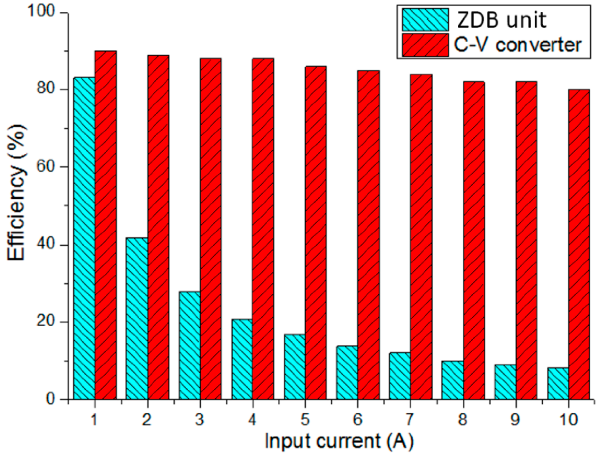
To illustrate the advantage of the proposed design, the zener diodes typed 1N3311 are used to compare with the prototype. The reverse bias voltage of the diodes is 12 V, and the rated power dissipation is 50 W. To avoid the overheating or damage of diodes, three diodes connected in parallel are used to form a ZDB power-supply module. Then a resistive load is parallel connected with the unit as a load and the load power consumption is 10 W. Then the comparison on the efficiencies of the ZDB module and the prototype under different currents is illustrated in Figure 13. It can be seen that the efficiency of the ZDB module decreases obviously with the increasing of the input DC line current. By contrast, the efficiency of the prototype only decreases slightly with the increasing of the input current. The conversion efficiency deceasing of the prototype is less than 10% even though the input current varies in a wide range, and the efficiency is above 80% under 10 A current, which is the worst case.
6. Conclusions
This paper has proposed a novel current-to-voltage full-bridge DC-DC converter for feeding power to backbone devices in large-scale cabled seafloor observatories. The detailed model of the converter has been mathematically derived and analyzed. A new duty-cycle-overlap control strategy has been proposed to realize the constant voltage output of the converter. The experimental results have proved the feasibility of the design and showed that much higher efficiency can be achieved under large currents by the proposed converter than the traditional zener-diode-based power supply modules.
Author Contributions
Conceptualization, F.L.; methodology, J.Z. and F.L.; software, J.Z.; validation, F.L.; formal analysis, J.Z.; investigation, J.Z. and F.L.; resources, F.L.; writing—original draft preparation, J.Z.; writing—review and editing, J.Z. and F.L.; visualization, J.Z.; supervision, F.L.; funding acquisition, F.L.
Funding
This work was funded by Shanghai science and technology innovation action plan, grant number 16DZ1205000.
Acknowledgments
The authors acknowledge the support of Shanghai Science and Technology Commission for the fund of Shanghai Science and Technology Innovation Action Plan (16DZ1205000). The authors also appreciate reviewers for the constructive comments that helped improve the quality of this manuscript.
Conflicts of Interest
The authors declare no conflict of interest.
References
- Massion, G. Ocean Observing Systems: Vision and Details. In Proceedings of the MTS/IEEE OCEANS 2006, Boston, MA, USA, 18–21 September 2006; pp. 1–6. [Google Scholar]
- Lyu, F.; Zhou, H.; Peng, X.; Yue, J.; Wang, P. Technical preparation and prototype development for long-term cabled seafloor observatories in Chinese marginal seas. In SEAFLOOR OBSERVATORIES: A New Vision of the Earth from the Abyss; Favali, P., Beranzoli, L., Eds.; Springer: Berlin, Germany, 2015; pp. 503–529. [Google Scholar]
- Lyu, F.; Zhou, H.; Yue, J.; He, B. Power system structure and topology reliability of cabled seafloor observatory networks. J. Tongji Univ. (Nat. Sci.) 2014, 42, 1604–1610. [Google Scholar]
- Lyu, F.; Peng, X.; Zhou, H.; Yue, J.; He, B. Design of a prototype system for cabled seafloor observatory networks. Chin. J. Sci. Instrum. 2012, 33, 1134–1140. [Google Scholar]
- Howe, B.M.; Duennebier, F.K.; Lukas, R. The ALOHA Cabled Observatory. In SEAFLOOR OBSERVATORIES: A New Vision of the Earth from the Abyss; Favali, P., Beranzoli, L., Eds.; Springer: Berlin, Germany, 2015; pp. 439–463. [Google Scholar]
- Howe, B.M.; Kirkham, H. Power System Considerations for Undersea Observatories. IEEE J. Ocean. Eng. 2002, 27, 267–274. [Google Scholar] [CrossRef]
- El Forjani, M.; Hashem, Z. Detection of fault location, monitoring and control in underwater power system. In Proceedings of the Power Engineering Conference, Dublin, Ireland, 2–5 September 2013; pp. 1–6. [Google Scholar]
- Aghaebrahimi, M.R.; Menzies, R.W. Small power tapping from HVDC transmission systems: A novel approach. IEEE Trans. Power Deliv. 1997, 12, 1698–1703. [Google Scholar] [CrossRef]
- Ekstrom, A.; Lamell, P. HVDC tapping station: Power tapping from a DC transmission line to a local AC network. In Proceedings of the International Conference on AC and DC Power Transmission, London, UK, 17–20 September 1991; pp. 126–131. [Google Scholar]
- Bahram, M.; Baker, M.; Bowles, J.; Bunch, R.; Lemay, J.; Long, W.; McConnach, J.; Menzies, R.; Reeve, J.; Szechtman, M. Integration of small taps into (existing) HVDC links. IEEE Trans. Power Deliv. 1995, 10, 1699–1706. [Google Scholar] [CrossRef]
- Asakawa, K.; Kojima, J.; Muramatsu, J.; Takada, T.; Kawaguchi, K.; Mikada, H. Current-to-Current Converter for Scientific Underwater Cable Networks. IEEE J. Ocean. Eng. 2007, 32, 584–592. [Google Scholar] [CrossRef]
- Redl, R.; Sokal, N.O. Push-pull current-fed multiple-output dc/dc power converter with only one inductor and with 0 to 100% switch duty ratio. In Proceedings of the IEEE Power Electronics Specialists Conference, Atlanta, GA, USA, 16–20 June 1980; pp. 341–345. [Google Scholar]
- Yakushev, V.; Meleshin, V.; Fraidlin, S. Full-Bridge Isolated Current Fed Converter with Active Clamp. In Proceedings of the Applied Power Electronics Conference & Exposition IEEE, Dallas, TX, USA, 14–18 March 1999; pp. 560–566. [Google Scholar]
- Wolfs, P.J. A current-sourced DC-DC converter derived via the duality principle from the half-bridge converter. IEEE Trans. Ind. Electron. 1993, 40, 139–144. [Google Scholar] [CrossRef]
- Kawaguchi, K.; Kaneko, S.; Nishida, T.; Komine, T. Construction of the DONET real-time seafloor observatory for earthquakes and tsunami monitoring. In SEAFLOOR OBSERVATORIES: A New Vision of the Earth from the Abyss; Favali, P., Beranzoli, L., Eds.; Springer: Berlin, Germany, 2015; pp. 211–228. [Google Scholar]
- Lu, S. Infrastructure, Operations, and Circuits Design of an Undersea Power System. Ph.D. Thesis, University of Washington, Seattle, WA, USA, 2006. [Google Scholar]
Figure 1.
The system structure of seafloor observatories [4].
Figure 1.
The system structure of seafloor observatories [4].

Figure 2.
Two types of power systems in cabled seafloor observatories (CSOs). (a) Constant-current power-feeding system. (b) Constant-voltage power-feeding system.
Figure 2.
Two types of power systems in cabled seafloor observatories (CSOs). (a) Constant-current power-feeding system. (b) Constant-voltage power-feeding system.
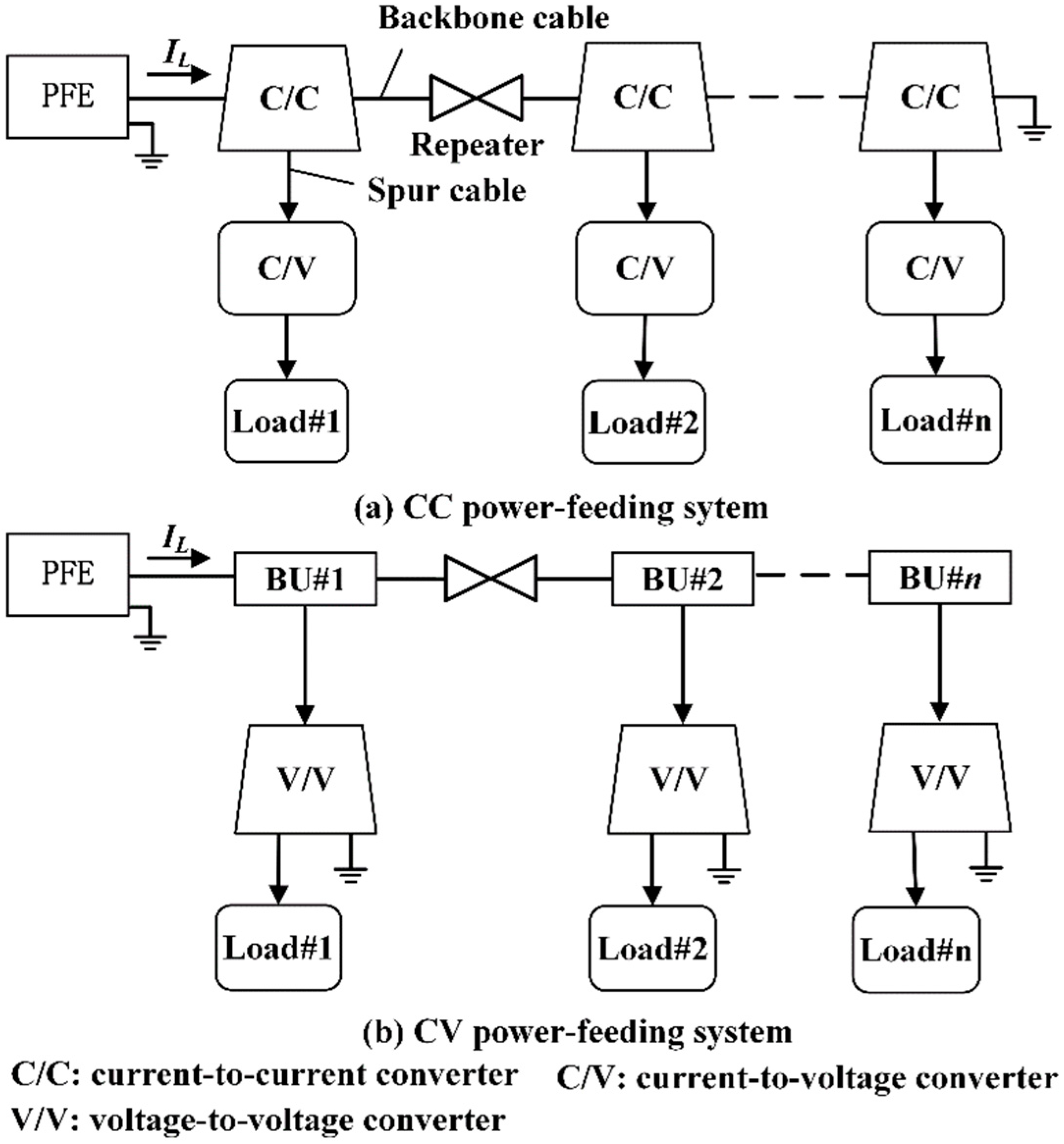
Figure 3.
Startup operation of the current-to-voltage converter.

Figure 4.
Circuit topology of the current-to-voltage converter.
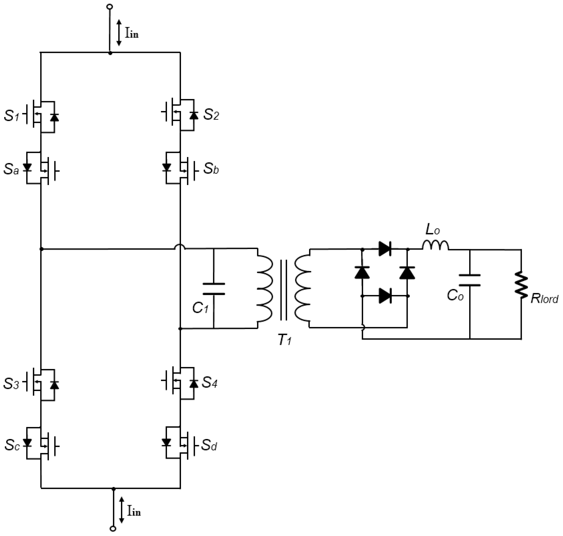
Figure 5.
The equivalent power conversion circuit: (a) Under no-load condition; (b) under loading condition.
Figure 5.
The equivalent power conversion circuit: (a) Under no-load condition; (b) under loading condition.

Figure 6.
Three operating modes of the current-to-voltage converter. (a) Mode 1 (charging). (b) Mode 2 (no-charging). (c) Mode 3 (reverse charging).
Figure 6.
Three operating modes of the current-to-voltage converter. (a) Mode 1 (charging). (b) Mode 2 (no-charging). (c) Mode 3 (reverse charging).
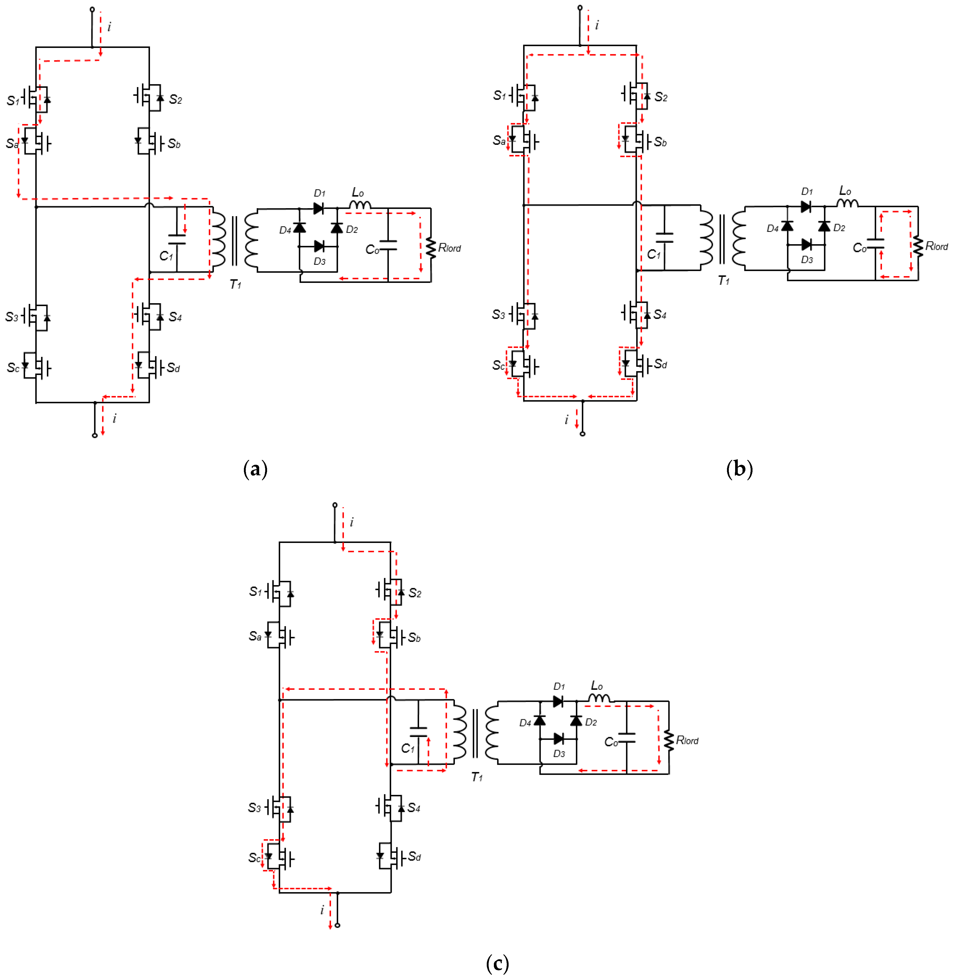
Figure 7.
The design to adjust the turn ratio of the transformer of the proposed converter.
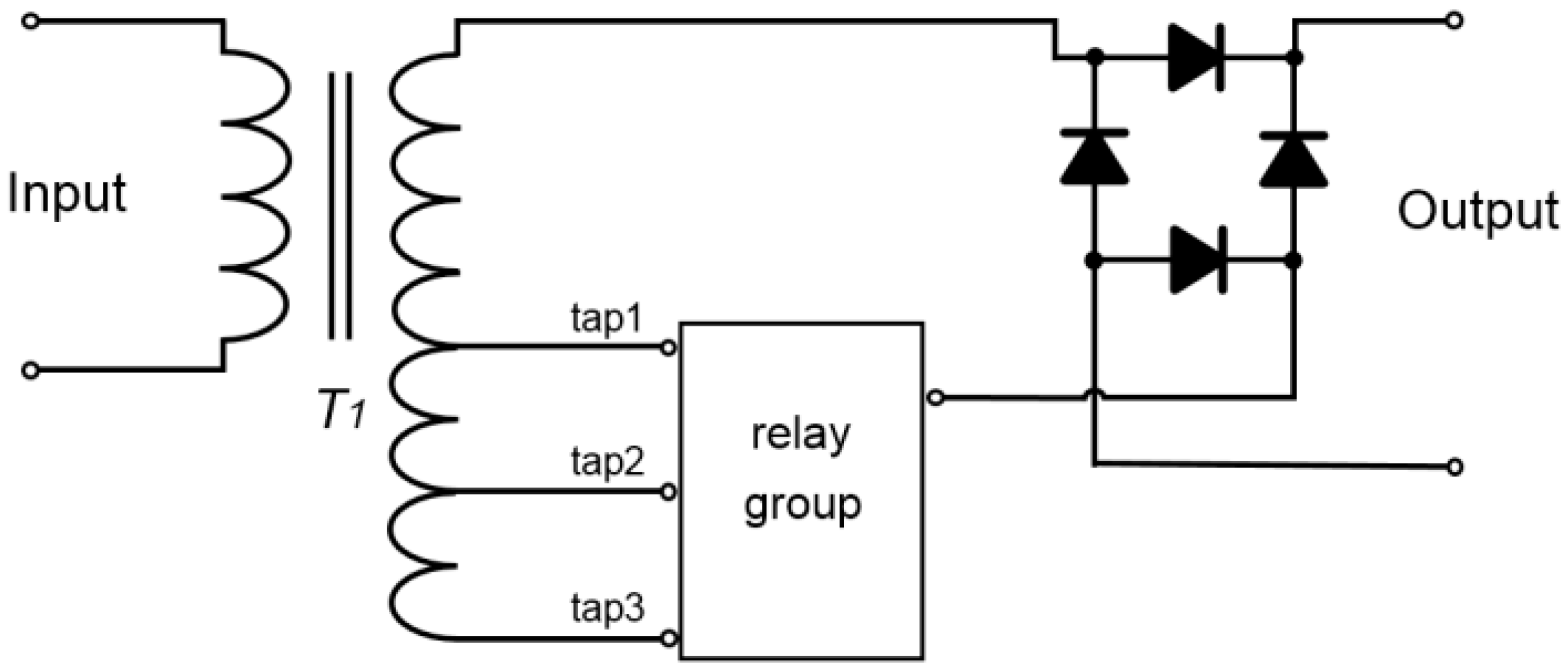
Figure 8.
(a) The block diagram of the experimental setup; (b) the photograph of the experimental setup.
Figure 8.
(a) The block diagram of the experimental setup; (b) the photograph of the experimental setup.

Figure 9.
(a) The AC voltage across C1. (b) The voltage stress across the switch. (c) The output voltage across the load when the prototype starts up. (d) The ripple of the output voltage.
Figure 9.
(a) The AC voltage across C1. (b) The voltage stress across the switch. (c) The output voltage across the load when the prototype starts up. (d) The ripple of the output voltage.
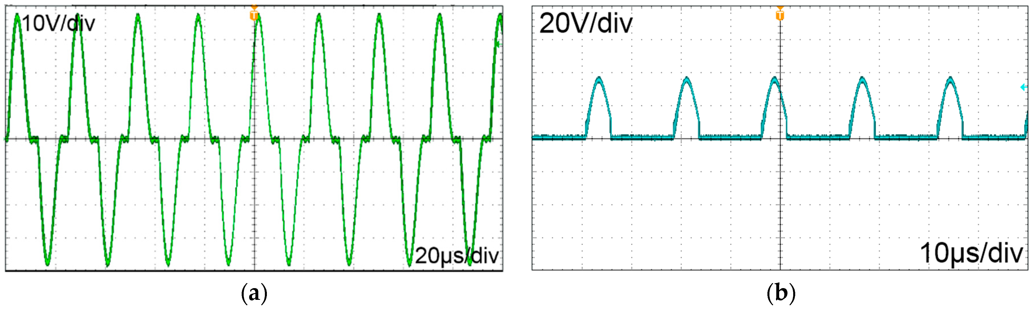
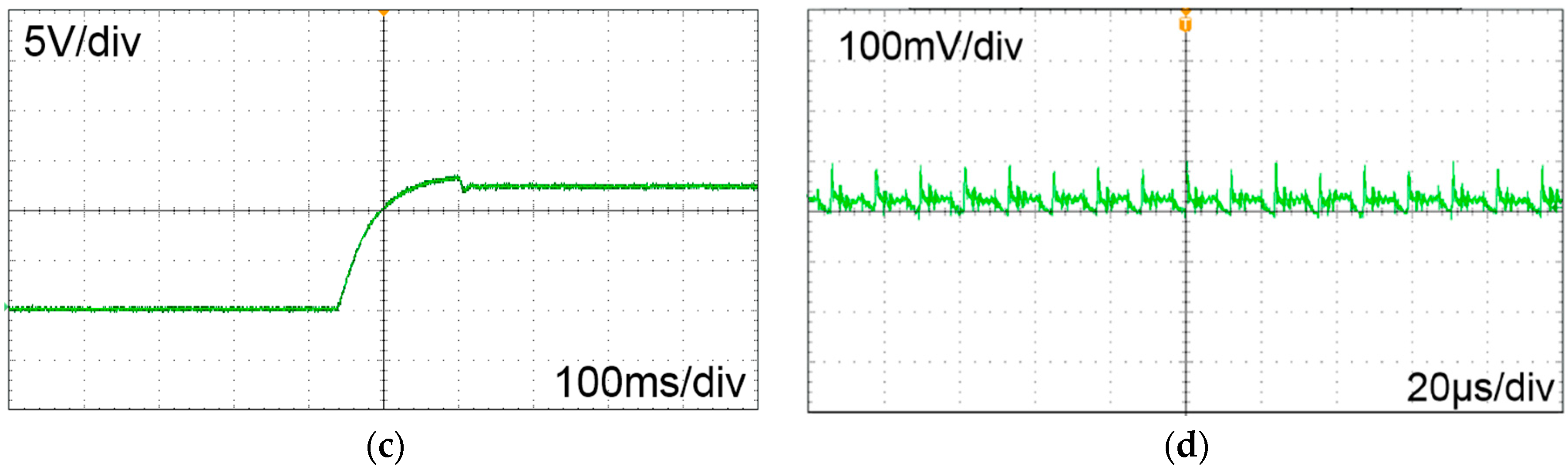
Figure 10.
The dynamic voltage and current waveforms of the output diode (a) and the inductor (b).

Figure 11.
(a) The output voltage under the alteration of input current. (b) The output voltage under the alteration of the load. (c) The output voltage under the adjusting of the turn ratio.
Figure 11.
(a) The output voltage under the alteration of input current. (b) The output voltage under the alteration of the load. (c) The output voltage under the adjusting of the turn ratio.

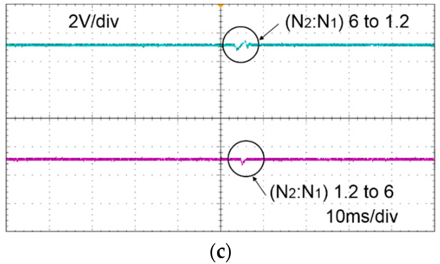
Figure 12.
Three-dimensional curves of the efficiency under different current and turn ratio conditions.
Figure 12.
Three-dimensional curves of the efficiency under different current and turn ratio conditions.

Figure 13.
Comparison on the efficiency of the zener-diodes-based module and the prototype under different input direct current (DC) line currents.
Figure 13.
Comparison on the efficiency of the zener-diodes-based module and the prototype under different input direct current (DC) line currents.

Table 1.
Parameters of the prototype.
| Parameters | Values |
|---|---|
| Input current | 1–10 A |
| Output voltage | 12 V |
| Rated output power | 10 W |
| Capacitor C1 | 0.47 μF |
| Switching frequency | 40 kHz |
| Taps number | 10 |
| Minimum turn ratio | 1.2 |
| Maximum turn ratio | 12 |
© 2019 by the authors. Licensee MDPI, Basel, Switzerland. This article is an open access article distributed under the terms and conditions of the Creative Commons Attribution (CC BY) license (http://creativecommons.org/licenses/by/4.0/).
Share and Cite
MDPI and ACS Style
Zhu, J.; Lyu, F. A Current-to-Voltage DC-DC Converter for Powering Backbone Devices of Scientific Cabled Seafloor Observatories. Energies 2019, 12, 2261. https://doi.org/10.3390/en12122261
AMA Style
Zhu J, Lyu F. A Current-to-Voltage DC-DC Converter for Powering Backbone Devices of Scientific Cabled Seafloor Observatories. Energies. 2019; 12(12):2261. https://doi.org/10.3390/en12122261
Chicago/Turabian StyleZhu, Jiayu, and Feng Lyu. 2019. "A Current-to-Voltage DC-DC Converter for Powering Backbone Devices of Scientific Cabled Seafloor Observatories" Energies 12, no. 12: 2261. https://doi.org/10.3390/en12122261
Note that from the first issue of 2016, this journal uses article numbers instead of page numbers. See further details here.