1. Introduction
Nowadays, the Modular Multilevel Converter (MMC) has become a promising solution in different applications, such as in High Voltage Direct Current (HVDC) [
1,
2], high-power motor drivers [
3,
4] and STATic COMpensators (STATCOM) [
5,
6]. Thanks to several advantages, such as high modularity, scalability, low Total Harmonic Distortion (THD), high efficiency and high reliability, the interest in this topology has increased in both industry and academy [
7]. However, this topology presents several challenges, such as the necessity to control the circulating current, ensure the balance of the losses among the Sub-Modules (SMs) and maintain the capacitor voltage balanced [
8]. In the literature, two Capacitor Voltage Balancing (CVB) control algorithms are mainly proposed: the individual control approach [
9] and the global arm control approach. The latter is commonly used in the Nearest Level Control (NLC) which requires a Sorting Algorithm (SA) [
10]. Indeed, to balance the capacitor voltages (CVs), the SMs with the highest or lowest CV must be selected based on the arm current direction. Then, the SA provides a sorted list of the SMs according to their capacitor voltages.
In MMC applications, the implementation of SAs is a key challenge mainly due to the timing performances and the high computation efforts of this kind of algorithms. Low timing performances can slow down the CVB algorithm by limiting either the maximum sampling frequency or the maximum allowable number of SMs in the converter. The SAs are usually implemented in microcontrollers or in digital signal processors due to their easy implementation. However, they are based on loop/recursive operation leading to a significant increase of the execution time when the number of SMs grows. Some authors propose max/min approaches to overcome this issue [
11,
12,
13]. Such methods suppose that only one SM has to be inserted/bypassed in the next sampling instant. Then, they only find the SM with the maximum (or minimum) CV by achieving a strong reduction of the execution time. However, in the case of faults or when the capacitors are approaching the maximum allowable voltage, more SMs need to be inserted or bypassed at the same time. The max/min algorithms then require more sampling periods to insert or bypass the required SMs, which leads to slow converter dynamic performance. A solution could be to run multiple times the max/min method within the same sampling instant; however, this choice increases the whole execution time by leading to the same problem highlighted for the bubble SA.
For the above-mentioned reasons, a hardware implementation of a sorting method has been proposed in this paper. Several studies have confirmed that the Field-Programmable Gate Array (FPGA) technology is really promising in industrial control applications [
14]. Such platforms are more and more used in industry and in academia for achieving high timing performance, which is difficult to reach with the software counterpart. Since the FPGAs are able to exploit the inherent parallelism of the algorithm, they lead to a significant reduction of the execution time. Moreover, they are often used in MMC applications due to the possibility: to drive a huge amount of SMs [
15], to implement fast protections, to interface more ADC modules [
16], to implement real-time emulator [
17] and for fast communication [
18].
Among the different hardware implementations of sorting approaches, the Sorting Networks (SNs) have been chosen to be implemented in FPGA due to their inherent parallelism and enhanced timing performance [
19]. The Bitonic SN has been considered due to its low resource requirement and its modular structure [
20]. The authors in [
20] compared this SN with the Odd-Even SN. However, the main aim was to provide a method for pre-evaluating the hardware resources and the execution time of the network. No simulations or hardware-in-the-loop results were provided, and no justifications were given for the use of these networks in MMC. In this work, instead, some simulation results are shown in normal and faulty conditions to highlight the benefits of adopting an algorithm that provides a complete sorted list with respect to one that only gives the SM with the highest (lowest) capacitor voltage. Another contribution of this work is the study of the achievable trade-offs between the execution time and the required resources when this kind of sorting methods are implemented for MMC applications. For this aim, three kinds of FPGA implementations are presented: a fully pipelined architecture, a hybrid structure and a fully factorized SN. In this way, designers can choose the proper solution for their requirements to achieve the best compromise between the required timing performance and the available resources. After having chosen the right solution that fits the requirements of the MMC application considered in this work, the SN architecture is compared with the classical bubble sorting algorithm and the max/min approach in terms of execution time. To demonstrate the feasibility of the proposed architecture, a Hardware-In-the-Loop (HIL) validation is also made.
The paper is divided as follows: firstly, an MMC overview is given along with its control hierarchy. Then, the Bitonic SN is presented and its peculiar aspects in MMC applications are treated.
Section 4 presents the simulation results in normal and faulty conditions. After that, different FPGA implementations are proposed and compared in terms of required resources and execution time in
Section 5. Then, the chosen hardware implementation is compared with the software implementation of both the classical bubble SA and the max/min approach. HIL results for a single-phase 32-SM MMC are given to demonstrate the effectiveness of the proposed SN implementation. Finally, conclusions are drawn.
3. Description of the Sorting Networks
The sorting networks are widely adopted in data processing [
19] due to their timing performance. They consist of a fixed parallel structure composed of m-horizontal wires and several Compare-and-Swap (CS) operators. The latter carries out the sorting of two input elements: it compares them and ensures that the larger input value comes out from the upper output wire and the smaller input from the lower wire. Among the different SNs, the Bitonic structure is chosen in this work due to its modular aspect and to the reduced amount of CS operators [
19,
20].
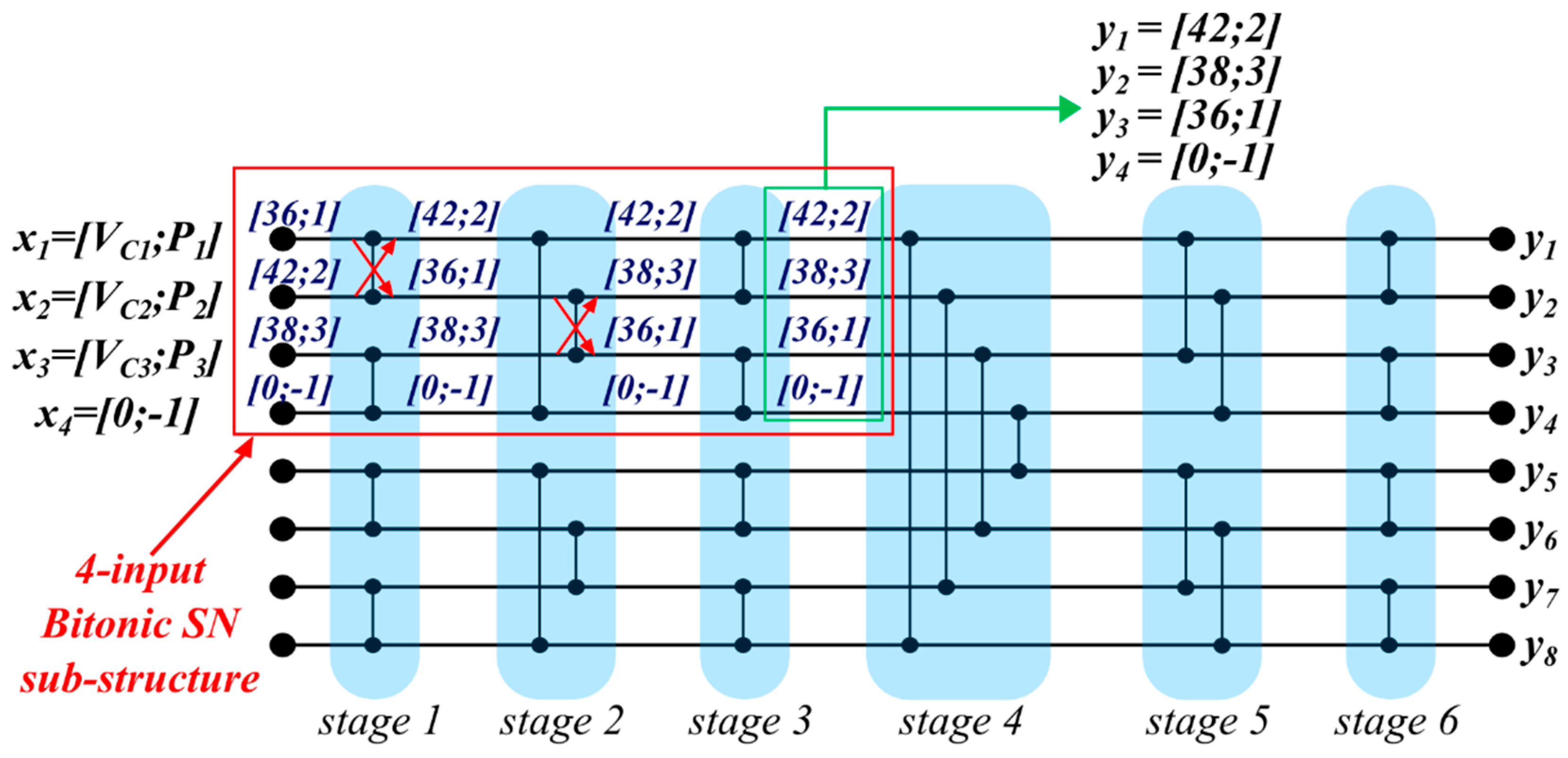
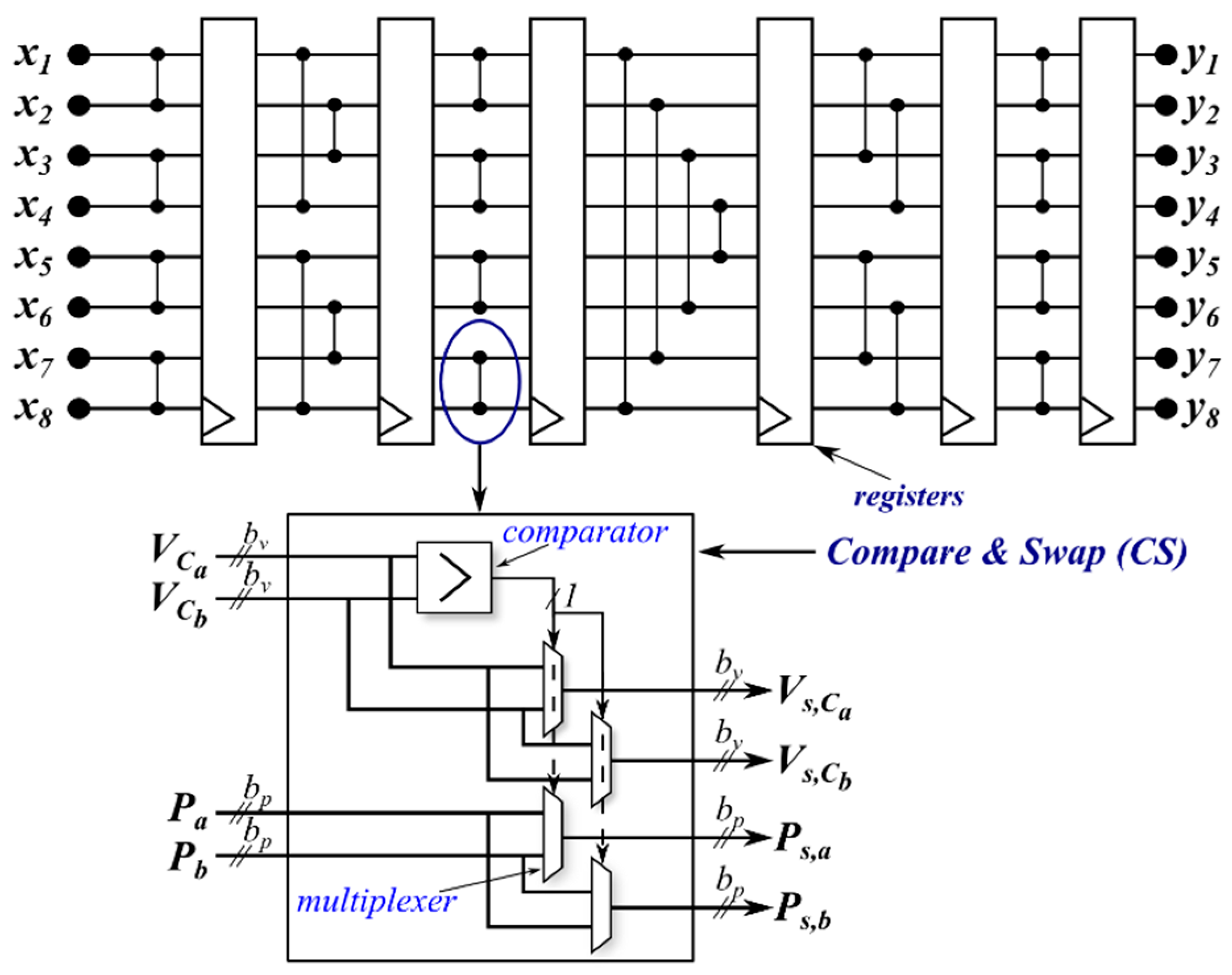
Such a sorting network is composed of different stages which in turn are composed by several CS operators. In
Figure 4, an eight-input Bitonic Sorting Network is depicted. In this case, six stages in the structure can be highlighted. The number of stages obviously depends on the number of the input. The unsorted sequence, denoted with
x, is applied on the left, and the sorted list
y results on the right. Only one element per wire can be applied.
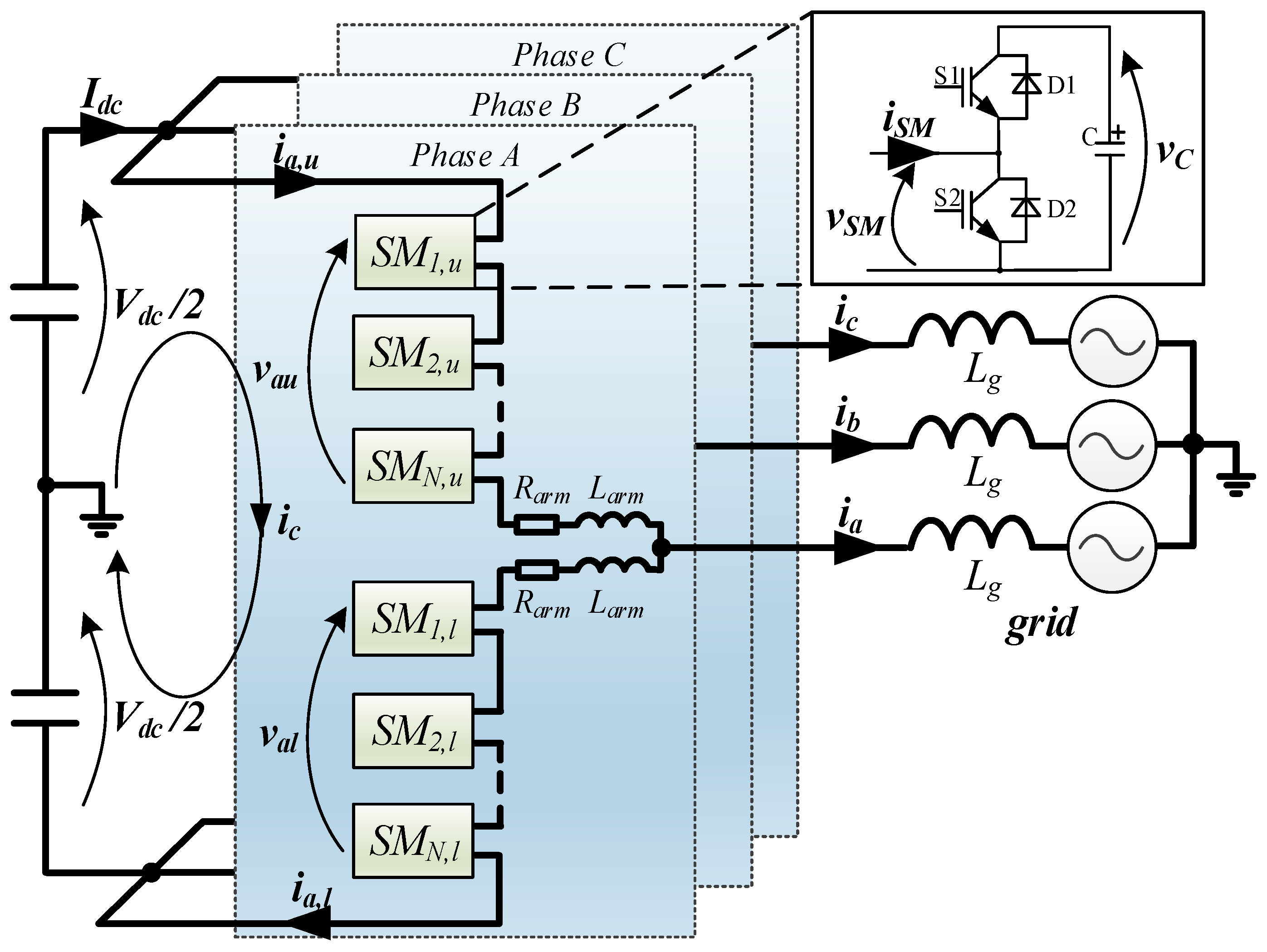
Firstly, each SM is enumerated starting from the top of each arm, as shown in
Figure 1, and its position is named here
. Each element
xi must consist of the acquired capacitor voltage
and the corresponding position
, as depicted in
Figure 4, where the subscript pm has been omitted for simplicity. A comparison of the capacitor voltages is performed and the swap operation is executed for both
and
if the voltages are not in the right order. The output
y results in a sorted list with the voltages in ascending order along with the corresponding physical SM position. Then, if the SM with the highest voltage is needed for insertion, the first element
is considered; otherwise, the last one is selected.
Another aspect that should be considered is the length of the list. Indeed, in MMC applications, the modularity is one of the main advantages [
7]. It consists in the possibility to raise the power rating by adding more SMs in the arm. This means that the number of SMs, and then the length of the list, is not known a priori. However, a maximum number of SMs in an arm (named here with M) can always be presumed and then the SN is built for this worst-case scenario. In these conditions, some elements of the list can be left empty since the actual length of the list N can be different from M. To guarantee the proper behavior of the SN, these dummy elements have to be filled by setting the voltage equal to 0 and the position to −1 [
20]. Therefore, these elements are kept in the last positions and the elements with positions different from −1 are selected when the SMs with lowest voltages are required.
An example of an eight-input Bitonic SN for a MMC with three SMs per arm (
and
) is depicted in
Figure 4. The dummy element is in Position 4 and it is kept in that position along the net. The result can be achieved before the last stage by considering only a sub-structure of the network as shown in the example. After having presented the SNs and having discussed their main peculiar aspects in MMC applications, some simulation results are shown in the next section.
4. Simulation Results
In this section, the Bitonic SN is compared with the max/min approach to show the differences between an algorithm that completely sorts the list and one that searches only the SM with the highest/lowest CV. The simulations have been performed in PLECS
® power electronic simulation environment in both normal and faulty conditions. The MMC and grid parameters are given in
Table 1 and
Table 2, respectively.
The Bitonic SN and the max/min approach have been implemented in PLECS. It is worth to note that the SN is intrinsically parallel; to simulate it its treatment has been serialized. Thus, its behavior is equal to the one achieved with a classical sorting algorithm such as the BSA. A tolerance band has also been introduced as shown in [
23]. The max/min method proposed in [
13] has been adopted in this work. The tolerance bands are set to 2 kV.
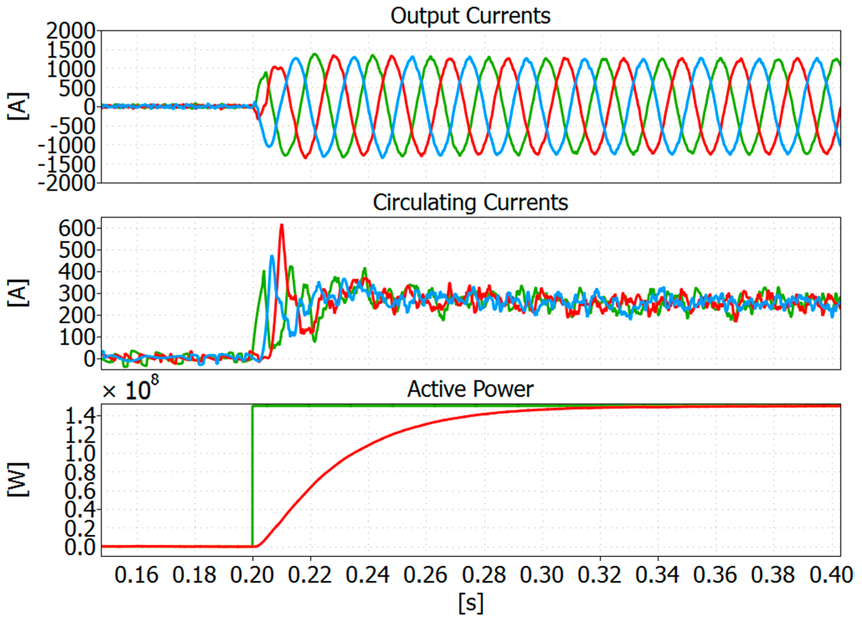
4.1. Normal Condition
The simulation results shown in this section were achieved during steady state condition, i.e., without any faults in the system. At 0.2 s, the converter starts to deliver power to the grid. In
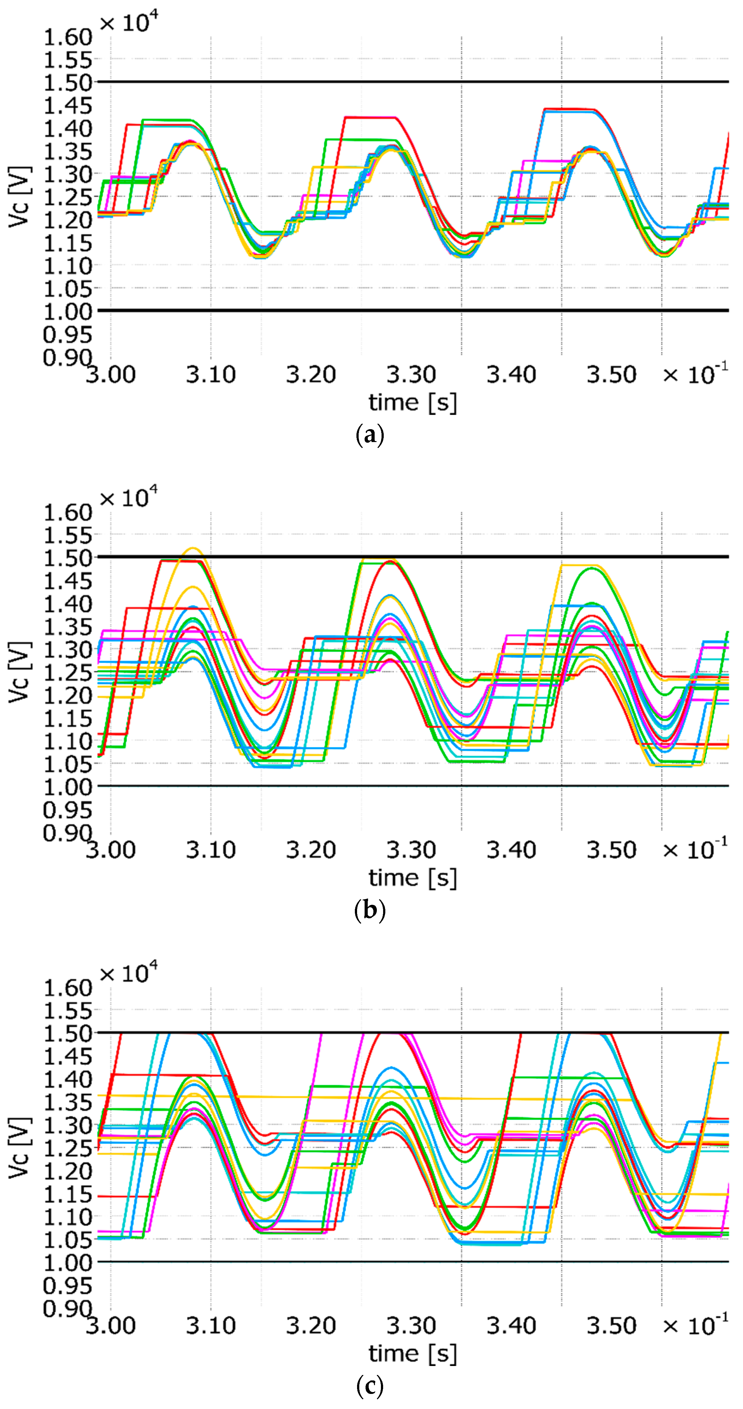
Figure 5, the output currents, circulating currents and active power are shown when the Bitonic SN is adopted. The capacitor voltages for both the Bitonic SN and the max/min approach are depicted in
Figure 6.
When the best SMs are always selected, the algorithm that provides the complete sorted list achieves a better balance in comparison with the max/min approach. However, it leads to a high switching frequency, equal to 409 Hz in the studied case (
Figure 6a). The max/min approach instead only selects one SM to be inserted or bypassed when a change in
is resulted from the NLC (
Figure 6b). Then, the switching frequency is intrinsically optimized and almost equal to 60 Hz. By adopting the improved
fsw for the Bitonic SN, as described in
Figure 3, the
fsw can be reduced. In this case, it is comparable to the one achieved with the max/min method, but the achieved balance is worse than the one achieved without the
fsw optimization, as shown in
Figure 6c.
Finally, it can be concluded that in normal condition and when the fsw optimization is active, the max/min method and the sorting algorithm give almost the same balancing results and switching frequency. From now on, the fsw optimization is considered active, if not differently mentioned.
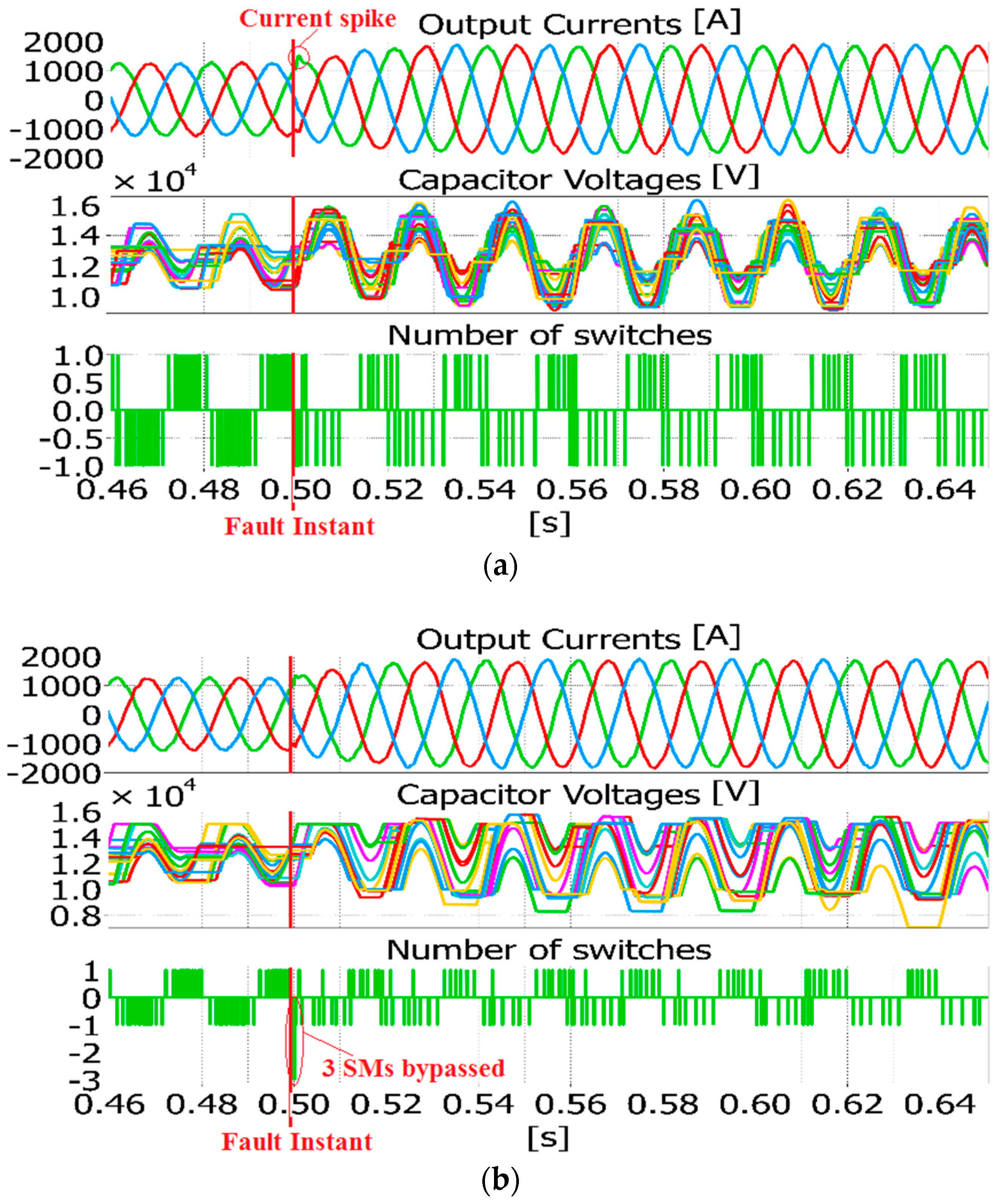
4.2. Phase-to-Ground Fault
The phase-to-ground fault is simulated by adopting the previous MMC and grid parameters. When this kind of fault appears in the system, the control algorithm demands more SMs to be inserted or bypassed in the same sampling period. The fault is applied at 0.5 s on the phase
a.
Figure 7 shows the output currents, the capacitor voltages of phase
a and the number of switches for the same phase. When the number of switches is positive, it means that the SMs have been inserted, while, when it is negative, the SMs have been bypassed. It is worth noting that, in the case of the SN, three SMs have been bypassed at the moment of the fault. This number can relatively increase if the number of SMs in the arm is higher. The possibility to apply the required changes in one sampling period
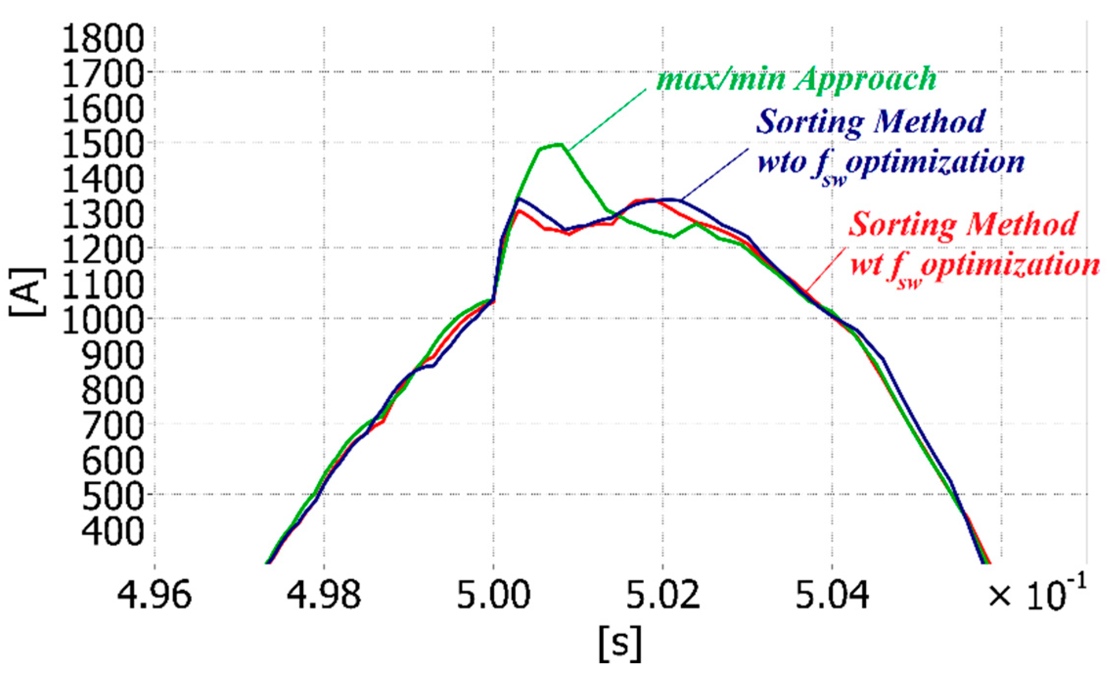
Ts enhances the dynamic performance of the controller. Indeed, at the fault instant, the algorithms that provide the fully sorted list are able to track the current reference and avoid spikes on the output current as shown in
Figure 8.
On the other hand, the max/min method keeps only one switch per each
Ts, requiring more sampling periods to insert/bypass the needed SMs. This leads to a lower controller dynamic that provokes a spike on the output current, as depicted in
Figure 8. It is also possible to run the max/min method several times in the same sampling period to get the required SMs, but this leads to a longer execution time that can easily exceed the chosen
Ts, not guaranteeing the proper controller behavior.
The advantages of the proposed SN over the min/max approach have been demonstrated and the FPGA implementation of the Bitonic SN is now dealt with.
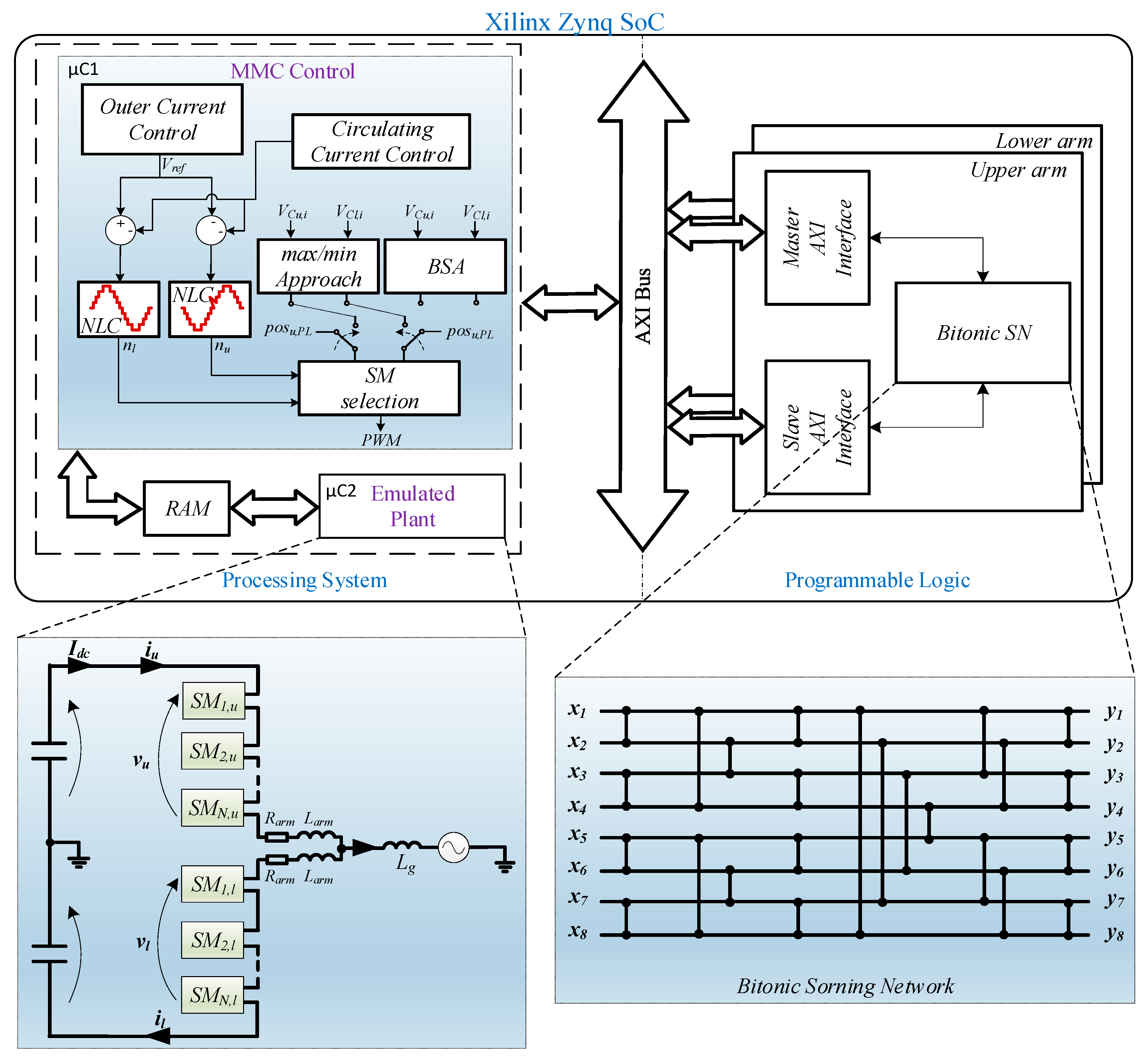
5. FPGA Implementation of the Bitonic SN
Different FPGA-based implementations of SNs are shown and compared in this section. Firstly, the fully pipelined SN is presented. After that, a hybrid structure and a fully factorized SN are proposed for reducing the required resources. Finally, they are compared in terms of required resources and latency, i.e., the number of system clock cycles for achieving the final result.
5.1. Fully Pipelined SN
This kind of implementation of the SN allows a drastic reduction of the execution time. This architecture is driven by an external clock signal that synchronizes the data through the SN. After each stage, a bank of flip-flops is allocated for storing the results of CS operators, as shown in
Figure 9. A new list of CVs can be fed to the input of the SN every clock cycle. The basic structure of the CS operator is also presented in
Figure 9. It consists of a comparator and four multiplexers. The inputs are the two SM capacitor voltages
and
and the two SM positions
Pa and
Pb. The outputs are the sorted capacitor voltages
and
and their corresponding positions
Ps,a and
Ps,b. The values of
bv and
bp correspond to the size of the fixed-point format of the voltage and of the position, respectively.
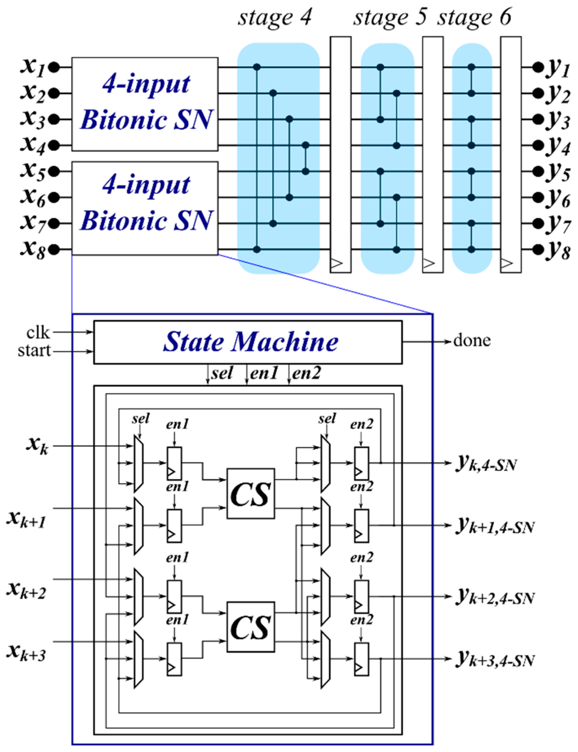
5.2. M-Factorized SN
To reduce the required number of CS operators, the previous SN structure can be factorized. The objective is to reuse a single CS operator to perform more CS operations. However, this optimization leads to an increase of the latency in the architecture. Then, a compromise between the factorization level, i.e., which sub-structure of the Bitonic SN is factorized, and the latency is necessary.
Figure 10 shows an example using
and the factorization level
L equal to 4. This means that the four-input Bitonic SN sub-structure, highlighted in
Figure 4, is factorized.
This solution allows a reduction of the required CS operators and, therefore, the used resources. Indeed, the factorized four-input Bitonic SN only requires two CS operators instead of six. However, the latency will be 6 instead of 3 and no other list can be inserted at the input during this calculation, reducing the throughput of the architecture. It is worth noting that this solution also requires eight Multiplexers.
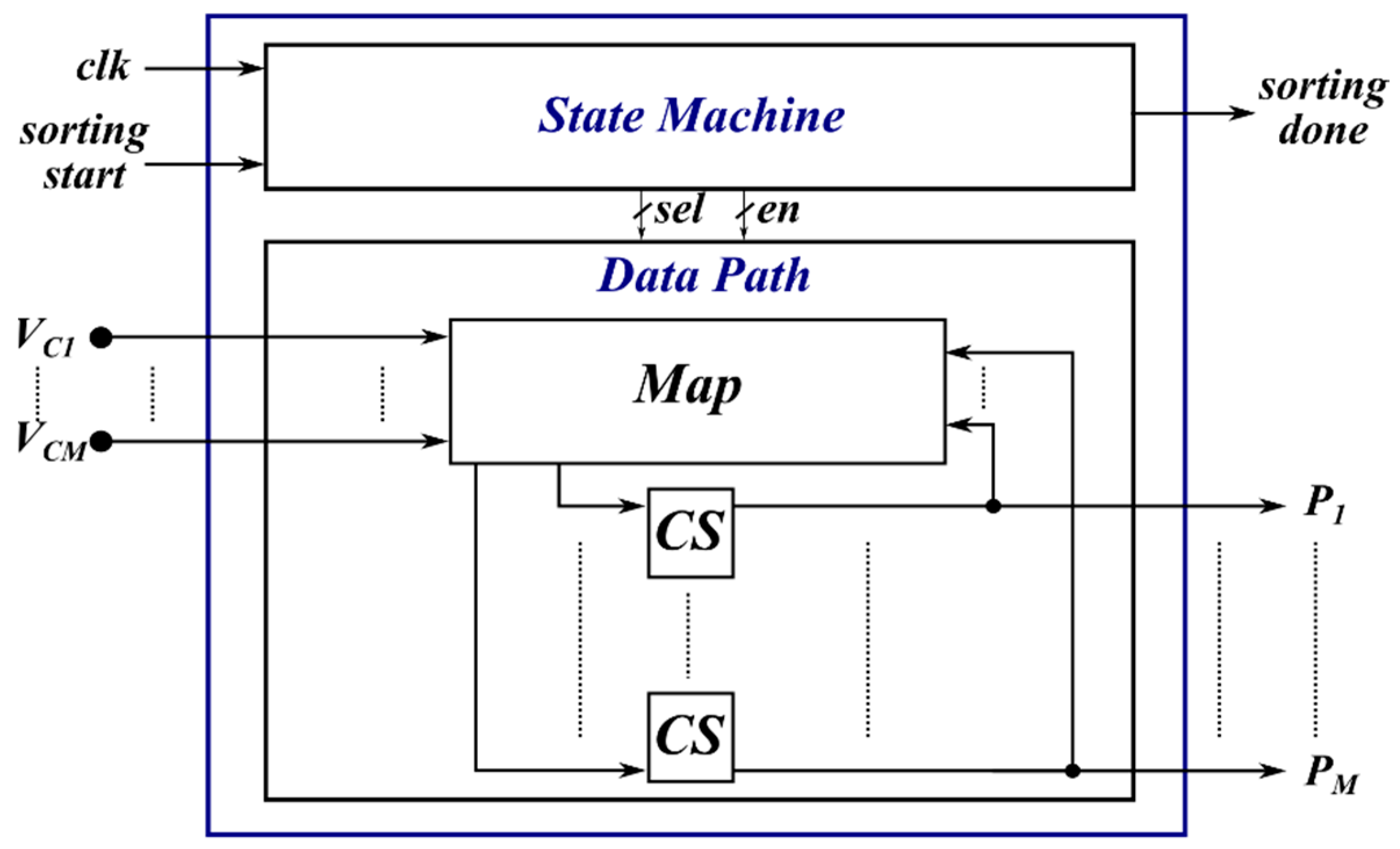
5.3. Fully Factorized SN
The last proposed architecture is the fully factorized SN, i.e., . This alternative can be adopted to drastically reduce the required resources at the cost of a larger latency.
This architecture is depicted in
Figure 11. The state machine generates and sends the synchronization signals to the data path which processes the input data. The Map operator implements the multiplexers and the registers needed for the factorization. The sorting done signal is raised when the sorted list is available at the output.
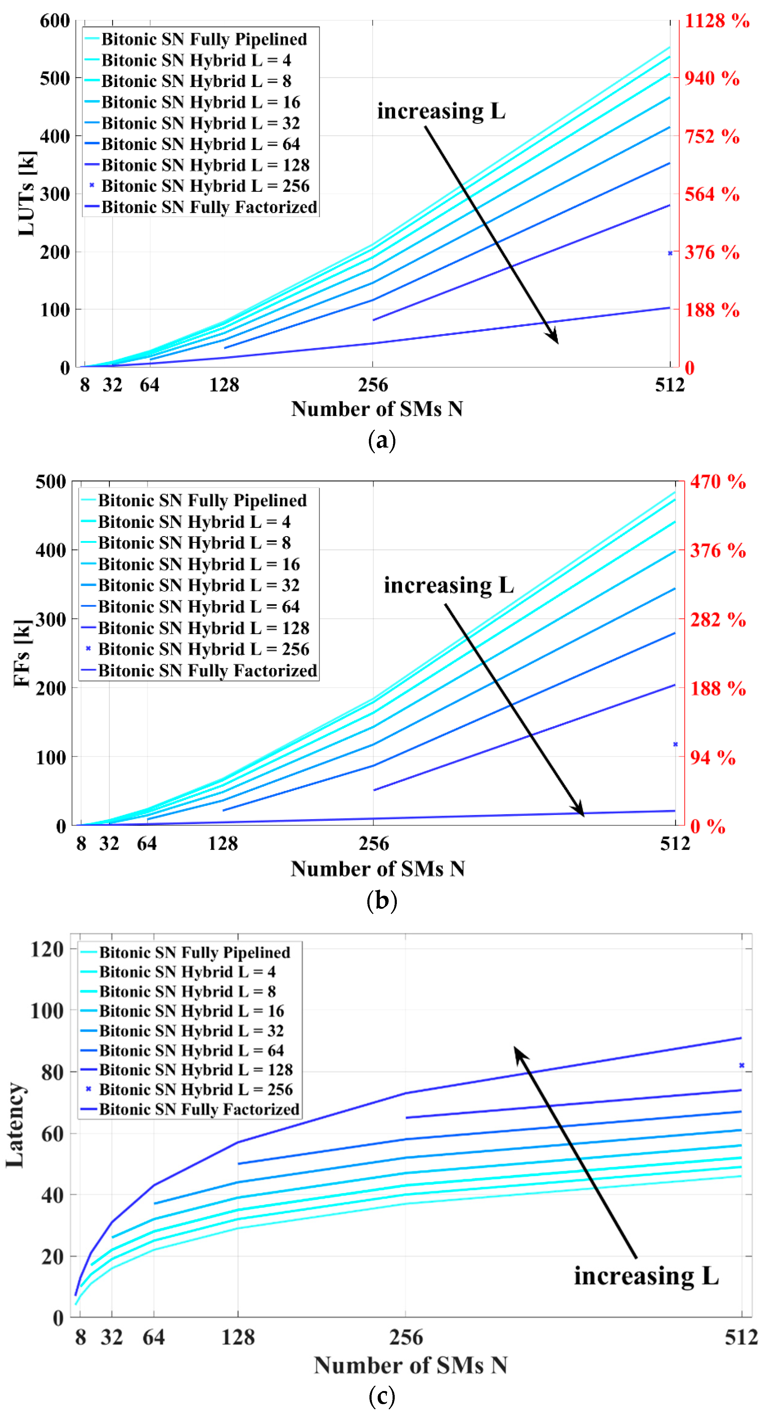
5.4. Comparison
In this section, the previous SN structures are compared in terms of five-input Look-Up-Tables (LUTs), Flip-Flops (FFs) and latency. The LUTs, FFs and latency for these structures can be easily pre-evaluated, as shown in [
20].
Figure 12a depicts the required LUTs with different factorization level. It is shown that, by increasing the number of SMs,
N, the required LUTs increase. The fully pipelined is the structure that requires the highest amount of LUTs, as expected. By increasing the factorization level, the needed LUTs can be reduced. The right
y axis shows the percentage of the required LUT when the selected low-cost System-on-Chip (SoC) device is considered. Then, it is obvious that a fully pipelined structure for high numbers of
N is impracticable with this kind of device. The same happen for the FFs, as depicted in
Figure 12b. On the other side, a higher factorization level leads a higher latency number, as shown in
Figure 12c. Thus, a compromise is required between the LUTs, FFs and latency. The designer can then pre-evaluate the required resources and the latency to choose the best solution for its requirements.
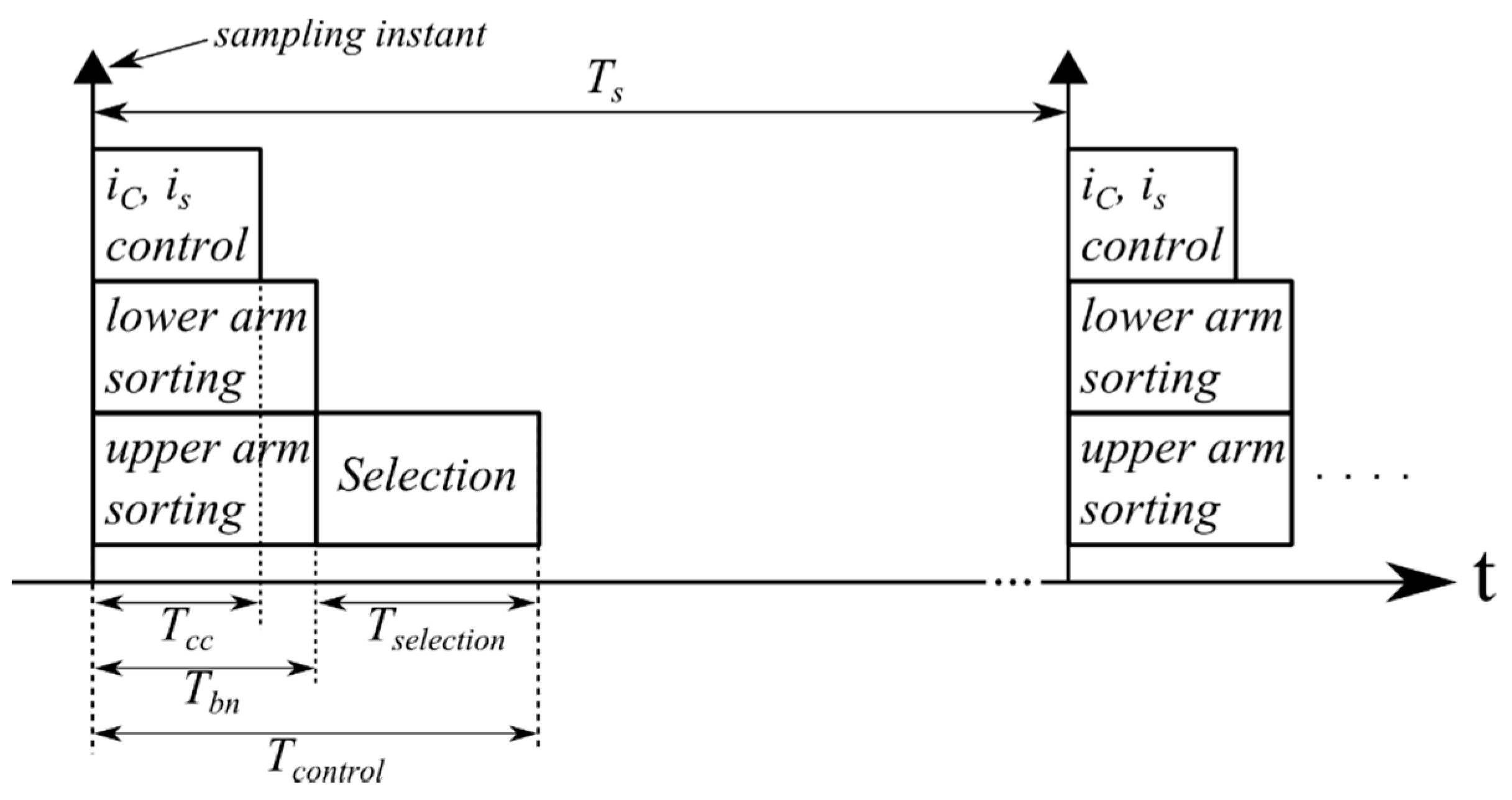
5.5. Timing Diagram
In this section, the timing diagram for the proposed Bitonic SN is presented in
Figure 13. The following control actions can be executed in parallel: the current controls (for both the output current
is and the circulating current
ic), the upper arm sorting and the lower arm sorting. This leads a reduction of the whole control time
Tcontrol. The latter is the sum of two contributions: (a) the longer time between the current control time
Tcc and the time needed to the Bitonic SN
Tbn; and (b) the time
Tselection needed for selecting the SM to be inserted. From Equation (3) and
Figure 13, it is possible to derive the maximum sorting time
Tmax,sort that has to be guaranteed:
6. Hardware-In-the-Loop Results
A MMC system is usually composed by tens or hundreds of modules per arm. The realization of this kind of systems is very expensive, and then an usual approach is to test the control behavior using HIL approach. In this section, HIL results are provided to validate the proposed sorting method and compare it with the bubble SA and with the max/min approach in terms of the achieved sorting execution time. The Zedboard platform, equipped with a Xilinx SoC Zynq-7020 device (named here as Zynq), has been employed. This device consists of almost 85,000 logic element cells, 4.9 Mb block RAM, 220 DSP and two embedded ARM cortex A9 processors with a clock frequency equal to 667 MHz.
The MMC control, composed by the output current control and the circulating current control, has been implemented in the first ARM core of the Processor System (PS). Along with the MMC control, the bubble sorting algorithm and the max/min approach have been also carried out in the same core. On the other hand, the proposed Bitonic SN has been implemented in the Programmable Logic (PL) side by allowing the implementation of the hardware structures presented in
Section 3 and the adoption of the timing diagram shown in
Figure 13. The fully factorized Bitonic SN structure has been chosen to save hardware resources. In the remaining ARM core, a single-phase MMC model has been emulated based on [
26]. The case of
N = 32 has been considered, which is realistic in view of the industrial implementation of MMC-HVDC by ABB [
27]. A single-phase system has been chosen considering that the performances of the Bitonic SN are identical for the single-phase and the three-phase system. Indeed, in the three-phase case, it can be easily implemented in parallel for achieving the same execution time shown in the following. The adopted capacitor value is 2.4 mF and the output energy is equal to 33 MW. The remaining MMC parameters are shown in
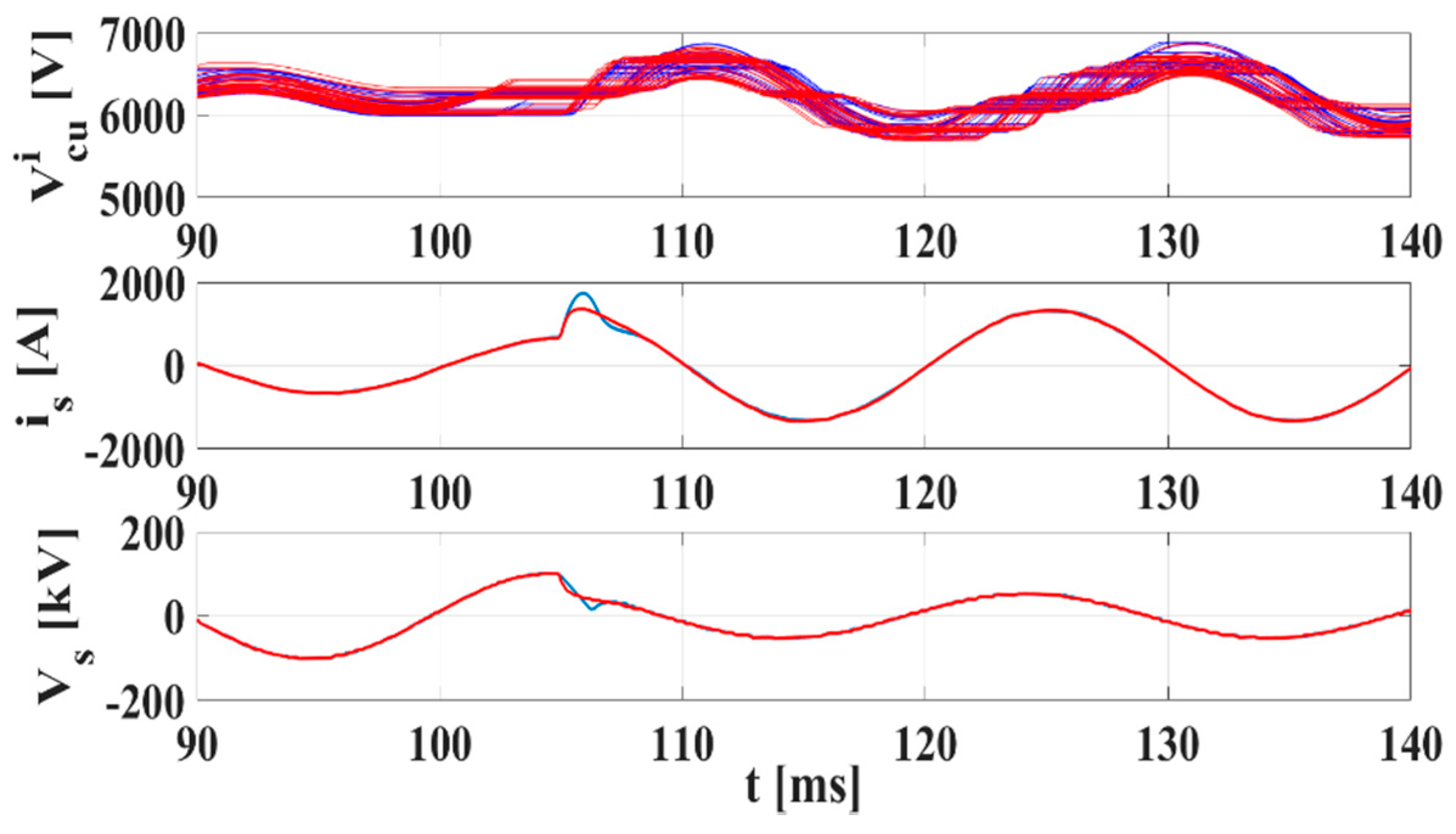
Table 1. The whole implementation structure is depicted in
Figure 14. The internal signals of the board are read and displayed on the PC through a serial communication. A sag voltage of 50% is emulated after 105 ms. The corresponding capacitor voltages, output currents, and output voltages for the max/min approach and the Bitonic SN are shown in
Figure 15.
It is worth noting that the limited dynamic performance of the max/min approach cause an undesired overshoot in
is of about 28%. The achieved execution times for the three techniques in both normal and fault conditions are summarized in
Table 3. The sorting network has been implemented in FPGA and then some operations can be executed in parallel: the current control and the sorting algorithm in this case. Then, the control time is evaluated by summing up the longer execution time between the current control and the sorting algorithm with the selection time.
On the other hand, the bubble SA and the max/min approach have been implemented in the ARM core and then the current control, the sorting algorithm and the selection method are executed in a sequential manner. The whole execution time is then evaluated by summing up all the terms. The bubble SA achieves the worst timing performance by requiring maximum 4.56 µs in normal conditions and 6.46 µs during the emulated fault. It is worth noting that its execution time is not fixed. Thus, it is not deterministic and can be much higher than the ones obtained in this example.
The max/min method needs 2.56 µs and 2.75 µs to be performed in normal and fault conditions, respectively. However, it does not provide a fully sorted list by causing current overshoot during faults. It is important to mention that its execution time is also not fixed. On the other hand, the proposed SN only requires a fixed execution time equal to 0.5 µs. It is also able to provide a fully sorted list useful during fault cases or when more SMs are required (like at the start-up). Its short execution time allows the proper behavior of the controller. However, if the number of SMs increases, the execution time raises and
Ts decreases at the same time. In the case the execution time of the fully factorized structure is higher than the maximum allowable
Ts, it is still possible to adopt either a hybrid structure or the fully pipelined SN that allow a reduction of the execution time. This choice can be done before starting the implementation thanks to the pre-evaluated resources and latency shown in
Section 5 by reducing the time-to-market. Then, the right compromise between the sorting time and the required resources can be ensured.
Table 4 shows the hardware resources required for the implementation of one fully factorized 64-Bitonic SN in the adopted device.
If a three-phase 64-SM MMC is of interest, six Bitonic SN have to be considered and then almost 60% of the available resources are consumed. It is also possible to use only one fully factorized Bitonic SN for accomplishing the sorting of all the arms. Obviously, this solution leads to an increment in the execution time. Another solution can be to implement a fully pipelined Bitonic SN that allows a higher throughput (a new list can be sent after the first stage has been performed) and then a lower execution time at the expense of an increment of the required resources. As already said, the right compromise has to be achieved depending on the case and the discussion in
Section 5 is for this aim.
7. Conclusions
In this paper an FPGA-implementation of the Bitonic Sorting Network for MMC applications has been proposed. The main advantages of the proposed sorting method are: the fixed parallel structure and the possibility to be efficiently implemented in FPGA devices. This leads to a shorter and deterministic execution time, which results in a better performance of the CVB control. Three different architectures have been proposed to meet the different possible requirements of the application of interest: the fully pipelined architecture, the hybrid structure and the fully factorized SN. Their hardware resources and latency have been pre-evaluated and compared. This allows choosing the structure that best fits the application requirements before starting the implementation. Simulation results have been given in both normal and faulty conditions to compare the proposed sorting method with the max/min approach. The latter is considered to request the shortest execution time but it does not provide the fully sorted list by deteriorating the dynamic performance of the controller.
The fully factorized Bitonic SN has been implemented in a low-cost Xilinx Zedboard along with the MMC plant model and the corresponding control. Based on the HIL results, the proposed sorting method shows superior performance. Moreover, the execution time and the output current of the implemented SN have been compared with the ones achieved with the bubble sorting algorithm and the max/min technique in the case of N = 32 and a sag voltage of 50%. The output current obtained with the max/min technique presents an overshoot of about 28% in comparison with the one achieved by adopting an algorithm that provides a fully sorted list. Then, the main gain of the proposed SN compared to the max/min approach is the ability to handle fault occurrences. Moreover, the sorting and selection for the SN require 2.96 µs to be executed against the 9.22 µs and 3.05 µs needed by the bubble SA and the max/min approach, respectively. Considering the hardware resources, it requires about 10% of the available resources of the adopted board.


