Design and Experimental Verification of 400-W Class LED Driver with Cooperative Control Method for Two-Parallel Connected DC/DC Converters


Abstract
:1. Introduction
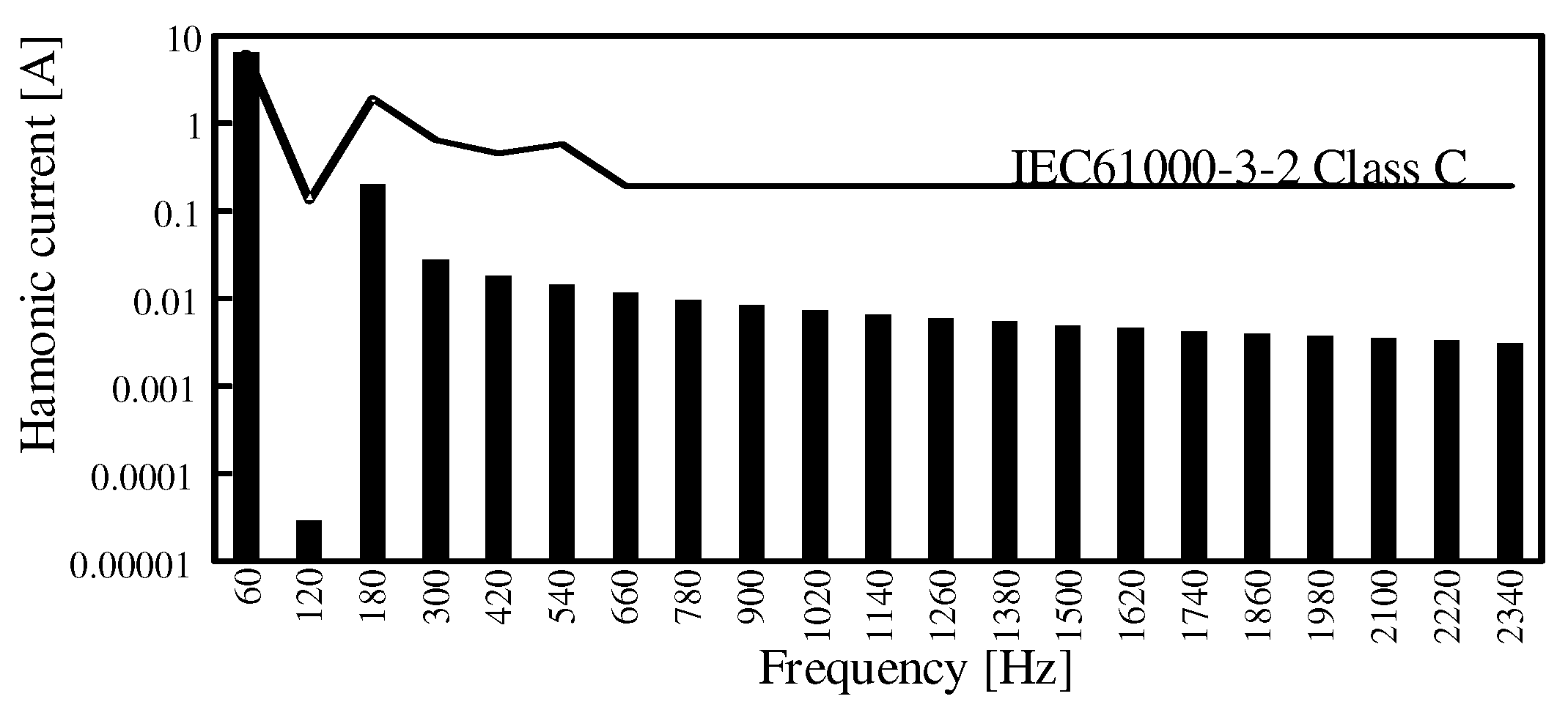
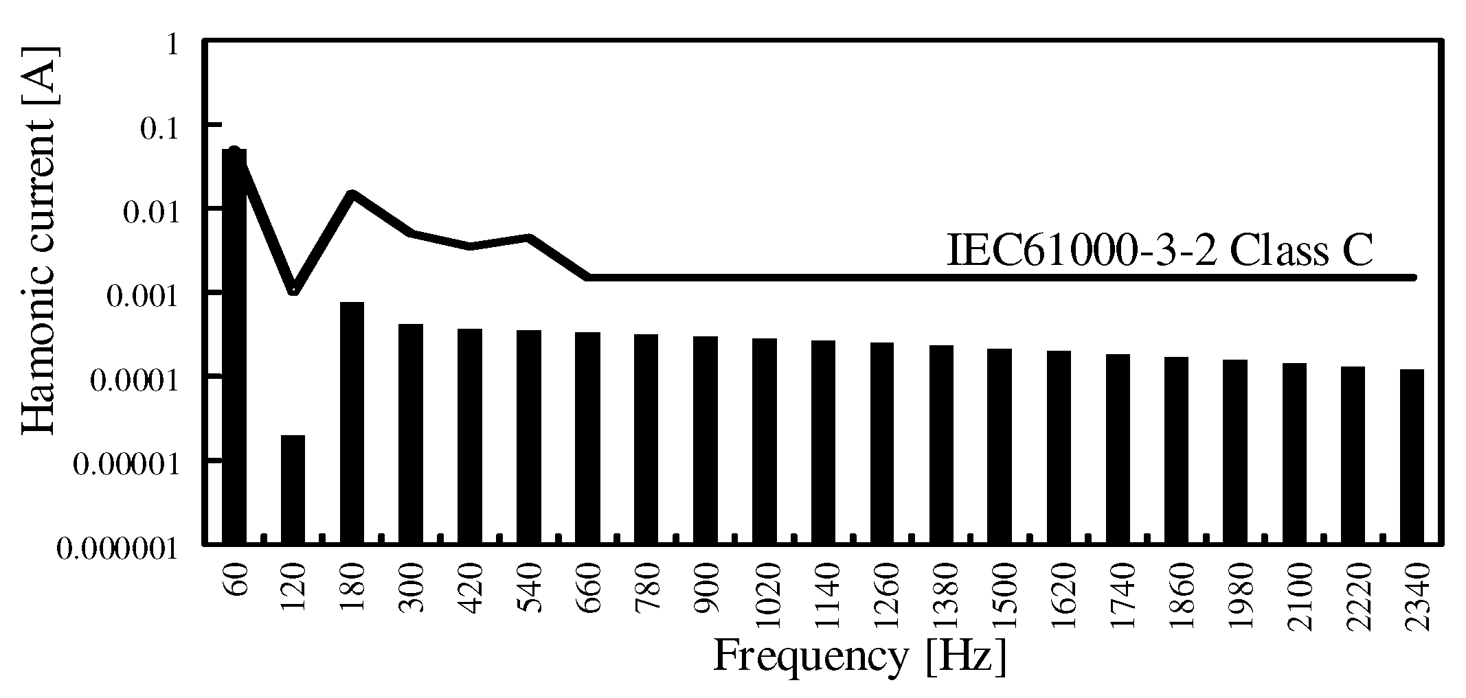
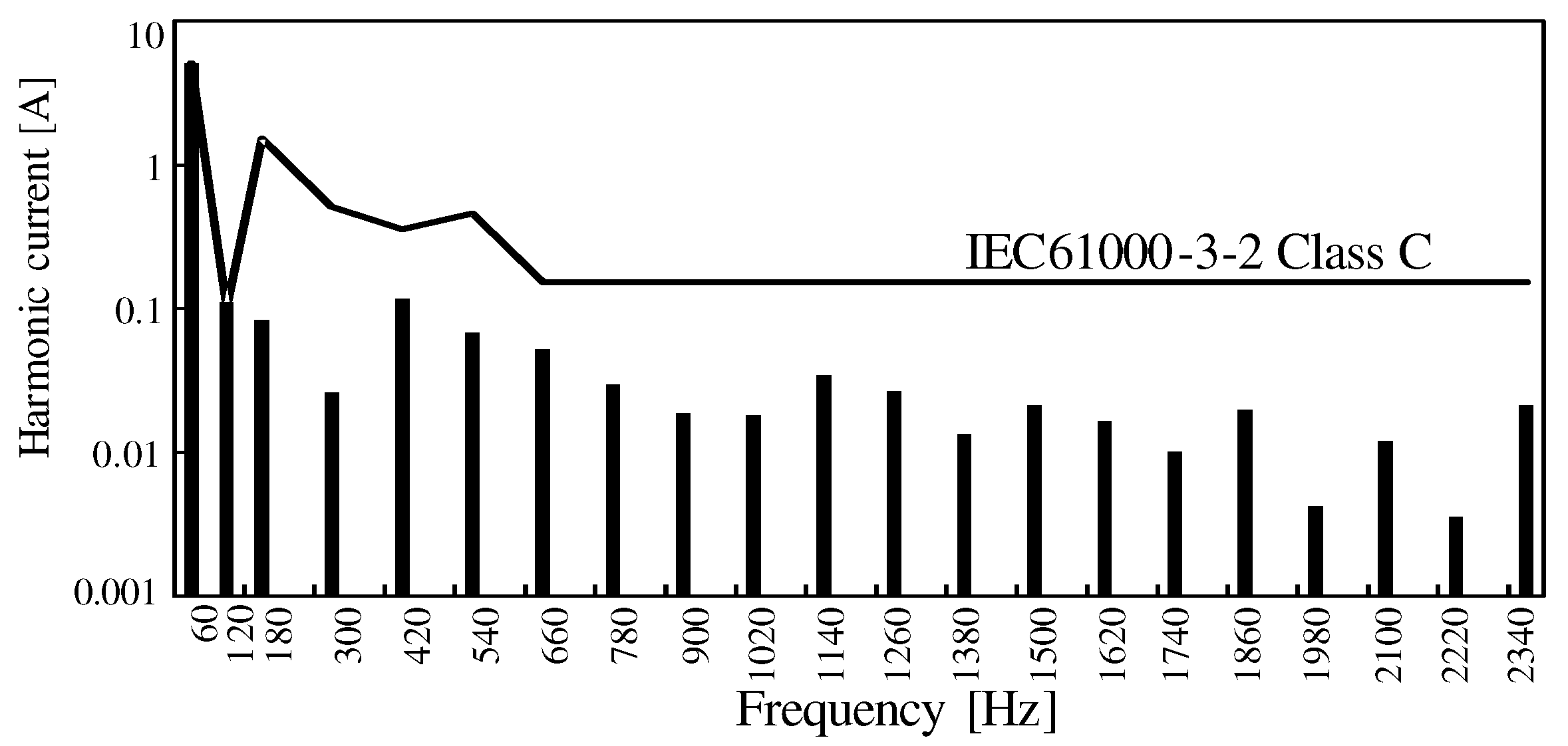
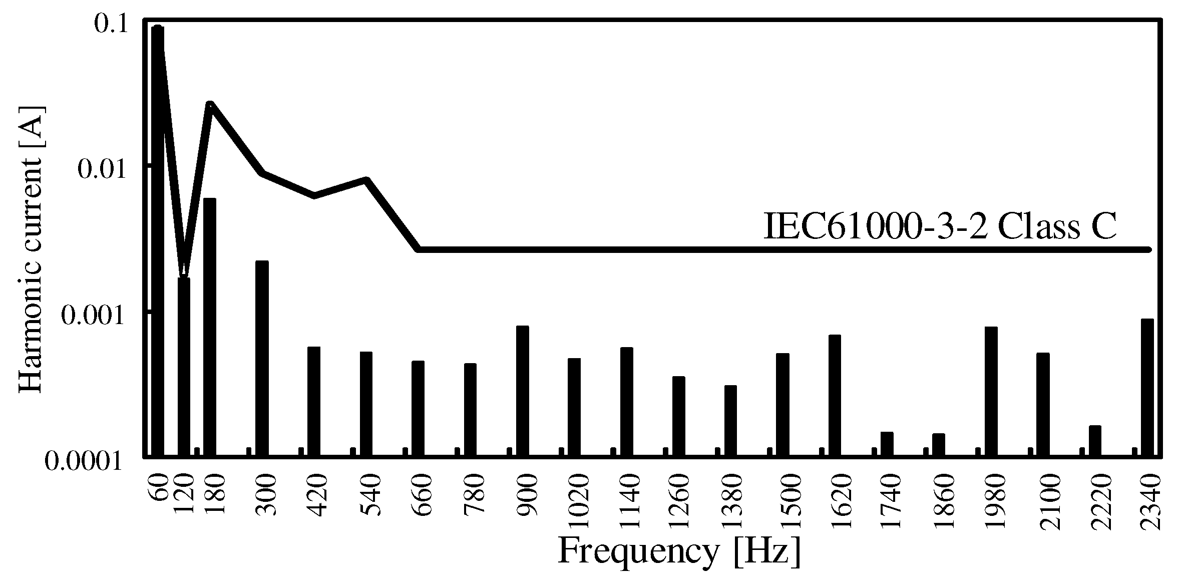
- Design of the smoothing capacitor for satisfying the standard of Electrical Applications and Materials Safety Act in Japan,
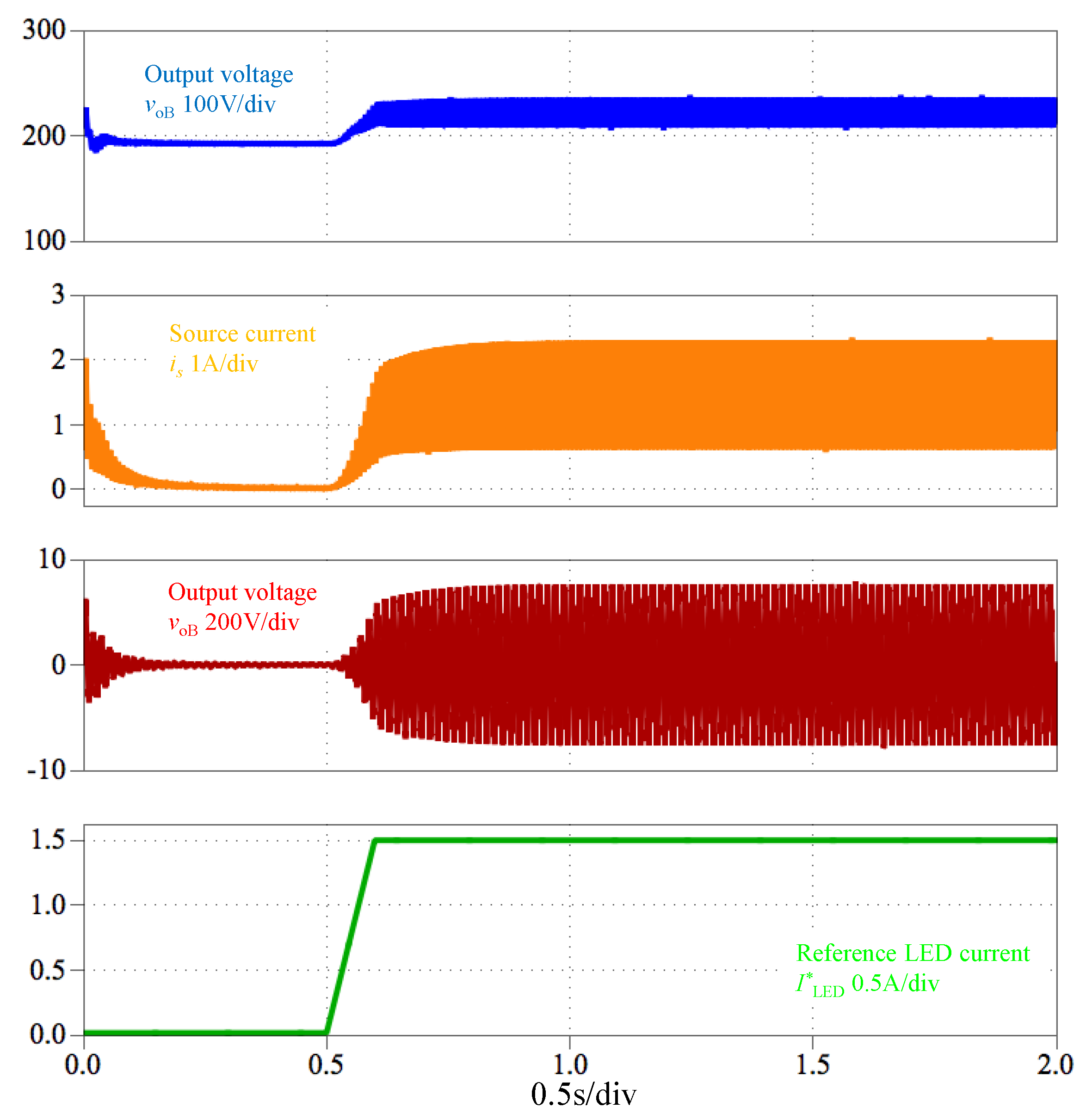
- Dynamic response of the proposed LED driver when the reference LED current is changed,
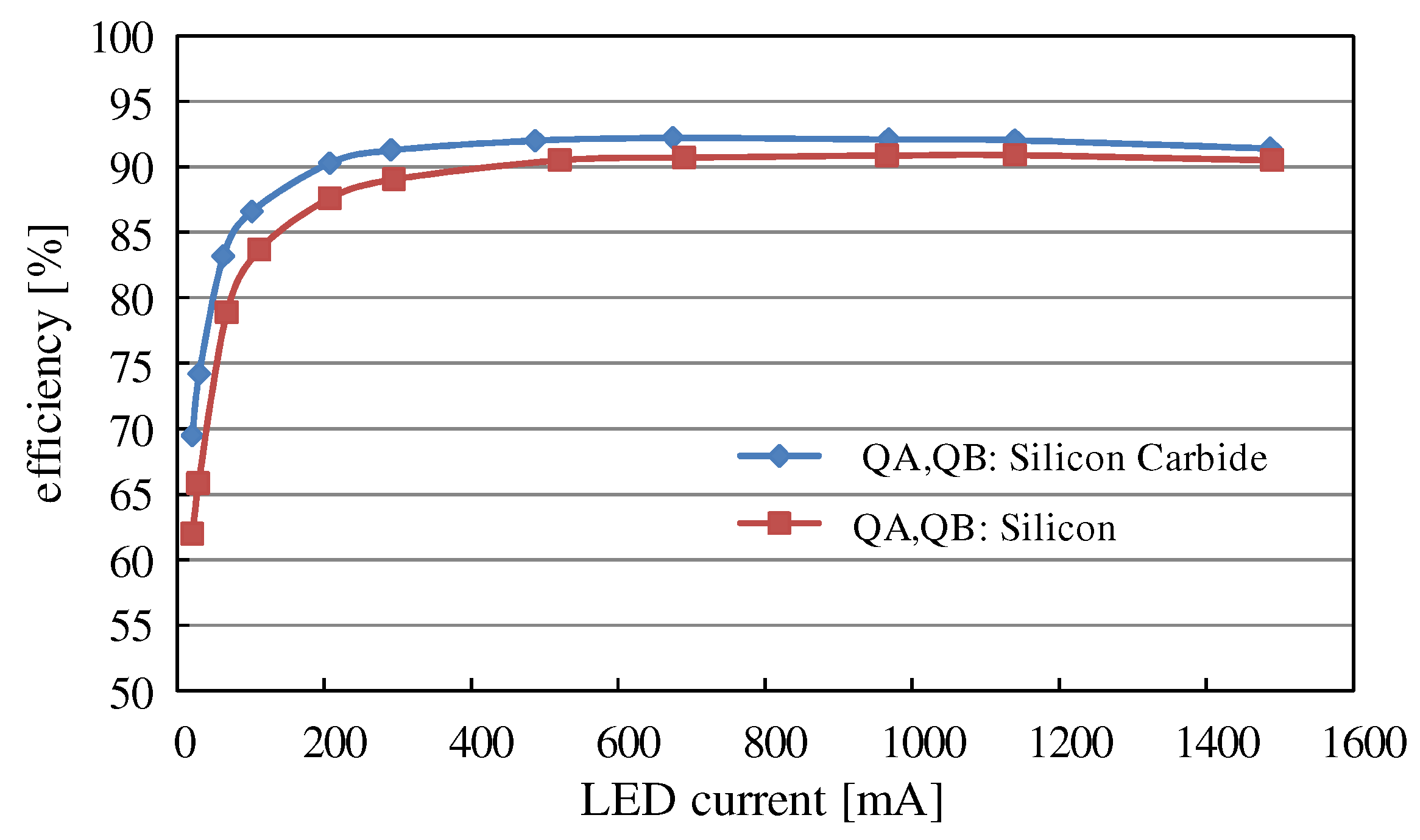
- Comparison of power conversion efficiency between Si- and SiC-MOSFETs,
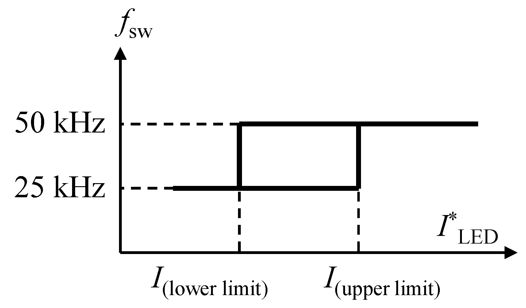
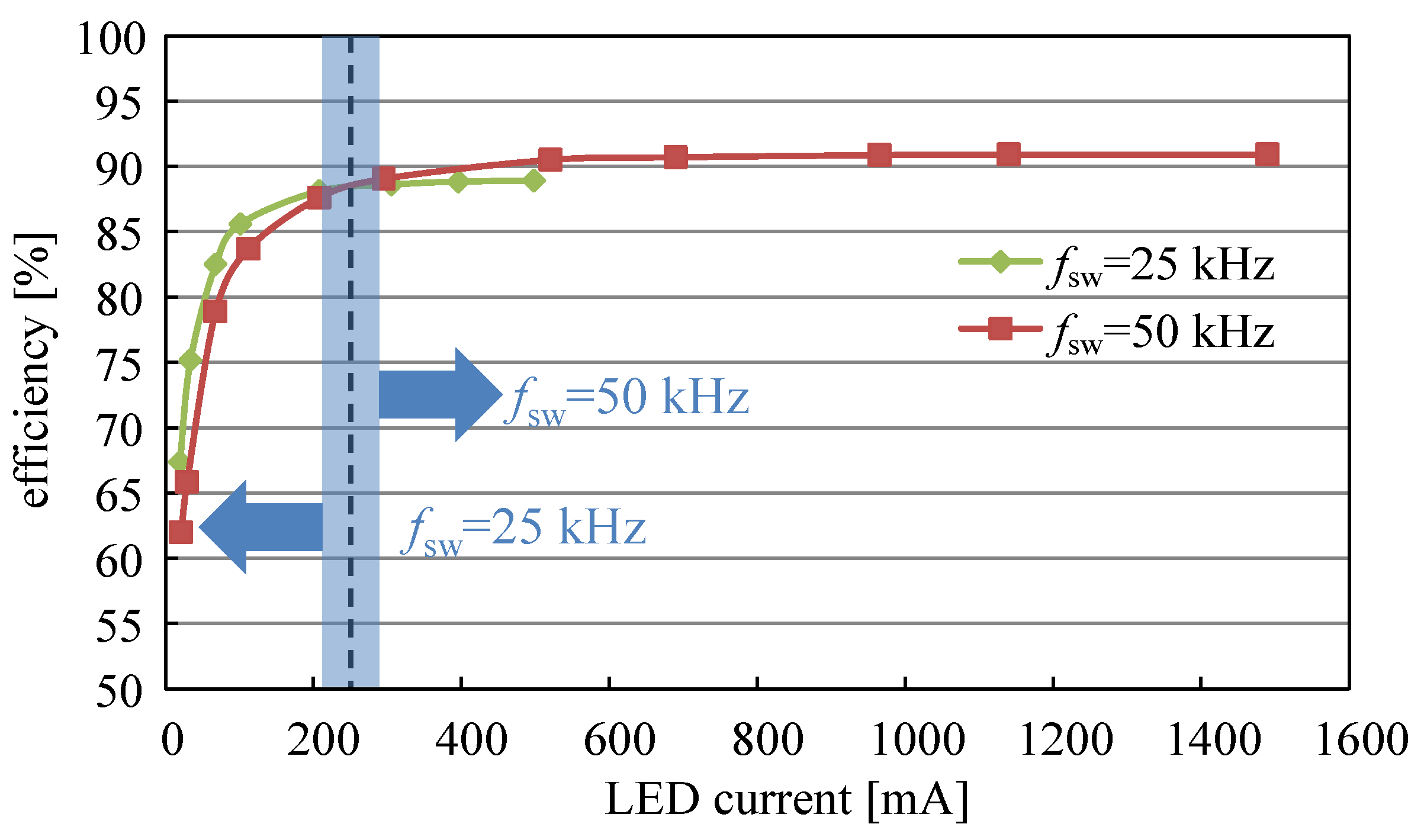
- Improvement of power conversion efficiency in low current range by the proposed variable switching frequency method.
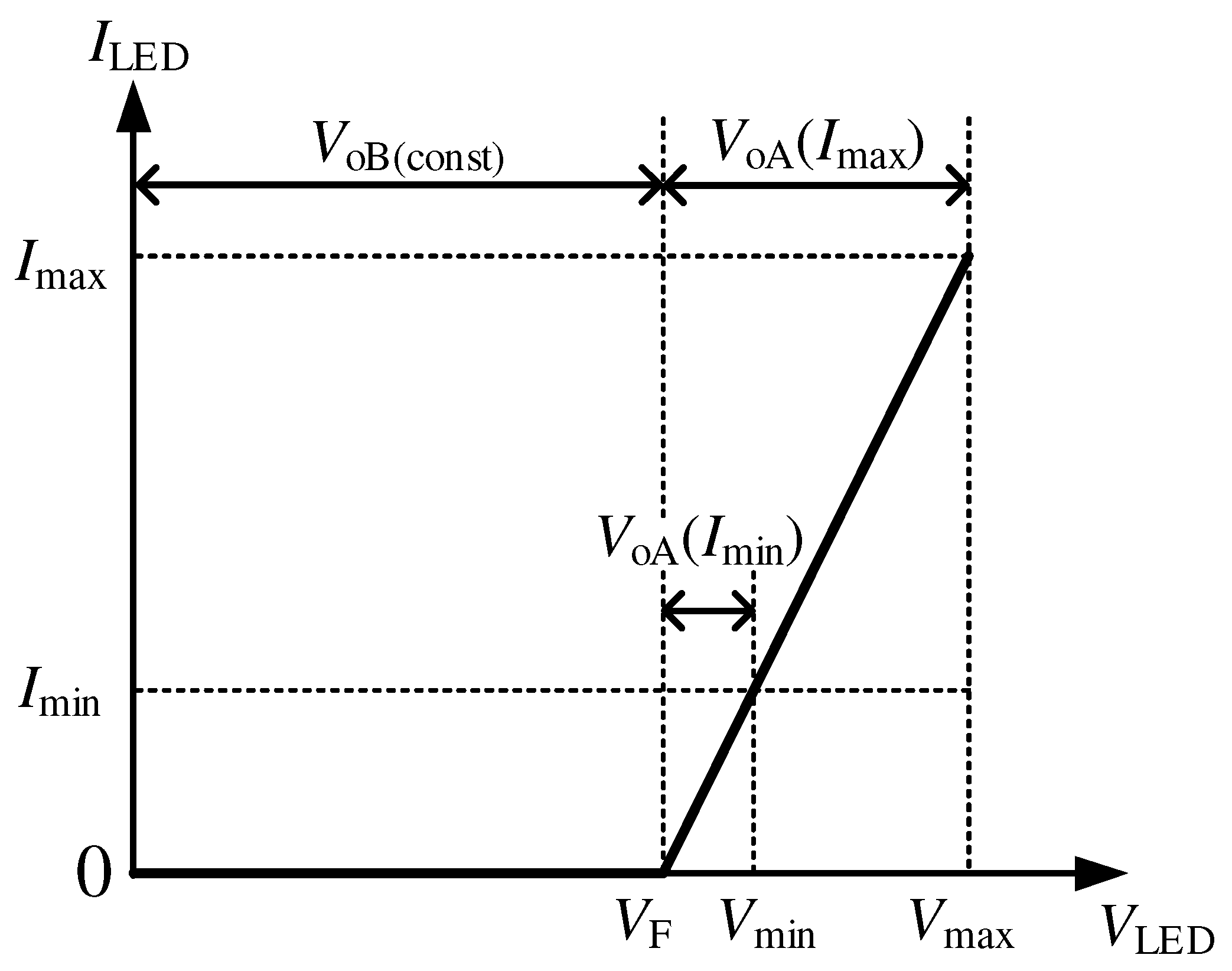
2. Conventional Control Method
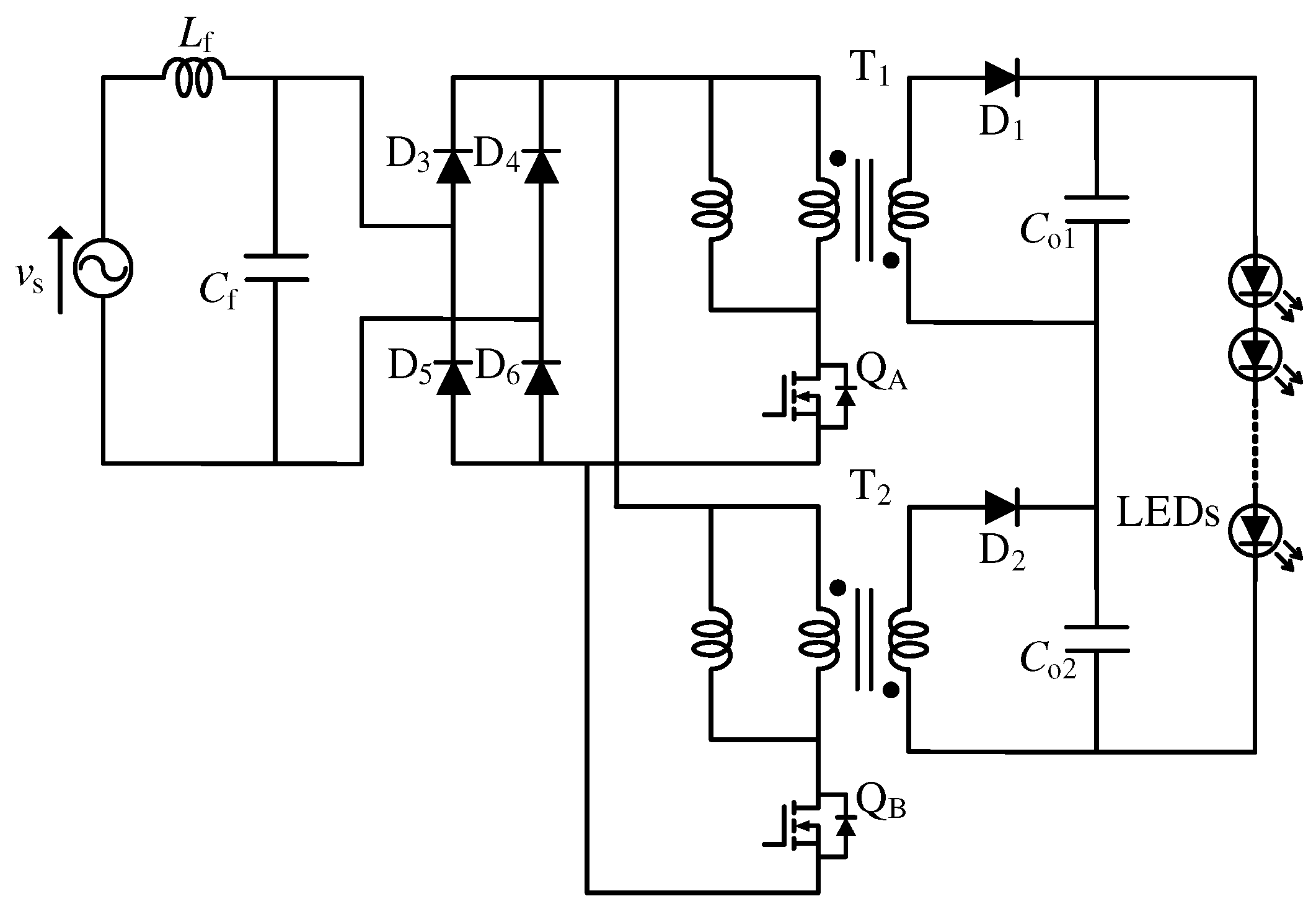
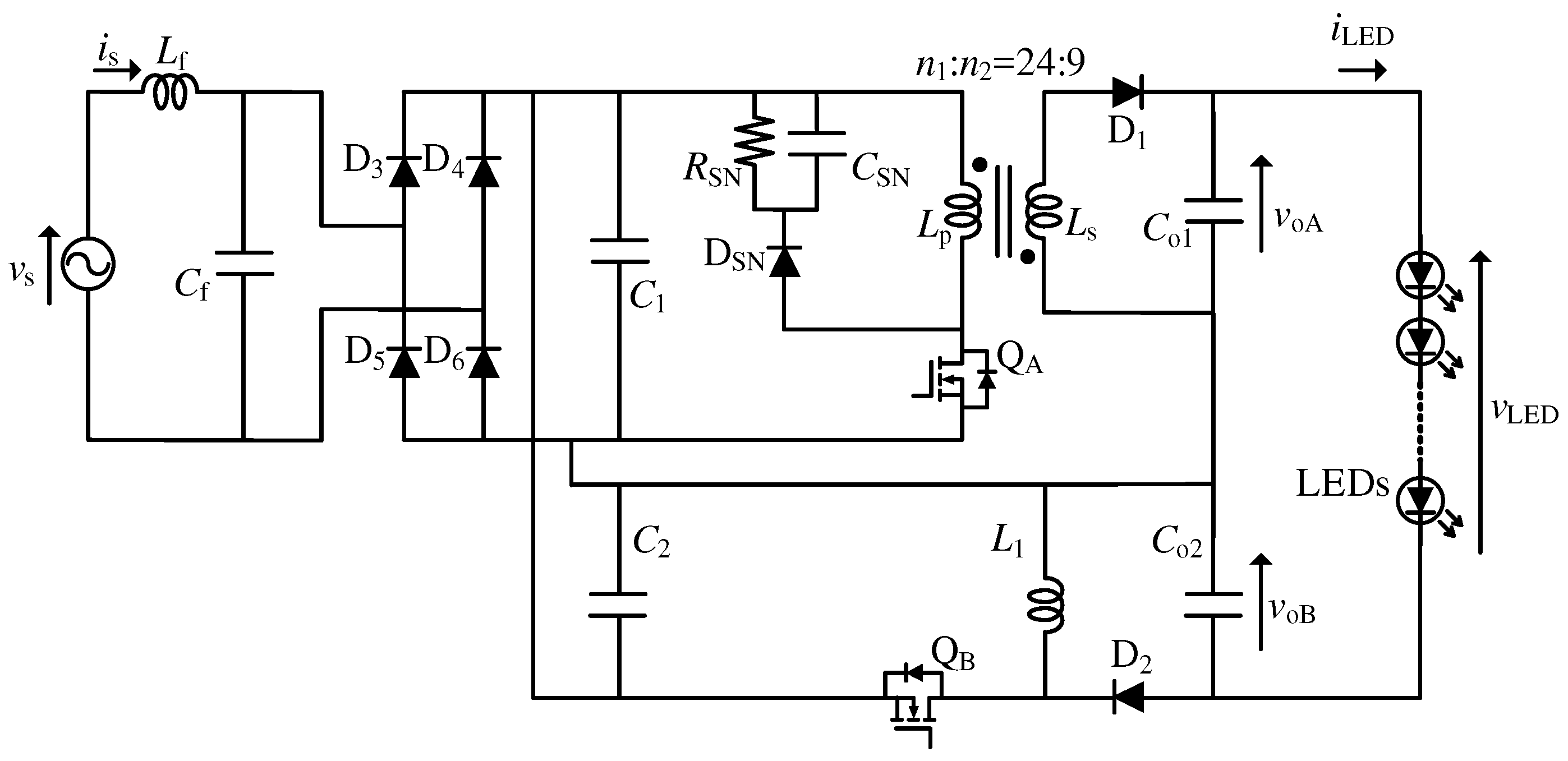
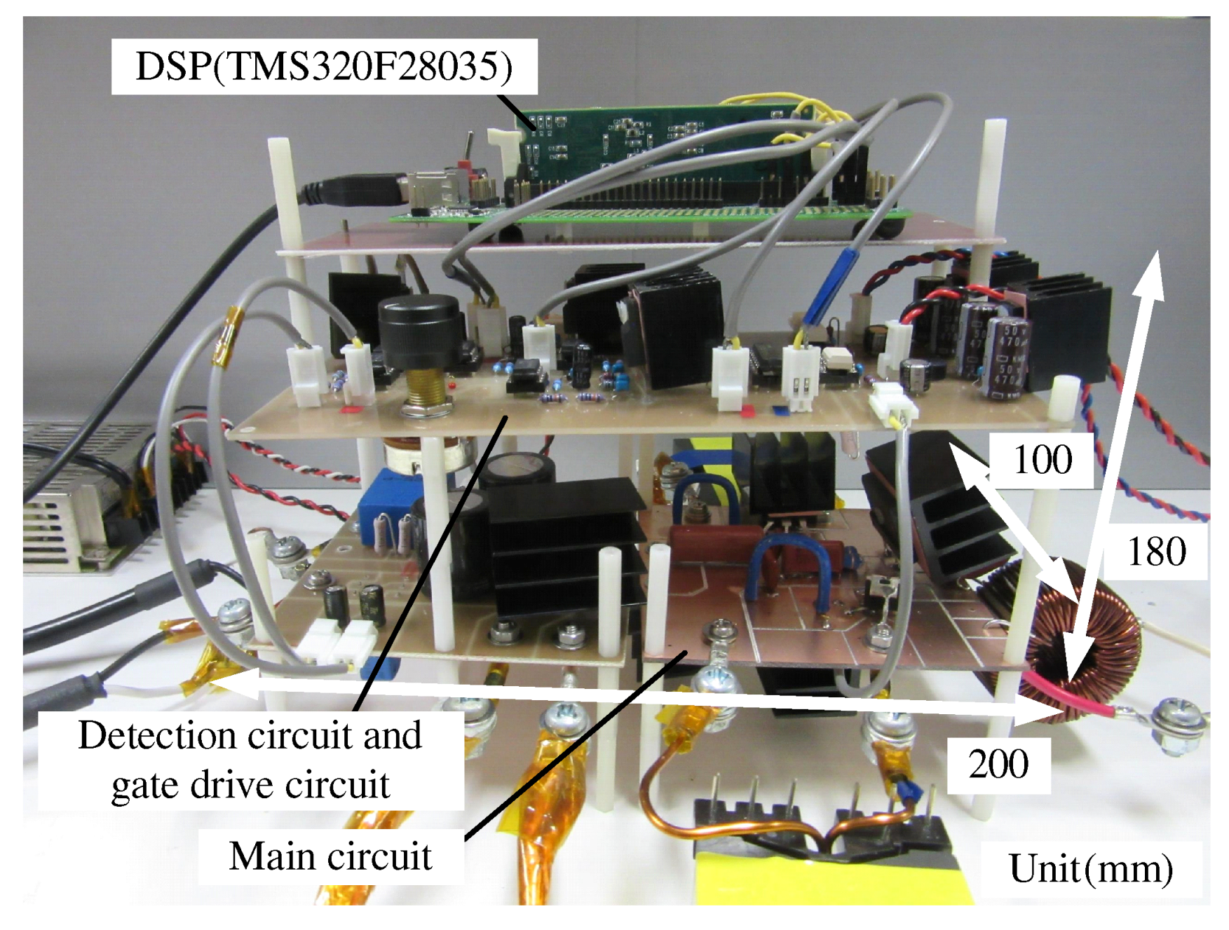
3. System Configuration
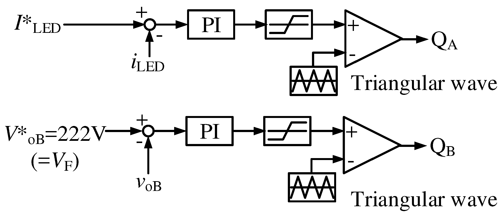
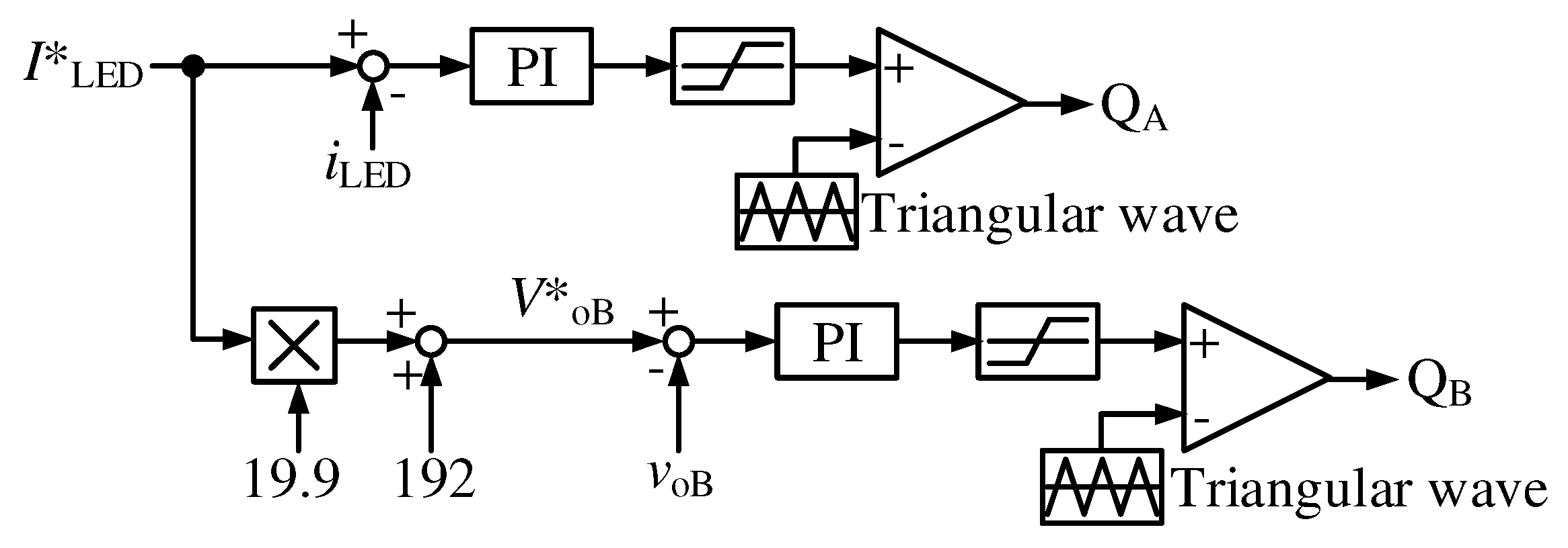
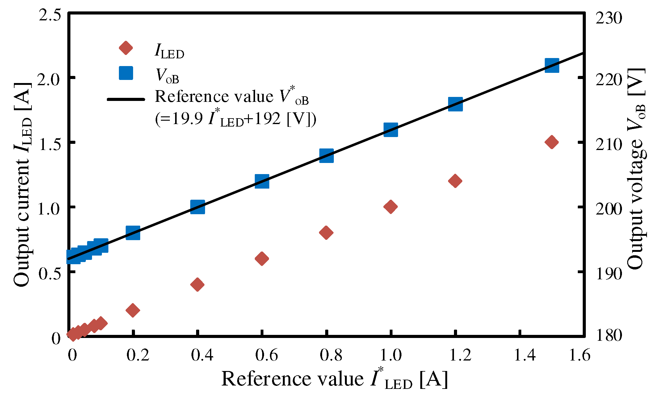
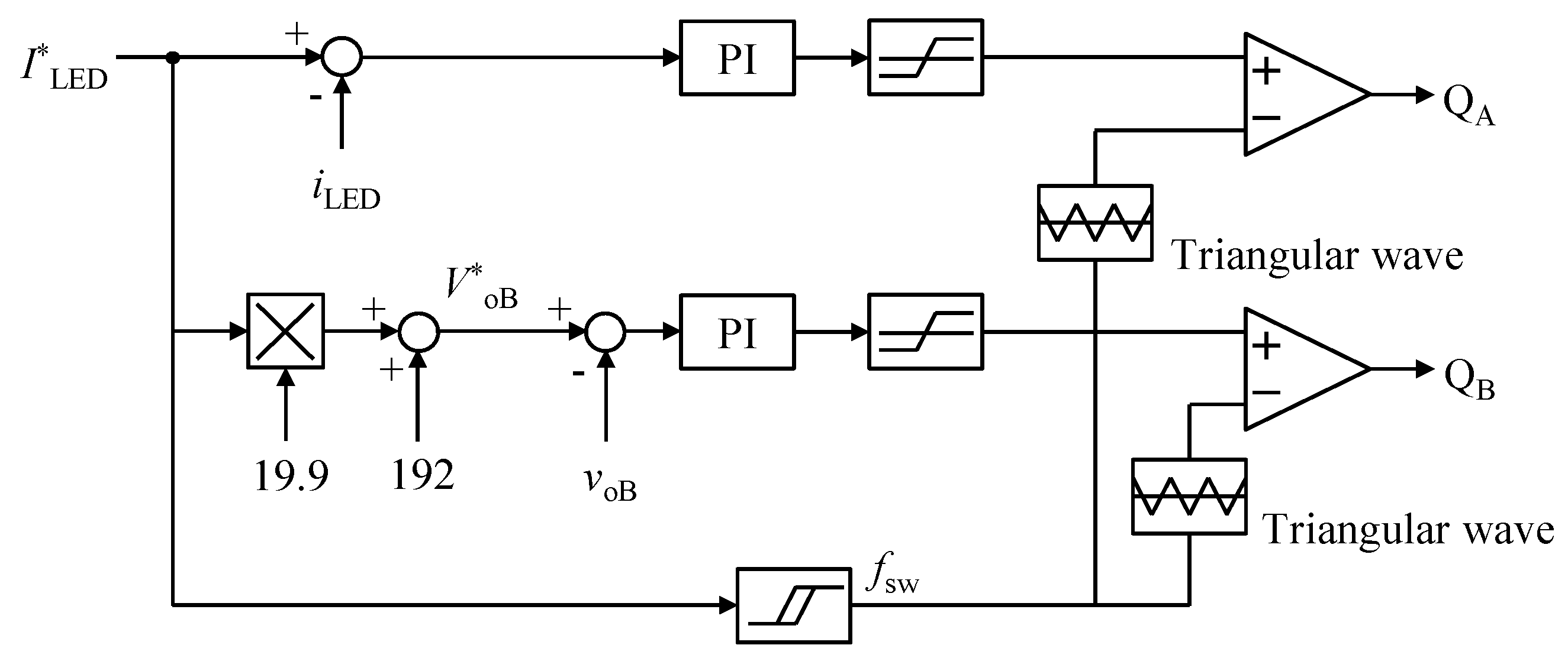
4. Proposed Cooperative Control Method
5. Simulation Results
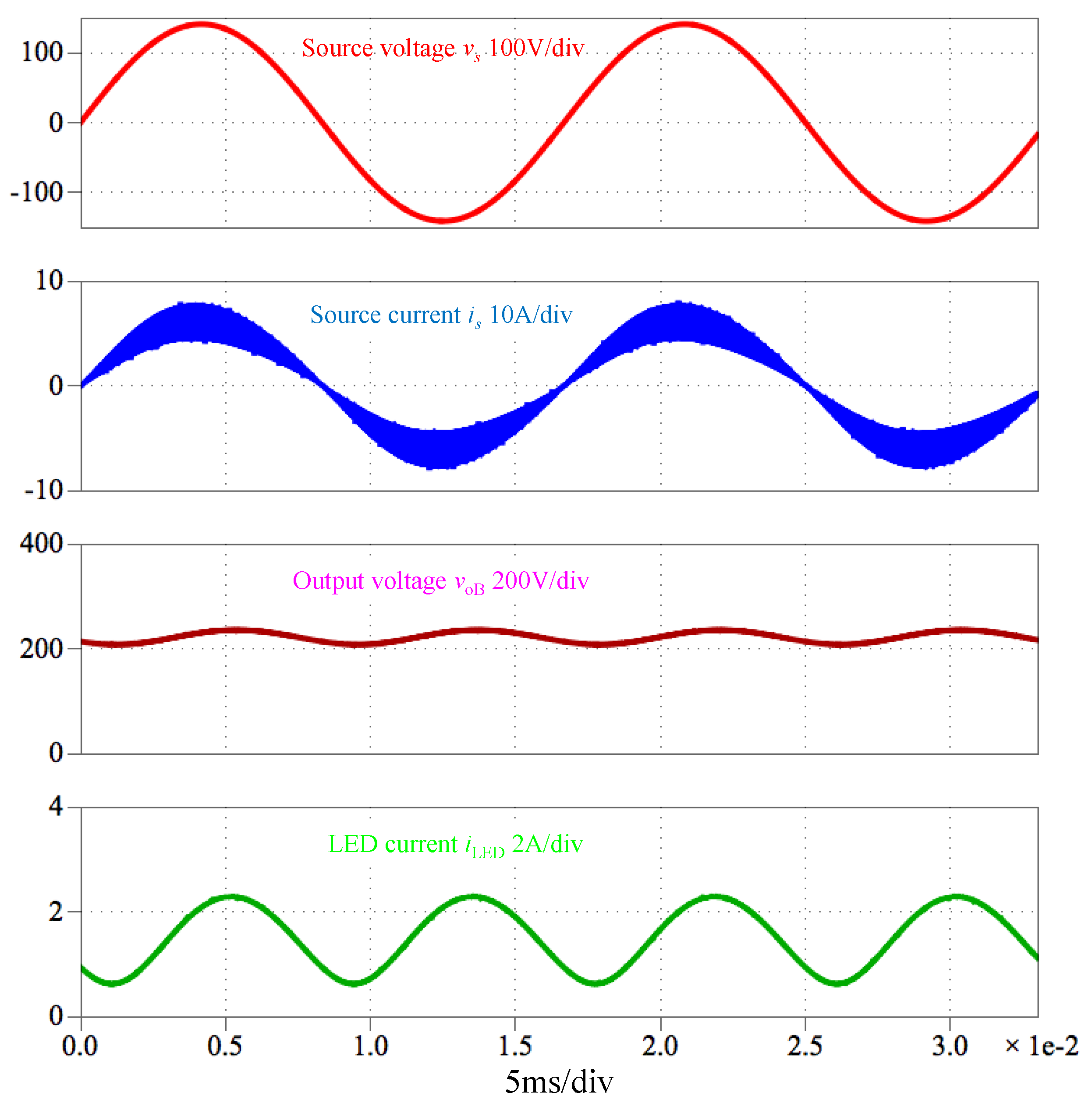
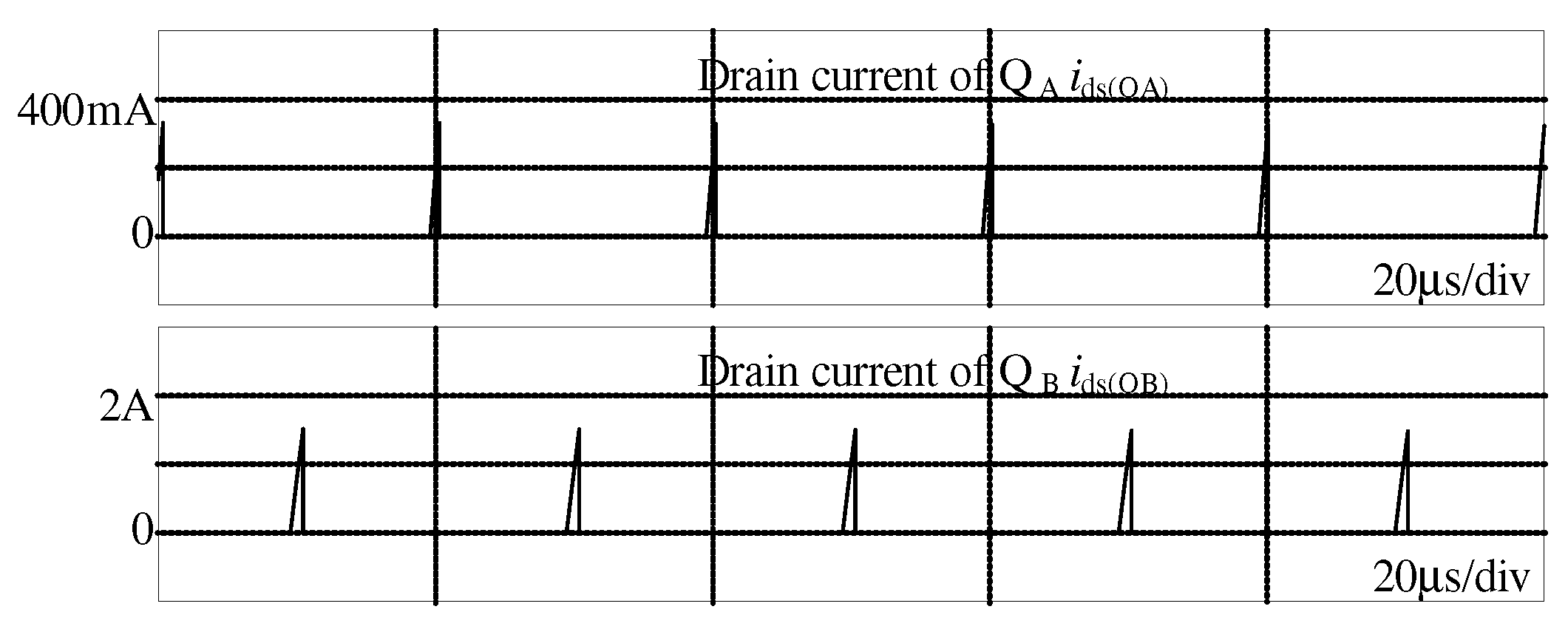
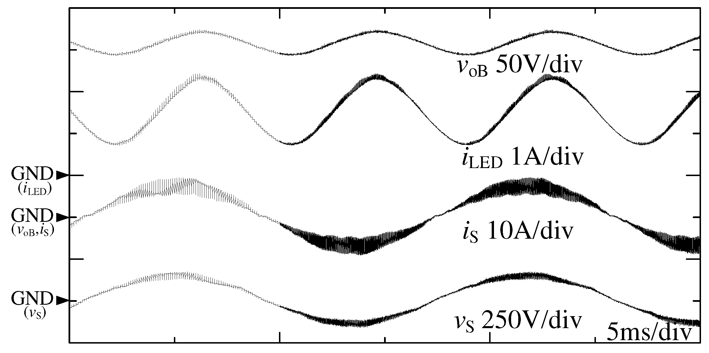
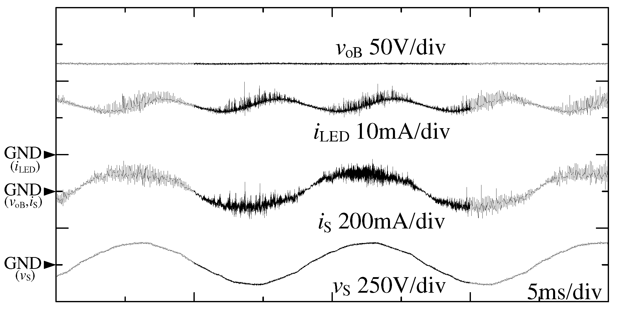
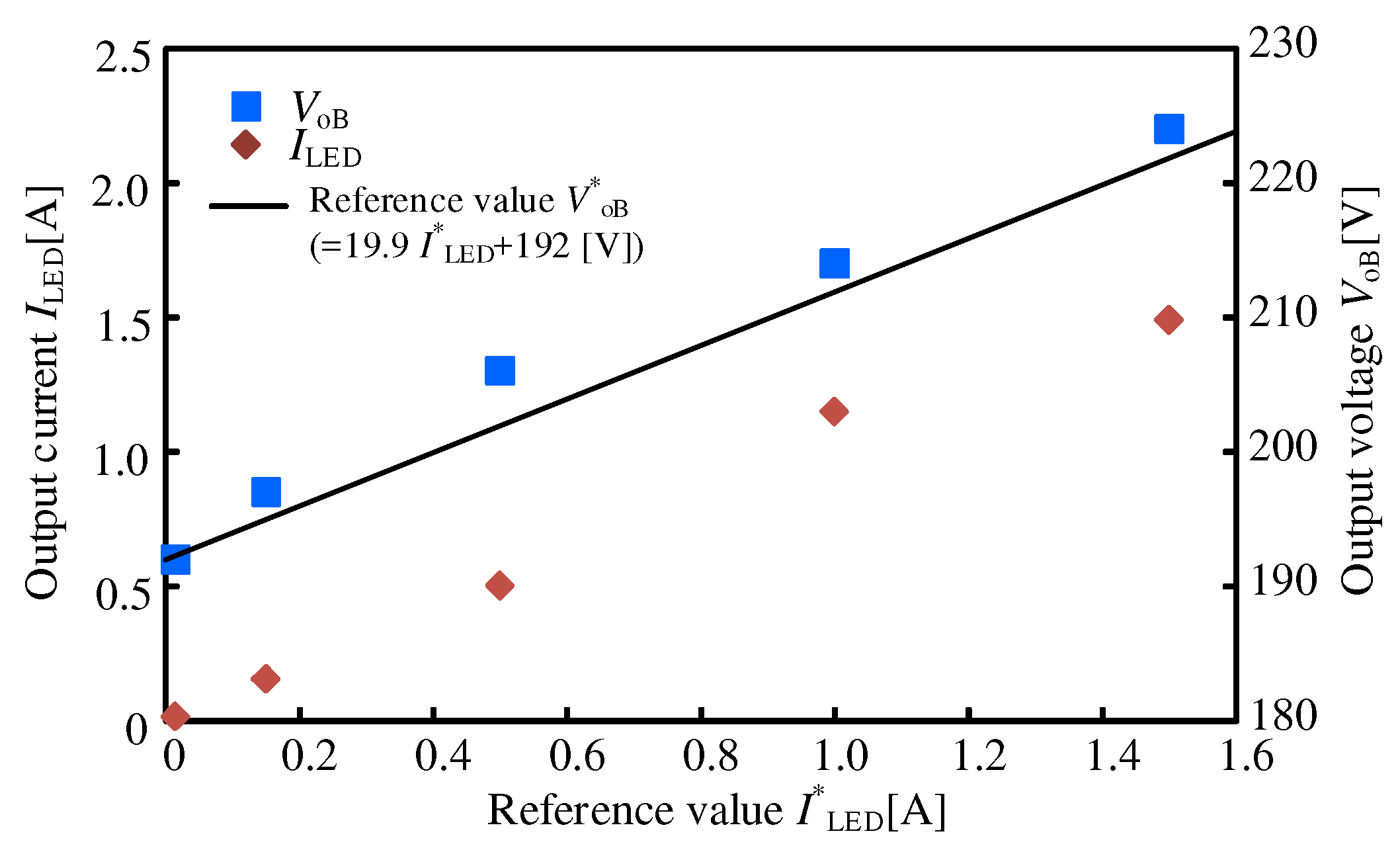
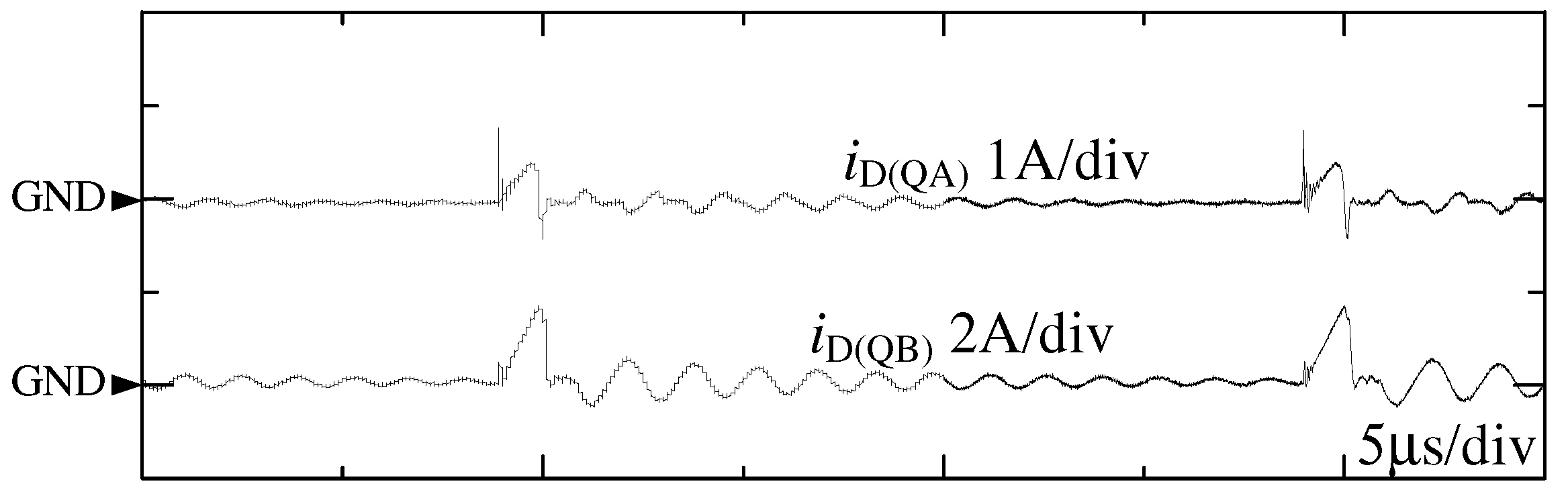
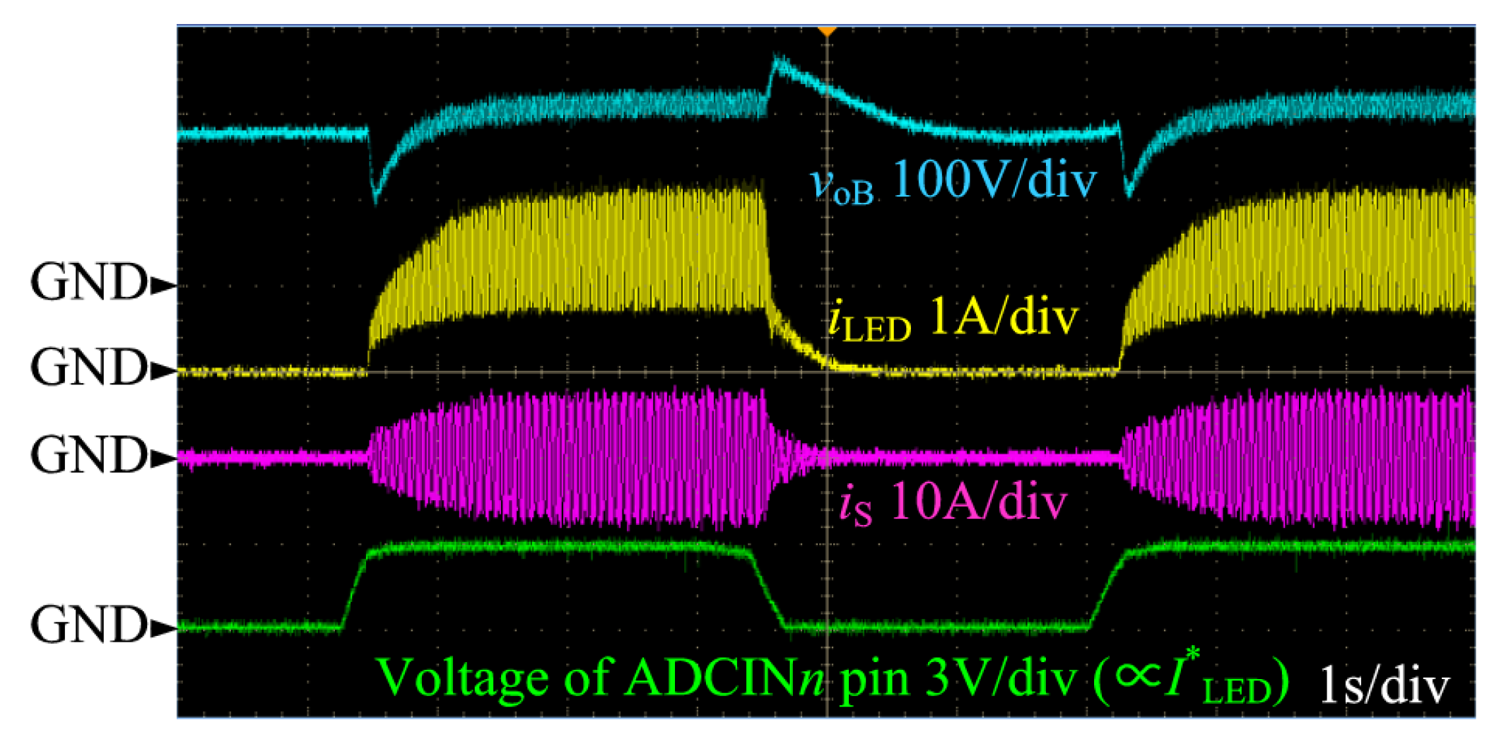
6. Experimental Results
7. Comparison of Power Conversion Efficiency between Si- and SiC-MOSFETs
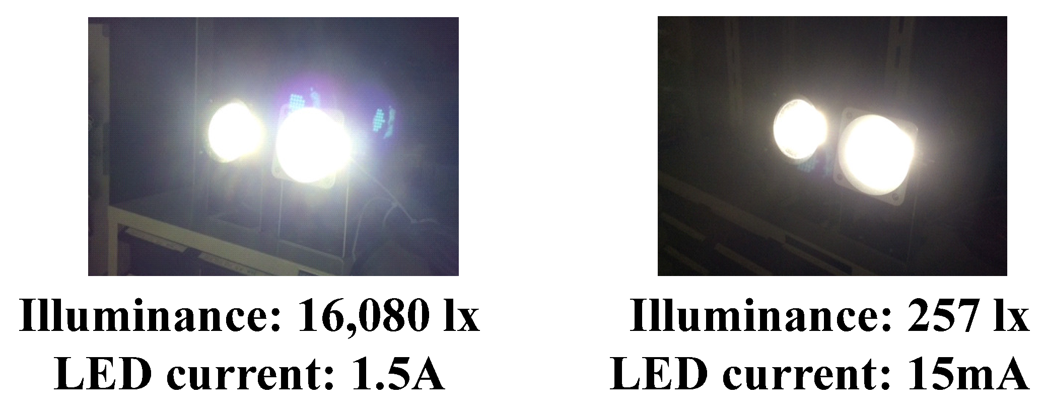
8. Improvement of Power Conversion Efficiency for Low LED Current Region
9. Conclusions
Author Contributions
Funding
Conflicts of Interest
Abbreviations
| LED | Light-emitting diode |
| DCM | Discontinuous conduction mode |
| THD | Total harmonic distortion |
| MOSFET | Metal-oxide-semiconductor field-effect transistor |
| PFC | Power factor correction |
| FFT | Fast Fourier Transform |
| DSP | Digital signal processor |
References
- International Energy Agency. Energy Matters. Available online: https://www.iea.org/publications/freepublications/publication/EnergyMattersBrochure.2.pdf (accessed on 25 July 2016).
- United Nations Environment. Minamata Convention on Mercury. Available online: http://www.unep.org/hazardoussubstances/Portals/9/Mercury/Documents/dipcon/CONF3Minamata%20Convention%20on%20Mercuryfinal%2026%2008e.pdf (accessed on 25 July 2016).
- Schratz, M.; Gupta, C.; Struhs, T.J.; Gray, K. Improving light quality with cost-effective LED technology. IEEE Ind. Appl. Mag. 2016, 22, 55–62. [Google Scholar] [CrossRef]
- Lee, J.-Y.; Moon, G.-W.; Park, H.-J.; Youn, M.-J. Integrated ZCS Quasi-Resonant Power Factor Correction Converter Based on Flyback Topology. IEEE Trans. Power Electron. 2000, 15, 634–643. [Google Scholar]
- Arias, M.; Lamar, D.G.; Linera, F.F.; Balocco, D.; Diallo, A.A.; Sebastian, J. Design of a Soft-Switching Asymmetrical Half-Bridge Converter as Second Stage of an LED Driver for Street Lighting Application. IEEE Trans. Power Electron. 2012, 27, 1608–1621. [Google Scholar] [CrossRef]
- Xie, X.; Li, J.; Peng, K.; Xhao, C.; Lu, Q. Study on the Single-Stage Forward-Flyback PFC Converter with QR Control. IEEE Trans. Power Electron. 2016, 31, 430–442. [Google Scholar] [CrossRef]
- Cheng, C.-A.; Cheng, H.-L.; Chung, T.-Y. A Novel Single-Stage High-Power-Factor LED Street-Lighting Driver With Coupled Inductors. IEEE Trans. Ind. Appl. 2014, 50, 3037–3045. [Google Scholar] [CrossRef]
- Cheng, C.-A.; Chang, C.-H.; Chung, T.-Y.; Yang, F.-L. Design and Implementation of a Single-Stage Driver for Supplying an LED Street-Lighting Module With Power Factor Corrections. IEEE Trans. Power Electron. 2015, 30, 956–966. [Google Scholar] [CrossRef]
- Moo, C.-S.; Chen, Y.-J.; Yang, W.-C. An Efficient Driver for Dimmable LED Lighting. IEEE Trans. Power Electron. 2012, 27, 4613–4618. [Google Scholar] [CrossRef]
- Jane, G.; Su, C.-C.; Chiu, H.-J.; Lo, Y.-K. High-Efficiency LED Driver for Street Light Applications. In Proceedings of the International Conference on Renewable Energy Research and Applications (ICRERA), Nagasaki, Japan, 11–14 November 2012; pp. 105–107. [Google Scholar]
- Yada, T.; Yamada, H.; Hanamoto, T. A Novel Cooperational Control Method for LED Driver with Parallel Flyback Converter. J. Jpn. Inst. Power Electron. 2015, 40, JIPE-40-19. [Google Scholar]
- Katamoto, Y.; Yamada, H.; Tanaka, T.; Okamoto, M.; Yada, T. Experimental Verification of Cooperative Control Method for 400-W Class LED Drivfer With Wide Dimming Range. In Proceedings of the 19th International Conference on Electrical Machines and Systems, Chiba, Japan, 13–16 November 2016; p. DS4G-2-8. [Google Scholar]
- Ministry of Economy, Trade, and Industry. Electrical Appliances and Materials Safety Act; Ministry of Economy, Trade and Industry: Chiyoda, Japan, 2018.


| Item | Symbol | Value |
|---|---|---|
| AC source voltage | 100 Vrms | |
| Inductance of filter inductor | 265 µH | |
| Capacitance of filter capasitor | 0.1 µF | |
| Capacitance | , | 0.1 µF, 0.1 µF |
| Capacitance | , | 110 µF, 110 µF |
| Buck-boost inductance | 69 µH | |
| Turn ratio | : | 24:9 |
| Inductance of primary side | 228 µH | |
| Snubber resistance | 23.5 k | |
| Snubber Capacitance | 1 nF | |
| Switching frequency | 50 kHz |
| Parameter | (SiC-MOSFET) | (Si-MOSFET) | (SiC-MOSFET) | (Si-MOSFET) | |
|---|---|---|---|---|---|
| C3M0065090J | STF20NM65N | C2M0040120D | TK40J60T | ||
| Drain-source voltage (V) | 900 | 650 | 1200 | 600 | |
| Gate-source voltage (V) | −8/19 | −25/25 | −10/25 | −30/30 | |
| Continuous drain current (A) | = 25 °C | 35 | 15 | 40 | 40 |
| = 100 °C | 22 | 9.45 | 60 | - | |
| Junction temperature (°C) | −55 to 150 | −55 to 150 | −55 to 150 | −55 to 150 | |
| Drain-source on-state resistance (m) | = 25 °C | 65 | 250 | 40 | 68 |
| = 100 °C | 78 | 270 | 52 | 80 | |
| Input capacitance (pF) | 660 | 1280 | 1893 | 3900 | |
| Output capacitance (pF) | 60 | 110 | 150 | 9200 | |
| Reverse capacitance (pF) | 4.0 | 10 | 10 | 280 | |
| Item | Conventional Method | Proposed Method | Proposed Method |
|---|---|---|---|
| with Si-MOSFETs | with SiC-MOSFETs | ||
| AC input voltage | 185–265 Vrms | 100 Vrms | 100 Vrms |
| Output power | 210 W | 408 W | 408 W |
| Dimming type | Step | Linear | Linear |
| Dimming range (%) | 50, 75, 100 | 1–100 | 1–100 |
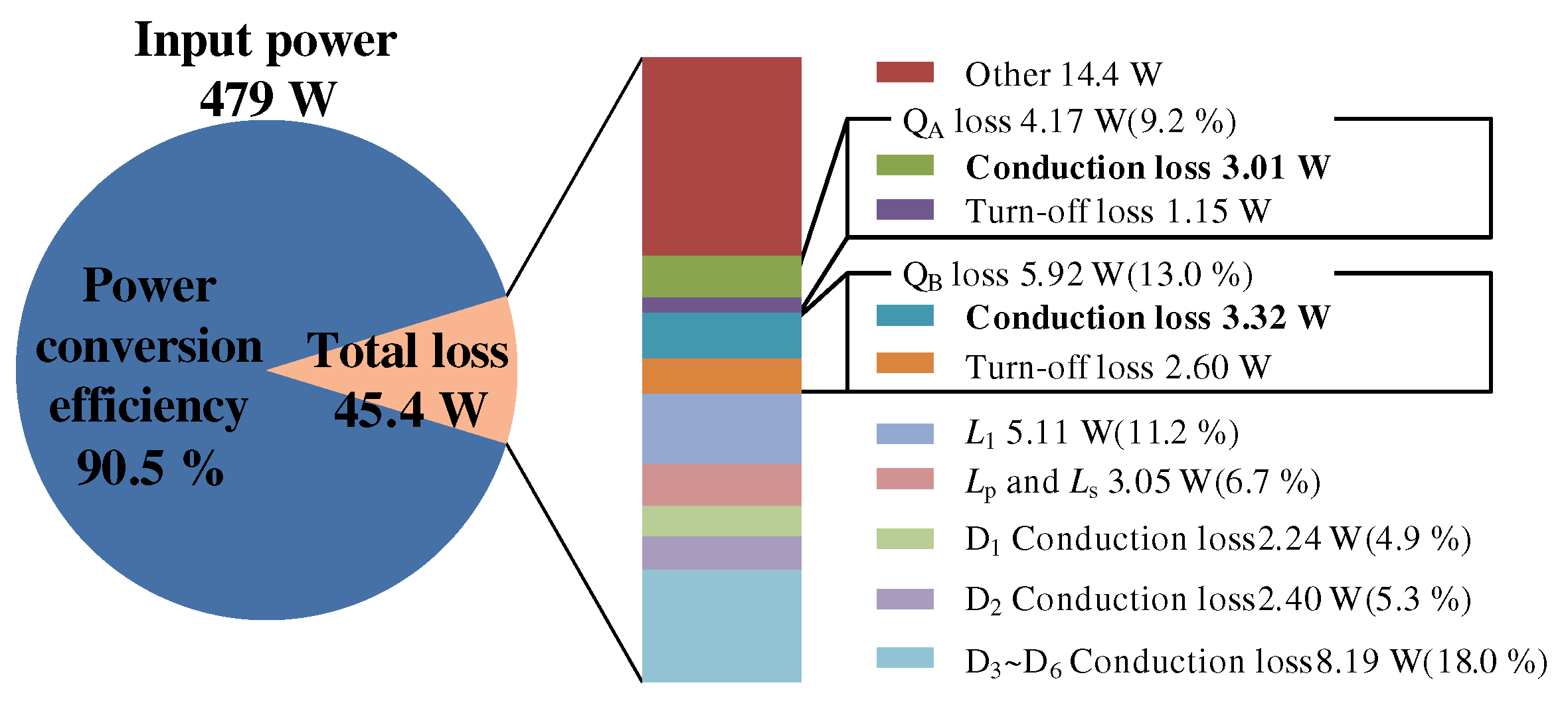
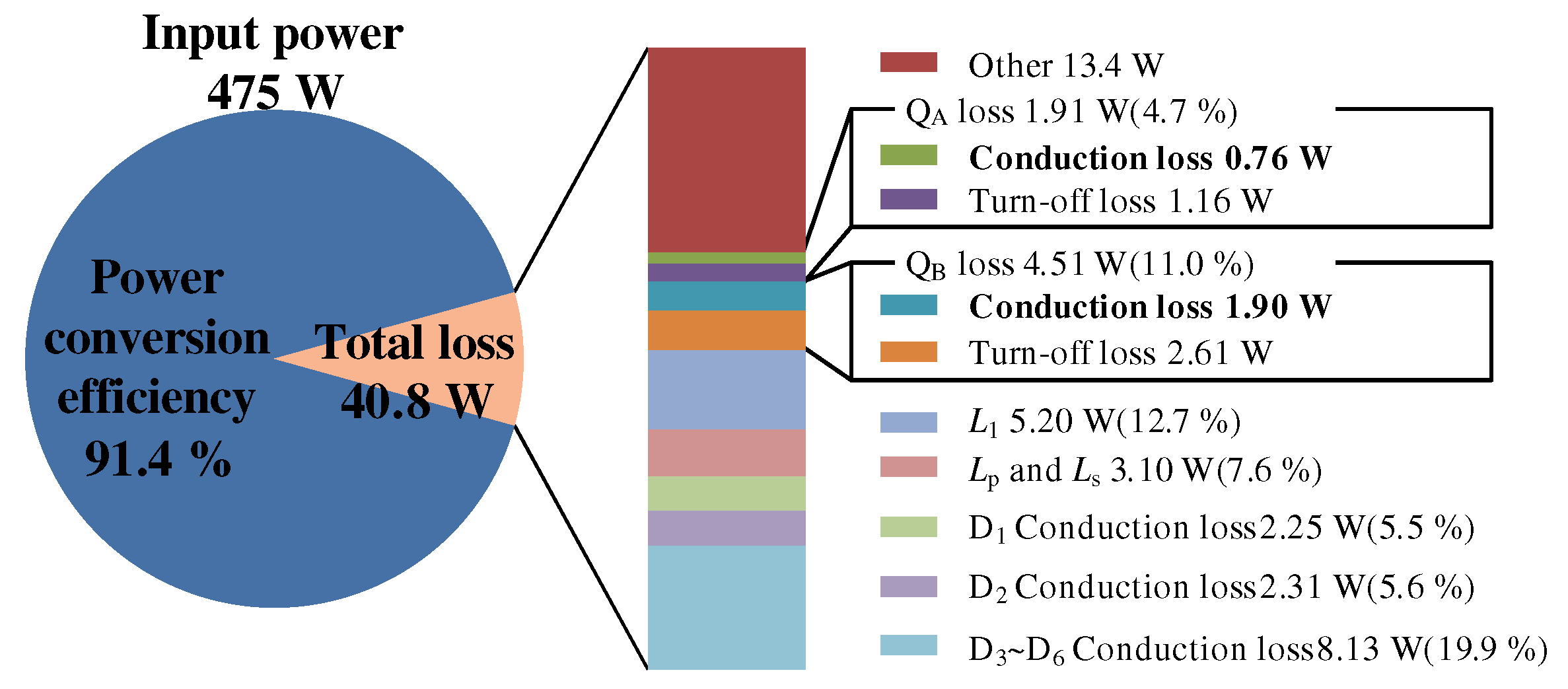
| Efficiency at maximum output power | 92.1% | 90.5% | 91.4% |
| Efficiency at minimum output power | 90.7% | 62.0% | 69.5% |
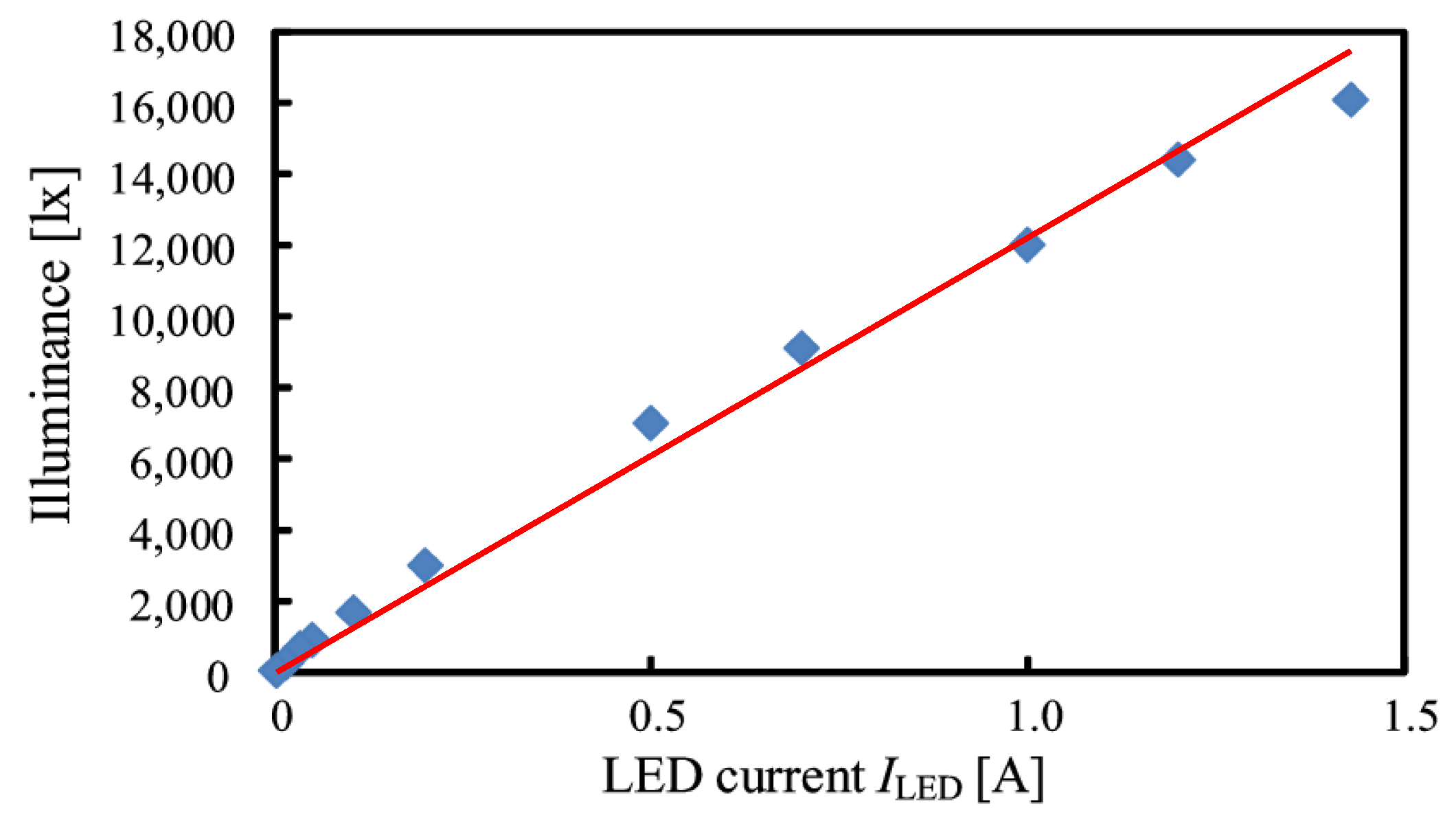
| Minimum illuminance of LEDs | 1680lx | 257lx | 257lx |
| Item | Si-MOSFET | SiC-MOSFET | Si-MOSFET | SiC-MOSFET |
| Loss | 4.17 W | 1.91 W | 5.92 W | 4.51 W |
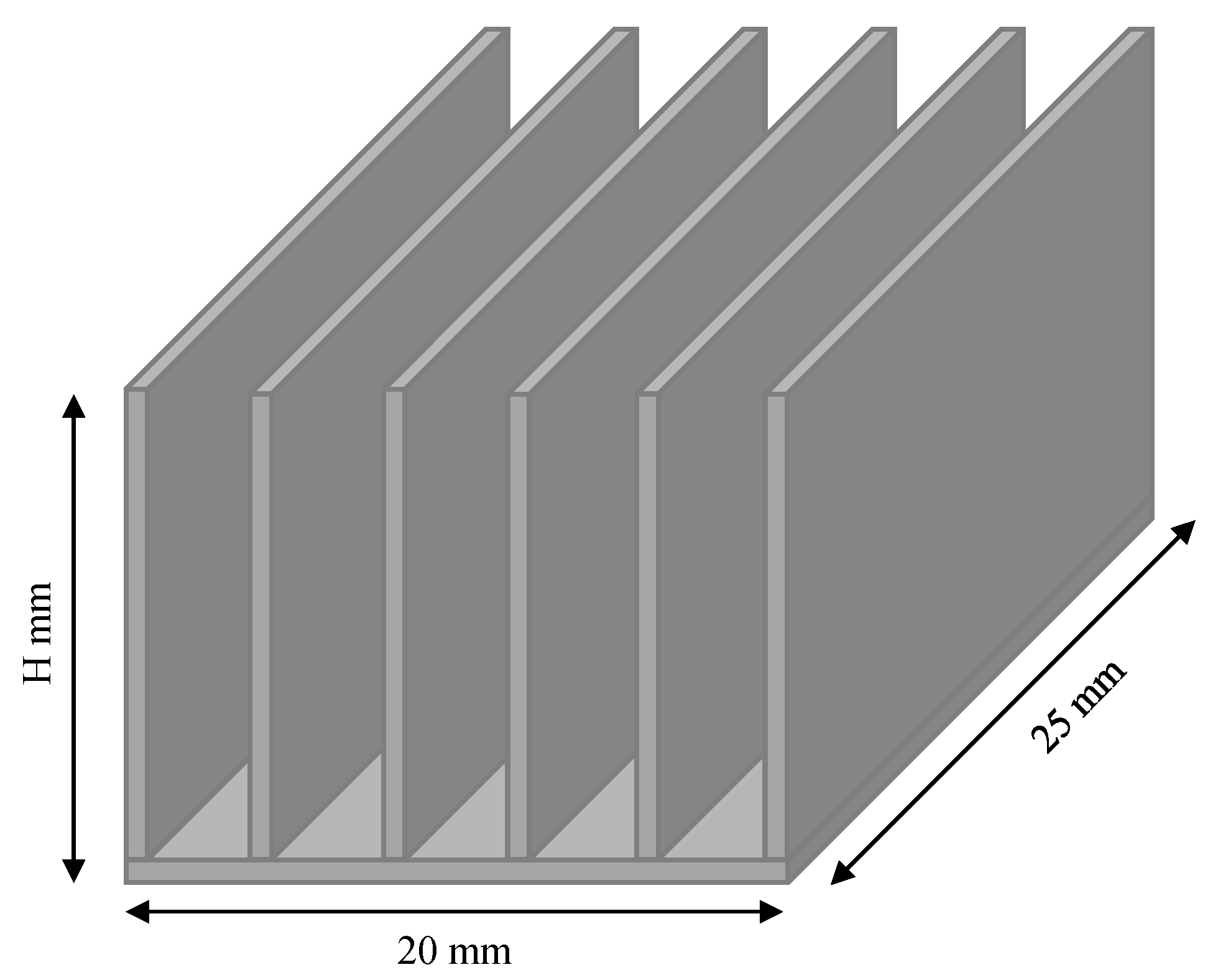
| Height of the heat sink | 37 mm | 14.4 mm | 61.2 mm | 41.2 mm |
© 2018 by the authors. Licensee MDPI, Basel, Switzerland. This article is an open access article distributed under the terms and conditions of the Creative Commons Attribution (CC BY) license (http://creativecommons.org/licenses/by/4.0/).
Share and Cite
Yada, T.; Katamoto, Y.; Yamada, H.; Tanaka, T.; Okamoto, M.; Hanamoto, T. Design and Experimental Verification of 400-W Class LED Driver with Cooperative Control Method for Two-Parallel Connected DC/DC Converters. Energies 2018, 11, 2237. https://doi.org/10.3390/en11092237
Yada T, Katamoto Y, Yamada H, Tanaka T, Okamoto M, Hanamoto T. Design and Experimental Verification of 400-W Class LED Driver with Cooperative Control Method for Two-Parallel Connected DC/DC Converters. Energies. 2018; 11(9):2237. https://doi.org/10.3390/en11092237
Chicago/Turabian StyleYada, Tomoharu, Yuta Katamoto, Hiroaki Yamada, Toshihiko Tanaka, Masayuki Okamoto, and Tsuyoshi Hanamoto. 2018. "Design and Experimental Verification of 400-W Class LED Driver with Cooperative Control Method for Two-Parallel Connected DC/DC Converters" Energies 11, no. 9: 2237. https://doi.org/10.3390/en11092237
APA StyleYada, T., Katamoto, Y., Yamada, H., Tanaka, T., Okamoto, M., & Hanamoto, T. (2018). Design and Experimental Verification of 400-W Class LED Driver with Cooperative Control Method for Two-Parallel Connected DC/DC Converters. Energies, 11(9), 2237. https://doi.org/10.3390/en11092237