Article

Multi-Objective Optimization Control for the Aerospace Dual-Active Bridge Power Converter

1
Key Laboratory of Aircraft Electric Propulsion Technology, Ministry of Industry and Information Technology of China, Northwestern Polytechnic University, Xi’an 710072, China
2
Shenyang Aircraft Design and Research Institute, Shenyang 110034, China
*
Author to whom correspondence should be addressed.
Energies 2018, 11(5), 1168; https://doi.org/10.3390/en11051168
Submission received: 27 March 2018 / Revised: 24 April 2018 / Accepted: 25 April 2018 / Published: 7 May 2018
(This article belongs to the Section F: Electrical Engineering)

Abstract

:
With the development of More Electrical Aircraft (MEA), the electrification of secondary power systems in aircraft is becoming more and more common. As the key power conversion device, the dual active bridge (DAB) converter is the power interface for the energy storage system with the high voltage direct current (HVDC) bus in aircraft electrical power systems. In this paper, a DAB DC-DC converter is designed to meet aviation requirements. The extended dual phase shifted control strategy is adopted, and a multi-objective genetic algorithm is applied to optimize its operating performance. Considering the three indicators of inductance current root mean square root (RMS) value, negative reverse power and direct current (DC) bias component of the current for the high frequency transformer as the optimization objectives, the DAB converter’s optimization model is derived to achieve soft switching as the main constraint condition. Optimized methods of controlling quantity for the DAB based on the evolution and genetic algorithm is used to solve the model, and a number of optimal control parameters are obtained under different load conditions. The results of digital, hard-in-loop simulation and hardware prototype experiments show that the three performance indexes are all suppressed greatly, and the optimization method proposed in this paper is reasonable. The work of this paper provides a theoretical basis and researching method for the multi-objective optimization of the power converter in the aircraft electrical power system.

1. Introduction

The aerospace industry is promoting the use of more electrical technology to enhance the performance and increase the reliability of aircraft power systems and secondary power subsystems instead of hydraulic, pneumatic systems. High voltage DC systems (HVDCs) are very popular in aircraft electric power systems because of their simpler equipment and significant energy savings. This technology requires high power density, reliable DC-DC converter for the application of battery storage power supplies to mission critical aerospace situations, e.g., actuators and avionics. DAB converters, as the interface of energy storage devices, have become a research hotspot [1,2]. The DAB converter has been popular among researchers over the last ten years due to its high performance, high efficiency, galvanic isolation and soft-switching property [3,4]. A DAB converter’s topology is shown in 
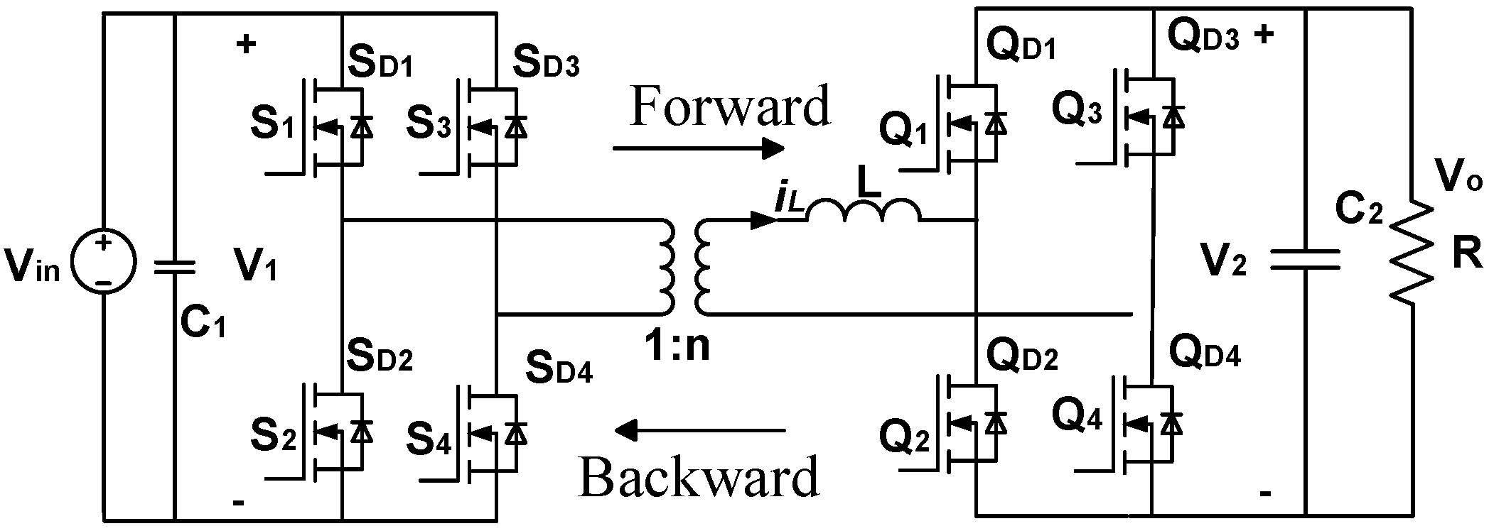
Figure 1. Because of the extra power switching devices, the pressure and flow capacity of the power switching are strong, so a larger power can be transmitted [5], but there are also some shortcomings [6], such as the increase of the inductance current value will increase the switching loss and switching stress make the switching device become damaged easily. In addition, there is a negative power transmission in the DAB converter, the circulation loss is large, so the transmission power peak in the circuit is increased, and the weight and volume of the transformer will be increased, which is not acceptable in aerospace context. The saturation of high frequency transformers will be caused by the DC bias component existing in the inductance current under the load transient variation, therefore, it how to optimize the dual active bridge DC-DC converter in aircraft electrical power systems has important practical significance.
At present, there are four main DAB converter topologies: single-phase/three-phase voltage source, single-phase current source, and single-phase resonant type. Control methods mainly focus on the phase shift control strategy, including single phase shift, double phase shift, expansion double phase shift, triple phase shift, phase shift plus pulse width modulation (PWM) hybrid control strategy, and model predictive control methods [7,8,9,10,11,12,13]. The single phase shift control strategy is simple and easy to realize, but the range of output power is narrow and reverse power exists. Multiple phase-shifting control methods have increased control variables, and the combination selection and calculation of multivariable is the key points to controlling the performance of DAB converters.
So far, many efforts have been made to improve the performance of DAB converters. Nevertheless, design considerations for high frequency DAB converter transformers are primarily concerned with core material, loss minimization, and suppression of DC bias components. The concept of global optimal condition (GOC) equations is proposed in [14] to derive the closed form of analytic expressions of an optimal modulation scheme that makes the DAB converter operate with minimized root-mean-square (RMS) current during whole power range with different operating modes. Aiming to improve the performance features of conventional two-level DAB converters, reference [15] presented a three-level neutral-point-clamped (NPC) DAB DC-DC converter. A set of decoupled optimization problems is formulated as a function of the available modulation degrees of freedom to minimize the predominant converter losses. A current-stress-optimized switching strategy is applied in [16] based on Isolated Bidirectional DC-DC Converter (IBDC) to minimize the current stress, improve the system efficiency, and increase system power transmission capability, and these performances are particularly effective for operation conditions with high voltage conversion ratio and light load. The model predictive control algorithm is used to improve the efficiency of DAB converter in [17]. A unit prediction horizon binary search-based nonlinear model predictive control (MPC) of phase shift full-bridge DC-DC converter is presented in [18], which offers faster optimization solution for MPC, thereby facilitating high frequency operation of the converter, thus the output voltage regulation performance is improved. By investigating the influence of the perturbation of control variables on the transferred power and the RMS value of the inductance current, a global optimal condition is deduced in [19]. A multi-objective optimization routine is proposed to systematically assess the concepts with respect to the efficiency, power density, and the costs with the 3 and 5-Level DAB converter in [20]. A detailed power loss model of a DAB converter was derived in this paper, but the dynamic control methods based on optimization are not regarded. A minimized RMS current operation methods for the dual active half-bridge (DAHB) DC-DC converters is presented in [21]. In this paper, closed-form expressions corresponding to two control strategies are derived which minimize RMS value must be consistent value of transformer current at a given power with and without zero voltage switching (ZVS) operation. The other optimal objectives are not discussed in this paper.
A novel method which can achieve the multi-objective optimization for the performance in DAB converters is proposed in this paper. Using this genetic-algorithm optimization methods based on the dual phase shift control, the performance features of DAB converters such as high efficiency, low dc bias component and low stress to switching device can be realized considering the constraints such as ZVS conditions in DAB converter.
This paper is organized as follows: Section 2 introduces the operating principle of the DAB converter, from two aspects of steady state and transient state, and some power characteristic formulas are derived. In Section 3, the multi-objective optimization model is established on the basis of the Section 2, and the genetic algorithm is used to solve the optimal control variable for the power mode of DAB converter. Simulation and hard in loop (HIL) experimental results for optimization on the platform of software platform MATLAB/Simulink 2012 (The MathWorks Ltd, Natick, MA, USA) and HIL platform typhoon 600 are delivered in Section 4. The experimental verification is described in Section 5. Finally, Section 6 presents our conclusions.

2. The Establishment of Optimization Model

In the DAB converter’s power transmission process, the coupled inductor L plays a very important role, transmitting power either from the low voltage side to the high voltage side of the converter, or from the high side to the low side, it uses of an inductance L is needed as the power transmission medium. Therefore, the inductance selection has a great influence on the operating ability of the DAB converter. The research on the input and output characteristics of the DAB converter will start with the analysis of the inductance current iL. 
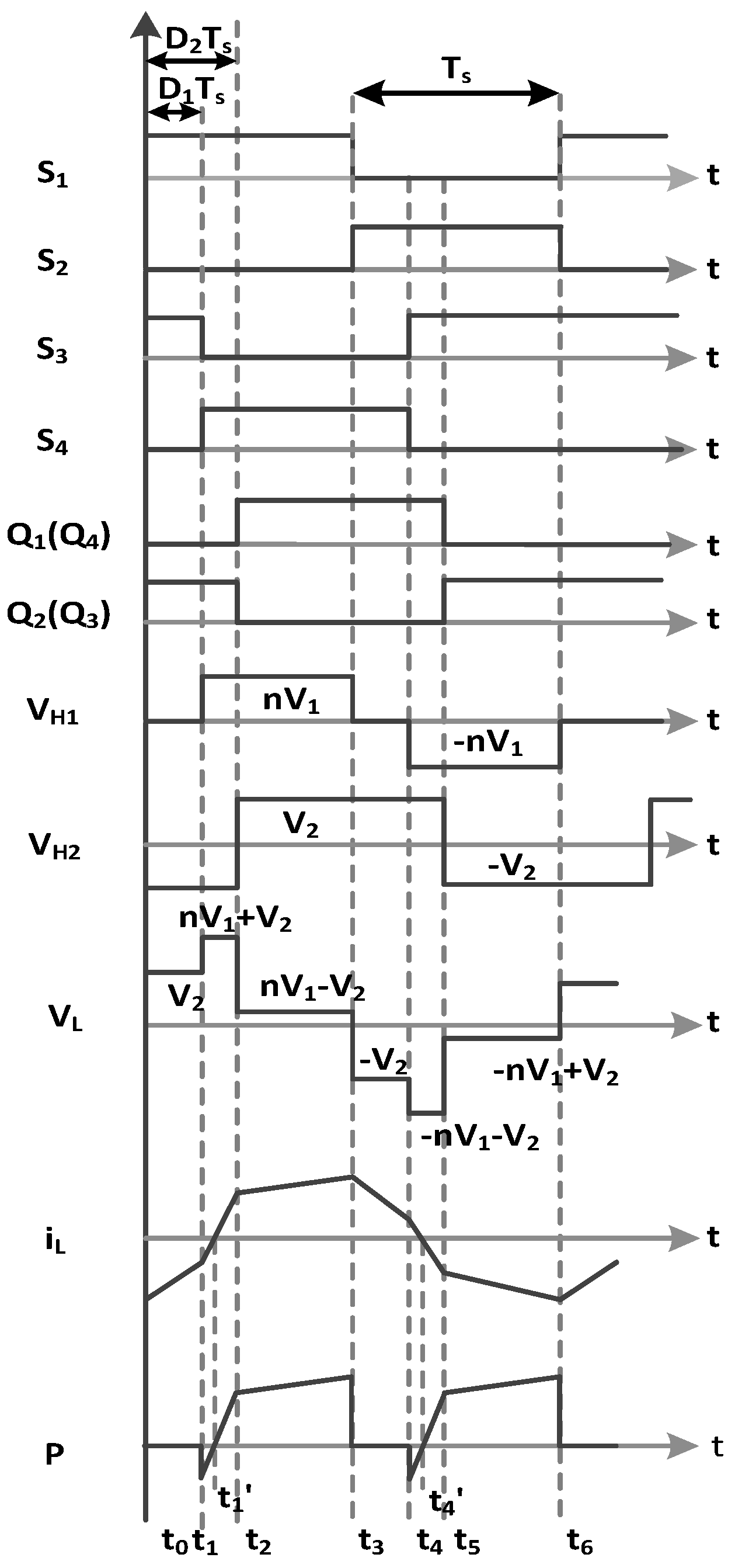
Figure 2 is the main circuit waveform including iL in a switching cycle. The VH1 and VH2 are the primary side voltage and secondary side voltage of high frequency transformers in Figure 2. Align equations and symbols

2.1. Steady State Performance Analysis

According to the principle of current ampere second equilibrium, the average of the inductance current is 0 within a switching period:
0 2 T S i L ( t ) d t = 0
The peak current of each time point can be derived from Figure 2:
{ i 0 = i L ( t 0 ) = T s 2 L ( n V 1 D 1 n V 1 2 V 2 D 2 + V 2 ) i 1 = i L ( t 1 ) = T s 2 L ( n V 1 D 1 n V 1 + 2 V 2 D 1 2 V 2 D 2 + V 2 ) i 2 = i L ( t 2 ) = T s 2 L ( n V 1 D 1 + 2 n V 1 D 2 n V 1 + V 2 ) i 3 = i L ( t 3 ) = T s 2 L ( n V 1 D 1 + n V 1 + 2 V 2 D 2 V 2 ) i 4 = i L ( t 4 ) = T s 2 L ( n V 1 D 1 + n V 1 2 V 2 D 1 + 2 V 2 D 2 V 2 ) i 5 = i L ( t 5 ) = T s 2 L ( n V 1 D 1 2 n V 1 D 2 + n V 1 V 2 )
Because the magnitude of the effective current of inductor current directly affects the copper consumption of transformer and the state loss of semiconductor device [22], it is necessary to derive the expression of the RMS value square of inductance current as follows:
i L ( r m s ) 2 = 1 2 T s 0 2 T s i L 2 ( t ) d t = T s 2 6 L 2 { D 1 ( n V 1 D 1 n V 1 D 2 V 2 D 2 ) ( n V 1 D 1 + 2 n V 1 D 2 3 n V 1 + 2 V 2 D 1 4 V 2 D 2 + 3 V 2 ) + D 2 ( n V 1 D 1 n V 1 + V 2 D 1 2 V 2 D 2 + V 2 ) ( n V 1 D 1 2 n V 1 D 2 + n V 1 2 V 2 D 1 V 2 ) + 1 2 [ ( n V 1 D 1 + 2 n V 1 D 2 n V 1 + V 2 ) 2 + ( n V 1 D 1 + n V 1 + 2 V 2 D 2 V 2 ) 2 + ( n V 1 D 1 + 2 n V 1 D 2 n V 1 + V 2 ) ( n V 1 D 1 + n V 1 + 2 V 2 D 2 V 2 ) ] }
In order to reduce the loss of the converter, the minimum RMS value of inductance current was chosen as one of the optimization objective functions.
The average output power can be calculated as follow:
P O = 1 T s 0 T s V H 1 i L ( t ) d t = n V 1 V 2 T s 2 L ( 2 D 1 D 2 2 D 2 2 + 2 D 2 D 1 2 D 1 )
and it can be concluded that, when D1 = 0, D2 = 0.5, the maximum average output power is:
P m a x = n V 1 V 2 8 f s L
When the output load is R, PO can also be expressed as:
P O = V 2 2 R
Combining with Equation (4) we can obtain:
V 2 = n V 1 R 4 f s L ( 2 D 1 D 2 2 D 2 2 + 2 D 2 D 1 2 D 1 )
I 2 = n V 1 4 f s L ( 2 D 1 D 2 2 D 2 2 + 2 D 2 D 1 2 D 1 )
Because the DAB converter requires 28 V DC voltage output, V2 = 28 V will be one of the constraints of this optimization model.

2.2. Reverse Power and Transient DC Bias Component Analysis
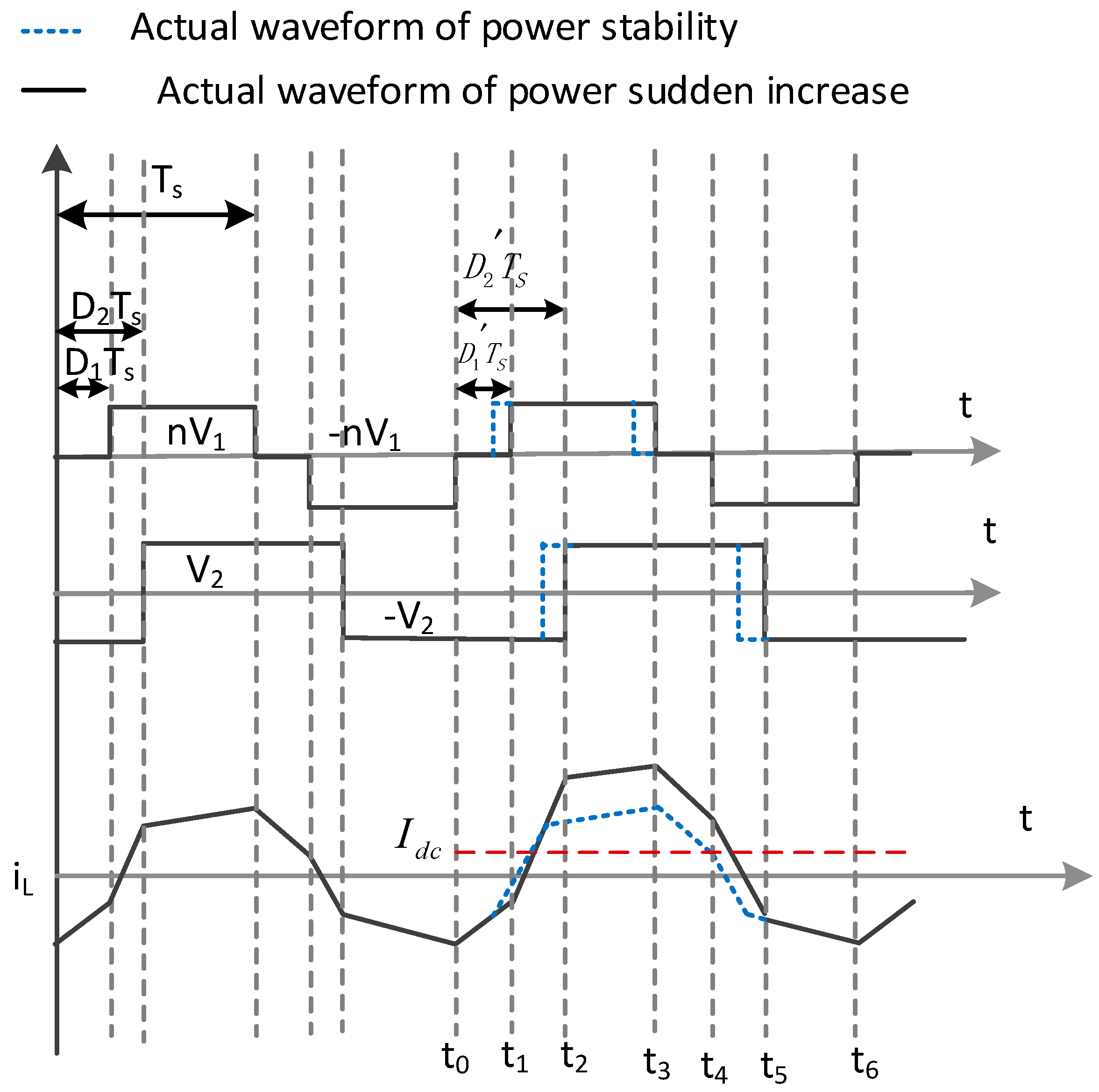
It can be seen from Figure 2 that in the power transmission process, negative power has a reverse power flow direction. The negative power is a kind of reactive power, it increases the apparent power of the power transmission process in the circuit, meanwhile the losses of the circuit and devices are also increased. The increase of the power loss of the whole power converter can further reduce the efficiency of power transmission of the DAB converter. When the reverse negative power decreases, the peak value of the transmitted power also decreases, which reduces the switching stress of the power switching device and reduces the demand for the high frequency transformer capacity and thus reduces the power volume of the transformer under design. Therefore, in order to improve the performance of the converter, it is necessary to reduce the reverse negative power of the converter as much as possible.
Deduce the time t 1 of the inductance current iL is 0, that is:
n V 1 + V 2 L t 1 t 1 + i ( t 1 ) = 0
We obtain:
t 1 = ( n V 1 D 1 + n V 1 + 2 V 2 D 2 V 2 ) T s 2 ( n V 1 + V 2 )
The reverse negative power can be obtained from this:
P a v g = 1 T s t 1 t 1 n V 1 | i L ( t ) | d t
Bring Equation (10) into Equation (11) and can be obtained:
P a v g = n V 1 T s 8 L ( n V 1 + V 2 ) [ n V 1 ( 1 D 1 ) + V 2 ( 2 D 2 2 D 1 1 ) ] 2
It can be seen that we can suppress the reverse negative power by optimizing the combination of D1 and D2, thus we choose Pavg minimum as one of the optimization objective functions.
In the circuit operating process, because of the difference of the parameters of the components or the asymmetry of circuit layout, the on-state voltage drop is not equal , the difference of the turn off time when the power switch is turned off, the power transistor trigger factors of pulse signal is asymmetric, and the current waveform of the high frequency transformer in the DAB converter cannot have ideal symmetry, therefore, the dc bias becomes a practical issue because of the inconsistency between theory and practice. According to these factors, the magnetization curve of the iron core is not symmetric about the origin of coordinates, and the magnetization curve is usually a nonlinear curve, so when there is very serious dc bias current, iron core will enter a saturation state, causing the magnetizing current to increase significantly, thus increasing the loss of the converter and even causing damage to the switching device [23,24,25].
Therefore, it is necessary to analyze and suppress this bias component. According to [16], the expression of DC bias is deduced to be used for subsequent suppression. The converter in positive mode (in buck mode), using a sudden increase in output power as an example, as shown in Figure 3, t0 moments ago, the converter stability and inductor current waveform were symmetrical, at time t0, with a power surge, if the converter internal and external shift duty noted before the power surge are D1 and D2, respectively, after the power mutation, the converter internal and external shift duty ratio are refreshed to D 1 and D 2 respectively, 0 < D 1 < D 1 and 0 < D 2 < D 2 , then, with the increase of phase angle, the maximum value of the inductor current increases, and the DC bias component will exist for even a few cycles.
DC bias component can be calculated according to the first cycle of:
I d c = 1 2 T s 0 2 T s i L ( t ) d = 2 T s L [ n V 1 ( D 1 D 1 ) + 2 V 2 ( D 2 D 2 ) ]
After the analysis above, this paper will select the minimum Idc as one of the optimization objective functions.
In order to realize the high frequency, high efficiency and low loss operation for the converter, soft switching technology is often used. The requirements of the DAB converter to implement ZVS are:
{ i ( t 1 ) 0 i ( t 2 ) 0
Substituting Equation (2) into Equation (14), and the following simplification can be obtained:
{ n V 1 D 1 n V 1 + 2 V 2 D 1 2 V 2 D 2 + V 2 0 n V 1 D 1 + 2 n V 1 D 2 n V 1 + V 2 0
Equation (15) will be considered as the constraint condition of the optimization model.
According to the requirements of Table 1, some function 3-D diagrams are drawn as follows.
From Figure 4a, it can be seen that under the premise of D 1 < D 2 < 1 , the closer the D1 and D2 are, the smaller the i L ( r m s ) 2 is. This result can be used as one of the screening bases for the D1 and D2 combination.
Figure 4b proves that when D1 = 0, D2 = 0.5
P m a x = n V 1 V 2 8 f s L = 583 W
It can be seen in Figure 4c, that when 0 < D 1 < 0.6 , 0.1 < D 2 < 1 , Idt is smaller this range can be used as one of the screening criteria.
As can be seen from Figure 4d, each PO corresponds to many i L ( r m s ) 2 , so it is necessary to limit i L ( r m s ) 2 . According to the rightmost point of the image, i L ( r m s ) 2 should not exceed 1000 when solving the optimization model. This result will be used as an additional constraint.

3. The Optimal Solution of Power Model of DAB Converter

Based on the above analysis, the optimization model of the DAB converter based on the extended phase shift control can be obtained according to the above analysis.
Design variables: the interior angle x 1 = D 1 , and the external angle x 2 = D 2 , where: k 1 = T S = 1 / 80000 , k 2 = 1.2 e 5 , k 3 = n V 1 = 80 , k 4 = V 2 = 28 , k 5 = P 0 = 500 .
Objective function:
min { f 1 ( x 1 , x 2 ) = k 1 2 6 k 2 2 { x 1 ( k 3 x 1 k 3 x 2 k 4 x 2 ) ( k 3 x 1 + 2 k 3 x 2 3 k 3 + 2 k 4 x 1 4 k 4 x 2 + 3 k 4 ) + x 2 ( k 3 x 1 k 3 + k 4 x 1 2 k 4 x 2 + k 4 ) ( k 3 x 1 2 k 3 x 2 + k 3 2 k 4 x 1 k 4 ) + 1 2 [ ( k 3 x 1 + 2 k 3 x 2 k 3 + k 4 ) 2 + ( k 3 x 1 + k 3 + 2 k 4 x 2 k 4 ) 2 + ( k 3 x 1 + 2 k 3 x 2 k 3 + k 4 ) ( k 3 x 1 + k 3 + 2 k 4 x 2 k 4 ) ] } f 2 ( x 1 , x 2 ) = k 3 k 1 8 k 2 ( k 3 + k 4 ) [ k 3 ( 1 x 1 ) + k 4 ( 2 x 2 2 x 1 1 ) ] 2 f 3 ( x 1 , x 2 ) = 2 k 1 k 2 [ k 3 ( x 1 x 1 ) + 2 k 4 ( x 2 x 2 ) ]
Constraints:
{ 0 < x 1 < x 2 < 1 f 1 ( x 1 , x 2 ) < 1000 k 3 x 1 + 2 k 3 x 2 k 3 + k 4 0 k 3 x 1 k 3 + 2 k 4 x 1 2 k 4 x 2 + k 4 0 k 3 k 4 k 1 2 k 2 ( 2 x 1 x 2 2 x 2 2 + 2 x 2 x 1 2 x 1 ) = k 5
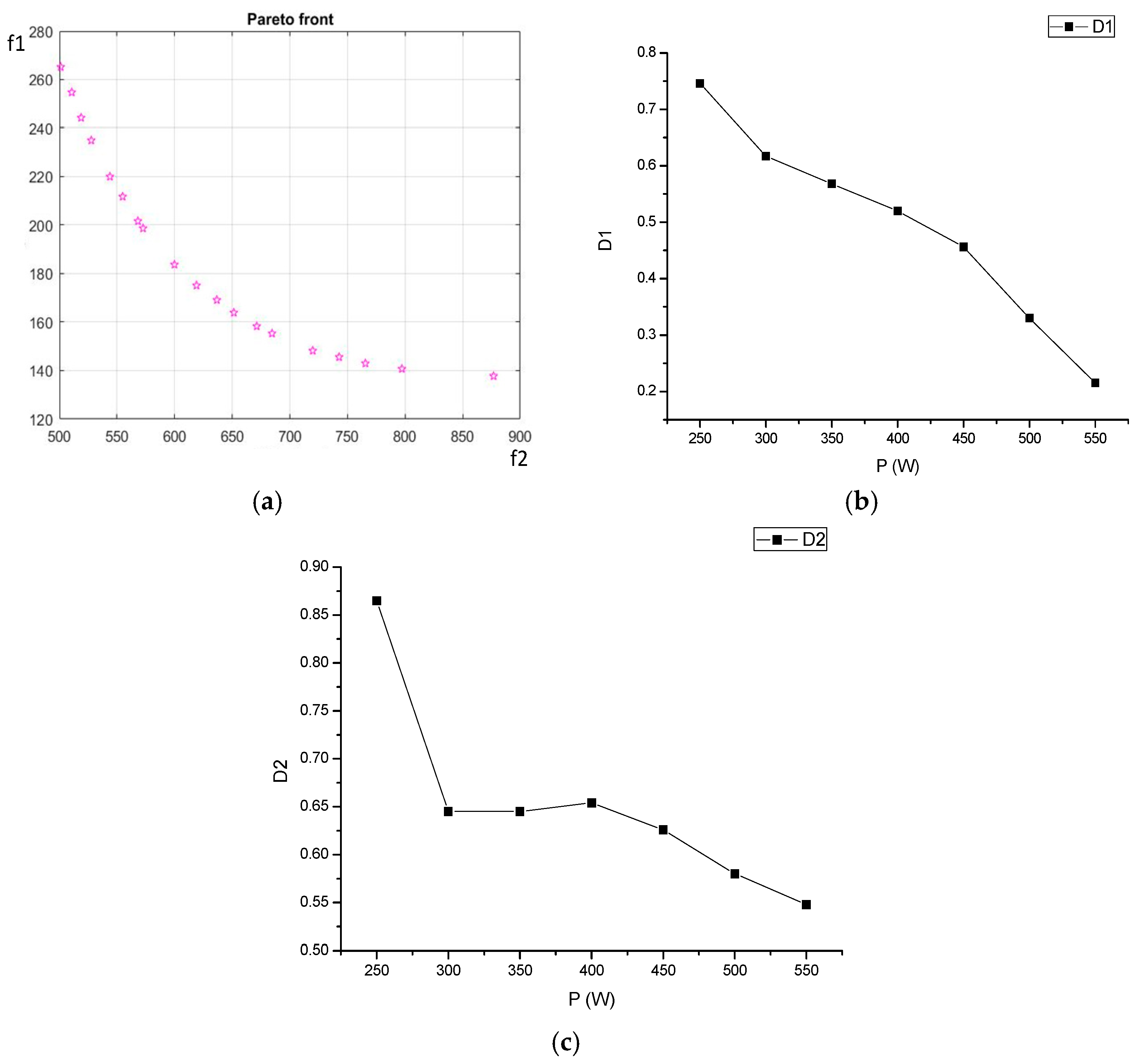
Genetic algorithm is an adaptive probability optimization algorithm that solves complex system optimization problems with the help of biological genetics and evolutionary ideas. It does not depend on the research object. Using the multi-objective genetic algorithm in the MATLAB genetic algorithm toolbox, the above models are solved, and a set of internal and external phase shift angles corresponding to the variation of load power are obtained, which is shown in Table 2. The Toolbox’s configuration is shown in following: Solver: gamultiobj; Population size: 1000; Pareto front population fraction: 0.02; Generations: 1000; Function tolerance: 1e-8; Constraint tolerance: 0.01. All the variables and parameters must be normalized. The Pareto front curve for the rated conditions is shown in Figure 5a. The terms f1 and f2 respectively correspond to the optimized objects. That is the optimization result, which is an important basis for our subsequent simulation and experiments. According to the Table 2, the basic relationship between the load power and phase shift angle D1, D2 can be as shown in Figure 5b,c.

4. Simulation Verification

4.1. MATLAB Simulation Verification

According to the parameters in Table 1, a DAB converter model based on MATLAB/Simulink is fully run for 0.1 s, whereby the load resistance increases from 1.568 Ω to 3.136 Ω at 0.05 s, and the transmission power is changed from the rated 500 W to 250 W, comparing the performance indexes of DAB converter, in contrast to the traditional proportion integration differentiation (PID) control mode. The closed-loop control blocks for the DAB converters can be realized by the look-up table from the control variable of Table 2 under the different load situations by the offline optimization method, so the linear extrapolation methods algorithm can be used for the close-loop controller in look-up table to meet the power demand between the given load power points in Figure 2. The control block diagram of the DAB converter based on the optimal control methods is shown in Figure 6a and the flow chart of the control algorithm is shown in Figure 6b. From Figure 6a, the offline optimal phase shift variables D1 and D2 can be selected by the load power computation. The control algorithm based on the Figure 6b is very simple and high efficiency. It is very easily realized in the digital signal processing (DSP) controller platform.

4.1.1. Transient Output Characteristics

The output voltage, current waveform and local magnification diagram of the two control mode methods are shown in Figure 7.
One can get from the figures, on the optimal control model, that the response time of the converter is 6 ms, output voltage is stable at 28 V, output current is about 17.86 A, power is 500 W, the system has no overshoot during start-up, voltage ripple is less than 0.1 V, and the ripple ratio is less than 0.36%. When the load mutates, the output voltage has a 0.1 V overshoot with a rate of about 0.3%, then settles at 27.7 V, about 1% error, ripple about 0.06 V, with a rate of about 0.2%. In the traditional control mode, when the load is suddenly changed, the output voltage fluctuates rapidly between 27.6 V and 28.3 V. The ripple peak value reaches 0.7 V, and the ripple ratio is about 2.5%, which seriously affects the stability of the converter output.

4.1.2. RMS Value of Inductor Current and DC Bias Current Component

In the two control modes, the waveforms of the inductance current are as shown in Figure 8.
It can be seen from the above diagrams that the peak value of inductance current increases from 60 A to 65 A in the traditional control mode when the load is changed. The inductance current waveform is shifted upwards, the forward amplitude is about 40 A, and the negative amplitude is about −25 A, and no longer has positive and negative symmetry. In the optimal control mode, the current waveform of the inductor still shows positive and negative symmetry, the peak-to-peak value decrease obviously, from 60 A to 40 A, and the positive and negative amplitude is about 20 A. At the same time, through the MATLAB/Simulink module solution, the RMS value of the inductor current of traditional control mode is 19.91 A, the DC bias component is about 1.146 A, and for the optimal control mode, the RMS value of the inductor current is 16.86 A, the DC bias component is about 0.4893 A, and one can see that the two indexes of the RMS value of the inductor current and DC bias component are significantly improved in optimal control mode compared with the traditional PI control.

4.1.3. Reverse Negative Power

The waveform of the transient power of the low voltage side of the transformer under two control modes is shown in Figure 9.
It can be clearly seen that under optimizing control mode, negative power was inhibited to almost 0, while under the traditional control mode, the negative power did not fall, therefore, the index of negative power is also significantly improved under optimal control.

4.1.4. Comparison and Summary of the Changes

The other situations are similar to the result of Figure 7a,b. In Table 3, we directly give the comparison of three indexes, ① is the optimization control mode, and ② is the traditional control mode.
Three contrastive curves are drawn in Figure 10 from Table 3: (the transverse axis indicates a transient variation from the rated power of 500 W to the corresponding power).
The comparison in Figure 10 shows that, under the rated power, the indicators of the two kinds of control modes are similar, but when the load changes, the performance index of the optimized control mode is obviously superior to the traditional control mode.

4.2. Typhoon Hard-in-Loop Simulation Verification

The Typhoon HIL system provides a complete solution to engineers doing research and design of power electronics systems on one system (platform) for engineering project design, real-time simulation, verification and real-time testing. Figure 11a is the hardware block diagram of the Typhoon HIL system [26].
The main circuit of the system is built on the Typhoon platform, as shown in Figure 11b, and the semi physical simulation experiment is carried out in combination with the control program in the DSP28335 (Delfino, Texas Instruments, Dallas, TX, USA). Like the MATLAB simulation, the load resistance increases from 1.568 Ω to 3.136 Ω at 0.05 s, and the transmission power is changed from the rated 500 W to 250 W. Observe the performance under the load transient variation.

4.2.1. Output Voltage Performance

The DAB converter is connected with pure resistive load in accordance with the parameters given in Table 1. The waveform at the output terminal of DAB converter is shown in Figure 12a under the rated steady state. The red waveform represents the output voltage. The green one is output current waveform.
It is shown that the converter response time is about 7 ms, there is no overshoot and output voltage is stable at 28 V, ripple voltage is about 0.04 V, the ripple ratio is 0.14%, output current is about 17.86 A, the current ripple is about 0.04 A, the ripple ratio is 0.22%, output power reaches 500 W, reached the requirements.
After the load is abruptly changed, the output voltage and current waveform are shown in Figure 12b. After the load transient variation, the voltage drops slightly, but it remains near 28 V, the current is about 8.86 A, and the power is about 250 W.

4.2.2. Realization of Soft Switching

The operation of switch Q1 & S1 is shown in Figure 13. Figure 13a is the turn on waveform of S1. Under rated working conditions, the voltage VDS when the switch is off is 270 V, and the drive voltage of switch, VGS is 1 V. At the moment of S1 opening, the S2 has been turned off, the inductance current is negative, and the anti-parallel diode of S1, SD1 is used to continue the current, thus, the zero voltage opening conditions are met. The red waveform is the switching waveform of device S1 and Q1. The green one is the waveform of inductance current.
Figure 13b is the open waveform of Q1. Under rated working condition, the voltage VDS when the switch is off is 28 V, and the drive voltage of switch, VGS is 1 V. At the moment of Q1 opening, the Q2 has been turned off, the inductance current is negative, and the anti-parallel diode of Q1, QD1 is used to continue the current, thus, the zero voltage opening conditions are meet. The other switches are similar to the above waveforms, and therefore are omitted here.

4.2.3. Coupled Inductor Related Waveforms

Figure 14 is an inductive voltage waveform, which is in agreement with the theoretical analysis.
Figure 15a,b are the inductance current waveforms of the steady-state and load abrupt moments, which are same with the low voltage side current waveforms of transformer. As can be seen from Figure 15a, the current waveform of the inductor is in agreement with the theoretical analysis. As can be seen from Figure 15b, after the load is abruptly changed, the inductance current is restored to positive and negative symmetry after about 0.0004 s, and the peak and peak value decrease from ±30 V to ±20 V. By calculation the RMS value of the inductor current is 16.88 A, and the DC bias component is about 0.4903 A.

4.2.4. Transformer Related Waveform

Figure 16 is the voltage waveform of the low voltage side of the transformer, with an amplitude of ±80 V, and the waveform is consistent with the theoretical analysis.
Figure 17 is the power waveforms of the low voltage side of the transformer at the steady-state and load abrupt variation moments.
Due to the role of the external phase angle D2, the phase of the transformer's current and voltage is not synchronous in Figure 15a and Figure 16, which results in a negative value of the instantaneous power of the transformer, that is, the reverse negative power phenomenon. However, from Figure 16, we can see that because of the presence of D1, the output voltage has zero output time. In this period, the negative power has changed to 0, which reduces the size of negative power and improves the efficiency of energy transmission. It can be seen from Figure 17b that the reverse negative power is suppressed after the load mutation, and after 12 cycles, about 0.3 ms, the negative power is almost 0 W.

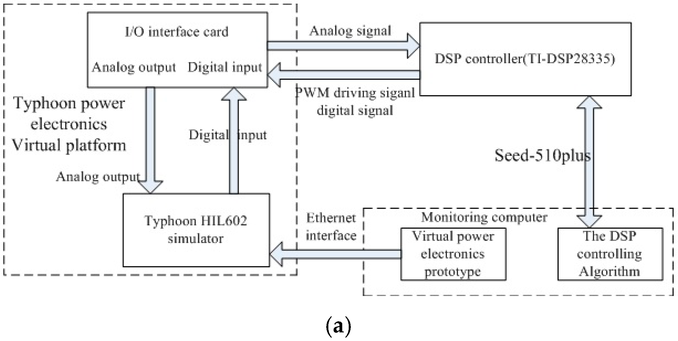
5. Verification of Experiment Prototype Hardware

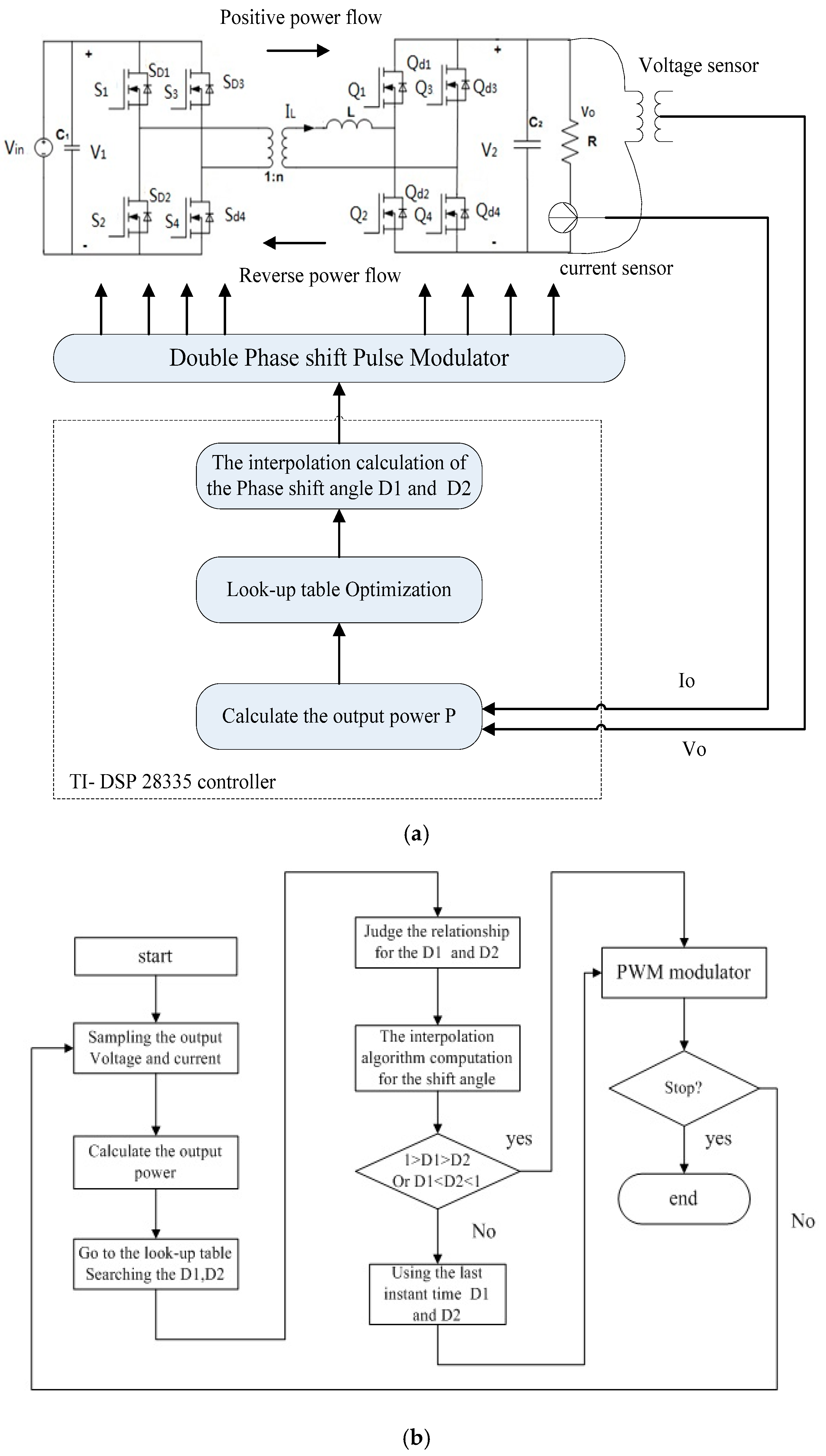
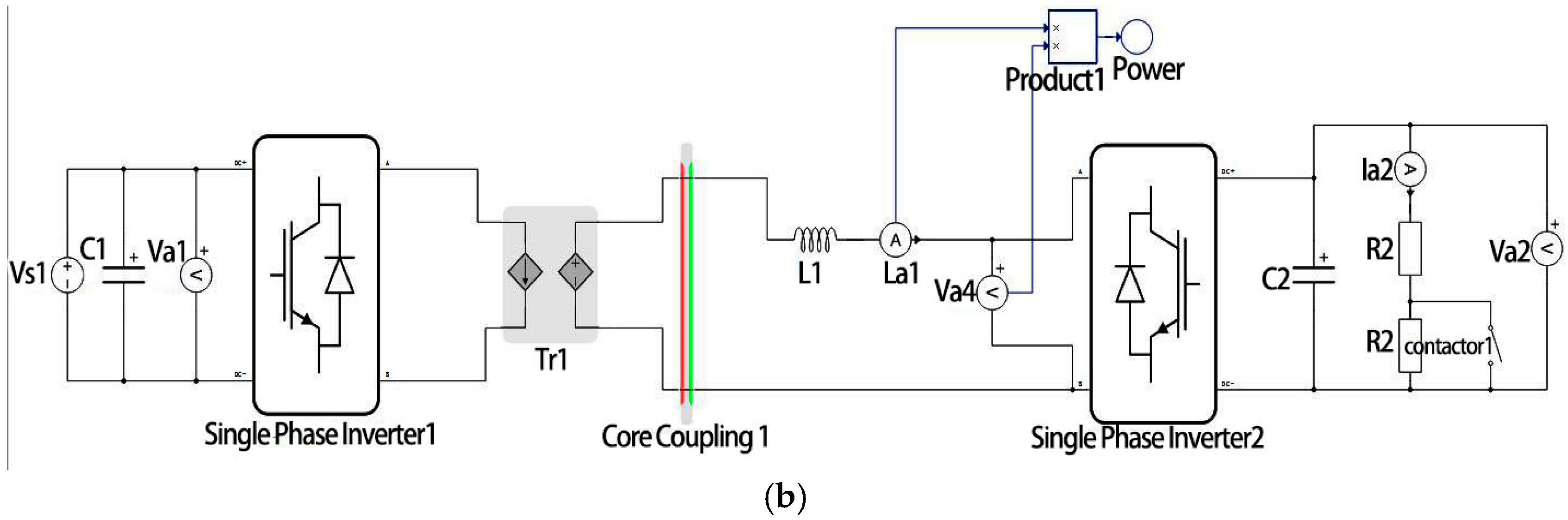
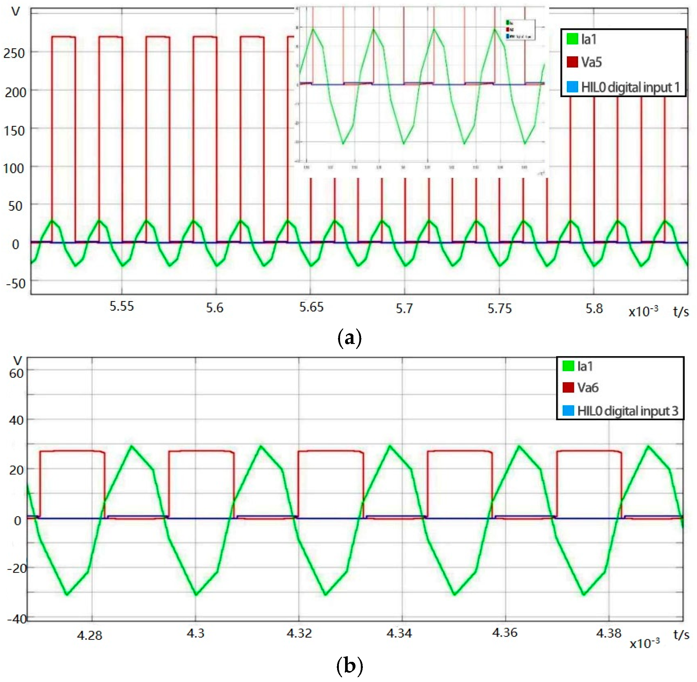
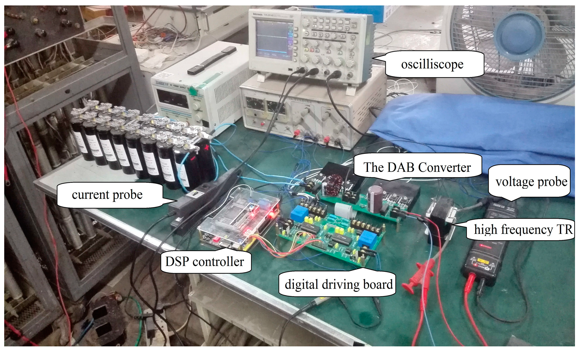
A prototype DAB converter was designed for verification of the proposed scheme. A 200–600 W scaled down DAB converter has been developed. The schematic layout of experimental set-up is presented in Figure 18. During the experimentation, an aerospace high voltage DC source (270 V DC) was used for power supply. In the DAB converter, the power switching device in high voltage side was a International Rectifier-MOSFET IRF460P (Infineon Technologies AG, Neubiberg, Germany), and on the low voltage side it is an IRF150P.
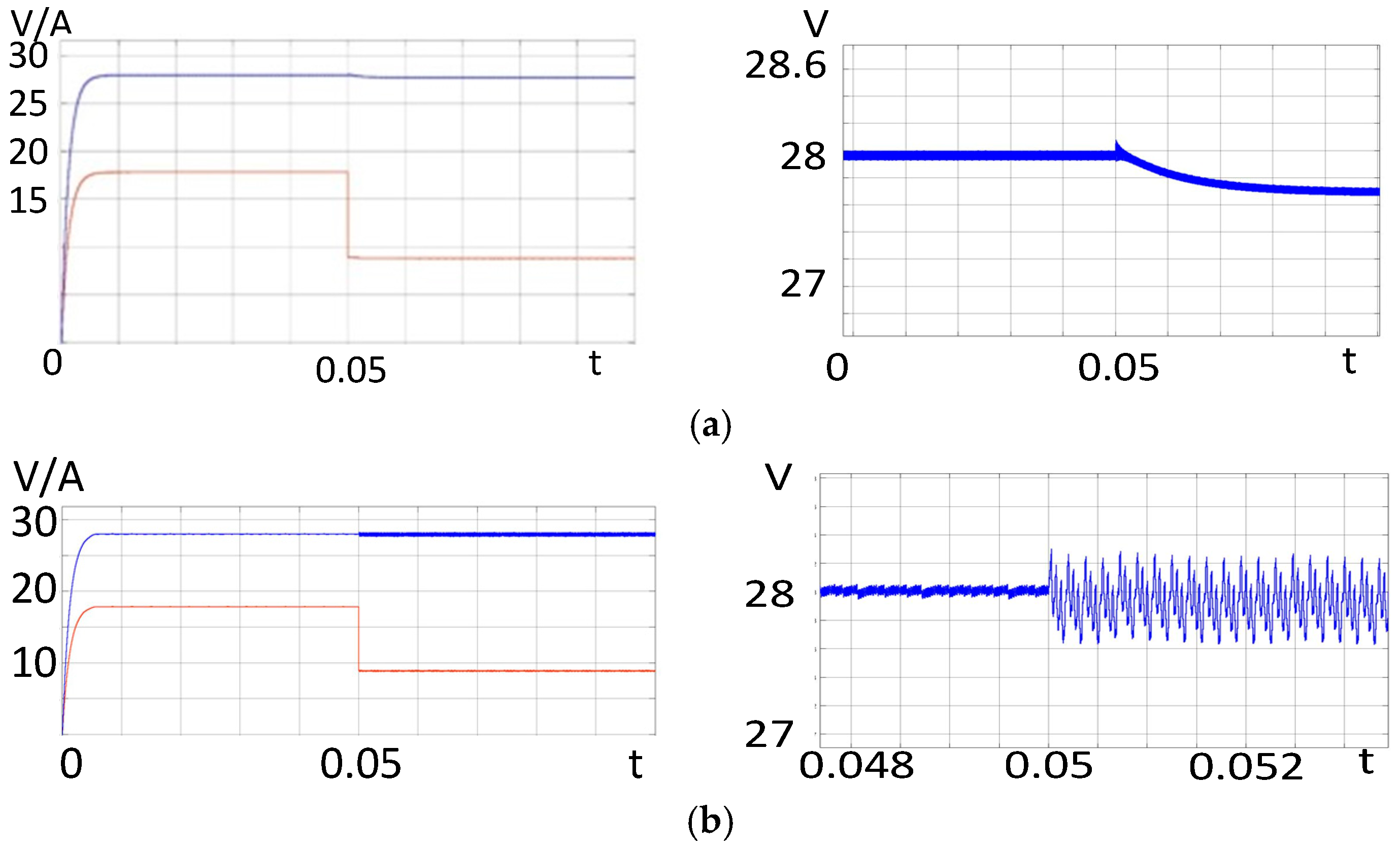
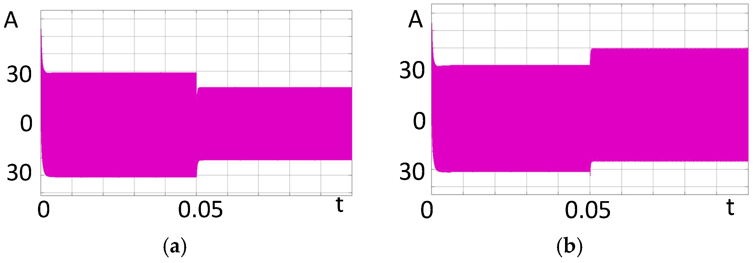
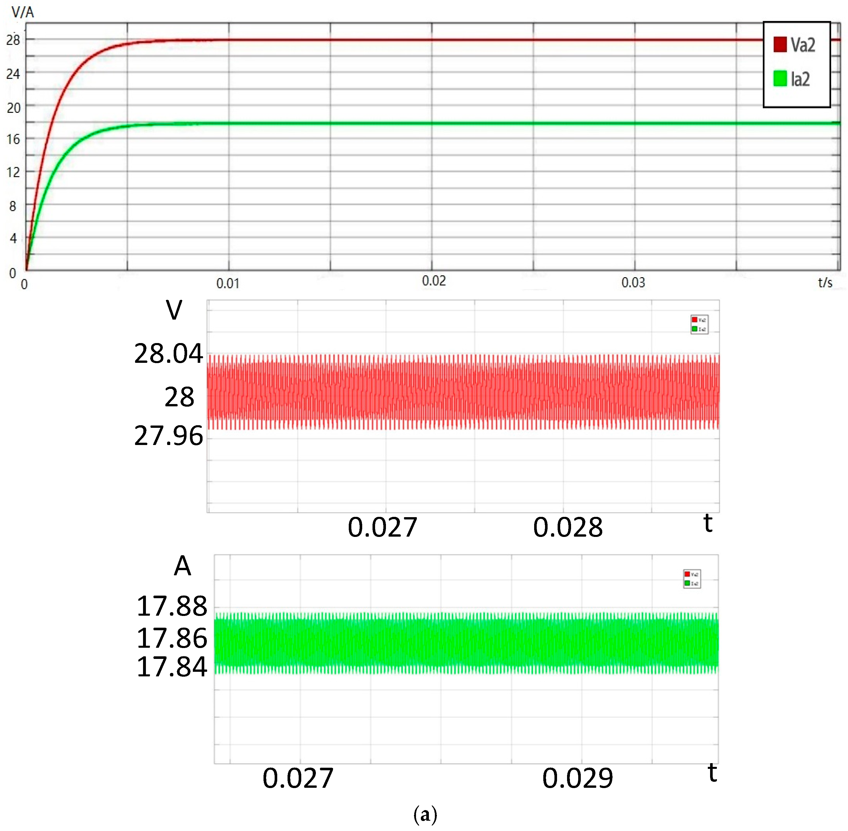
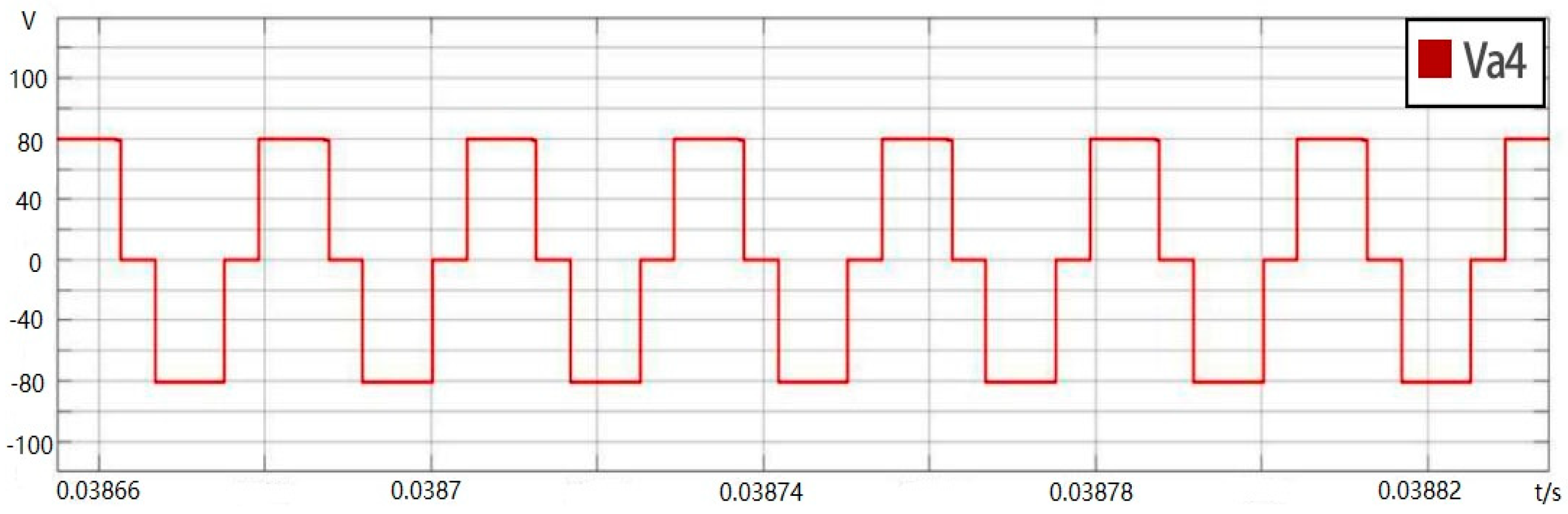
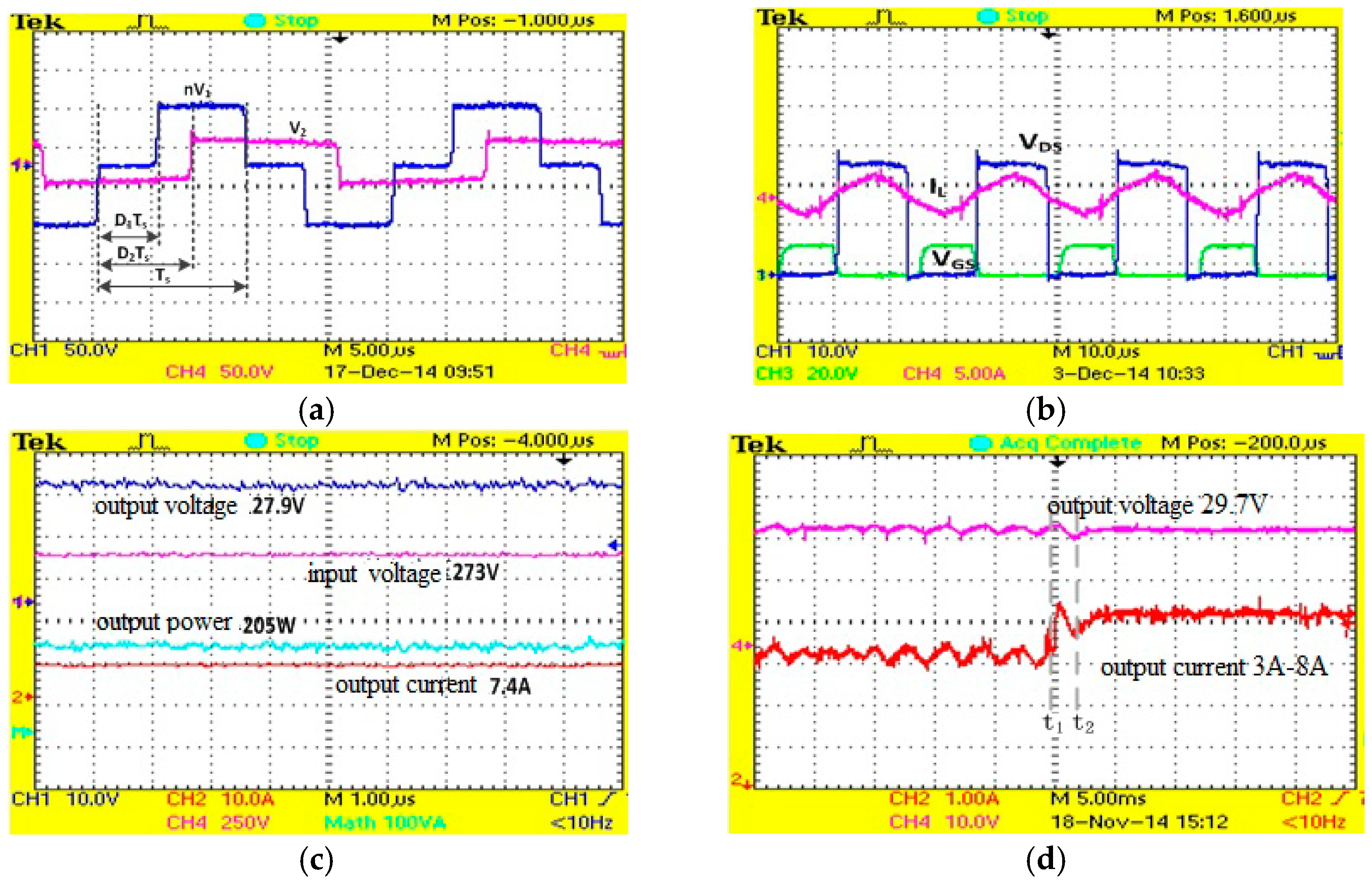
The experimental verification of DAB converter is carried out by using a DSP28335 DSP digital controller, All the control algorithms were downloaded into this controller. The results of the experiments are shown in Figure 19. From 
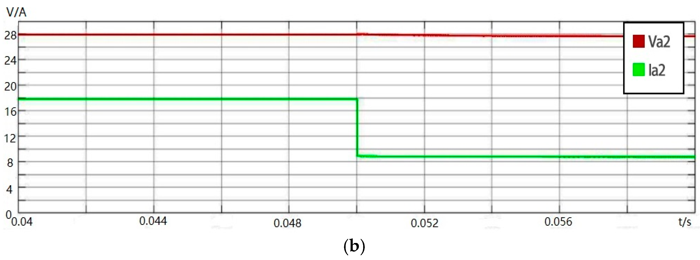
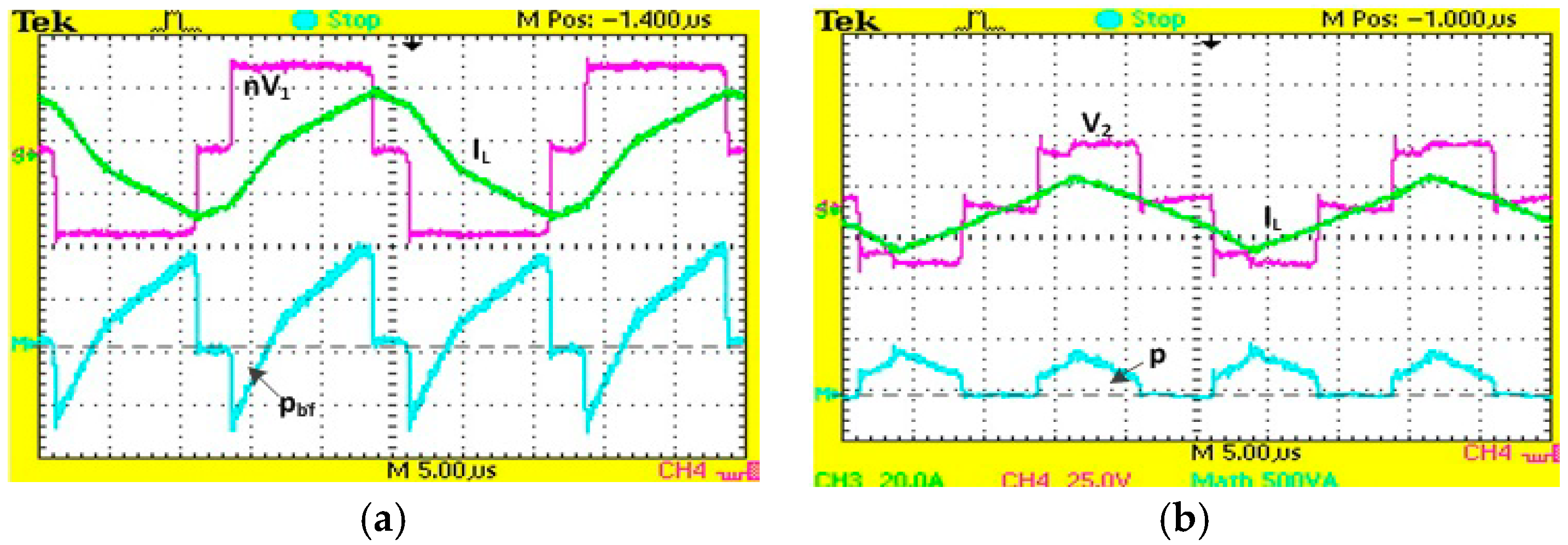
Figure 19a, the steady state characteristic for the output voltage can be achieved by the proposal controlling methods based on the multi-objective optimization. In 
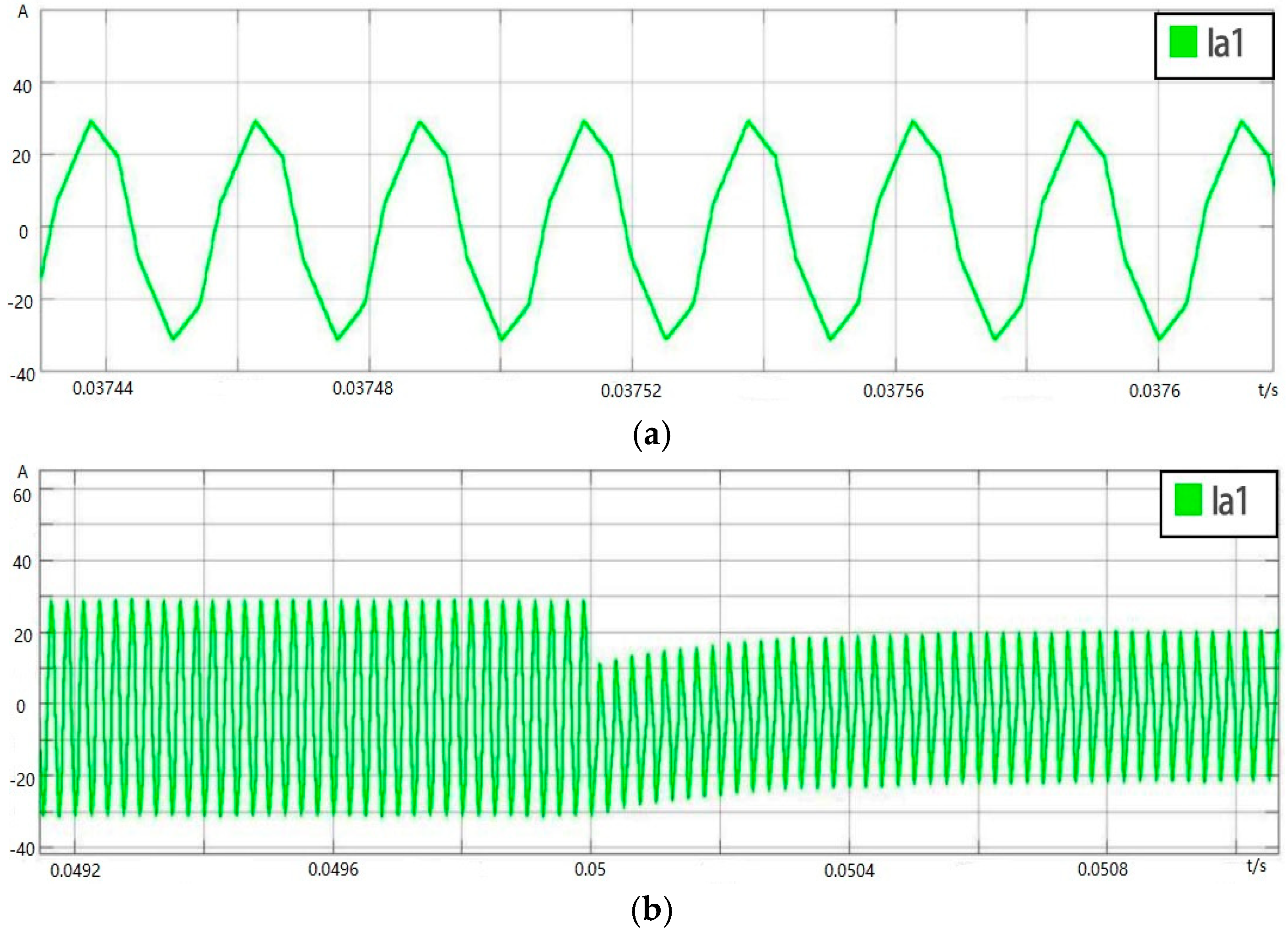
Figure 19b,c, it is can been seen that the inductance current can charge and discharge following the control logic signal under the optimization methods. The power transmission can be achieved according to Figure 19c. When the input voltage is 273 V, the output voltage is 27.9 V. In order to verify the transient ability of the control algorithm, the transient load variation was carried out, with the experimental results shown in Figure 19d, and the output voltage can be quickly kept at reference voltage of 28 V.
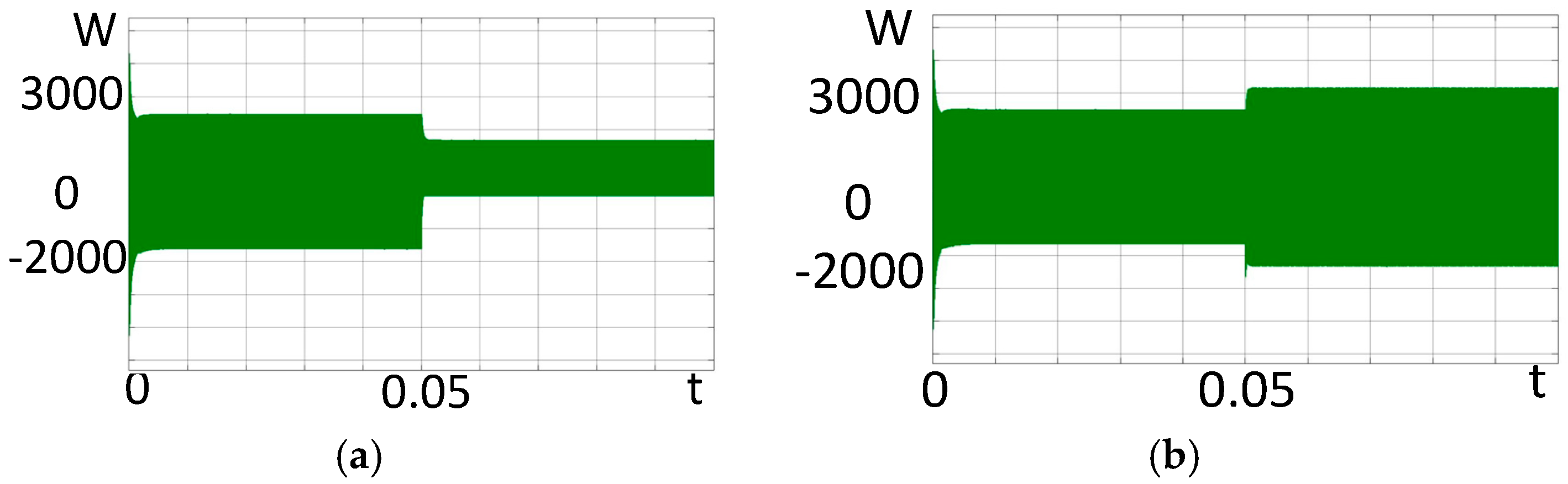
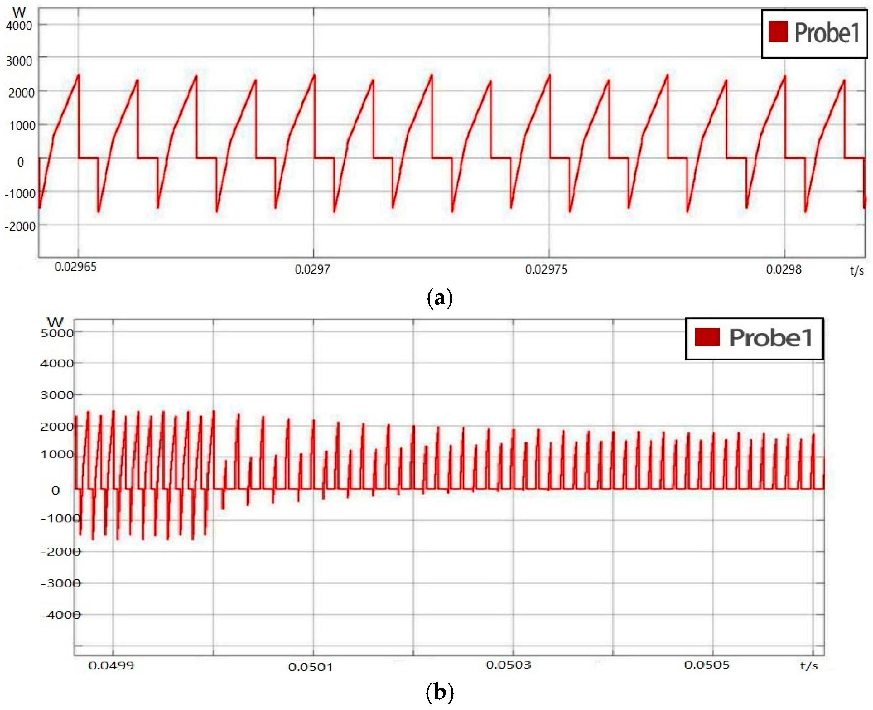
In order to verify the capability of the proposed method to decrease the reverse negative power transmission, a comparative experiment was carried out under the two control methods, for the traditional double phase shift and the proposed method, respectively. It can be seen from Figure 20 that the reverse negative power can be greatly reduced. It is verified that the proposed methods are valid and reliable enough for use in the DAB converter in an aircraft electric power system background.
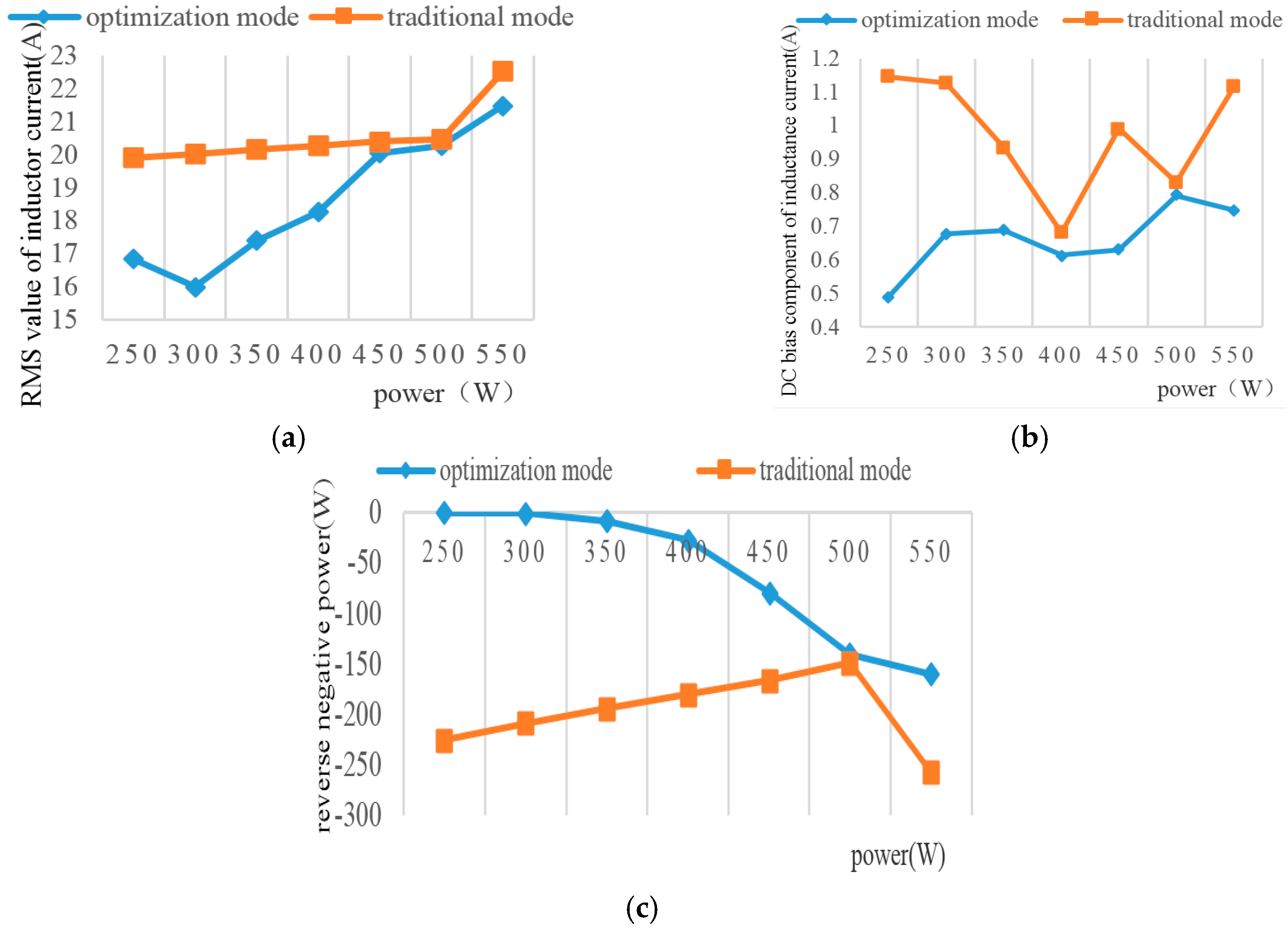
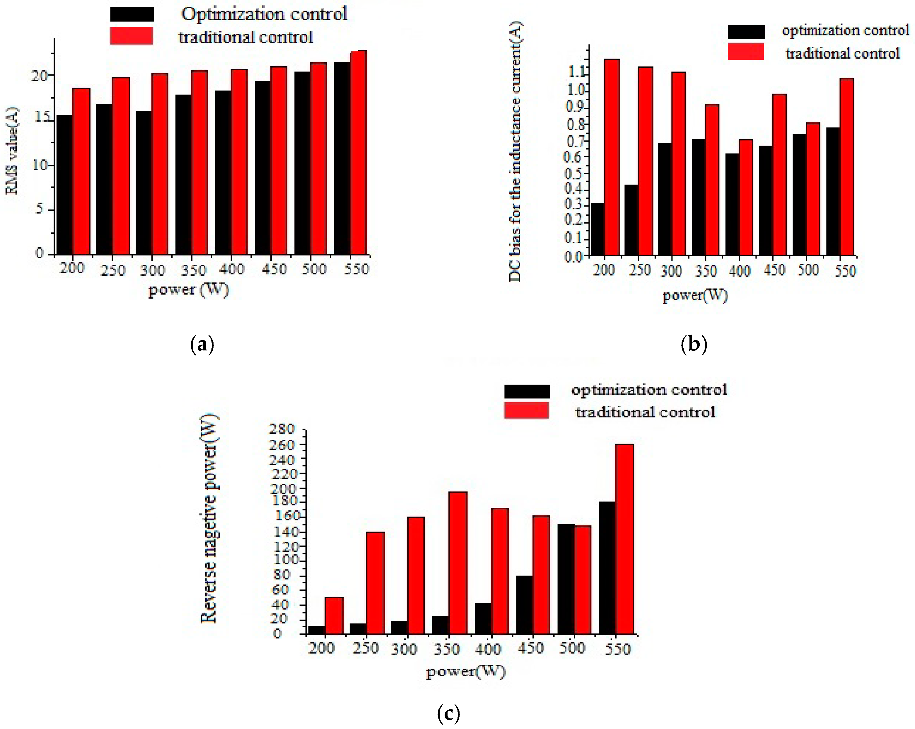
According to the different performance index testing methods, the aerospace DAB converter’s experimental result comparison under different control methods can be showed in Figure 21. From Figure 21, the DAB converter’s performance features such as the inductance current RMS can be minimized based on the optimization control method. The DC-bias current for the high frequency transformer can be suppressed greatly to avoid the saturation of the iron core of the transformer. The reverse negative power was also greatly reduced based on the optimization control methods, which can improve the efficiency of DAB converter. The experimental result can match the result from the simulation result.

6. Conclusions

Based on requirements of aviation, this paper designs a dual active bridge DC-DC converter with an extended phase shifting control strategy. The interior and external phase angle are used as the design variables, taking three indexes—the inductor current RMS, transformer reverse negative power and DC bias component—as the optimization goal. The optimization model is established with soft switching as the main constraint. The genetic algorithm optimization toolbox in MATLAB is used to solve the optimal control variable of the DAB converter optimization model. According to the results of simulation and experiments based on the MATLAB/Simulink platform, the Typhoon HIL platform and a hardware prototype, the three indexes have been effectively improved, and the rationality of the optimization method is verified. The next step for this research topic is to analyze the relationship between the different optimal objects, and simplify the optimal power model for the DAB converter. Based on this, the aim is to explore the real-time selection method of the optimal solution and realize online optimization control of the DAB converter.

Author Contributions

Tao Lei and Cengying Wu proposed the Multi-objective optimization control strategy; Cengying Wu build the simulation model for the DAB converter; Xaiofei Liu and Tao Lei performed the experiments for DAB converter; Cengying Wu and Tao Lei analyzed the simulation and experimental data; Tao Lei, Cengying Wu, and Xaiofei Liu wrote the paper.

Conflicts of Interest

The authors declare no conflict of interest.

References

  1. Boucher, R.J. Sunrise, the world’s first solar-powered airplane. J. Aircraft. 2015, 22, 840–846. [Google Scholar] [CrossRef]
  2. Ortiz, G.; Uemura, H.; Bortis, D.; Kolar, J.W.; Apeldoorn, O. Modeling of Soft-Switching Losses of IGBTs in High-Power High-Efficiency Dual-Active-Bridge DC/DC Converters. IEEE Trans. Electron Devices 2013, 60, 587–597. [Google Scholar] [CrossRef]
  3. Cougo, B.; Meynard, T.; Schneider, H. Reconfigurable Dual Active Bridge Converter for Aircraft Application. In Proceedings of the IEEE Electrical Systems for Aircraft, Railway and Ship Propulsion (ESARS), Bologna, Italy, 16–18 October 2012; pp. 1–6. [Google Scholar]
  4. Naayagi, R.T.; Forsyth, A.J.; Shuttleworth, R. High-power Bidrectional DC-DC Converter for Aerospace Applications. IEEE Trans. Power Electron. 2012, 27, 4366–4379. [Google Scholar] [CrossRef]
  5. Sarlioglu, B. Advances in AC-DC power conversion topologies for More Electric Aircraft. In Proceedings of the Transportation Electrification Conference and Expo, Dearborn, MI, USA, 18–20 June 2012; pp. 1–6. [Google Scholar]
  6. Naayagi, R.T. A review of more electric aircraft technology. In Proceedings of the International Conference on Energy Efficient Technologies for Sustainability, Nagercoil, India, 10–12 April 2013; pp. 750–753. [Google Scholar]
  7. Engel, S.P.; Soltau, N.; Stagge, H.; De Doncker, R.W. Dynamic and Balanced Control of Three-Phase High-Power Dual-Active Bridge DC-DC Converters in DC-Grid Applications. IEEE Trans. Power Electron. 2013, 28, 1880–1889. [Google Scholar] [CrossRef]
  8. Zhao, B.; Yu, Q.; Sun, W. Extended-Phase-Shift Control of Isolated Bidirectional DC–DC Converter for Power Distribution in Microgrid. IEEE Trans. Power Electron. 2012, 27, 4667–4680. [Google Scholar] [CrossRef]
  9. Krismer, F.; Kolar, J.W. Closed Form Solution for Minimum Conduction Loss Modulation of DAB Converters. IEEE Trans. Power Electron. 2011, 27, 174–188. [Google Scholar] [CrossRef]
  10. Krismer, F.; Kolar, J.W. Efficiency-Optimized High-Current Dual Active Bridge Converter for Automotive Applications. IEEE Trans. Ind. Electron. 2012, 59, 2745–2760. [Google Scholar] [CrossRef]
  11. Shen, Y.; Sun, X.; Li, W.; Wu, X.; Wang, B. A Modified Dual Active Bridge Converter with Hybrid Phase-Shift Control for Wide Input Voltage Range. IEEE Trans. Power Electron. 2016, 31, 6884–6900. [Google Scholar] [CrossRef]
  12. Choi, W.; Rho, K.M.; Cho, B.H. Fundamental Duty Modulation of Dual-Active-Bridge Converter for Wide-Range Operation. IEEE Trans. Power Electron. 2016, 31, 4048–4064. [Google Scholar] [CrossRef]
  13. Taylor, A.; Liu, G.; Bai, H.; Brown, A.; Johnson, P.M.; McAmmond, M. Multiple-Phase-Shift Control for Dual Active Bridge to Secure Zero-Voltage Switching and Enhance Light-Load Performance. IEEE Trans. Power Electron. 2018, 33, 4584–4589. [Google Scholar] [CrossRef]
  14. Tong, A.; Hang, L.; Li, G.; Jiang, X.; Gao, S. Modeling and Analysis of Dual-Active-Bridge Isolated Bidirectional DC/DC Converter to Minimize RMS Current. IEEE Trans. Power Electron. 2018, 33, 5302–5316. [Google Scholar] [CrossRef]
  15. Filba-Martinez, A.; Busquets-Monge, S.; Nicolas-Apruzzese, J.; Bordonau, J. Operating Principle and Performance Optimization of a Three-Level NPC Dual-Active-Bridge DC-DC Converter. IEEE Trans. Ind. Electron. 2016, 63, 678–690. [Google Scholar] [CrossRef]
  16. Zhao, B.; Song, Q.; Liu, W.; Sun, W. Current-Stress-Optimized Switching Strategy of Isolated Bidirectional DC–DC Converter With Dual-Phase-Shift Control. IEEE Trans. Ind. Electron. 2013, 60, 4458–4467. [Google Scholar] [CrossRef]
  17. Akter, P.; Uddin, M.; Mekhilef, S.; Tan, N.M.L.; Akagi, H. Model predictive control of bidirectional isolated DC-DC converter for energy conversion system. Int. J. Electron. 2015, 102, 1407–1427. [Google Scholar] [CrossRef]
  18. Saeed, J.; Hasan, A. Unit Prediction Horizon Binary Search-Based Model Predictive Control of Full-Bridge DC-DC Converter. IEEE Trans. Control Syst. Technol. 2018, 26, 463–473. [Google Scholar] [CrossRef]
  19. Tong, A.; Hang, L.; Guojie, L.I. Global Optimized Control Strategy of Dual Active Bridge Converter Controlled by Triple-phase-shift Modulation Scheme and Its Analysis. Proc. CSEE 2017, 37, 6037–6049. [Google Scholar]
  20. Burkart, R.M.; Kolar, J.W. Comparative η-ρ-σ Pareto Optimization of Si and SiC Multilevel Dual-Active-Bridge Topologies with Wide Input Voltage Range. IEEE Trans. Power Electron. 2017, 32, 5258–5270. [Google Scholar] [CrossRef]
  21. Chakraborty, S.; Chattopadhyay, S. Minimum-RMS-Current Operation of Asymmetric Dual Active Half-Bridge Converters with and Without ZVS. IEEE Trans. Power Electron. 2017, 32, 5132–5144. [Google Scholar] [CrossRef]
  22. Zhang, K.; Shan, Z.; Jatskevich, J. Large- and Small-Signal Average Value Modeling of Dual-active-bridge DC–DC Converter Considering Power Losses. IEEE Trans. Power Electron. 2017, 32, 1964–1974. [Google Scholar] [CrossRef]
  23. Zhao, B.; Song, Q.; Liu, W. Efficiency Characterization and Optimization of Isolated Bidirectional DC-DC Converter Based on Dual-Phase-Shift Control for DC Distribution Application. IEEE Trans. Power Electron. 2013, 28, 1711–1727. [Google Scholar] [CrossRef]
  24. Shao, C.W.; Wang, S.Z. Function Analysis of Biasing and Its Restriction Technique in Full Bridge Converter. Electrotech. Electr. 2012, 1, 4. [Google Scholar]
  25. Zhao, B.; Song, Q.; Liu, W.; Zhao, Y. Transient DC Bias and Current Impact Effects of High-Frequency-Isolated Bidirectional DC-DC Converter in Practice. IEEE Trans. Power Electron. 2016, 31, 3203–3216. [Google Scholar] [CrossRef]
  26. Typhoon HIL 600 User Manual. Available online: https://www.typhoon-hil.com/products/hil604 (accessed on 19 May 2016).
Figure 1. The topology of a DAB converter.
Energies 11 01168 g001
Figure 2. The main circuit waveform in one cycle.
Energies 11 01168 g002
Figure 3. Basic waveforms before and after power changing dynamically.
Energies 11 01168 g003
Figure 4. Function 3-D diagrams according to Table 1. (a) Function diagram of D 1 D 2 i L ( r m s ) 2 ; (b) Function diagram of D 1 D 2 P 0 ; (c) Function diagram of D 1 D 2 I d c ; (d) Function diagram of P 0 i L ( r m s ) 2 .
Energies 11 01168 g004
Figure 5. (a) Pareto front on rated condition (b) Relation curve of D1 and power (c) Relation curve of D2 and power.
Energies 11 01168 g005
Figure 6. (a) Proposed control block diagram; (b) The flow chart for the algorithm.
Energies 11 01168 g006
Figure 7. Output waveform and its amplification. (a) Optimal control mode; (b) Traditional control mode.
Energies 11 01168 g007
Figure 8. Inductance current waveform of (a) Optimal control mode; (b) Traditional control mode.
Energies 11 01168 g008
Figure 9. The waveform of the transient power of the low voltage side of the transformer. (a) Optimal mode; (b) Traditional mode.
Energies 11 01168 g009
Figure 10. Three contrastive curves according to Table 3. (a) Comparison of RMS value of inductor current; (b) Comparison of DC bias component of inductance current; (c) Comparison of reverse negative power.
Energies 11 01168 g010
Figure 11. (a) The hardware block diagram of the Typhoon HIL system; (b) Typhoon based converter virtual hardware circuit in software platform.
Energies 11 01168 g011aEnergies 11 01168 g011b
Figure 12. Output waveform. (a) output voltage, current waveform and local magnification diagram under optimal control mode; (b) Output waveform in the case of load transient variation.
Energies 11 01168 g012aEnergies 11 01168 g012b
Figure 13. Realization of soft switch (a); turn on waveform of S1 (b) turn on waveform of Q1.
Energies 11 01168 g013
Figure 14. Inductance voltage waveforms.
Energies 11 01168 g014
Figure 15. Inductance current waveforms on (a) Steady state; (b) transient state.
Energies 11 01168 g015
Figure 16. Voltage waveform of low voltage side of transformer.
Energies 11 01168 g016
Figure 17. The power waveforms of the low voltage side of the transformer on (a) Steady state; (b) transient state.
Energies 11 01168 g017
Figure 18. The experimental prototype diagram.
Energies 11 01168 g018
Figure 19. (a) The steady state waveform of input and output voltage; (b) The MOSFET gate driving signal and inductor current waveform; (c) Output characteristic waveform of power and voltage; (d) The transient waveform of output voltage under load variation.
Energies 11 01168 g019
Figure 20. The waveform of transmission power in (a) Traditional control methods (b) The proposed methods.
Energies 11 01168 g020
Figure 21. Experimental result for comparison between the optimization control and traditional control methods (a) RMS value of inductance current (b) DC bias for transformer current (c) Reverse negative power.
Energies 11 01168 g021
Table 1. Circuit parameters in the rated state converter.
Parameter NameRated Value
High voltage side voltage V1270 V
Low voltage side voltage V228 V
High voltage side capacitance C110 μF
Low voltage side capacitance C21000 μF
Transformer ratio n270:80
Coupled inductor L12 μH
Load resistance R1.568 Ω
Input equivalent resistance RS0.1 Ω
switching frequency fS40 kHz
Table 2. Optimization results.
No.Power (W)D1D2
15500.2150.548
25000.330.58
34500.4560.726
44000.520.654
53500.5680.645
63000.6170.645
72500.7460.865
Table 3. Comparison of indexes under each transient DAB model.
500 W → 250 W
i L ( r m s ) (A) | I d c | (A) P a v g (W)
16.860.4893−0.1567
19.911.146−225
500 W → 300 W
i L ( r m s ) (A) | I d c | (A) P a v g (W)
160.677−1.058
20.041.126−209
500W → 350W
i L ( r m s ) (A) | I d c | (A) P a v g (W)
17.410.6871−9.099
20.170.9325−194.4
500W → 400W
i L ( r m s ) (A) | I d c | (A) P a v g (W)
18.280.6143−27.74
20.290.6808−180.3
500W → 450W
i L ( r m s ) (A) | I d c | (A) P a v g (W)
20.060.6302−79.41
20.410.9902−165.9
500W → 550W
i L ( r m s ) (A) | I d c | (A) P a v g (W)
21.510.7485−160
22.541.116−257.2

