1. Introduction
The efficiency and stable operation of switching mode voltage source inverters, along with the utilization rate of the DC link and delivered power quality, are of crucial importance for the sustainable production of the renewable energy sources connected to the utility grid [
1,
2] or being a part of the stand-alone multi-functional power system working as a residential microgrid [
3], and are all closely related to the used modulation strategy. Pulse-Width Modulation (PWM) method has been a research focus for many decades [
4] and remains an active research topic [
5,
6] due to its widespread usage in many fields of applications. Its usage is the most popular in the control of switching mode power converters, for which it continues to represent a state-of-the-art solution.
Although the PWM has been used for many years and is well-described in text books [
7,
8], with the focus on PWM for rectifiers in [
9] and PWM for inverters in [
10], PWM algorithms for switching power converters were, in the past, the subject of intensive research. Some initiations of the analytical approach were established in [
11], in [
12] the authors focused on the intrinsic output voltage ability, different PWM strategies for AC drives are discussed in [
13], and an optimal solution for reduction of harmful effects of the harmonics in the inverter is given in [
14]. An extensive Selective Harmonics Elimination (SHE) PWM related references’ overview is presented in [
15,
16], and in [
17] the proposed wavelet modulation technique for a three-phase inverter is able to produce output voltage with a higher fundamental component. Some PWM research work was dedicated to the analytical way in order to understand the AC/AC converter modulation strategies [
18,
19]. The necessity of the analysis of the PWM strategies in single-phase inverters began with exploitation of the back-up systems (Uninterrupted Power Supply—UPS), and also with taking advantage of acoustics equipment in home appliances [
20]. A PWM switching strategy with the eliminated possibility of leg short is proposed in [
21], and a survey on advanced Regular Sampled PWM strategies is presented in [
22]. A PWM control of single-phase photovoltaic module integrated inverter is discussed in [
23] and the problem of the optimal design of PWM for single-phase inverters is examined in [
24]. The engineering aspects of the high performance PWM implementation are discussed in [
25], the influence of the grid harmonics on the output current of grid-connected inverters with LCL-filter from the view of the output admittance is considered in [
26]. Additionally, in [
27], the authors proposed using variable switching frequency for reduction of harmonics. In order to minimize the filter’s weight, size and cost, it is also important to know exactly the harmonic components of the inverter output voltage. After all, it is generally accepted that the performance of an inverter that operates with arbitrary switching strategy is related closely to the frequency spectrum of its output voltage [
11] with the goal of a maximum of the fundamental component and a minimum of the higher harmonics.
PWM can be implemented in many different forms. Pulse frequency is the most important parameter related to the PWM method and can be either constant or variable, which is even better for the Electromagnetic Interference (EMI) reduction without filtering in the DC/DC converter, as reported in [
28]. In applications where the high efficiency operation is of primary concern, a low switching SHE PWM technique is one of the most suitable due to its direct control over the harmonic spectrum. The biggest challenge associated with SHE PWM techniques is to obtain the analytical solution of the resultant system of the highly non-linear transcendental equations that contain trigonometric terms and may exhibit multiple solutions, a unique solution, or no solution in a different modulation index range [
16]. In [
29], an improved universal SHE PWM four-equation-based method is proposed for two-level and multi-level three-phase inverters with unbalanced DC sources. Based on higher harmonics’ injection and equal area criteria, the four simple equations are needed for switching angle calculations, and the presented results validate the method when an inverter operates in linear modulation mode. In applications where, along with the efficiency, also the reliability and high-quality output voltage are of primary concern, a constant frequency PWM signal obtained by comparing the modulation function with the carrier signal that can be in a sawtooth or a triangular shape is the commonly accepted solution.
The most used PWM form for a single-phase inverter, due to its simplicity, is a naturally sampled constant frequency PWM with a triangular (double-edge) carrier signal and a sinusoidal as a modulation function, known as Sinusoidal Pulse-Width Modulation (SPWM), since this kind of SPWM also improves the harmonic content of the pulse train considerably [
30]. On the other hand, the utilization rate of the DC link voltage for traditional SPWM in a linear modulation range is just 78.5%, so improving the utilization rate by over-modulation has been a research focus in power electronics for many years [
10,
31]. In [
31] different over-modulation strategies are analysed and compared, the most popular SPWM can increase the utilization rate of a DC link voltage in over-modulation range theoretically up to 100%, but the disadvantages are nonlinear voltage transfer characteristics and fundamental frequency related harmonics at the output, that are difficult to filter. The well-known SPWM technique with injected third harmonic component into the sinusoidal modulation function assures a 15.5% increase in the utilization rate of the DC link voltage for an inverter without operating in over-modulation, but, unfortunately, incurs the fundamental frequency related third harmonic component in the inverter output line voltage [
32]. A comparative study of SPWM with injected third harmonic component in a multi-level three-phase inverter with respect to generation of carrier signals using various methods, such as phase disposition, phase opposition displacement and alternative phase opposition displacement, is discussed in [
33], and the presented results show that the minimum value of THD is obtained when the phase disposition method is employed for carrier signals’ generation. Different two level and multilevel voltage source inverter topologies and factors that affect harmonics’ generation in three-phase microgrids systems with respect to converter design specification and system/operation characteristics are discussed in [
3], and the presented results show that the modulation related harmonics are one among many, so elimination of any would be beneficial for the microgrid stability. For the case when more inverters are connected in a microgrid, it is shown that an appropriate method for harmonic analysis involves the use of probabilistic and statistical tools. Due to its simple implementation and ability to extend the utilization rate of a DC link voltage in linear modulation range up to 5% in comparison with SPWM, the trapezoidal PWM has also gained wide acceptance in the past [
34]. As proposed in [
35], the trapezoidal wave is suitable for the modulating signal of a microcomputer-based PWM inverter. Some works are also performed in the Field-Programmable Gate Array (FPGA) platform [
36], where modification of the trapezoidal modulation scheme is proposed. A trapezoidal PWM exhibits a huge disadvantage which is related to the poor quality of the output voltage. The output voltage has the fundamental frequency related low order harmonic components and, consequently, poor THD factor. Especially, the triple
n harmonic components appear in this modulation, therefore, it is suitable to be used similarly as the SPWM technique with injected third harmonic component only in three-phase power systems where triple
n harmonics cancel each other and are thus eliminated from the line-to-line voltage waveforms.
In the three-phase power converters, intended mainly for AC motor drives, the Space Vector Pulse Width Modulation (SVPWM) strategy is applied extensively, due to its easy digital implementation and wide linear modulation range features, as well as energy efficiency. However, this technique is very seldom applied in single-phase inverter topologies. In [
37], the authors proposed for a component minimized voltage source inverter the implementation of the SVPWM strategy optimized from criteria of a minimum of motor-torque ripple. The obtained results showed elimination of low-order voltage harmonics, but the inverter was sensitive toward nonlinearities at low modulation index.
In this paper, an improved SPWM over-modulation strategy is proposed for third harmonics elimination for a component minimized single-phase inverter. It is based on the results of a step-by-step analytical approach to exact evaluation of a single-phase inverter SPWM frequency spectrum obtained by naturally sampled sinusoidal triangular modulation. The presented analytical way of SPWM frequency spectrum evaluation gives a comprehensive and deep insight into the mechanism of the harmonic components’ generation and gives a better foundation for understanding, or even designing, the SPWM devices in inverters. The main goal is to follow the SPWM procedure exactly by using the Fourier analysis, Bessel functions and trigonometric equality in order to extract the high harmonic components in an analytical way. The switching (existing) function introduced by Wood in [
8] is used for a mathematical description of the modulation function. Based on the obtained analytical results the SPWM modulation function in over-modulation is modified such that the third harmonic component is close to zero in the output voltage signal. The proposed improved SPWM presents a better approach to third harmonic elimination with respect to SHE PWM because it demands less computational effort and yields unique solutions in a different modulation index range. The third harmonic component elimination ability in single-phase inverter working in over-modulation is welcome in all applications, especially in a smart residential microgrid systems where the objective of control design is to achieve low THD output voltage, fast transient response and asymptotic tracking of the reference output voltage under different loading conditions along with the minimization of the effect of the harmonic components as described in [
38]. The presented results show that the linear control techniques work very well for the linear loads and can achieve acceptable level of harmonic components reduction. However, with non-linear loads, linear controller cannot achieve satisfactory level of harmonic components suppression, therefore a non-linear intelligent controller has to be applied. In [
39,
40] it is shown that the non-linear novel intelligent controllers based on general regression neural network with an improved particle swarm optimization algorithm and using a radial basis function network sliding mode algorithm for on-line training or on functional link-based recurrent fuzzy neural network, respectively, assure a better transient response and more stability than other approaches, even under different load conditions and with disturbances. Another approach based on a distribution static compensator connected at the load terminal to eliminate the effects of non-linear load harmonics is presented in [
41], where the distribution static compensator is controlled by closed-loop SVPWM strategy and an isochronous controller is used to maintain the microgrid frequency at 50 Hz.
The single-phase full-bridge inverter circuit and its operation are discussed in
Section 2. The over-modulation phenomenon in a single-phase inverter and its analysis with third harmonic elimination are presented in
Section 3. The obtained simulation results were compared with results obtained by the Fast Fourier Transform (FFT) algorithm in order to prove the procedure’s correctness. In
Section 4, the experimental results are presented that further validate the proposed over-modulation strategy. Final conclusions are summarized in
Section 5.
2. Single-Phase Full-Bridge Inverter
Different single-phase inverter topologies are proposed, reviewed and compared in [
42,
43]. When the high efficiency, low cost, and compact structure are of primary concern, the transformer-less, i.e., component minimized topologies based on bridge configuration, are the first choice.
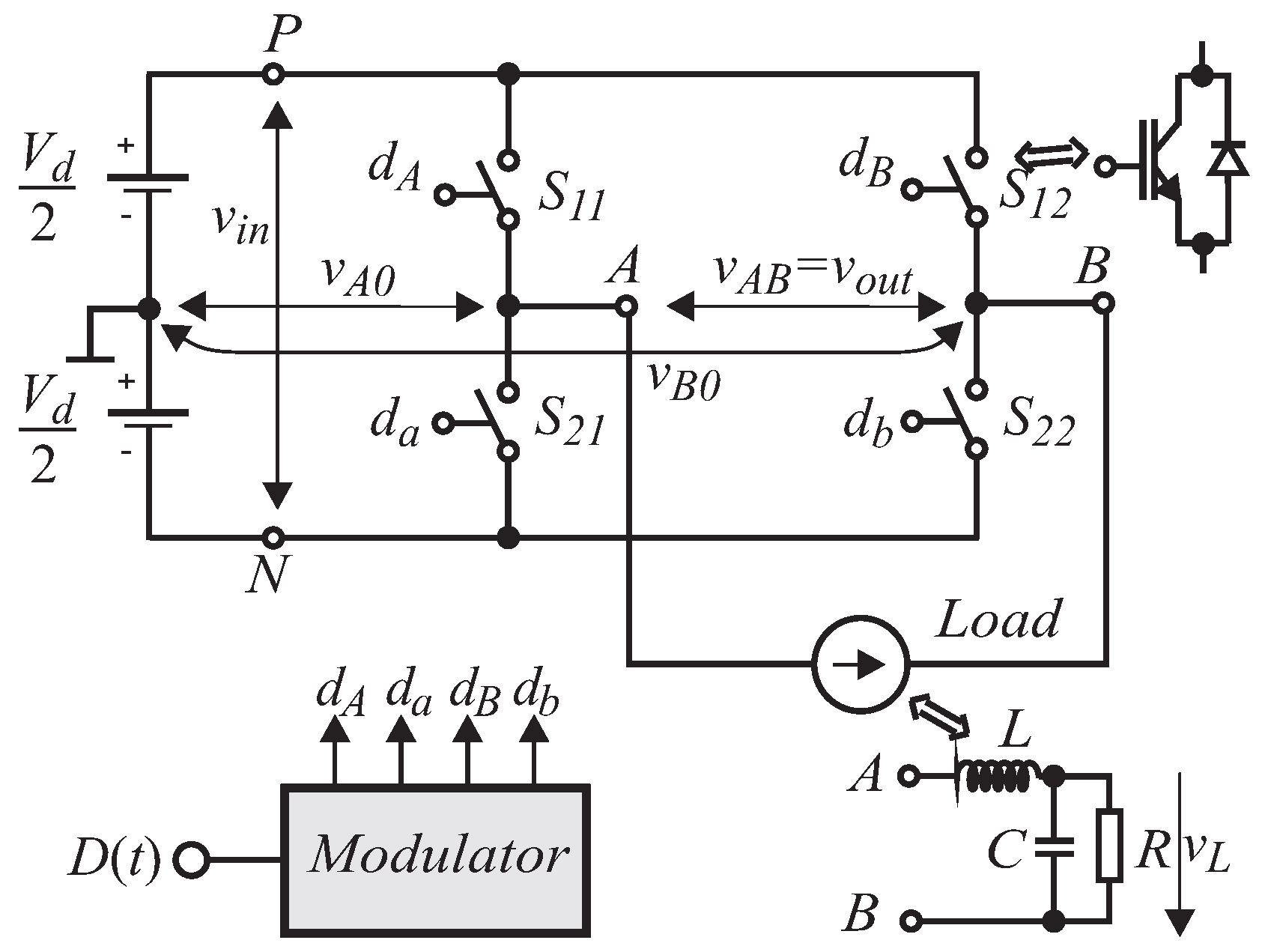
Figure 1 shows a single-phase full-bridge inverter circuit with a DC input voltage (
) and AC output voltage (
), the semiconductor switches’ structure and the load structure, respectively. The inverter consists of two legs (half-bridges) with two semiconductor switches (IGBTs or MOSFETs and diode as indicated in
Figure 1), voltage sources indicated by (
and current source (indicated by Load), representing the inverter output filter consisting of inductor
L, capacitor
C and load resistance
R. The possibility of the filter reduction by the third harmonic elimination in output voltage is considered in the next section.
The SPWM process can be divided generally into two groups with respect to the inverter output voltage
that can be either in two-level (
and
) or three-level shape (with
, 0 and
). Since it is well-known that the three-level output voltage has a better properties of spectrum, this kind of SPWM process will be considered in detail within this paper. Moreover, the first harmonic magnitude can be increased over
when over-modulation is applied, which means that the modulation index must exceed 1. By over-modulation increased magnitude of the first harmonic component is welcome in those situations where the input voltage is decreased, but additional spectrum lines appear as a consequence of this phenomenon [
10], which increases the Total Harmonic Distortion (THD) of the output signal as well.
2.1. Generation of Three-Level Output Voltage
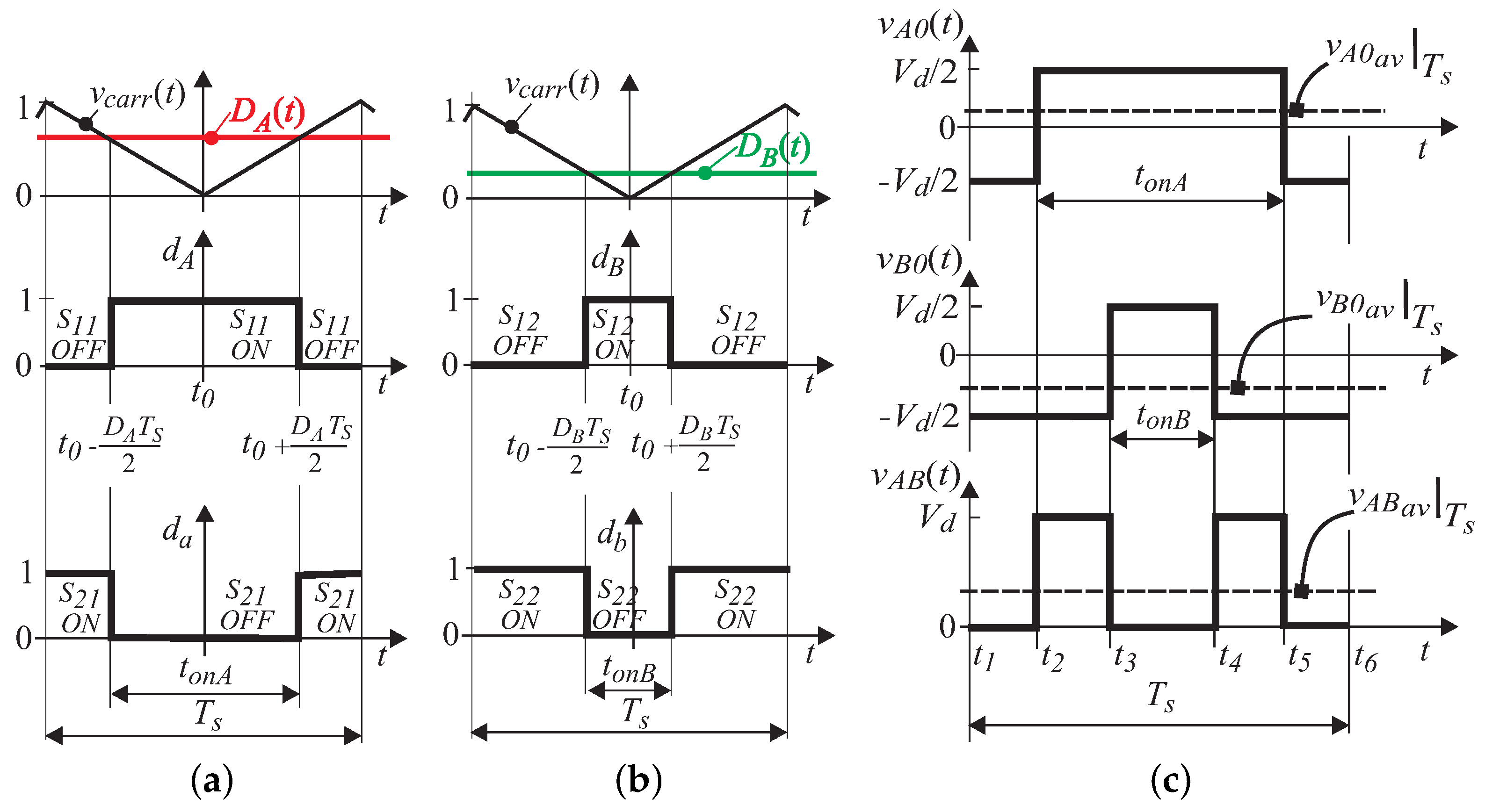
The whole inverter shown in
Figure 1 is divided into two half-bridge structures (legs). By using the first leg (switches
and
) the voltage
(“first leg” voltage) and by using the second one (switches
and
) the voltage
(“second leg” voltage) are generated at the inverter output, both with respect to the neutral point (shown in
Figure 1 and
Figure 2a, respectively). If voltage
precedes
for an appropriate phase angle the inverter output voltage
that equals the difference between voltages
and
will have the desired magnitude and desired three-level waveform, as indicated in
Figure 2a. Voltages
and
are described as two switching events:
where the switching functions (see
Figure 3a,b) are:
In order to avoid the short circuit between the battery terminals
P and
N, the following conditions must be fulfilled:
Inserting the conditions (
5) and (6) into (
1) and (2) follows to:
Referring to
Figure 3c (up and in the middle), the average value of the voltages
and
over the interval
can be evaluated as:
where
and
represent the corresponding duty cycle functions. If
holds, the following approximation can be introduced:
Functions
and
represent the desired inverter output voltages for each half-bridge, that can be expressed as:
Now, the duty cycle functions
and
can be evaluated from (
9) to (14), respectively:
where
is the modulation index. An auxiliary triangular carrier signal
needs to be introduced in order to transform the duty cycle functions
and
into switching functions
and
.
Figure 3a,b show the triangular carrier signal, and both switching functions signal, respectively. The switching functions
and
were obtained by a comparison of duty cycle functions
and
with
as follows:
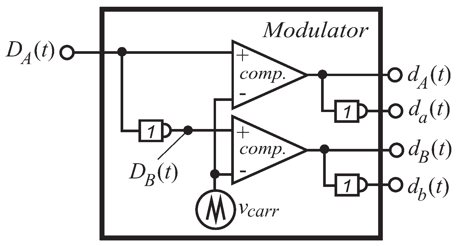
The above described procedure enables the generation of the triggering pulses in electrical (electronics) circuits for all the semiconductor switches in the inverter. When referring to
Figure 4, the comparators (
) compare the duty cycle functions
and
with triangular carrier signal (
) and the signals
and
are obtained according to (
5), (6) and (
17).
The switching signals generated according to (
17) can be considered as periodic signal on the time interval
. When they are provided to the inverter switches, the three-level voltage (as shown in
Figure 2a and
Figure 3, respectively) appears at the inverter output:
It is well-known that any periodic signal of period
can be expanded into a trigonometric Fourier series form:
where
is the frequency of the triangular carrier signal (
), and the coefficients
,
and
form a set of real numbers associated uniquely with the function
:
Each term
defines one harmonic function that occurs at integer multiples of the triangular carrier signal frequency
. According to the signal waveform of the pulse train shown in
Figure 3a, the Fourier coefficients can now be evaluated as:
In order to simplify the coefficient’s calculation, the initial time
is chosen, so the coefficient
is:
Coefficients
are also calculated from (
20):
and all coefficients
are equal to 0. According to (
19) the Fourier series of
is:
and also for the switching function
like:
2.2. The Spectrum Calculation
In order to calculate the inverter output voltage
spectrum, the same procedure can be used as follows from
Section 2.1. Voltage
can be constructed simply by subtracting outputs
and
. In practice, when the load is connected between terminals
A and
B, the voltage difference
appears on it. When (8) is subtracted from (
7) it follows to:
The switching functions
and
can be expanded by Fourier series in (24) and (25) respectively, and after applying (26) the inverter output voltage
, can be expressed by using Bessel function as described in [
7,
9,
10]:
where
. The structure of the spectral line’s appearance is evident from (27). The pulse-width modulated signal
has a fundamental component that appears at the frequency
and, besides, at the triangular carrier signal frequency
, also contains the sideband harmonics at frequencies
,
,
. Since the value of
is zero for every odd
n, the spectral lines only appear around even multiples of the carrier frequency
.
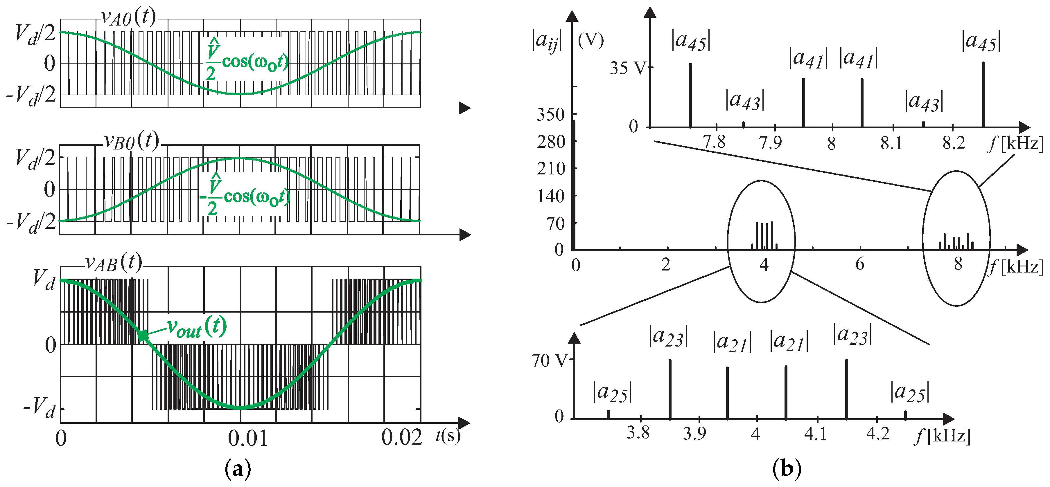
Figure 2b shows the spectrum lines for the single-phase inverter’s three-level output voltage for the
V and
, line frequency
Hz and
kHz. From all the analyses above and the obtained results, the following conclusions can be made:
The spectrum lines appear only for every even multiplier of ,
The triangular carrier signal frequency kHz is present in the half-bridge voltages ( and —not considered separately), but the synthesized inverter’s output voltage switching frequency is doubled, so the first higher harmonic component appears next to the 4 kHz, and
Filter components are needed at the inverter output in order to extract the fundamental frequency and reject the switching frequency of the output voltage and the doubled switching frequency allows reduction of the size and weight of the filter components.
3. Improved SPWM-Based Over-Modulation Strategy of Third Harmonic Elimination in a Single-Phase Inverter
Harmonic elimination [
11,
15], or looking for optimal PWM [
14], all have a long and strong tradition within the power electronics community. In a three-phase inverter it is even possible to increase the output line-to-line voltage gain by 15% by adding a specific part of third harmonic to the output of each phase [
32]. In the single-phase inverter, this measure would lead to increase of the THD. Therefore in this section, elimination only of the third harmonic component during the over-modulation regime is provided by the SPWM signal, which results in the reduced THD in the wide range of operation. The obtained lower voltage gain in over-modulation is traded off by a benefit in reduction of filter components’ size and cost.
Over-modulation appears when the duty cycle functions
and
exceeds the magnitude of the high-frequency triangular carrier signal (
).
Figure 5a shows the relationship between the triangular carrier signal and duty cycle functions
,
and their influence on the switching functions
and
, respectively. The over-modulated output voltage
can be achieved when both switching functions include the desired output voltage
and
(in
Figure 5b) like:
To eliminate the major part of the third harmonic in the single-phase output voltage, the half-bridge desired voltage
must contain the fundamental and specific negative part of the third component:
where
is the cross-section angle between the output fundamental signal and the
. Similarly, the appropriate opposite part of that component in the second inverter’s leg
can be expressed as:
The line voltages described by (30) and (31) can be expressed by Fourier series. The function is odd and, due to this, the coefficients
, so the voltages
and
are expressed only by coefficients
:
where
and the Fourier coefficients
can be evaluated from (30) and (31) by taking the symmetry of the signal during half of the period:
where
and, for the harmonic description of the output signal, it follows:
If the level of over-modulation is defined by
, the only unknown parameter here is cross-section angle
, which is, for the pure sine signal, computed initially as follows from
Figure 5b and [
10] like:
and for the modified reference signal
angle
differs slightly (see
Figure 5b) and can be calculated from the following condition (36):
or from (37) when
is replaced by the basic trigonometric triple angle formula:
The condition (37) in cubic polynomial form has three solutions for
that are difficult to write in analytical form, but can be found easily by simple numerical software packages, for example, by using the Matlab command “roots([…])”. The roots of cubic polynomial (37) are complex and real, but only the real root is used further. Once the real solution for
is obtained, the over-modulated output voltage can be evaluated from (30) and (31) as:
where the switching functions are described by Fourier series in (34), which gives:
with low-frequency spectral components in the first part and High-Frequency Spectral Components (HFSC) in the second part, where the position and magnitudes of the high-frequency spectrum lines (next to the multipliers of triangular frequency
) are described by using the Bessel series, as described briefly in the previous section, and, therefore, it will not be discussed here again. According to (34) and (39), the output voltage’s low-harmonic components can be evaluated as follows:
and allow the description of the first, third,
… and other odd spectral components (division by zero can be avoided by replacing
, where
):
Finally, from (42), it is also possible to require that the third harmonic has to be zero (
), which enables the calculation of the needed value for the compensating component (
) in the switching function as:
Starting with the initial from (35), the first value of the third component can be found by applying (45), which is then used for the correction of the angle in (37). The next value of the compensating voltage is then obtained by the new cross-section angle . After few iterations, both values ( and ) converge to the right solution, and the eliminating part of the third harmonic within the modulator can be calculated from (45) at the specific (note, that (40) describes the output voltage with- or without the compensated third harmonic component).
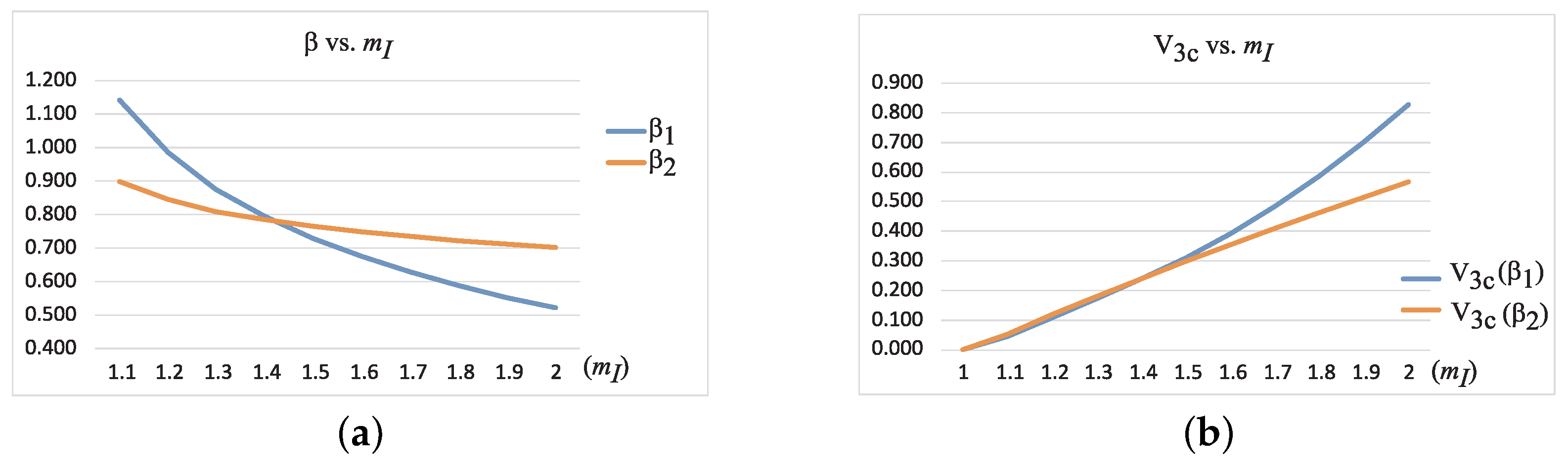
First, the influence of the angle
to the value of the compensating part in (45) for the third harmonic elimination is considered by using (35) or (37), and results are summarized in
Table 1 as
(35) and
(37). At higher over-modulation (when
is above 1.4),
is lower than the modified one
(as seen in
Figure 6a), which results in higher value of the compensating part
(shown in
Figure 6b). On the other hand, both eliminating parts
and
are almost equal for the
(see
Table 1 and
Figure 6b). A higher value of the eliminating part
is not recommended. It would result in a lower fundamental harmonic component and, consequently, higher THD, which deteriorates the quality of the inverter in general.
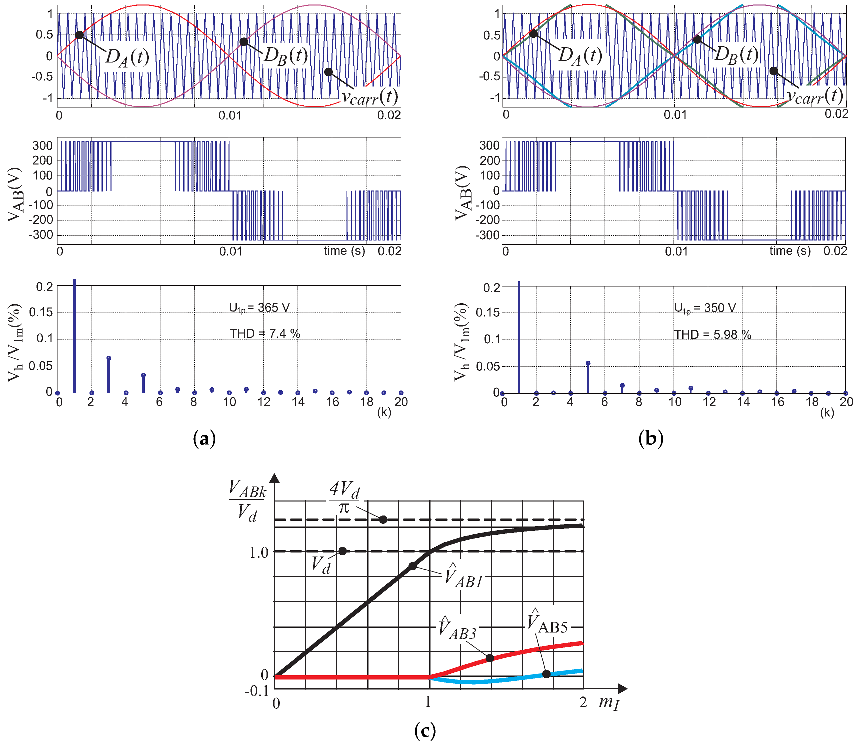
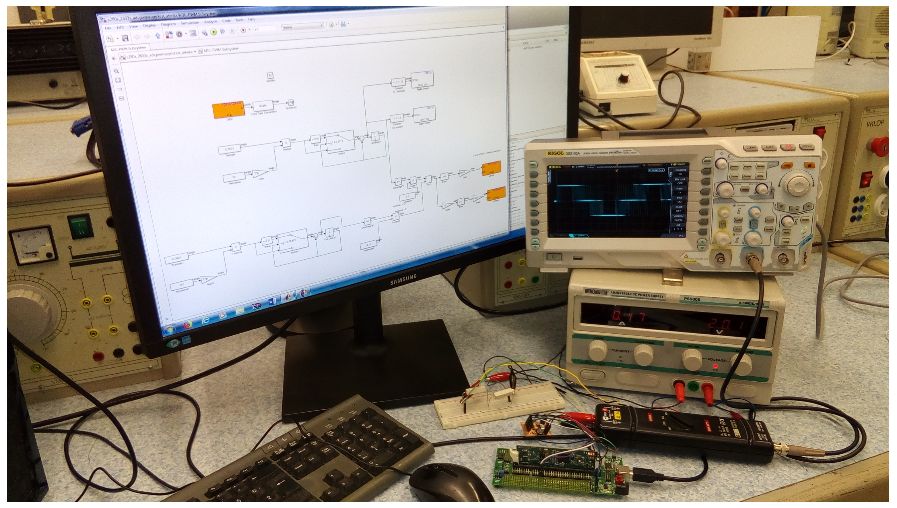
The proposed harmonic analysis was performed in the system shown in
Figure 1, and analytical results were verified by a Matlab/Simulink simulation model within the wide range of operation (
). The simulation model was built by using basic toolbox blocks (like comparators and signal generators, see block scheme in
Figure 4), and the inverter output voltage was obtained according to (38) using analytical approaches (30) and (31), while the power switches in each inverter’s leg were considered as ideal switches. The input voltage was set to
V to reach the typical rms load voltage of 230 V at the
, the fundamental frequency of the output voltage was
Hz, and the frequency of the triangular carrier signal was
kHz (the output voltage signals are shown in
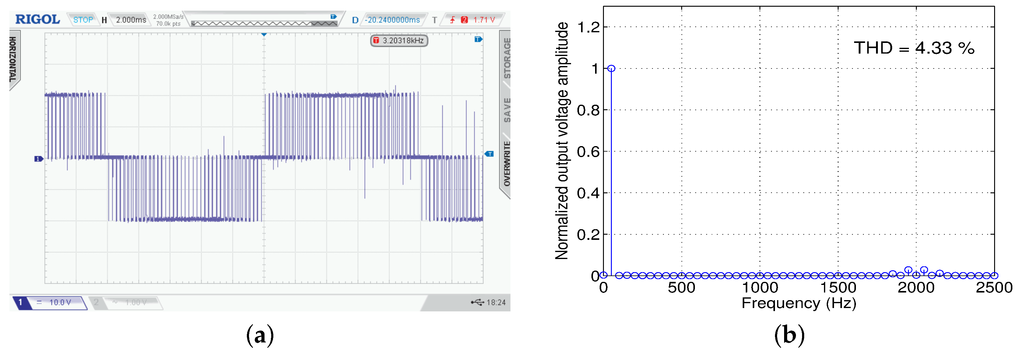
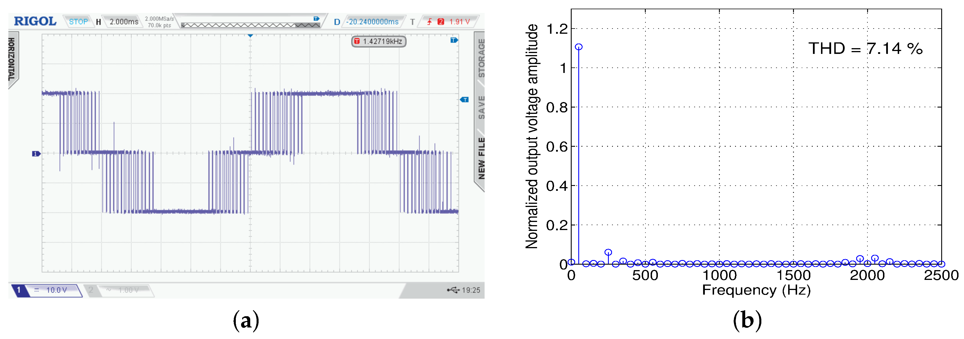
Figure 7a,b, respectively).
Figure 7c shows the first, third and fifth harmonic components versus modulation index
changing from 0 to 2, as follows from (41)–(44), and with
. As generally follows from (40), the magnitudes of harmonic components start to increase when
exceeds 1. For the case of
, the obtained results are summarized in
Table 2. Apparently the magnitude of the first harmonic exceeds the DC-link voltage
by 10.6%, and the magnitude of the third harmonic is cca. 6% of
with SPWM without compensation. When the proposed improved SPWM method is applied, the first harmonic exceeds the DC-link voltage
by 6.1% and the third harmonic is almost completely eliminated. The upper limit of the first harmonic in the improved SPWM method is obtained from (41) when the modulation index is high and, according to
Figure 5b, the cross-section angle
, which leads the first voltage harmonic toward the
(the same is true for the square signal). In
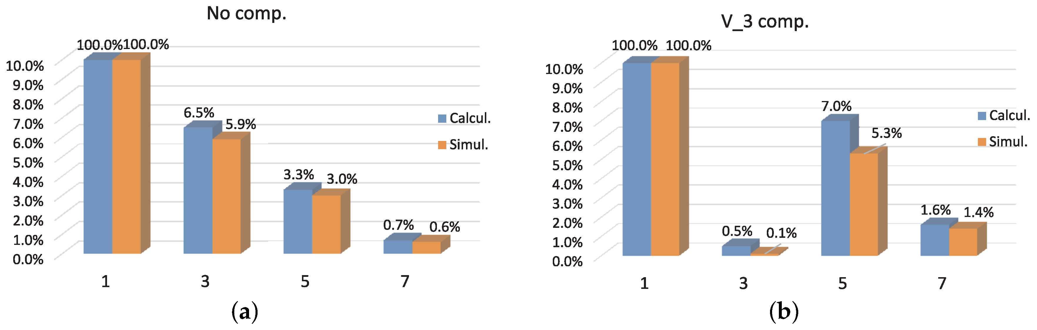
Table 2, each harmonic component is calculated numerically and compared with the simulation model without and with the third harmonic elimination, and differences are summarized in
Figure 8. As predicted by the proposed method, the third harmonic has been almost eliminated. On the other hand, there is a slight increase in the fifth and seventh harmonics, but there is still a promising reduction in THD of about 1.4% (see
Figure 7a,b), or even more at a higher over-modulation rate (
Figure 9b). Once the maximum allowed THD is defined, it is possible to set the belonging
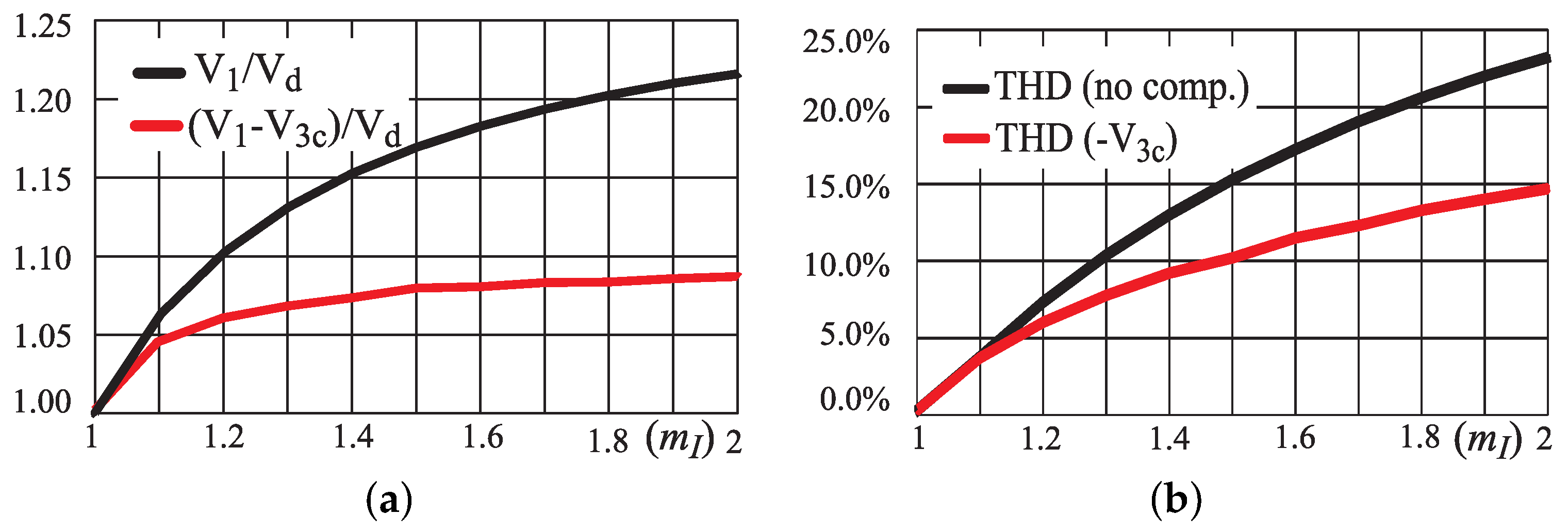
in the over-modulation working regime and increase the output voltage in the case of losing the DC-link voltage. When considering the grid regulative requirements, the rest of the high order harmonics can be attenuated more easily by using smaller and cheaper filter components.
Limitations of the Improved SPWM Over-Modulation Strategy
The price for effective harmonic elimination and THD reduction at the same time is reduction of the voltage gain at higher over-modulation rate (see
Figure 9a), so the improved SPWM strategy assures good performance up to modulation index
. However, the fact is that the single-phase inverter systems without built-in harmonic elimination would have higher THD at the same modulation index as well (as shown in
Figure 9b), which actually makes the proposed strategy superior. When the strategy was tested for the elimination of two (third and fifth) harmonic components, the increase of the first harmonic magnitude was negligible, so the improved SPWM strategy is limited to eliminating only one harmonic component effectively. A low THD of inverter output voltage can be obtained with the improved SPWM strategy, similarly to the standard SPWM, when the ratio between the switching frequency
and the fundamental frequency
is large enough (
), which influences the inverter efficiency.


