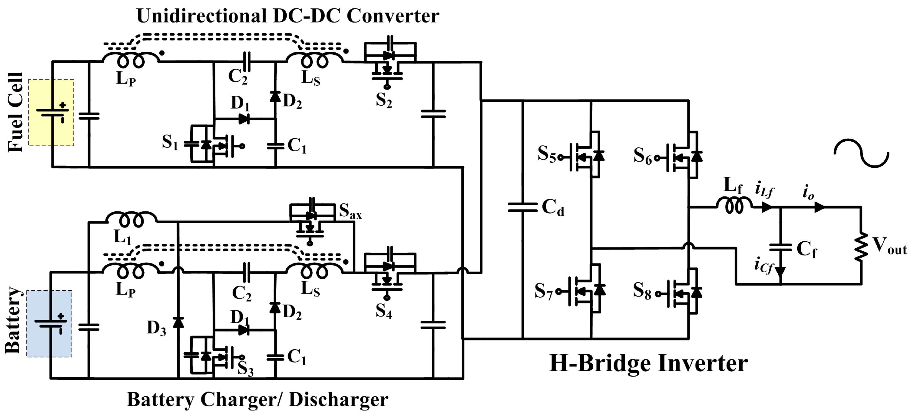
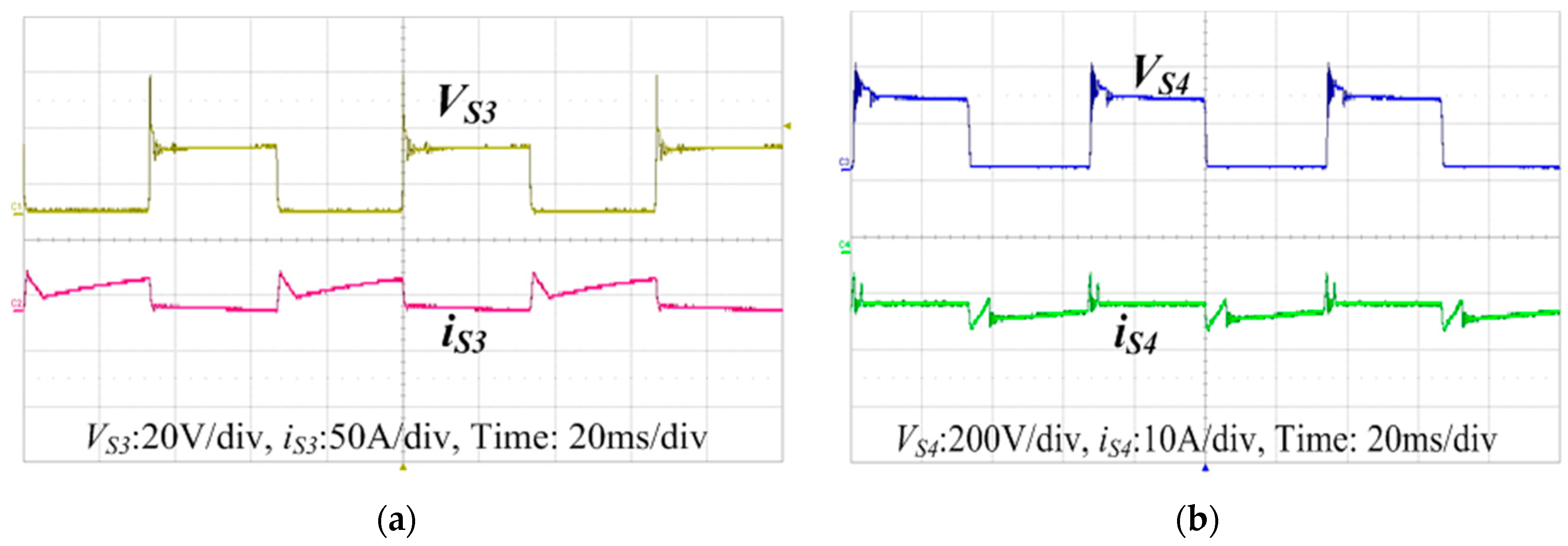
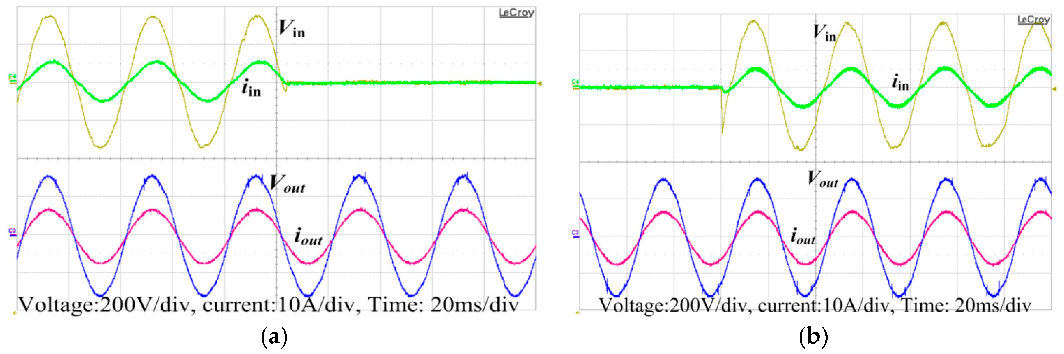
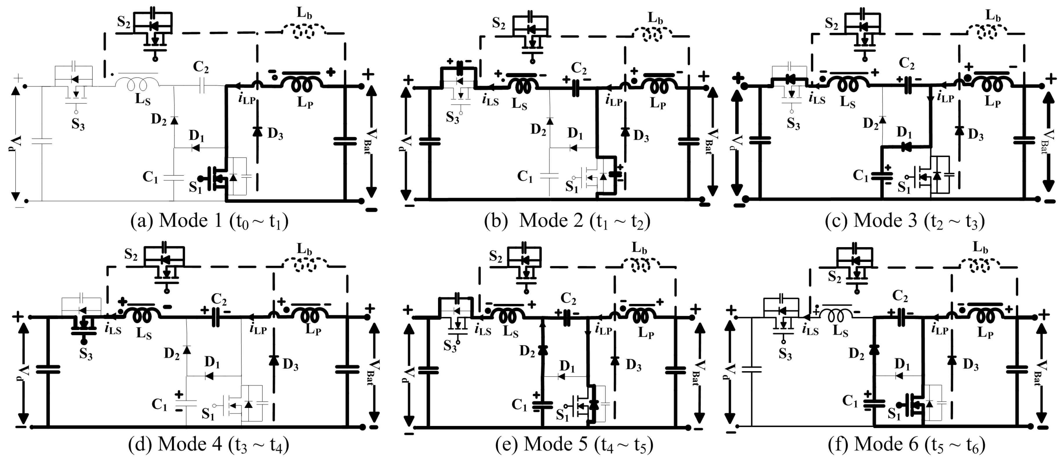
3.1. Inverter Control
For our proposed UPS topology, a cascaded control algorithm using Slide Mode Control (SMC) and Proportional Resonant (PR) control has been considered to control the inverter output voltage. The slide mode control is used in current loop while the PR control is used in the voltage loop. The chattering phenomenon corresponding to the slide mode control is prevented by utilizing the law of smoothed control in narrow boundary layer. This law, when implemented on the pulse width modulator leads to the inverter operation with a constant switching frequency. Hence, our proposed controller consists of the properties of both the PR control as well as the SMC control. The employed controller exhibits great response with low THD and also shows high stability for non-linear loads.
The schematic diagram of single phase inverter consisting of an LC filter and our proposed controller for non-linear load condition is depicted in
Figure 1. V
d indicates the applied DC link voltage, V
out is the output voltage of the filter capacitor C
f.
iLf is the current in the inductor L
f and
iO represents the output current through the load R, equivalent to
iO = V
out/R. The state equations representing the inverter are given as
where
.
In order to implement the SMC, the voltage error x
1, and its derivative
need to be found as:
where
Consider the slide surface equation
where
S denotes the sliding surface. The sliding function must be stabilized. To ensure this, the Lyapunov function V(t) = S
2/2 needs to be satisfied with the minimum condition
, maintaining the scalar
at 0 while
is stringently kept as a positive constant. Consequently, the stability condition will be
.
To ensure the satisfaction of the sliding condition (30), despite the uncertainty regarding the non-linear function dynamics, u is replaced by the following function.
Therefore, it can be seen that the stability condition would be fulfilled if Equation (36) is satisfied. Now, in order to apply the law of sliding control to the inverter, inputting the values of x
1 and x
2:
As the sliding mode controller inherently possesses the chattering property, it is accompanied by lower control accuracy and high losses in the circuit. Smoothed slide mode control has been implemented to get rid of this inherent chattering phenomenon. This is done by smoothing the control discontinuity in a thin boundary layer neighboring the sliding surface.
where
. is the thickness of the boundary layer and
. is the width of the boundary layer. Therefore,
. is chosen in such a way that all the trajectories beginning at
stay inside
for all t > 0. Hence, we interpolate S inside
, for instance, and replace S by the expression S/
. Thus, Equation (38) will become
The smoothing control employs a low pass filter to the local dynamics, thereby eliminating the chattering phenomenon. As stated before, this technique, when applied to the pulse width modulator, also results in a fixed switching frequency operation of the inverter. The control law is required to be tuned extremely precisely so as to obtain a balance between precise tracking and robustness to the uncontrolled dynamics.
The PR controller normally provides a large gain at the fundamental frequency while strictly following the reference sinusoidal signal, decreasing the steady state error, and enhancing the system stability. The ideal PR controller transfer function is given by Equation (41):
where K
P is the proportional gain, ω
0 represents the resonant frequency, and K
R is the resonant gain.
The ideal PR controller provides an infinity gain at the resonant frequency while providing no gain and phase shift at frequencies other than the resonant frequency. Hence, a more appropriate control is a non-ideal PR control, given by Equation (42):
Thus, selecting an appropriate cutoff frequency ωc can make the bandwidth wide and can reduce the sensitivity towards variations in frequency. By using a combination of the PR controller and slide mode control, the performance of the inverter is significantly improved, as the resonance controller provides a better output voltage regulation and can cause a considerable reduction in the net harmonic distortion.
Thus, we can serve the final equation for the inverter control by combining the proportional resonant control and slide mode control for the current loop.
Hence, Equation (43) indicates the dynamic behavior of the inverter utilizing both PR compensator as well as SMC. As the error current in the capacitor consists of the ripples from the inductor, the current peak may achieve high values. So the value must be assigned with great care so as to compensate the slope from the high current ripple corresponding to the capacitor. Thus, the PR controller removes the steady-state error at the resonant frequency or any harmonic at that frequency.
The robustness of the system and its dynamics are determined by , which represents the response time of the system. It can be seen in Equation (43) that a smaller value of leads to a slowly responding system, while higher values of would increase the response time but the system would take much longer to reach the sliding surface. Hence, the optimal value is equal to the inverter switching frequency.
According to [
22], the carrier wave slope is represented by
, where
is the magnitude of the carrier wave and
fs is its frequency. The error signal slope to the modulator is given by the expression
. The limitation of the pulse width modulator implies that the slope of the error signal must be smaller than the slope of the carrier signal, i.e.
Error signal slope < Carrier signal slope
Hence, the minimum
value can be computed using Equation (45):
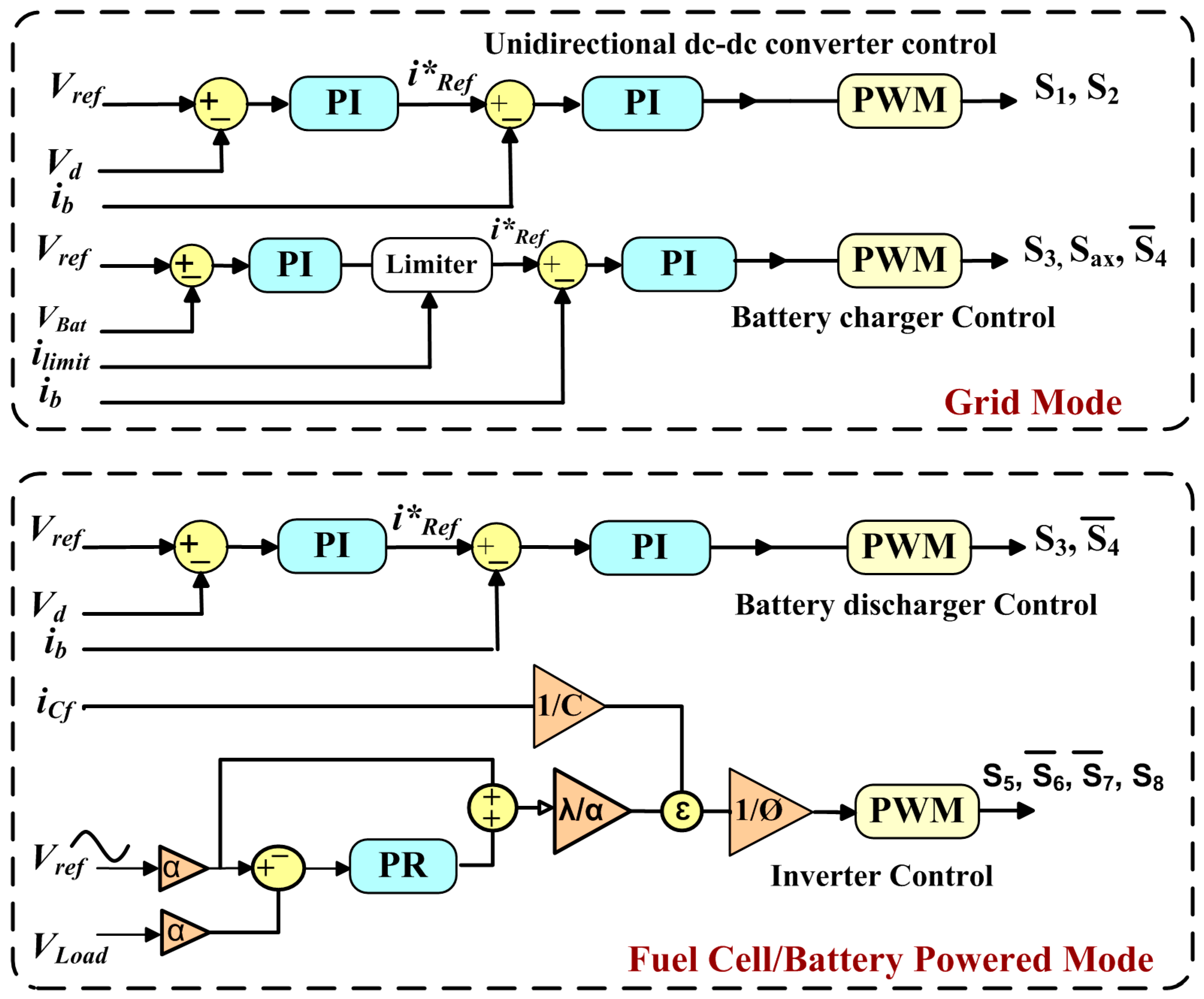
For designing a controller for an inverter, as depicted in
Figure 9, the value of
can be derived using Equation (45) by taking into consideration the circuit parameters given in
Table 4. K
P and K
R represent the proportional gain and resonant gain that are selected to obtain a stable response of the PR controller. α represents the division factor that is required to make the output voltage comparable to the reference voltage and is selected by considering the limitations of the electronic circuitry. λ represents the inverter dynamic response and equals the switching frequency of the modulator. Carrier magnitude (V
m) is selected in order to realize the inequality given in Equation (44). The final control parameters derived, ensuring the stable inverter operation, are presented in
Table 4.

 ,
, 


