Article

A Novel Concept for Three-Phase Cascaded Multilevel Inverter Topologies

Department of Electrical and Computer Engineering, Curtin University, Perth, WA 6102, Australia
*
Author to whom correspondence should be addressed.
Energies 2018, 11(2), 268; https://doi.org/10.3390/en11020268
Submission received: 16 November 2017 / Revised: 3 January 2018 / Accepted: 15 January 2018 / Published: 23 January 2018
(This article belongs to the Section F: Electrical Engineering)

Abstract

:
One of the key challenges in multilevel inverters (MLIs) design is to reduce the number of components used in the implementation while maximising the number of output voltage levels. This paper proposes a new concept that facilitates a device count reduction technique of existing cascaded MLIs. Moreover, the proposed concept can be utilised to extend existing single phase cascaded MLI topologies to three-phase structure without tripling the number of semiconductor components and input dc-supplies as per the current practice. The new generalized concept involves two stages; namely, cascaded stage and phase generator stage. The phase generator stage is a combination of a conventional three-phase two level inverter and three bi-directional switches while the cascaded stage can employ any existing cascaded topology. A laboratory prototype model is built and extensive experimental analyses are conducted to validate the feasibility of the proposed cascaded MLI concept.

1. Introduction

Multilevel inverters (MLIs) have drawn much attention in renewable, vehicular and industrial applications [1,2,3,4,5,6]. Also, MLIs have been utilized in flexible AC transmission, heating and air conditions [7]. Conventional MLIs include diode clamped or neutral point clamped (NPC), flying capacitor (FC) and cascaded H-bridge (CHB) MLI. Among these types, CHB MLI has been found very reliable in high voltage/high power applications (6.6–13.8 kV, 500 MVA) [8,9]. Several research efforts have been conducted to reduce the number and complexity of DC voltage supplies management [10,11].
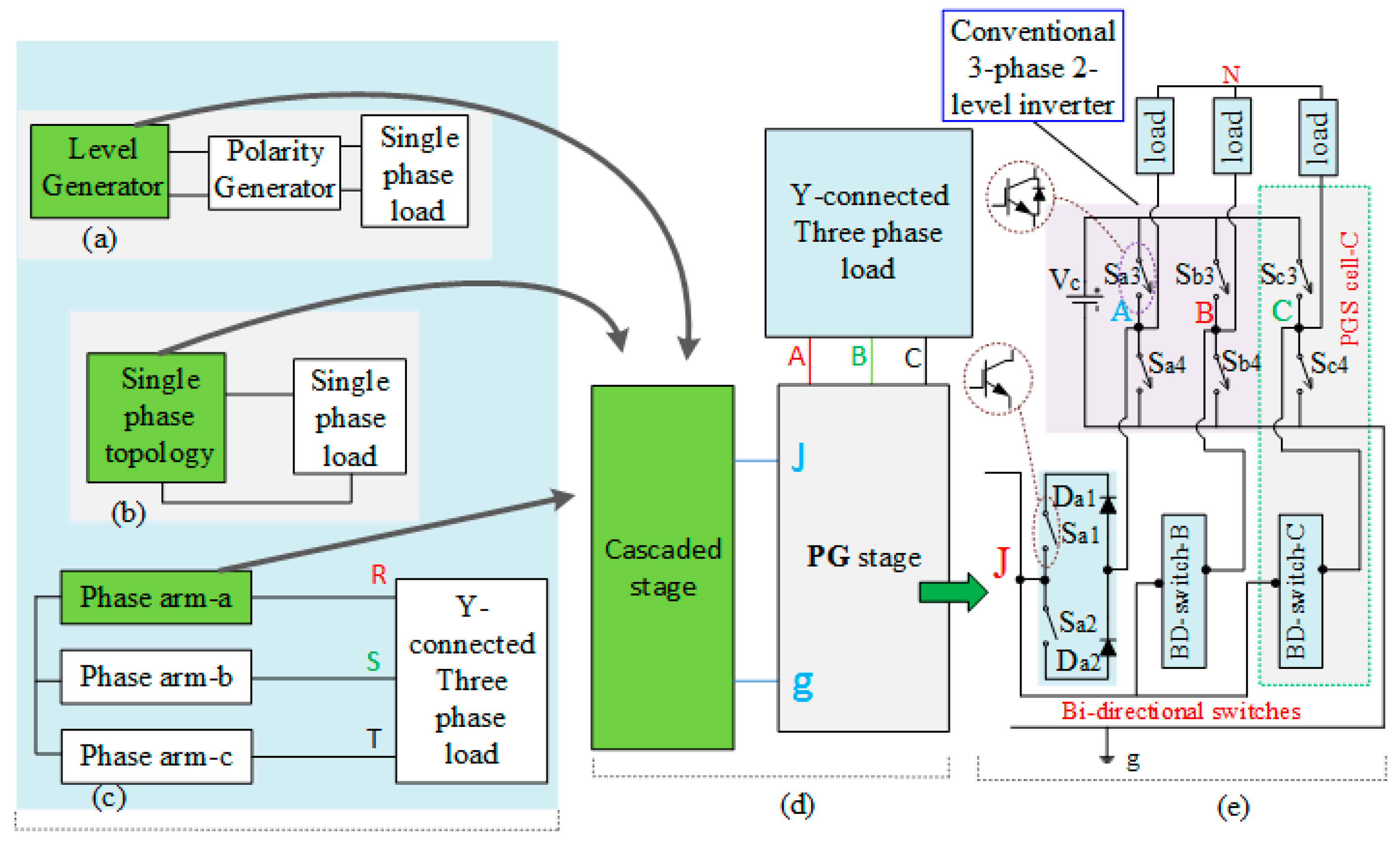
Extensive research can be found in the literature to reduce the device count of cascaded MLI (CMLI). Several cascaded MLI topologies comprise two main parts; level generator and polarity generator as shown in Figure 1a can be found in the literature [12,13,14,15]. The level generator is a cascaded connection of a number of inverter cells that generates multilevel unipolar voltage while the polarity generator converts this unipolar voltage into bipolar voltage waveform [13]. While level generator structure varies for different topologies, the structure of polarity generator has been always an H-bridge connection involving four semiconductor switches. The number of cascaded cells in the level generator may be increased and/or asymmetric input voltage sources can be used to enhance the number of levels in the output voltage waveform without any change to the polarity generator [12]. The level generator switches may work with high frequency, but the polarity generator switches always function at line voltage frequency [13].
Other CMLI topologies which are able to generate bipolar voltage without using polarity generator as shown in Figure 1b were proposed in the literature [16]. CMLI topologies such as cross-switched and modified H-bridge topologies were also recently proposed in the literature [17,18,19,20,21,22,23]. Among the above mentioned CMLI topologies, some were mainly developed for three-phase multilevel voltage generation and cannot be directly utilized for single phase applications e.g., Figure 1c [24,25].
Three-phase CMLI has been widely used in large-scale renewable energy applications to comply with the high-power conversion requirement [1,2,3,4]. In order to improve the quality of the output voltage waveform, the number of components required to implement the three-phase CMLI should be significantly increased which increases the implementation cost, inverter physical size and complicates the control system. Although several topologies have been proposed in the literature in order to reduce the device count and increase the number of levels in the output voltage of single phase CMLIs, the majority of these topologies have not been extended to three-phase structure yet. It is a common trend that the number of components of single phase topologies is tripled when they are extended to three-phase structures [13,14,26,27,28].
Both high frequency and low frequency modulation techniques have been reported as reliable control strategies for CHB MLI [29,30]. The most common high frequency modulation strategy is carrier-based sine pulse width modulation (SPWM) strategy and a wide range of carrier frequency (1–12 kHz) is employed to get the switching pulses [27,28,31,32]. The main problem of SPWM strategy is that it has severe consequences on switching losses [33]. On the other hand, low frequency modulation strategies provide better output voltage waveform with low total harmonic distortions (THD) [25,34].
The main goal of this paper is to introduce a new generalized CMLI topology that could be employed to extend any existing single-phase CMLI topology to a three-phase structure without tripling the devices used within the single-phase structure. The proposed topology can also be employed by existing three-phase CMLI topologies to reduce its device count without compromising its performance. Besides, a low frequency space vector modulation (SVM) technique is applied to generate switching pulses. The proposed topology provides an optimized design solution to CMLI in terms of reducing the implementation cost and physical size while maintaining the quality of the output voltage waveform.

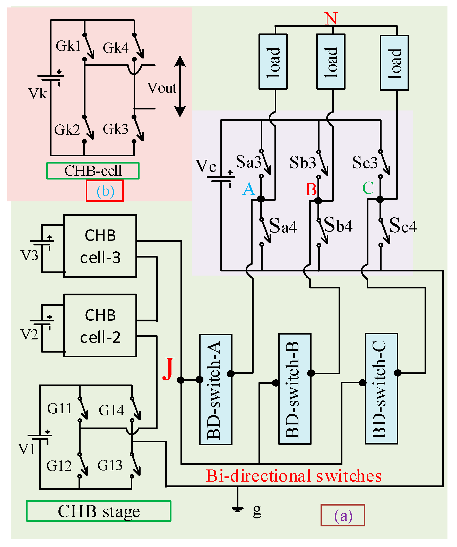
2. Proposed Concept of 3-Phase CMLI

Figure 1d shows the block diagram of the proposed three-phase CMLI, in which a cascaded stage is connected with the polarity generator (PG) stage at junction point ‘J’. The structure of the cascaded stage is not fixed as it can be replaced by any existing cascaded MLI topology. The green shaded portions of existing CMLI topologies in Figure 1a–c can be employed as a cascaded stage in the new proposed topology. The PG stage is developed by utilizing three Bi-directional (BD) switches and a conventional three-phase two level inverter (CTPTLI). Each BD switch consists of two insulated gate bipolar transistors (IGBT) and two diodes. Both IGBT switches work simultaneously to turn the BD on or off. Three-phase arms A, B, and C exist in the PG stage. A BD switch and two switches in the CTPTLI can be considered as a PG cell in each phase arm with 120° phase difference among the switching devices of the three cells. The CTPTLI is fed by a dc-voltage supply ‘VC’ of a magnitude greater than the summation of the input voltage supplies in the cascaded stage.
Each pair of the switches, (Sa3, Sa4), or (Sb3, Sb4), or (Sc3, Sc4) within the CTPTLI at different PG cells are responsible for generating VC and zero voltage levels in the output voltage waveform at the output nodes A, B, C. For any PG cell, the PD-switch is turned off while the two switches within the CTPTLI operate to generate VC and zero voltage level. The pair switches in the CTPTLI and the BD switch always function in a toggle mode. As mentioned above, any existing CMLI topology can be utilized as a cascaded stage and, hence, no significant change is required in the switching logic for existing CMLI topology when used as a cascaded stage to generate different voltage levels in the proposed topology.
In any PG cell, the PD-switch is only turned on for conducting the voltage levels, which are generated by the cascaded stage to the output points A, B, C. Three BD-switches, which are connected with the cascaded stage at the junction point ‘J’ as shown in Figure 1e are operated with a 120° phase difference. Figure 2a shows the simplified structure of the PG stage for generating the voltage levels VC and 0 in the pole voltage VAg which are achieved by toggle operation of switches Sa3 and Sa4. Figure 2b shows the conduction path of the inverter when it generates intermediate levels between VC and 0 in the pole voltage. Figure 2c shows the final pole voltage.
If VAg, VBg, VCg are the pole voltages, then the line voltage, VAB, VBC, VCA can be derived as below,
[ V AB V BC V CA ] = [ 1 1 0 0 1 1 1 0 1 ] [ V Ag V Bg V Cg ]

3. Proposed CMLI Using H-Bridge Topology as Cascaded Stage

Cascaded H-Bridge (CHB) MLI topology is a well-established structure for single and three-phase applications [35]. The cascaded stage in the proposed generalized CMLI is facilitated to utilize any single- or three-phase structure as shown in Figure 1.
The conventional CHB MLI topology shown in Figure 3 for n-number of CHB cells is chosen to validate the proposed three-phase inverter concept. The proposed three-phase MLI structure involving three CHB cells in the cascaded stage is shown in Figure 4a.
The number of CHB cells in the cascaded stage can be increased in order to achieve more levels in the output voltage waveform. Each H-bridge cell (k) comprises four switches (Gk1, Gk2, Gk3, Gk4) and a dc-power supply (Vk) as depicted in Figure 4b. Any CHB cell is able to produce three different voltage levels (Vk, 0, −Vk) in the output voltage, Vout. Table A1 in the Appendix A shows the switching logic to achieve the aforementioned three output voltages.
Symmetric and asymmetric structures are proposed for conventional CHB MLI topology in [35,36], respectively. Asymmetric methods are found superior than the symmetric in terms of the number of levels in the output voltage as presented in [35]. In [37], an asymmetric CHB MLI is presented, where the dc voltage ratios are kept in binary form (1:2 … 2n). The Trinary ratio format (1:3: … :3n) has been also proposed for CHB MLI asymmetric structure [38]. The new proposed three-phase CMLI concept in this paper can adopt both symmetric and asymmetric structure of the CHB MLI in the cascaded stage.
As mentioned above, the magnitude of the VC should be greater than the summation of the connected voltage supplies in the cascaded stage. If V1, V2, …, V3 are the input voltages for n-number of cells in the cascaded stage, then the following respective equations for symmetric, binary-related and trinary-related input supplies can be written,
V 1 = v ;     V 2 = v ; ;   V n = v
V 1 = v ;     V 2 = 2 1 v ; ; V n = 2 n 1 v
V 1 = v ;     V 2 = 3 1 v ; ;   V n = 3 n 1 v
where ‘v’ is the per unit voltage value.
The input voltage-supply of the CTPTLI, VC can be calculated from,
V C = 0 n V x + V 1 = ( V 1 + V 2 + + V n ) + v
Figure 5 shows the conduction path for generating the pole voltage. In Figure 5, the magnitudes of the CHB cells input voltage supplies are considered symmetric i.e., V1 = V2 = V3 = v; VC = 4v. With the contribution of CTPTLI and CHB cells along with the BD-switches, pole voltages, VAg, VBg, VCg are produced. Only the CTPTLI switches operate to generate the voltage levels, VC and 0 as shown in Figure 5a,e, respectively. The other voltage levels, (V1 + V2 + V3), (V1 + V2), V1 between 0 and VC levels are produced using different switching logics among the CHB cells, when the BD-switches are turned on. Figure 5e shows the pole voltage output, VAg, which can be obtained by the above mentioned switching operation.
While Figure 5 explains the generation of one arm pole voltage, VAg; the other two pole voltages follow the same switching logics with 120° phase shift among the PG-cells. The switching function for each phase arm lasts for 120° phase angle.

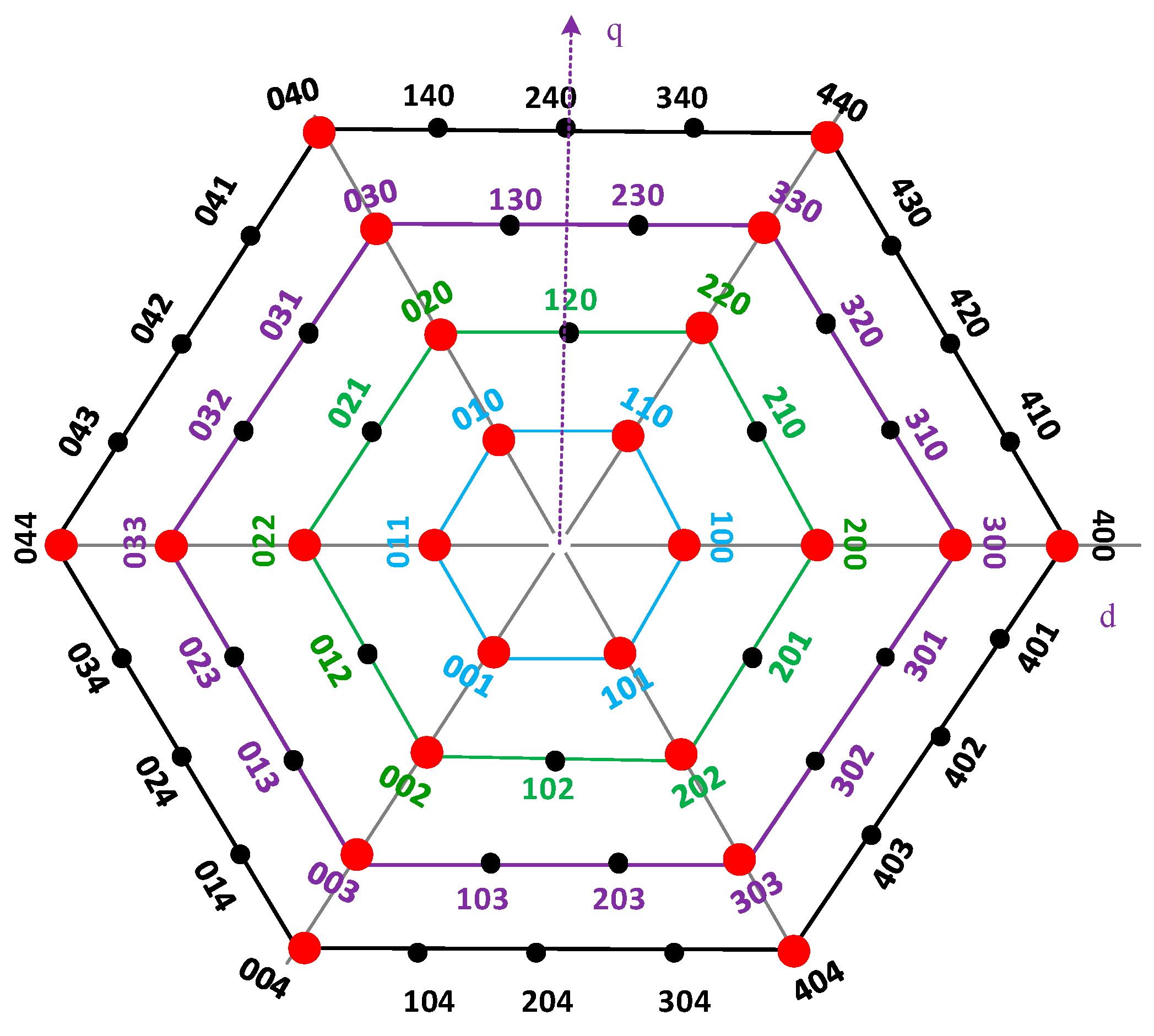
4. Implementation of the Proposed MLI

The proposed MLI topology in Figure 4 is controlled with a low frequency staircase modulation strategy [39,40]. The switching states follow a specific sequence in the d-q plane. The number of switching states, S in the d-q plane is an essential factor to generate the output voltage levels and can be expressed as,
S = 6 ( N P 1 ) ; N P > 1
where NP is the number of levels in the pole voltages.
The number of switching states forms different hexagons as shown in Figure 6 to achieve different number of levels in the pole voltage waveforms.
In Figure 6, the smallest hexagon represents the switching states for NP = 2 and the following hexagons is for NP = 3, NP = 4, and NP = 5; respectively. According to Figure 5, the proposed topology generates NP = 5 in the pole voltages. Hence, the most upper hexagon in Figure 6 is appropriate for getting 24 switching states to generate five voltage levels, 4v, 3v, 2v, v, 0 in the pole voltages.
The 24 switching states are, 044, 043, 042, 041, 040, 140, 240, 340, 400, 430, 420, 410, 400, 401, 402, 403, 404, 304, 204, 104, 004, 014, 024, 034. Each of the switching states has three switching vectors, Sa, Sb, Sc for three-phase voltage generation. The pole voltages, VAg, VBg, VCg are taken as reference to achieve the three switching vectors in each switching state at any instant of time [39]. In general, the switching angles, φ for each of the switching states are equal and can be calculated from,
φ = 360°/S
Hence, the switching angle of each of the 24 switching state is 15°. This means, a new switching state will come into operation every 15°. In the switching sequence of 24 switching states, the switching vectors 4, 3, 2, 1, 0 are combined in an organised manner to generate three pole voltages and the switching vectors always abide by Table A2 in the Appendix A for different voltage level generation.
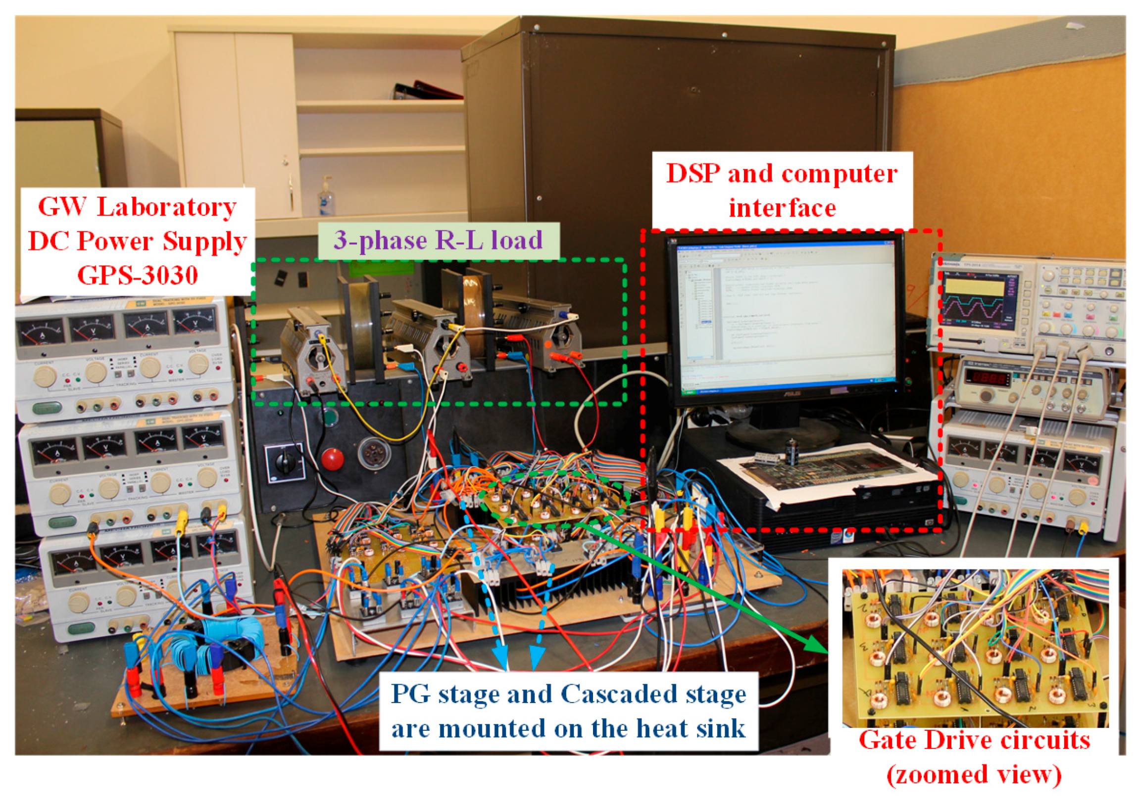
The real time switching signals are obtained using digital signal processor, TMS320F2812 (Texas Instruments, Dallas, TX, USA). The implementation requires 12 IGBTs for three CHB cells in the cascaded stage and 12 IGBTs in the PG cells. A laboratory prototype is developed to validate the feasibility of the proposed inverter.
Figure 7 shows the developed hardware prototype model. A total of 21 general-purpose input/output (GPIO) pins are required in the DSP, TMS320F2812 for achieving all real-time switching signals. Sixteen (GPIOA0-GPIOA15) pins are chosen from GPIO-A while the remaining one pin is chosen from GPIO-B (GPIO B0) pin array. The gate signals of phase B and C within the three PG-cells have similar pattern as in phase-A with a phase shift of 120° and 240°, respectively.
Six IGBTs, IRG4BC40W, 600 V/20 A along with six diodes, RHRP1540, 400 V/15 A are used for the three BD-switches in the PG-stage while 18 IGBTs, HGTG20N60B3D, 600 V/40 A are used to build the CHB cells in the cascaded stage and CTPTLI. A four channel digital storage oscilloscope, Tektronix TPS 2014 (Tektronix Inc., Beaverton, OR, USA) is utilized to capture the experimental output waveforms and analyse total harmonic distortion (THD).

5. Results and Discussions

Table A3 in the Appendix A shows system specification of the implemented inverter. To validate the feasibility of the proposed topology, its performance in terms of output voltage/current waveforms along with the THD has been compared with the performance of the MLI topology presented in [5,40]. As will be elaborated below, while the proposed topology in this paper can reduce the MLI device count significantly, it almost provides the same performance of the MLI topology presented in [5,40]. Results in various test cases are demonstrated in the following sub-sections.
A. H-bridge cells symmetric input supplies
The input dc-voltage sources are connected such as V1 = V2 = V3 = v = 70 V and VC = 4v = 280 V. Inductive 3-phase load (Z = 55 + j 37.68 Ω/phase) is considered for testing the inverter performance.
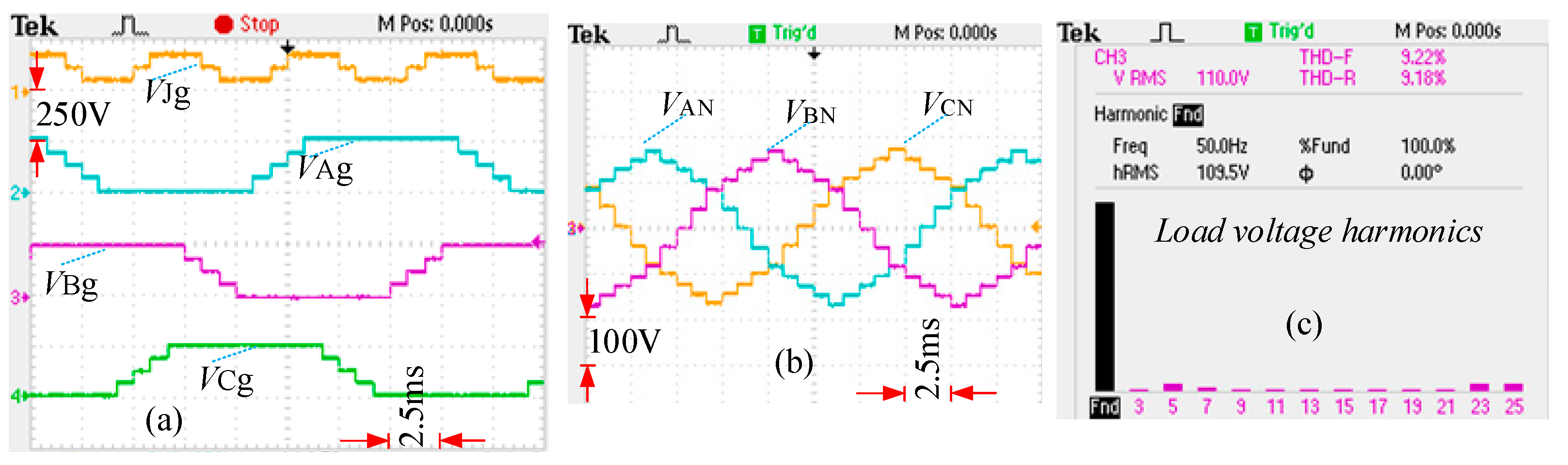
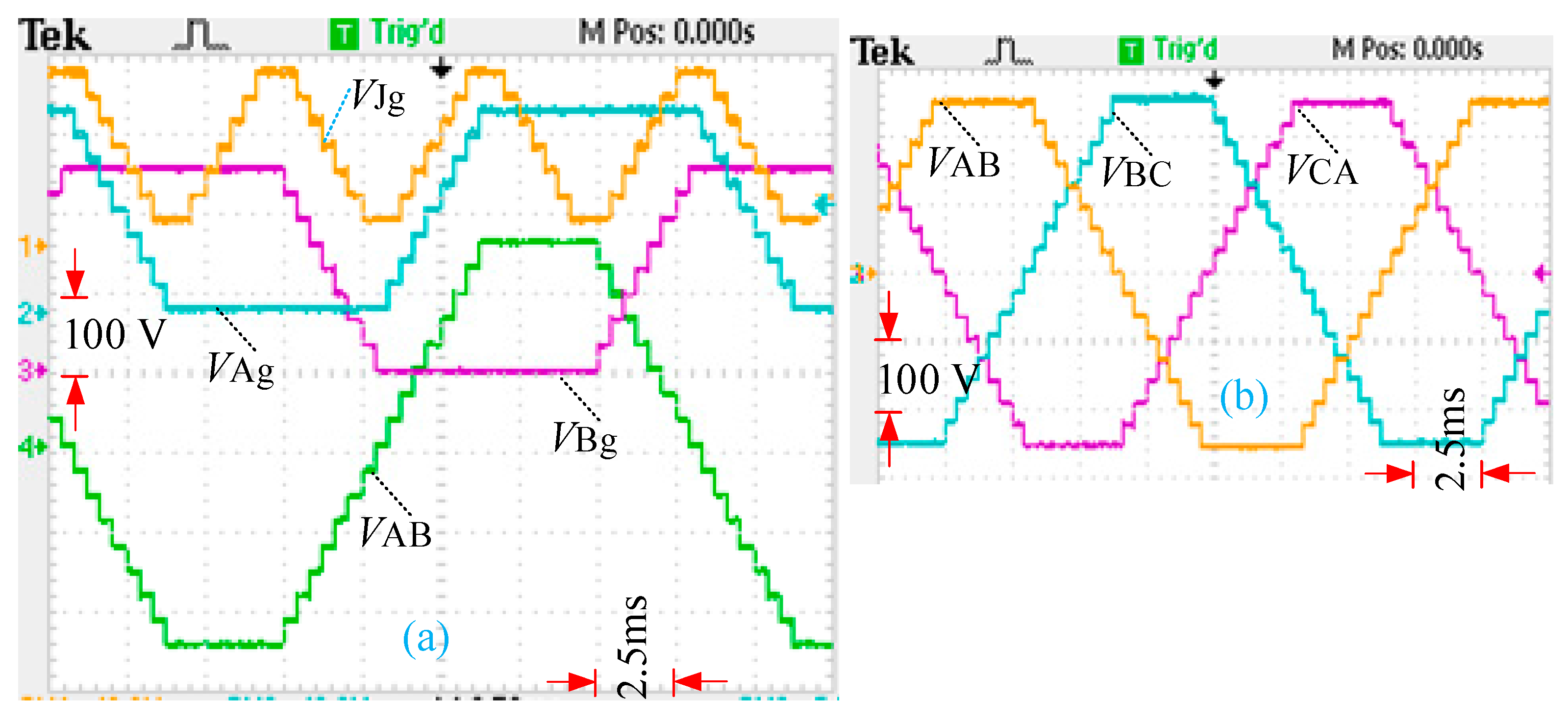
Figure 8a shows the junction voltage, VJg and pole voltages, VAg, VBg, VCg, respectively. As shown in the figure, the pole voltages comprise five levels (280 V, 210 V, 140 V, 70 V, 0) while VJg comprises three levels (210 V, 140 V, 70 V). Figure 8b,c show the load voltages, VAN, VBN, VCN, and their THD, respectively. The relation between the pole voltages VAg, VBg, VCg, and load voltages can be expressed by,
[ V AN V BN V CN ] = 1 3 [ 2 1 1 1 2 1 1 1 2 ] [ V Ag V Bg V Cg ]
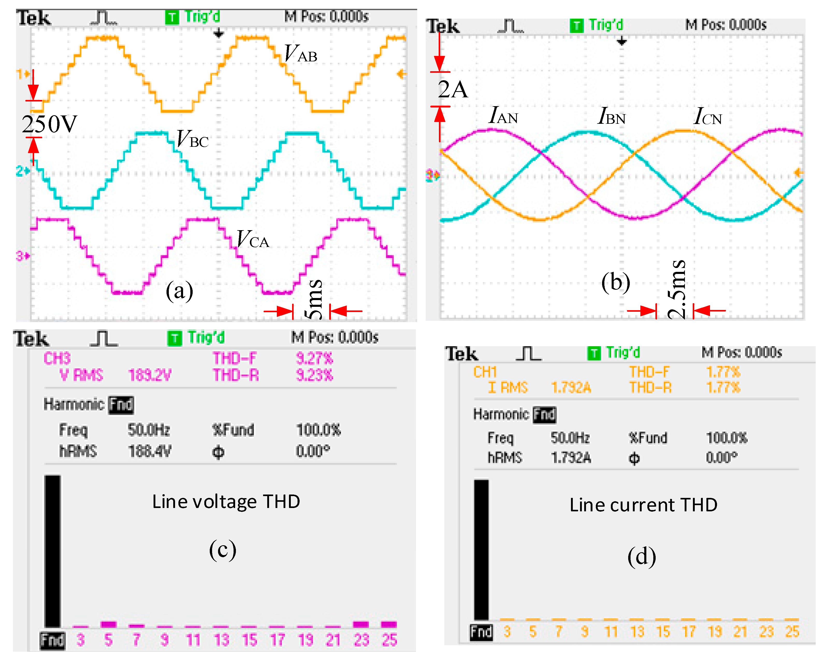
On the other hand, the line voltages, VAB, VBC, VCA shown in Figure 9a comprise nine levels (280 V, 210 V, 140 V, 70 V, 0 V, −70 V, −140 V, −210 V, −280 V).
Figure 9b shows the three-phase line currents, IAN, IBN, ICN. It is worth mentioning that no harmonic filter was used in the implemented hardware setup. The total harmonic distortion (THD) of the unfiltered line voltage and line current are 9.27% and 2.09%; respectively as shown in Figure 9c,d, respectively. The THD of the line current and voltage must be less than 5%, to comply with the IEEE standard [41]. While the current THD complies with the mentioned standard, voltage THD is more than 5% in the implemented 9-level CMLI topology. Voltage THD can be reduced by increasing the number of levels in the output voltage.
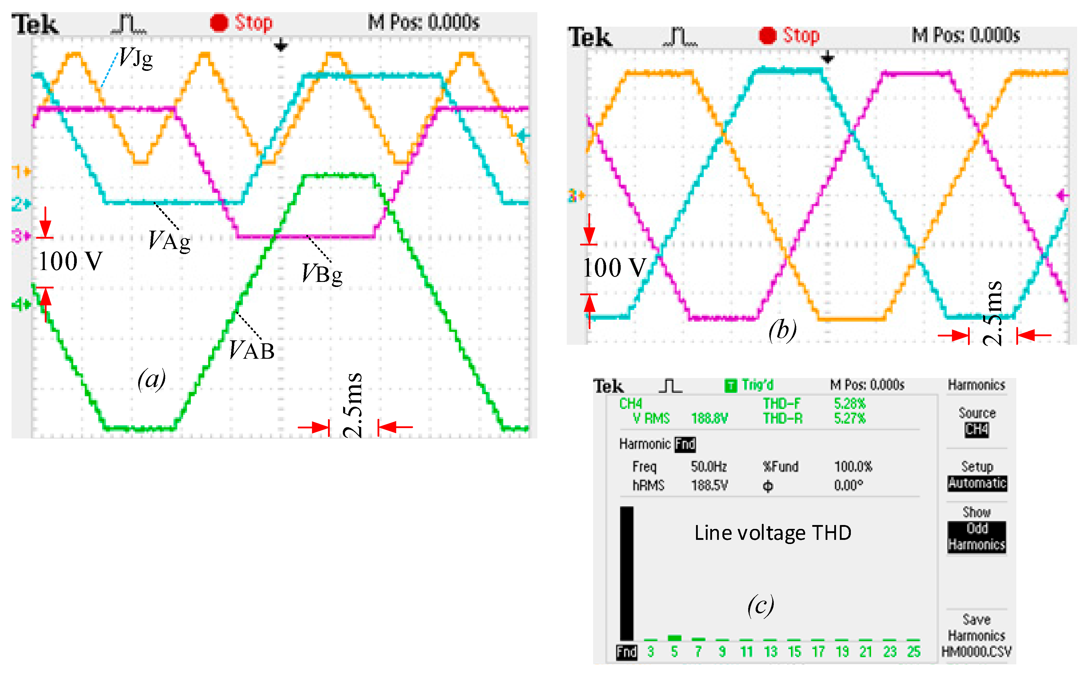
B. H-bridge cells Trinary-related input supplies
In the proposed topology, the number of levels in the output voltages can be increased by considering asymmetric trinary ratio for the input dc supplies. According to (3) the magnitudes of V1, V2, V3 are set to 20 V, 60 V, 180 V; respectively and hence the magnitude of VC is 280 V.
This configuration is able to generate 15-levels (NP = 15) in the pole voltage and 29-levels in the line voltage. Hence, it needs 84-switching states to generate three-phase output voltages according to (5). Table A4 in the Appendix A shows the switching logics for generating 15 levels in the pole voltage. The junction voltage, and line voltage, VAB are shown in Figure 10a. Figure 10b shows 29-level three-phase line voltages on the same plot. The THD of the unfiltered 29-level line voltages is nearly 5% as shown in Figure 10c.
C. Three-phase conversion of existing single-phase inverter topologies
A number of single phase MLI topologies along with different input voltage algorithms have been recently published [12,13,14,15,17,18,19,20,21,22,23]. The proposed three-phase inverter concept in this paper permits easy conversion of the existing single phase MLI into three-phase structures without tripling the number of semiconductor switches and dc-supplies as per the current conventional practice. To do so, only the PG stage in the proposed topology is required to be connected with any existing single phase topology.
To extend any existing single-phase inverter to three-phase structure using the proposed concept, switching logics of the single phase cascaded inverter can be retained. Figure 11a shows a single phase topology published in [12] while Figure 11b shows the extended three-phase structure of this single phase inverter using the proposed concept in this paper. As shown in Figure 11b, the single phase topology acts as a cascaded stage and generates all possible voltage levels by following the same switching logic proposed in [12].
The bidirectional and CTPTLI switches operate as shown in Figure 2. In [12], the single phase structure produces 15-levels in the line voltage, when Figure 12a is set with V11 = V21 = V31 = V21 = V22 = V23 = V’0 = 40 V and VC = 280 V. The cascaded stage in Figure 11b is arranged in a similar pattern by imitating the single-phase structure for three-phase conversion.
Figure 11b, the single phase topology acts as a cascaded stage and generates all possible voltage levels by following the same switching logic proposed in [12]. The bidirectional and CTPTLI switches operate as shown in Figure 2. In [12], the single phase structure produces 15-levels in the line voltage, when Figure 12a is set with V11 = V21 = V31 = V21 = V22 = V23 = V’0 = 40 V and VC = 280 V. The cascaded stage in Figure 11b is arranged in a similar pattern by imitating the single-phase structure for three-phase conversion.
Table 1 provides a comparison of using the concept proposed in this paper and conventional methods to transfer single-phase to three-phase structure.
The table reveals the superior advantages of the proposed concept over existing conventional methods in terms of reducing the number of switches and dc-supplies while increasing the levels in the output voltages when a single phase structure is extended to three-phase one.
The three-phase inverter in Figure 11b produces nine levels in the pole voltages and 17-levels in the line voltage. It requires 48-switching states to produce these voltage levels according to (5). Table A5 in the Appendix A shows the switching logic for this inverter. Figure 12a shows the junction voltage, VJg, pole voltages and line voltage, VAB of the extended three-phase inverter. Figure 12b shows the three-phase 17-level line voltages on the same plot.

6. Semiconductor Losses and Inverter Efficiency

Semiconductor losses are considered as a crucial design factor for any converter circuit, which influences and defines the required thermal management and contributes to the estimation of overall cost, volume and weight of the inverter. There are two dominant losses in the semiconductor devices; the static and the dynamic losses. The on-state resistance and the forward voltage drop of the semiconductor device are responsible for the static (conduction) losses, while the dynamic losses are produced during the ON-OFF actions dictated by the switching frequency of the device [39].
The overall semiconductor losses of the proposed CMLI can be estimated by the total conduction and switching losses of all used semiconductors as below:
P t o t a l _ l o s s = P c ( t ) + P s w
If the output power is Pout, the inverter efficiency (ƞ) can be calculated from:
η % = ( P o u t P t o t a l _ l o s s + P o u t ) × 100 %
The output power is calculated from:
P o u t = 3 × V C 2 × I l i n e 2 × P F
where VC and Iline are the input voltage to the CTPTLI and output line current, respectively.
The proposed topology (Figure 4b) in this paper utilizes IGBT with anti-parallel diode (HGTG20N60B3D) in the cascaded structure and IGBT (IRG4BC40W) along with diode (RHRP1540) in the PG structure. The following parameters are used to calculate the switching losses; VT = 1.8 V, RT = 0.10, VD = 1.2 V, RD = 0.1, β = 1, ton = toff = 1 µs. where, the on-state voltage drop of the transistor and diode are expressed by VT and VD, respectively. The on-state resistances of the transistor and diode, are given by RT and RD, respectively. The transistor amplification factor and ON-OFF time is expressed by ‘β’, ton and toff, respectively.
Total switching loss is found to be Ptotal_loss = 2.9067 watt with 1.3076 watt losses associated in the cascaded stage and 1.5991 watt in the PG stage. For a connected load of 0.82 lagging power factor (PF) and by using (15), the output power is 98.64 watt which gives an overall efficiency of about 97%.

7. Comparison with Other Topologies

As shown in the results section, the proposed three-phase MLI concept can be adopted to extend any existing single-phase topology to three-phase without tripling the used components as per the current conventional methods. Furthermore, the proposed concept is able to reduce the size of the existing three-phase cascaded MLI topologies in terms of device count without degrading the quality of the output voltage. A comparison is performed in order to show the effectiveness of the proposed three-phase cascaded MLI concept over various existing topologies. Different factors such as number of power semiconductor components, number of gate driver circuits and number of dc-supplies are considered in the comparison.
Table 2 shows a comparison among existing three-phase CHB MLI topologies and the three-phase MLI concept proposed in this paper. The CHB inverter proposed in [35], has two CHB cells and binary relation is maintained between the input dc-supplies in each phase arm.
On the other hand, trinary related three and four CHB cells in each phase arm is considered in [38,42], respectively. A significant reduction in the device count can be realized when the new three-phase cascaded MLI concept is applied to these existing topologies as can be seen in Table 2. The percentage of reduction of device count and the input dc supplies is increasing when the number of CHB cells in each phase arm is increasing. For example, 17% reduced power electronic components is achieved in the proposed three-phase cascaded MLI concept for two CHB cell, while 33% and 42% reduction will be achieved when the proposed concept is applied for three and four CHB cells in each phase arm of the existing topologies, respectively.

8. Conclusions

This paper presents a new design for a three-phase CHB MLI. Experimental results validate the practical feasibility of the proposed three-phase MLI concept. Comparison with published three-phase MLI topologies shows the superiority of the proposed concept over existing topologies in terms of reduced device count without compromising the quality of the output voltage. Moreover, the proposed concept can be adopted to extend any single phase MLI to three-phase structures without tripling its components as per the current practice. The new technique can be adopted by existing three-phase topologies to reduce its device count without degrading the overall performance. Since the number of components is directly related to the cost, complexity and the installation area, the new three-phase concept is a cost-effective technique that is expected to have a great potential for renewable power generation systems and smart grid applications.

Acknowledgments

The authors would like to acknowledge the contribution of an Australian Government Research Training Program Scholarship in supporting this research.

Author Contributions

Md Mubashwar Hasan conceived, designed the laboratory prototype and conducted the experiments; A. Abu-Siada and Syed M. Islam contributed in analyzing data and results; S. M. Muyeen took part while writing the paper.

Conflicts of Interest

The authors declare no conflict of interest.

Appendix A

Table A1. Generalized switching logic for a cascaded cell.
VoutTurn on Switches
VkGk1, Gk3
0Gk1, Gk4
VkGk2, Gk4
Table A2. Switching logic for different switching vector.
Switching Vector, Sa/Sb/ScSwitching Logic
4Figure 5a
3Figure 5b
2Figure 5c
1Figure 5d
0Figure 5e
Table A3. System specifications of the implemented inverter.
Input DC Source Voltage in CHB Stage (V1, V2, V3)70 V Each
Input DC source voltage in PGS (VC)280 V
Switching frequency50 Hz
Magnitude of line voltages280 V (Peak)
Load power factor0.82
Tested power of the prototype523 Watt
Number of levels in the peak–peak line voltages9
Table A4. Switching logic for generating 15 levels in the pole voltage.
Switching Vector, SaPole VoltageSwitching Logic
14VC280 VFigure 5a
13v + 3v + 9v260 VV1 + V2 + V3BD-Switch-A ON
120 + 3v + 9v240 V0 + V2 + V3
11v + 3v + 9v220 VV1 + V2 + V3
10v + 0 + 9v200 VV1 + 0 + V3
90 + 0 + 9v180 V0 + 0 + V3
8v + 0 + 9v160 VV1 + 0 + V3
7v − 3v + 9v140 VV1V2 + V3
60 − 3v + 9v120 V0 − V2 + V3
5v − 3v + 9v100 VV1V2 + V3
4v + 3v + 080 VV1 + V2 + 0
30 + 3v + 060 V0 + V2 + 0
2v + 3v + 040 VV1 + V2 + 0
1v + 0 + 020 VV1 + 0 + 0
000Figure 5e
Table A5. Switching logic in the cascaded stage and PG-stage for generating 9 levels in the pole voltage, VAg.
Switching VectorPole Voltage (V)Switching Logic
00Figure 5a
120S1, S51, S52BD-Switch-A Turn ON
240S2, S11, S31, S41, S52
360S1, S11, S31, S41, S52
480S1, S11, S21, S31, S52
5100S2, S11, S21, S31, S12, S32, S42
6120S2, S11, S21, S31, S12, S22, S32
7140S1, S11, S21, S31, S12, S22, S32
8160Figure 5e

References

  1. Kawamura, W.; Hagiwara, M.; Akagi, H.; Tsukakoshi, M.; Nakamura, R.; Kodama, S. AC-Inductors Design for a Modular Multilevel TSBC Converter, and Performance of a Low-Speed High-Torque Motor Drive Using the Converter. IEEE Trans. Ind. Appl. 2017, 53, 4718–4729. [Google Scholar] [CrossRef]
  2. Hasan, M.M.; Mekhilef, S.; Ahmed, M.; Messikh, T. Three-phase multilevel inverter with high value of resolution per switch employing a space vector modulation control scheme. Turk. J. Electr. Eng. Comput. Sci. 2016, 24, 1993–2009. [Google Scholar] [CrossRef]
  3. Hasan, M.M.; Ahmed, M.; Mekhilef, S. Analyses and simulation of three-phase MLI with high value of resolution per switch employing SVM control scheme. In Proceedings of the 2012 IEEE International Conference on Power and Energy (PECon), Kota Kinabalu, Malaysia, 2–5 December 2012; pp. 7–12. [Google Scholar]
  4. Hasan, M.M.; Abu-Siada, A. A high frequency linked modular cascaded multilevel inverter. In Proceedings of the 2016 IEEE Industrial Electronics and Applications Conference (IEACon), Kota Kinabalu, Malaysia, 20–22 November 2016; pp. 47–51. [Google Scholar]
  5. Hasan, M.M.; Abu-Siada, A. A novel three-phase cascaded multilevel inverter topology. In Proceedings of the 2016 IEEE Industrial Electronics and Applications Conference (IEACon), Kota Kinabalu, Malaysia, 20–22 November 2016; pp. 31–35. [Google Scholar]
  6. Kouro, S.; Malinowski, M.; Gopakumar, K.; Pou, J.; Franquelo, L.G.; Wu, B.; Rodriguez, J.; Perez, M.A.; Leon, J.I. Recent advances and industrial applications of multilevel converters. IEEE Trans. Ind. Electron. 2010, 57, 2553–2580. [Google Scholar] [CrossRef]
  7. Franquelo, L.G.; Rodriguez, J.; Leon, J.I.; Kouro, S.; Portillo, R.; Prats, M.A. The age of multilevel converters arrives. IEEE Ind. Electron. Mag. 2008, 2. [Google Scholar] [CrossRef]
  8. Kawakami, N.; Ota, S.; Kon, H.; Konno, S.; Akagi, H.; Kobayashi, H.; Okada, N. Development of a 500-kW modular multilevel cascade converter for battery energy storage systems. IEEE Trans. Ind. Appl. 2014, 50, 3902–3910. [Google Scholar] [CrossRef]
  9. Hasan, M.M.; Abu-Siada, A.; Islam, M.R. Investigation of low switching frequency control of a three-phase cascaded H-bridge multilevel inverter. In Proceedings of the 2016 International Conference on Electrical, Computer & Telecommunication Engineering (ICECTE), Rajshahi, Bangladesh, 8–10 December 2016; pp. 1–5. [Google Scholar]
  10. Inoue, S.; Akagi, H. A bidirectional isolated DC–DC converter as a core circuit of the next-generation medium-voltage power conversion system. IEEE Trans. Power Electron. 2007, 22, 535–542. [Google Scholar] [CrossRef]
  11. Dixon, J.; Pereda, J.; Castillo, C.; Bosch, S. Asymmetrical multilevel inverter for traction drives using only one DC supply. IEEE Trans. Veh. Technol. 2010, 59, 3736–3743. [Google Scholar] [CrossRef]
  12. Babaei, E.; Laali, S.; Bayat, Z. A single-phase cascaded multilevel inverter based on a new basic unit with reduced number of power switches. IEEE Trans. Ind. Electron. 2015, 62, 922–929. [Google Scholar] [CrossRef]
  13. Hasan, M.M.; Abu-Siada, A.; Dahidah, M.S.A. A Three-Phase Symmetrical DC-Link Multilevel Inverter with Reduced Number of DC Sources. IEEE Trans. Power Electron. 2017. [Google Scholar] [CrossRef]
  14. Kangarlu, M.F.; Babaei, E.; Laali, S. Symmetric multilevel inverter with reduced components based on non-insulated dc voltage sources. IET Power Electron. 2012, 5, 571–581. [Google Scholar] [CrossRef]
  15. Khosroshahi, M.T. Crisscross cascade multilevel inverter with reduction in number of components. IET Power Electron. 2014, 7, 2914–2924. [Google Scholar] [CrossRef]
  16. Hasan, M.M.; Abu-Siada, A.; Islam, S.M.; Muyeen, S.M. A three-phase half-bridge cascaded inverter with reduced number of input DC supply. In Proceedings of the 2017 Australasian Universities Power Engineering Conference (AUPEC), Melbourne, Australia, 19–22 November 2017. [Google Scholar]
  17. Alishah, R.S.; Hosseini, S.H.; Babaei, E.; Sabahi, M. Optimization Assessment of a New Extended Multilevel Converter Topology. IEEE Trans. Ind. Electron. 2017, 64, 4530–4538. [Google Scholar] [CrossRef]
  18. Alishah, R.S.; Hosseini, S.H.; Babaei, E.; Sabahi, M. Optimal Design of New Cascaded Switch-Ladder Multilevel Inverter Structure. IEEE Trans. Ind. Electron. 2017, 64, 2072–2080. [Google Scholar] [CrossRef]
  19. Thamizharasan, S.; Baskaran, J.; Ramkumar, S.; Jeevananthan, S. Cross-switched multilevel inverter using auxiliary reverse-connected voltage sources. IET Power Electron. 2014, 7, 1519–1526. [Google Scholar] [CrossRef]
  20. Kangarlu, M.F.; Babaei, E. Cross-switched multilevel inverter: An innovative topology. IET Power Electron. 2013, 6, 642–651. [Google Scholar] [CrossRef]
  21. Kangarlu, M.F.; Babaei, E.; Sabahi, M. Cascaded cross-switched multilevel inverter in symmetric and asymmetric conditions. IET Power Electron. 2013, 6, 1041–1050. [Google Scholar] [CrossRef]
  22. Gupta, K.K.; Jain, S. Multilevel inverter topology based on series connected switched sources. IET Power Electron. 2013, 6, 164–174. [Google Scholar] [CrossRef]
  23. Gupta, K.K.; Jain, S. A novel multilevel inverter based on switched DC sources. IEEE Trans. Ind. Electron. 2014, 61, 3269–3278. [Google Scholar] [CrossRef]
  24. Karasani, R.R.; Borghate, V.B.; Meshram, P.M.; Suryawanshi, H.M.; Sabyasachi, S. A Three-Phase Hybrid Cascaded Modular Multilevel Inverter for Renewable Energy Environment. IEEE Trans. Power. Electron. 2017, 32, 1070–1087. [Google Scholar] [CrossRef]
  25. Hasan, M.; Mekhilef, S.; Ahmed, M. Three-phase hybrid multilevel inverter with less power electronic components using space vector modulation. IET Power Electron. 2014, 7, 1256–1265. [Google Scholar] [CrossRef]
  26. Su, G.-J. Multilevel dc-link inverter. IEEE Trans. Ind. Appl. 2005, 41, 848–854. [Google Scholar] [CrossRef]
  27. Ruiz-Caballero, D.A.; Ramos-Astudillo, R.M.; Mussa, S.A.; Heldwein, M.L. Symmetrical hybrid multilevel DC–AC converters with reduced number of insulated DC supplies. IEEE Trans. Ind. Electron. 2010, 57, 2307–2314. [Google Scholar] [CrossRef]
  28. Waltrich, G.; Barbi, I. Three-phase cascaded multilevel inverter using power cells with two inverter legs in series. IEEE Trans. Ind. Electron. 2010, 57, 2605–2612. [Google Scholar] [CrossRef]
  29. Elias, M.F.M.; Rahim, N.A.; Ping, H.W.; Uddin, M.N. Asymmetrical cascaded multilevel inverter based on transistor-clamped H-bridge power cell. IEEE Trans. Ind. Appl. 2014, 50, 4281–4288. [Google Scholar] [CrossRef]
  30. Colak, I.; Kabalci, E.; Bayindir, R. Review of multilevel voltage source inverter topologies and control schemes. Energy Convers. Manag. 2011, 52, 1114–1128. [Google Scholar] [CrossRef]
  31. Mortezaei, A.; Simões, M.G.; Bubshait, A.S.; Busarello, T.D.C.; Marafão, F.P.; Al-Durra, A. Multifunctional control strategy for asymmetrical cascaded H-bridge inverter in microgrid applications. IEEE Trans. Ind. Appl. 2017, 53, 1538–1551. [Google Scholar] [CrossRef]
  32. Prabaharan, N.; Palanisamy, K. A comprehensive review on reduced switch multilevel inverter topologies, modulation techniques and applications. Renew. Sustain. Energy Rev. 2017, 76, 1248–1282. [Google Scholar] [CrossRef]
  33. Tolbert, L.M.; Zheng, P.F.; Habetler, T.G. Multilevel PWM methods at low modulation indices. IEEE Trans. Power. Electron. 2000, 15, 719–725. [Google Scholar] [CrossRef]
  34. Islam, S.M.; Nayar, C.V.; Abu-Siada, A.; Hasan, M.M. Power Electronics for Renewable Energy Sources. In Power Electronics Handbook, 4th ed.; Elsevier: Amsterdam, The Netherlands, 2018; pp. 783–827. [Google Scholar]
  35. Khoucha, F.; Lagoun, S.M.; Marouani, K.; Kheloui, A.; El Hachemi Benbouzid, M. Hybrid cascaded H-bridge multilevel-inverter induction-motor-drive direct torque control for automotive applications. IEEE Trans. Ind. Electron. 2010, 57, 892–899. [Google Scholar] [CrossRef] [Green Version]
  36. Beig, A.R.; Dekka, A. Experimental verification of multilevel inverter-based standalone power supply for low-voltage and low-power applications. IET Power Electron. 2012, 5, 635–643. [Google Scholar] [CrossRef]
  37. Lee, C.K.; Hui, S.Y.R.; Shu-Hung, C.H. A 31-level cascade inverter for power applications. IEEE Trans. Ind. Electron. 2002, 49, 613–617. [Google Scholar] [CrossRef]
  38. Liu, Y.; Luo, F.L. Trinary hybrid 81-level multilevel inverter for motor drive with zero common-mode voltage. IEEE Trans. Ind. Electron. 2008, 55, 1014–1021. [Google Scholar] [CrossRef]
  39. Hasan, M.M.; Abu-Siada, A.; Islam, M.R. Design and implementation of a novel three-phase cascaded half-bridge inverter. IET Power Electron. 2016, 9, 1741–1752. [Google Scholar] [CrossRef]
  40. Hasan, M.M.; Abu-Siada, A.; Islam, S.M.; Muyeen, S.M. A Novel Generalized Concept for Three-phase Cascaded Multilevel Inverter Topologies. In Proceedings of the 2017 Ninth Annual IEEE Green Technologies Conference (GreenTech), Denver, CO, USA, 29–31 March 2017; pp. 110–117. [Google Scholar]
  41. IEEE Standard for Interconnecting Distributed Resources with Electric Power Systems; IEEE Std. 1547-2003; Institute of Electrical and Electronics Engineers: Piscataway, NJ, USA, 2003; pp. 1–28. [CrossRef]
  42. Pereda, J.; Dixon, J. High-frequency link: A solution for using only one dc source in asymmetric cascaded multilevel inverters. IEEE Trans. Ind. Electron. 2011, 58, 3884–3892. [Google Scholar] [CrossRef]
Figure 1. Block diagrams: (a) level and polarity generators-based cascaded multilevel inverter (CMLI) topology; (b) CMLI topology with no polarity generator; (c) 3-phase CMLI topology; (d) proposed 3-phase CMLI; (e) Circuital model of the PG-stage. Reprint with permission [4261051118814]; 2018, IEEE.
Energies 11 00268 g001
Figure 2. Simplified structure of the proposed CMLI, (a) generation of maximum and zero voltage levels; (b) intermediate level generation; (c) pole voltage waveform. Reprint with permission [4261051118814]; 2018, IEEE.
Energies 11 00268 g002
Figure 3. Conventional three-phase CHB-MLI. Reprint with permission [4261051118814]; 2018, IEEE.
Energies 11 00268 g003
Figure 4. Proposed three-phase CMLI (a) CHB cells are considered as cascaded stage; (b) a standard CHB cell. Reprint with permission [4261051118814]; 2018, IEEE.
Energies 11 00268 g004
Figure 5. Different switching logics for generating four levels in the pole voltages: (a) level 3v; (b) Level 2v; (c) Level v; (d) Level 0; (e) Complete cycle of the pole voltage. Reprint with permission [4261051118814]; 2018, IEEE.
Energies 11 00268 g005
Figure 6. Generalized switching states for generating different number of levels in the pole voltage. Reprint with permission [4261051118814]; 2018, IEEE.
Energies 11 00268 g006
Figure 7. Experimental prototype hardware model. Reprint with permission [4261051118814]; 2018, IEEE.
Energies 11 00268 g007
Figure 8. Experimental results of (a) Junction voltage, and Pole voltages when the CHB-cells are fed by symmetric dc-power supplies; (b) load voltage; (c) load voltage harmonics.
Energies 11 00268 g008
Figure 9. Experimental results, (a) line voltages; (b) line currents; (c) THD of the line voltage; (d) THD of the line current, when CHB cells are fed by Symmetric dc power supplies.
Energies 11 00268 g009
Figure 10. Experimental results, (a) Junction voltage, pole voltages (VAg, VBg), line voltage (VAB); (b) 29-level 3-phase line voltages; (c) THD of the line voltage, when CHB cells are fed by trinary related dc power supplies. Reprint with permission [4261051118814]; 2018, IEEE.
Energies 11 00268 g010
Figure 11. Three-phase conversion of a single phase topology (a) existing single phase topology proposed in [12]; (b) three-phase conversion of existing topology according to the concept proposed in this paper.
Energies 11 00268 g011
Figure 12. Experimental results, (a) Junction voltage, pole voltages (VAg, VBg), line voltages (VAB); (b) 17-level three-phase line voltages.
Energies 11 00268 g012
Table 1. Comparison between three-phase conversion of a single-phase structure using conventional methods and proposed concept in this paper.
TopologySingle Phase StructureConventional 3 Phase ConversionThis Paper Proposed Concept
Line Voltage LevelsSwitchesDC-SuppliesLine Voltage LevelsSwitchesDC-SuppliesLine Voltage LevelsSwitchesDC-Supplies
Non-isolated inverter topology [9]1512715362117248
DC-link half-bridge cascaded inverter [21]1312613361815247
Table 2. Comparison among conventional three-phase CHB topologies and the proposed three-phase cascaded MLI for different asymmetric input voltage arrangements.
CategoryBinary Related Two CHB Cell Topology [35]Trinary Related Three CHB Cell Topology [42]Trinary Related Four CHB Cell Topology [38]
Existing 3-PhaseProposed New ConceptExisting 3-PhaseProposed New ConceptExisting 3-PhaseProposed New Concept
No of levels in line voltage7927298183
No of switches242036244828
No of diodes242036244828
No of gate driver242036244828
No of dc supplies6394125

