Article

Studies on a Hybrid Full-Bridge/Half-Bridge Bidirectional CLTC Multi-Resonant DC-DC Converter with a Digital Synchronous Rectification Strategy

1
Key Laboratory of Smart Grid of Ministry of Education, Tianjin University, Tianjin 300072, China
2
Tianjin Research Institute of Electric Science Co., Ltd. (TRIED), Tianjin 300300, China
*
Author to whom correspondence should be addressed.
Energies 2018, 11(1), 227; https://doi.org/10.3390/en11010227
Submission received: 18 December 2017 / Revised: 12 January 2018 / Accepted: 15 January 2018 / Published: 18 January 2018

Abstract

:
This study presents a new bidirectional multi-resonant DC-DC converter, which is named CLTC. The converter adds an auxiliary transformer and an extra resonant capacitor based on a LLC resonant DC-DC converter, achieving zero-voltage switching (ZVS) for the input inverting switches and zero-current switching (ZCS) for the output rectifiers in all load range. The converter also has a wide gain range in two directions. When the load is light, a half-bridge configuration is adopted instead of a full-bridge configuration to solve the problem of voltage regulation. By this method, the voltage gain becomes monotonous and controllable. Besides, the digital synchronous rectification strategy is proposed in forward mode without adding any auxiliary circuit. The conduction time of synchronous rectifiers equals the estimation value of body diodes’ conduction time with the lightest load. Power loss analysis is also conducted in different situations. Finally, the theoretical analysis is validated by a 5 kW prototype.

1. Introduction

With advantage of ZVS + ZCS, the bidirectional resonant DC-DC converter (BRDC) is gaining more attention in DC distribution system or DC microgrid applications [1,2,3,4,5,6,7,8]. All the power switching devices, including metal oxide semiconductor field effect transistor (MOSFET) switches and diodes have the desirable soft-switching features, and the switching loss is greatly decreased. In addition, the electromagnetic interference (EMI) is also restricted. As a result, BRDCs are characterized by high efficiency, high power density and low EMI, and are applicable to high frequency applications [9,10]. Among all the BRDCs, the bidirectional series resonant converter (BSRC) is a candidate topology [11,12,13,14,15,16]. All the switches of a BSRC work in either ZVS or ZCS for a wide variation of voltage gains with phase-shift control [13]. A novel control scheme was developed for BSRC in discontinuous mode [14]. With the accumulation of energy packets to raise output voltage, it is possible to have a gain greater than one. A novel method for analyzing the frequency response is also presented based on a mixture of the Fourier and the average state-space methods [15]. The analysis method provides enough information to properly control the BSRC. A BSRC using a continuous current mode was proposed in [16]. Experimental results from a 6 kW prototype validated the theoretical analysis, and higher efficiency is obtained compared to the phase-shift DAB in a wide power range. However, the efficiency is not ideal for the whole frequency range. A bidirectional LLC resonant DC-DC converter is also a good option. A bidirectional three-level LLC resonant converter has a very wide voltage gain range with PWAM control [17]. It overcomes the limitation of voltage gain in LLC resonant converters. A bidirectional LLC resonant converter with automatic forward and backward mode transition is proposed in [18]. An auxiliary inductor is added to raise the voltage gain in backward operation. Based on LLC, a symmetrical bidirectional CLLC resonant converter was recently proposed [19,20,21]. The voltage gain in backward operation is the same as that in forward operation. However, with the growth of output power and voltage conversion ratio, the resonant inductance is small and the resonant capacitance is big. These parameters are hard to design.
Besides, the regulation capability of a resonant DC-DC converter is weak under light load conditions. Due to parasitic parameters in the resonant tank, the output voltage goes up as the switching frequency increases, and an upturn drifting occurs in the voltage gain curve [22]. This phenomenon causes trouble for voltage regulation under light load conditions. To solve this problem, many researchers have changed the control method for light load conditions [23,24,25,26,27,28]. Burst mode is used in [23,24], but the ripple of the output voltage is large and the dynamic response is slow. The phase-shift and PWM control methods are effective in [25,26,27,28], but the control scheme is complex due to the additional control elements. The changes are also conducted with the topology of resonant DC-DC converter. Adding an additional output capacitor to switches can reduce current ripple and decrease powering transmitted between two sides of transformer [29], but the ZVS range this time is narrow. An additional capacitor is paralleled with the resonant inductor to improve the gain characteristics in [30]. ZVS is acquired under entire load condition, and efficiency is improved with less turn-off loss, but the design of the transformer and additional capacitor is complex due to resonance between leakage inductor and the additional capacitor.
The synchronous rectification (SR) strategy for resonant converters is also important toward achieving working efficiency [31,32,33,34]. A novel driving scheme with a compensation network for synchronous rectifiers is used in LLC resonant converters. The conduction loss and switching loss are also reduced considerably [35]. A hybrid driving scheme for full-bridge SR is proposed in [36]. It uses one transformer auxiliary winding to drive two high-side SR switches and a simple current transformer (CT) to drive two low-side SR switches. The proposed method operates well under DCM and CCM conditions. A novel SR control strategy is developed, through accurately tracking the target switching moments in [37]. However, the strategies above are complex in application and they are not verified in BRDCs. A new synchronous rectification strategy, which is simpler and compatible to bidirectional power flow, needs to be developed.
In this study, a new bidirectional CLTC multi-resonant DC-DC converter is proposed. As Figure 1 shows, the converter is composed of a high-voltage side (HVS) full-bridge, low-voltage side (LVS) full-bridge and a multi-resonant tank. An auxiliary transformer T2 and an extra resonant capacitor Cr2 are added on bidirectional LLC resonant DC-DC converter, so the converter is named by CLTC. The gain range in two directions is broadened with the added devices. ZVS for the input inverting switches and ZCS for the output rectifiers are realized in all load range. UH represents HVS DC voltage, while UL represents LVS DC voltage. Power flows in both forward and backward mode are modulated with pulse frequency modulation (PFM). In forward mode, S1 & S4 and S2 & S3 run with 50% duty cycle, the rectifier switches S6 & S7 and S5 & S8 are driven by the SR signals. In backward mode, S6 & S7 and S5 & S8 run at 50% duty cycle, S1 & S4 and S2 & S3 don’t work, diodes on HVS realize SR.
This paper is organized as follows: the operation principles and characteristic descriptions of the proposed converter are discussed in Section 2. Hybrid full-bridge/half-bridge configuration is used to improve the light load regulation capability in Section 3. Stresses of power devices, load and working frequency range in half-bridge CLTC are also given to prove the feasibility of the half-bridge configuration. SR strategy based on estimation of the diodes’ conduction time is proposed in Section 4. Power loss distribution and comparison tests are conducted with different loads and LVS DC voltages in Section 5. A 5 kW prototype is built with HVS voltage of 400 V and LVS DC voltage of 42–58 V. Experimental results are shown to validate the theoretical analysis above in Section 6. Conclusions are drawn in Section 7.

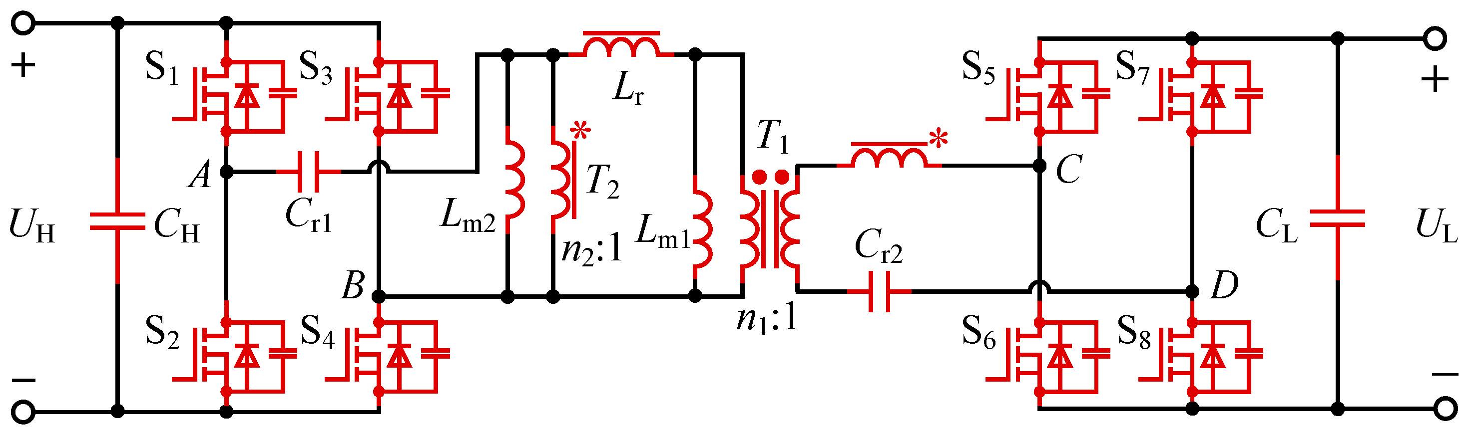
2. Operation Principles and Characteristic Description

In this section, the main operation principles of CLTC multi-resonant converter are given. It is similar to a LLC resonant converter as two stages of resonance exist. The resonant frequency, voltage gain and ZVS characteristic are analyzed, forming research foundations for the following sections.

2.1. Operation Principles

Figure 2 shows different states of the CLTC multi-resonant converter. In Figure 2, iLm1 is excitation current of transformer T1 on HVS, i’Lm1 is excitation current of transformer T1 on LVS, iLr is current of resonant inductor, iCr1 and iCr2 are currents of resonant capacitors on HVS and LVS, uGS14 is the driving signal of S1 and S4, uGS23 is the driving signal of S2 and S3, uGS58 is the driving signal of S5 and S8, uGS67 is the driving signal of S6 and S7, uDS14 is the drain-source voltage of S1 and S4, uDS23 is the drain-source voltage of S2 and S3, uDS58 is the drain-source voltage of S5 and S8, uDS67 is the drain-source voltage of S6 and S7, iDS14 is the drain-source current of S1 and S4, iDS23 is the drain-source current of S2 and S3, iDS58 is the drain-source current of S5 and S8, iDS67 is the drain-source current of S6 and S7.

2.1.1. Forward Mode

The equivalent circuits in forward mode are listed in Figure 3. Detailed descriptions and explanations of the operational modes in half period are as follows:
Mode A [t0t1]: S2 and S3 have just turned off at t0. The HVS current charges the output capacitor of S2 and S3, and discharges the output capacitor of S1 and S4. After that, the HVS current passes through the antiparallel diode of S1 and S4, which makes the switches turn on under the ZVS condition.
Mode B [t1t2]: At t1, S1, S4, S5 and S8 turn on and power is transferred from HVS to LVS. The resonant current changes in a sine-wave with main resonant frequency, fr. At t2, iLr is equal to iLm1, iCr2 and ids58 become zero.
Mode C [t2t3]: S1 and S4 are still on in this mode, S5 and S8 are off in this mode. As iCr2 and ids58 are zero in t2, S5 and S8 turn off under ZCS condition. The HVS goes into secondary resonance with the frequency of fr2f. At t3, S1 and S4 are off and ready to go into dead-time duration.
When working frequency is bigger than main resonant frequency, Mode C and ZCS of LVS power switches disappear like LLC. The turn-off currents increase largely in this situation.

2.1.2. Backward Mode

The equivalent circuits in backward mode are listed in Figure 4. Lm1 and Lm2 are the magnetizing inductors on LVS. The modes are similar to those in forward mode. Detail descriptions and explanations of the operational modes in half period are shown as follows:
Mode A [t0t1]: S6 and S7 turn off at t0. The resonant current on LVS charges the output capacitor of S6 and S7, and discharges the output capacitor of S5 and S8. After that, the LVS current passes through the antiparallel diode of S5 and S8, which makes the switches turn on under the ZVS condition.
Mode B [t1t2]: At t1, S5, S8, D1 and D4 turn on and power is transferred from LVS to HVS. The resonant current on LVS changes in a sine-wave with main resonant frequency. At t2, iCr2 is equal to i’Lm1, iCr1 and ids14 become zero.
Mode C [t2t3]: S5 and S8 are still on in this mode, D1 and D4 are off in this mode. ZCS of D1 and D4 is realized as iCr1 and ids14 become zero at t2. The LVS goes into secondary resonance with the frequency of fr2b. At t3, S1 and S4 are off and ready to go into dead-time duration.
When working frequency is bigger than main resonant frequency, Mode C and ZCS of HVS diodes disappear like LLC. The turn-off currents increase largely in this situation.

2.2. Characteristic Description

Main resonant frequency of CLTC converter in two power flows, fr, is:
f r = 1 2 π A B
where:
A = A 1 + A 1 2 A 2
A 1 = C r 1 L m 2 ( L m 1 + L r ) n 1 2 n 2 2 + ( L m 1 + L r ) C r 2 L m 2 n 1 2 + ( L m 2 + L r ) C r 2 L m 1 n 2 2 + 2 C r 2 L m 1 L m 2 n 1 n 2
A 2 = 4 C r 1 C r 2 L m 1 L m 2 L r ( L m 1 + L m 2 + L r ) n 1 2 n 2 4
B = 2 C r 1 C r 2 L m 1 L m 2 L r n 2 2
fr is obtained when no load is added and imaginary part of AC input impedance of CLTC is zero.
The secondary resonant frequency in forward mode, fr2f, and the secondary resonant frequency in backward mode, fr2b, are:
f r 2 f = 1 2 π L r + L m 1 + L m 2 C r 1 L m 2 ( L r + L m 1 )
f r 2 b = 1 2 π ( L m 1 + L m 2 ) C r 2
fr2f and fr2b are obtained with the resonant capacitance and inductance in secondary resonance. The resonant capacitance and inductance are shown in Figure 3c and Figure 4c.
By use of the fundamental harmonic analysis (FHA) method, Figure 5a and Figure 6a show 3D voltage gain curves according to load Po and normalized working frequency fs/fr. GF is gain in forward mode and GB is gain in backward mode. As is shown in Figure 5b and Figure 6b, when the working frequency is below the main resonant frequency, GF and GB increase at first and decrease subsequently with the growth of working frequency. The peak gains are more than 1 over all the load range and obtained around secondary resonant frequency, fr2f and fr2b. At main resonant frequency fr, the gain of the converter is 1. As is shown in Figure 5c and Figure 6c, when working frequency is above main resonant frequency, GF and GB decrease with the growth of working frequency. When load is lighter, the voltage gain is higher and the slope of gain curve is sharper. Voltage gain range of CTLC converter is wide enough to adapt applications like battery charger and DC microgrid.
In order to realize ZVS for HVS switches, in forward mode, the dead-time duration tdt_F should satisfy (6) using the ZVS mechanism analyzed by [19]. Coss_H is the output capacitance of HVS switch:
t dt _ F 16 C oss _ H L m 2 ( L r + L m 1 ) f s L r + L m 1 + L m 2
Similarly, in backward mode, the dead-time duration tdt_B of LVS switches should satisfy:
t dt _ B 16 C oss _ L ( L m 1 + L m 2 ) f s
Coss_L is the output capacitance of LVS switch in (7).
The inequations can be easily satisfied with different loads and working frequencies, which is good for efficiency. The tdt_F and tdt_B are set to 200 ns in experiments.

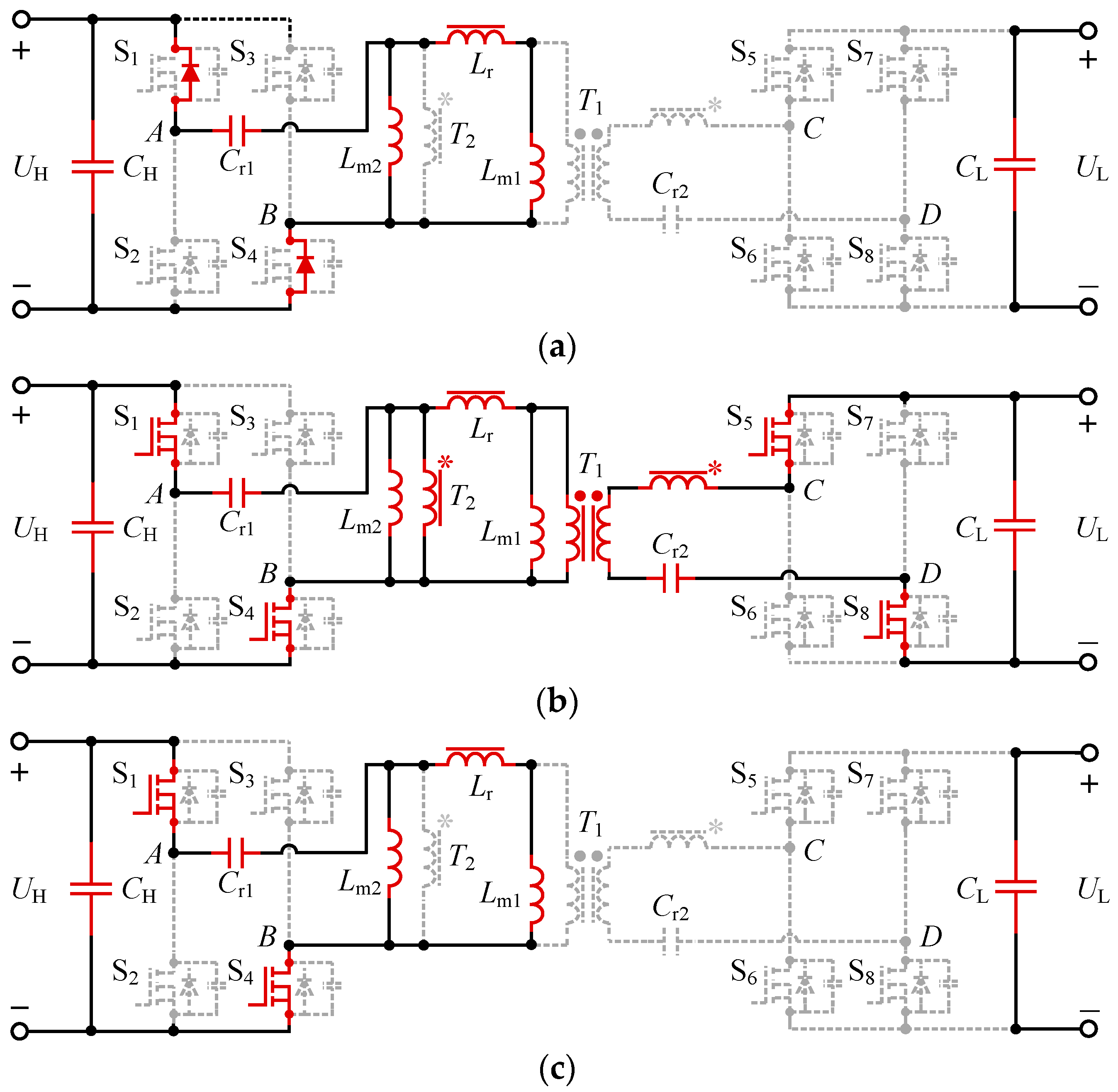
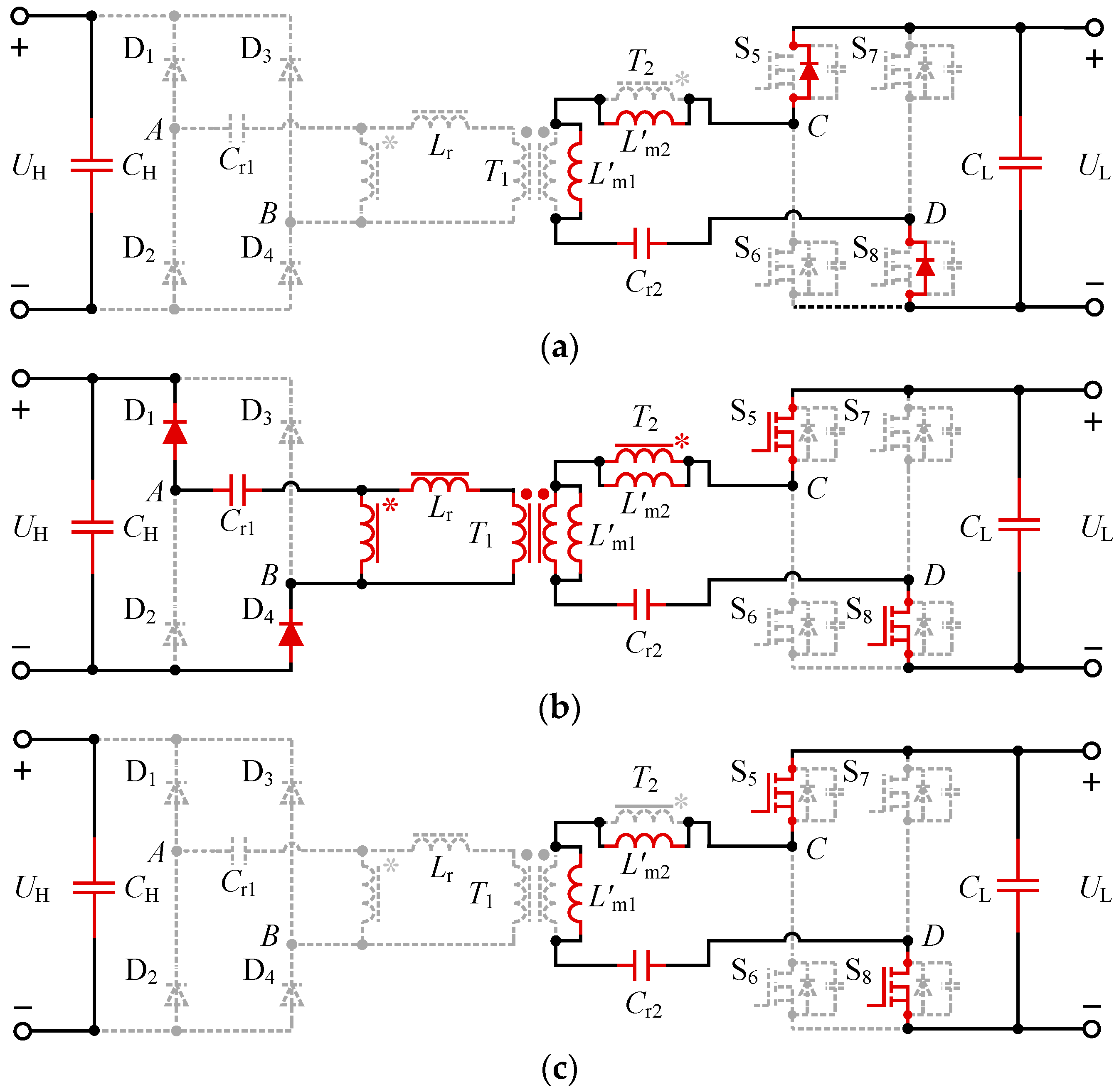
3. Hybrid Full-Bridge/Half-Bridge Configuration

In this section, the reason for the upturn phenomenon is analyzed. A full-bridge configuration is used with a normal load. Half-bridge configurations are used for light load conditions with the advantage of monotonous gain curve and lower frequency. Because the situations in forward and backward mode are similar, the discussion in this section is conducted only in forward mode, and details are not provided for the backward mode.

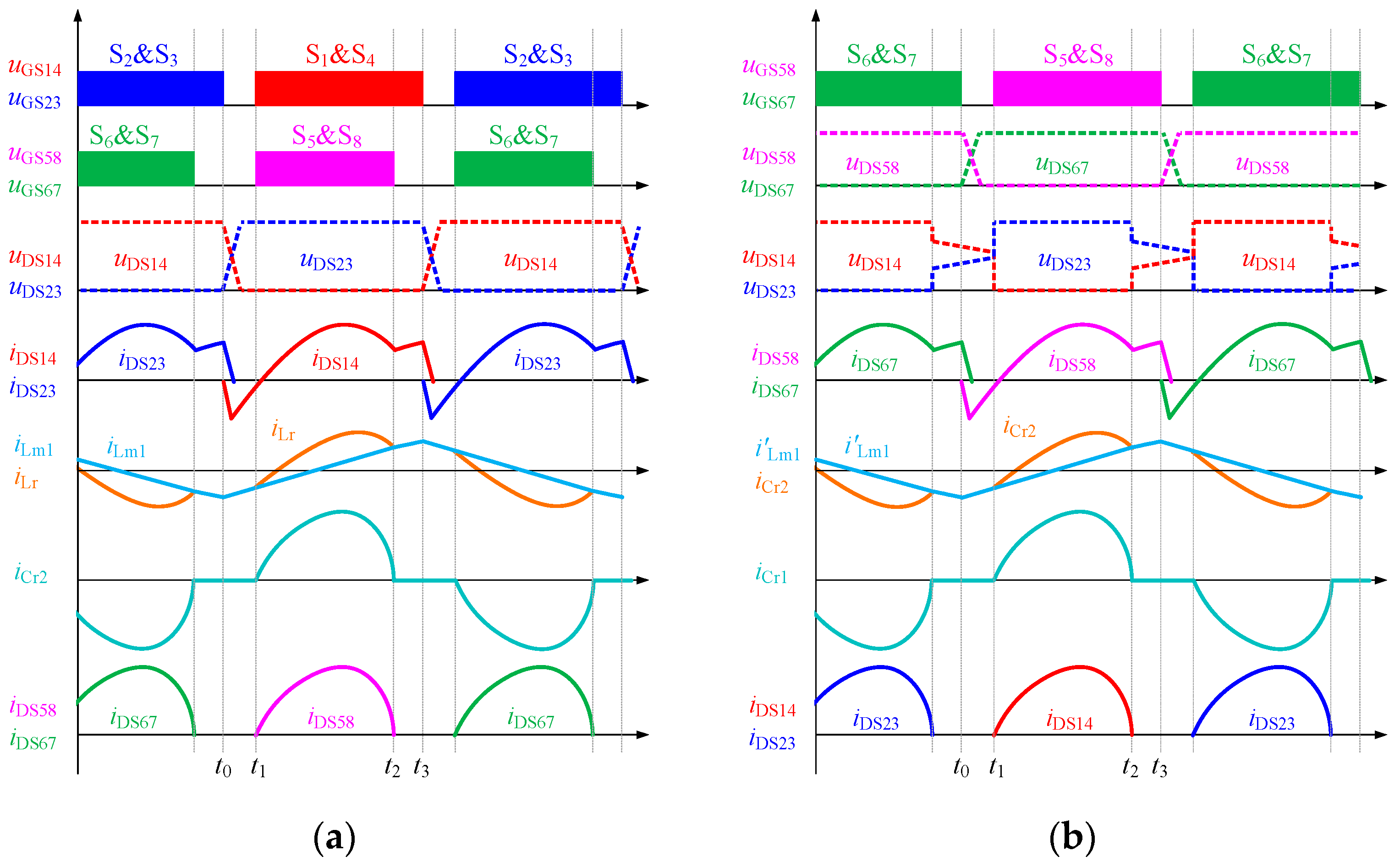
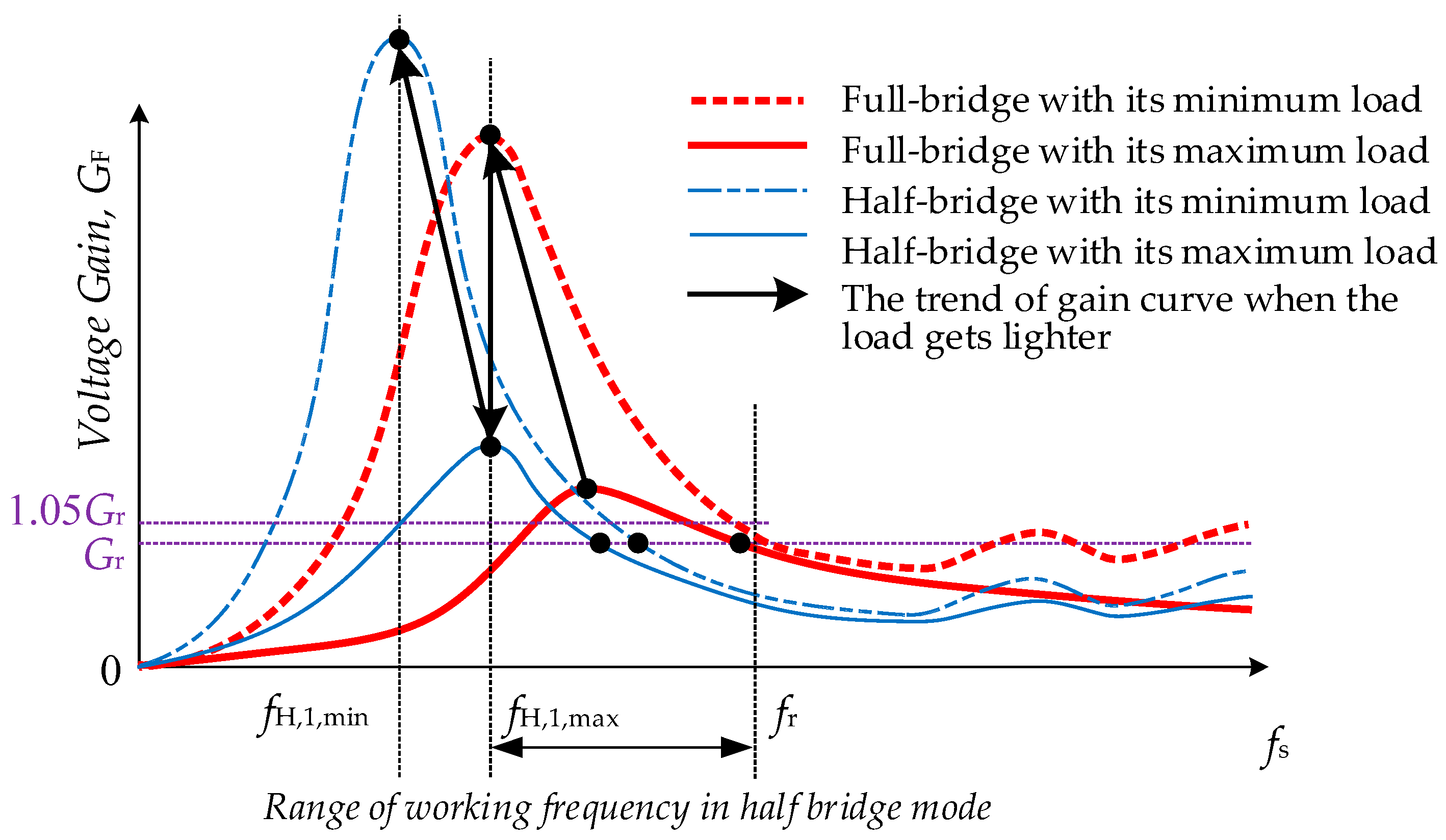
3.1. Half-Bridge Configuration at Light Load Condition

Using the analysis method proposed in [22], it is found that transformer wiring capacitance is the main factor leading to the upturn problem. As is shown in Figure 7a, the ideal gain curve without considering parasitic parameters in forward mode is monotonous with working frequency under light load conditions. However, the voltage gain curve considering transformer wiring capacitance and experimental gain curve has upturns. As the experiment gain curve is not monotonous, the gain cannot be regulated well with PFM. For example, the voltage gain of 1.02 in Figure 7a is obtained with four different working frequencies. When PFM is adopted to control LVS voltage, the working frequency may be around 1.4fr instead of 0.8fr, and fluctuates quickly as the gain curve is not monotonous.
To overcome the above problem, a half-bridge configuration is introduced in this paper to regulate the required output voltage. In forward mode, the full-bridge in HVS is transformed into a half-bridge by turning off Q3 and turning on Q4 incessantly. The voltage gain is reduced by half, with the same load and resonant parameters. Thus, when the voltage gain needed is below 1 under light load conditions, a half-bridge configuration is adopted and the required gain is obtained with lower working frequency. In Figure 7b, when the working frequency is around 0.35fr, twice the required gain is acquired in full-bridge configuration. Thus, a gain of 1.02 is acquired in half-bridge configuration with the same working frequency and load. Also, the gain of 1.02 is controllable in half-bridge mode, because the working frequency decreases largely, away from the region where the gain is not monotonous.
The mechanism of transformation between full-bridge and half-bridge configuration is displayed in Figure 8. With the decrease of load in full-bridge configuration, the gain curve rises. Then, the full-bridge configuration is transformed into a half-bridge configuration, working frequency gets lower and the gain curve is monotonous around Gr. At last, half-bridge configuration is used to adapt lighter load instead of full-bridge configuration. The mechanism of transforming full-bridge into half-bridge is simple and effective, still, several considerations of the method are discussed here.

3.2. Voltage and Current Stresses

The stresses in both full-bridge and half-bridge configurations need to be checked. Voltage stresses of all the switches do not change. When the same power is transmitted, current stresses of LVS switches stay the same. Current stresses of HVS switches in half-bridge are twice of those in full-bridge as the AC input voltage is cut by half. Thus, the load must be light if half-bridge is adopted, to ensure the current amplitude is acceptable.

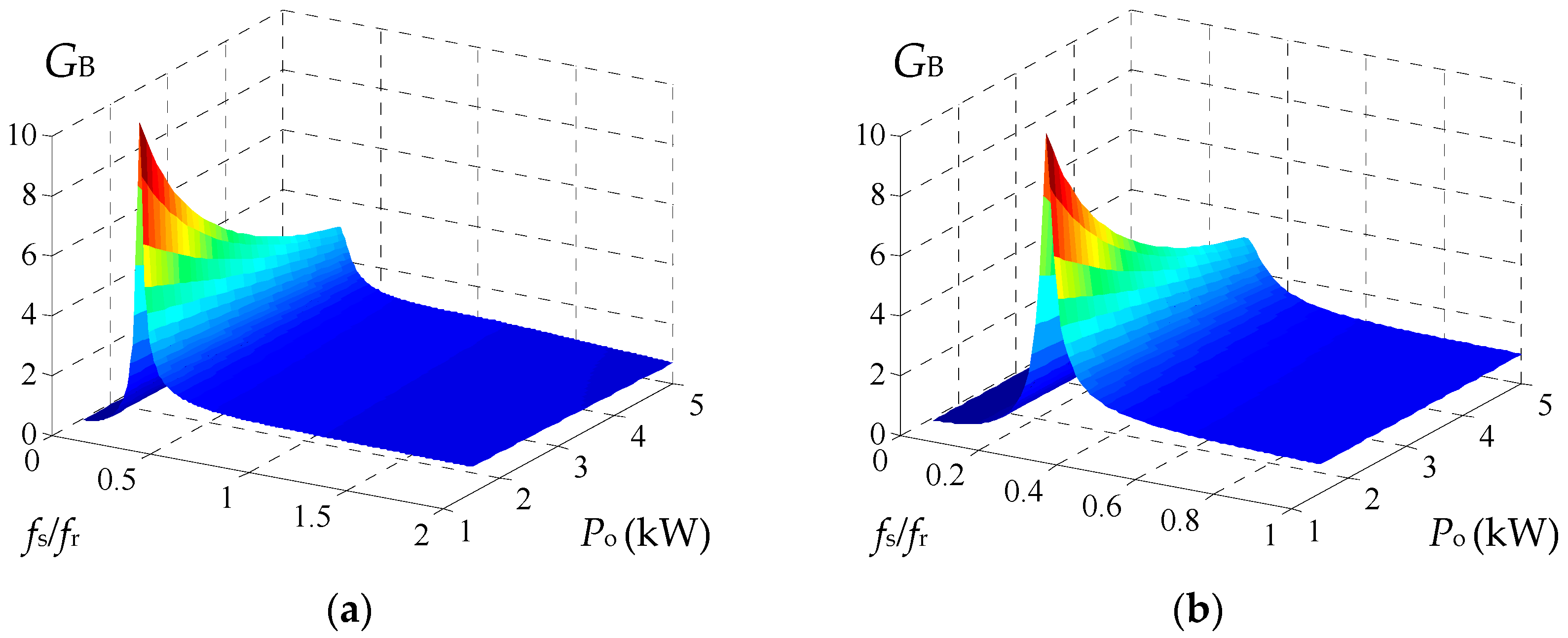
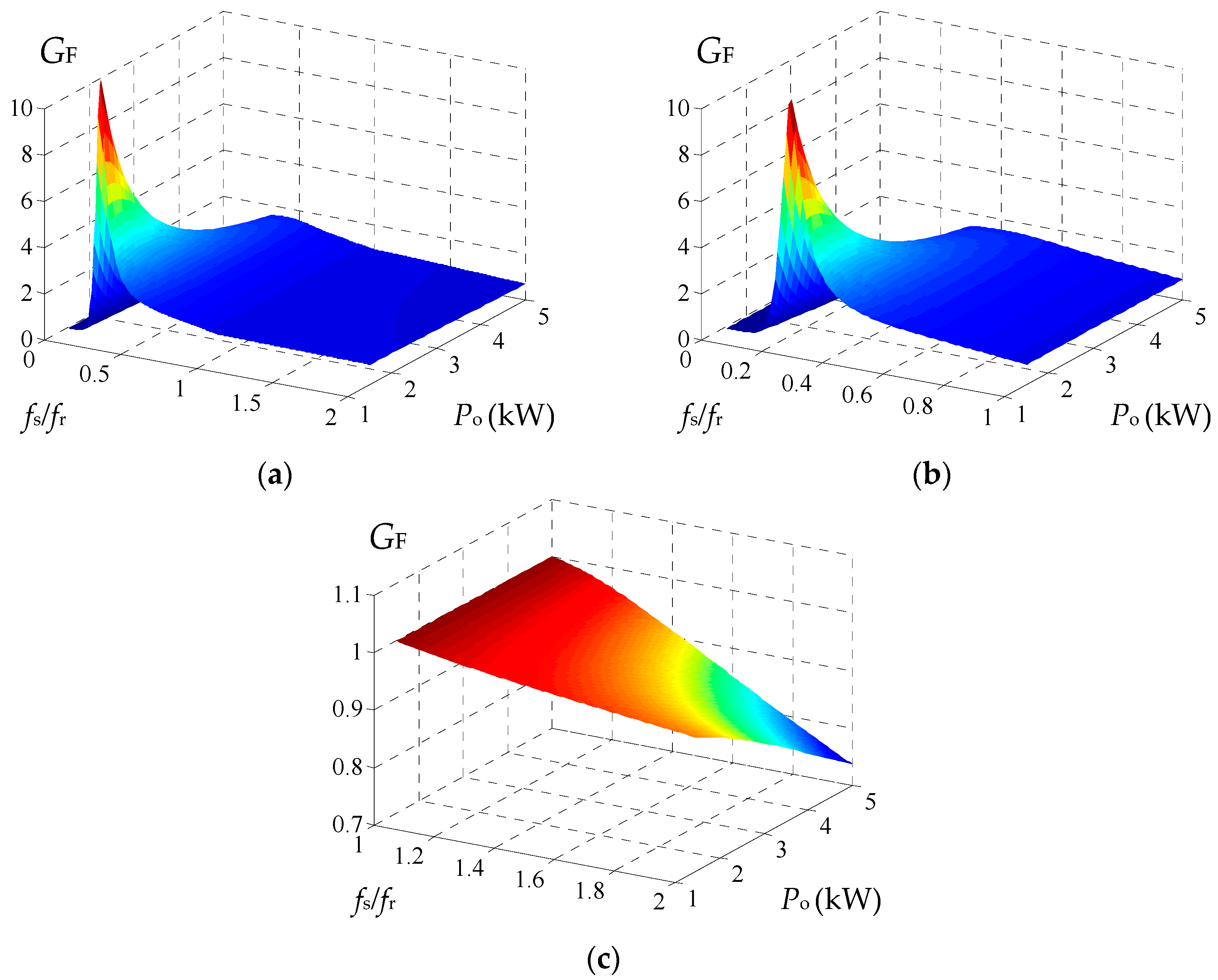
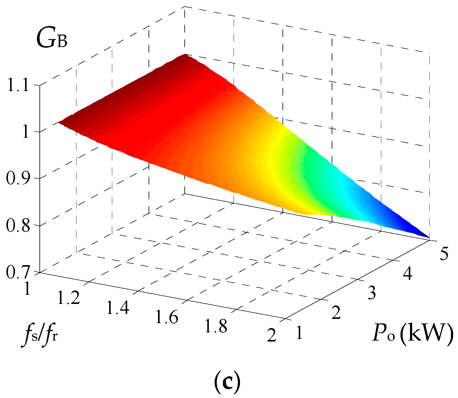
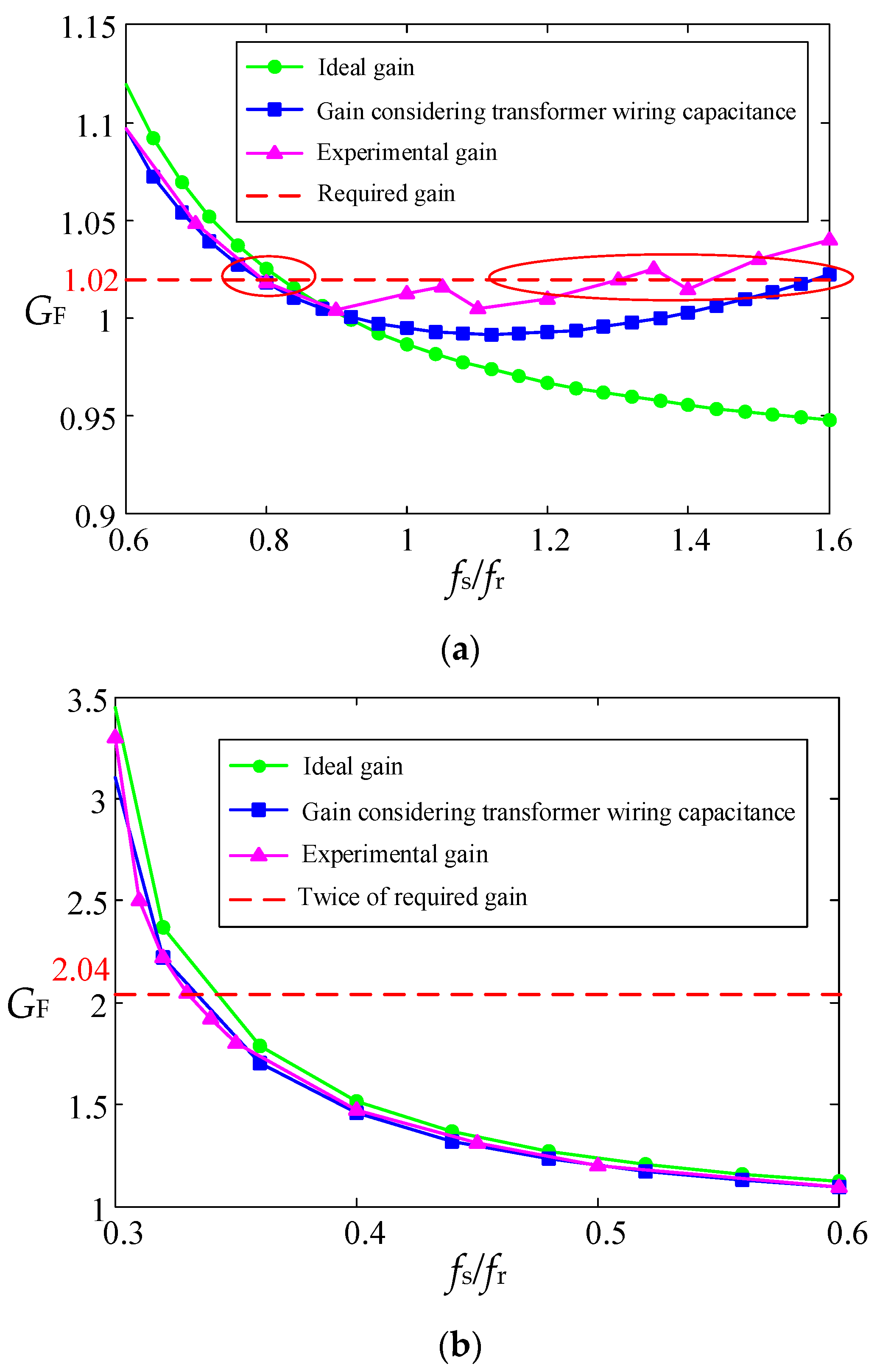
3.3. Load and Working Frquency Range

The peak gain should be larger than the required gain, Gr. It is because if the peak gain is smaller than Gr, Gr cannot be tracked. Taking a margin of 0.05Gr into consideration, the DC output resistance in half-bridge configuration, Ro,H, should satisfy the following equation:
G F , H ( f H , 1 , R o , H ) 1.05 G r
In (8), GF,H is the voltage gain of half-bridge CLTC, fH,1 is the maximum point.
Also, Ro,H should be bigger than twice of the rated resistance, Ro,H,rated, in full-bridge. As Section 3.2 tells, the selection of Ro,H should guarantee that the current stresses in half-bridge are no bigger than those in full-bridge. Thus:
R o , H 2 R o , F , rated
The working frequency of CLTC in half-bridge configuration, should be in the range of [fH,1,max, fr]. The working frequency should be lower than fr to avoid upturn phenomenon of gain curve. Also, when load is heavier in half-bridge, fH,1 gets larger as Figure 8 shows, so the lower limit of the working frequency is the largest value of fH,1, fH,1,max. In the range of [fH,1,max, fr], the gain curve monotonously declines with working frequency, and the slope is sharper in half-bridge configuration. It is ideal for voltage regulation of CLTC.

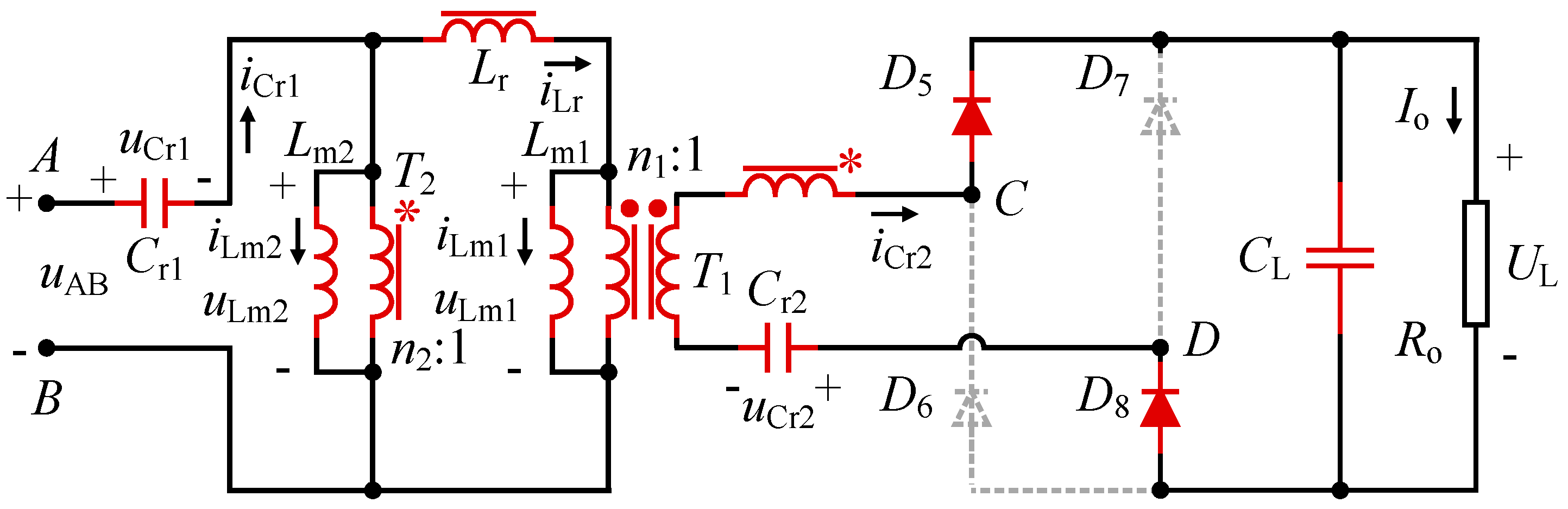
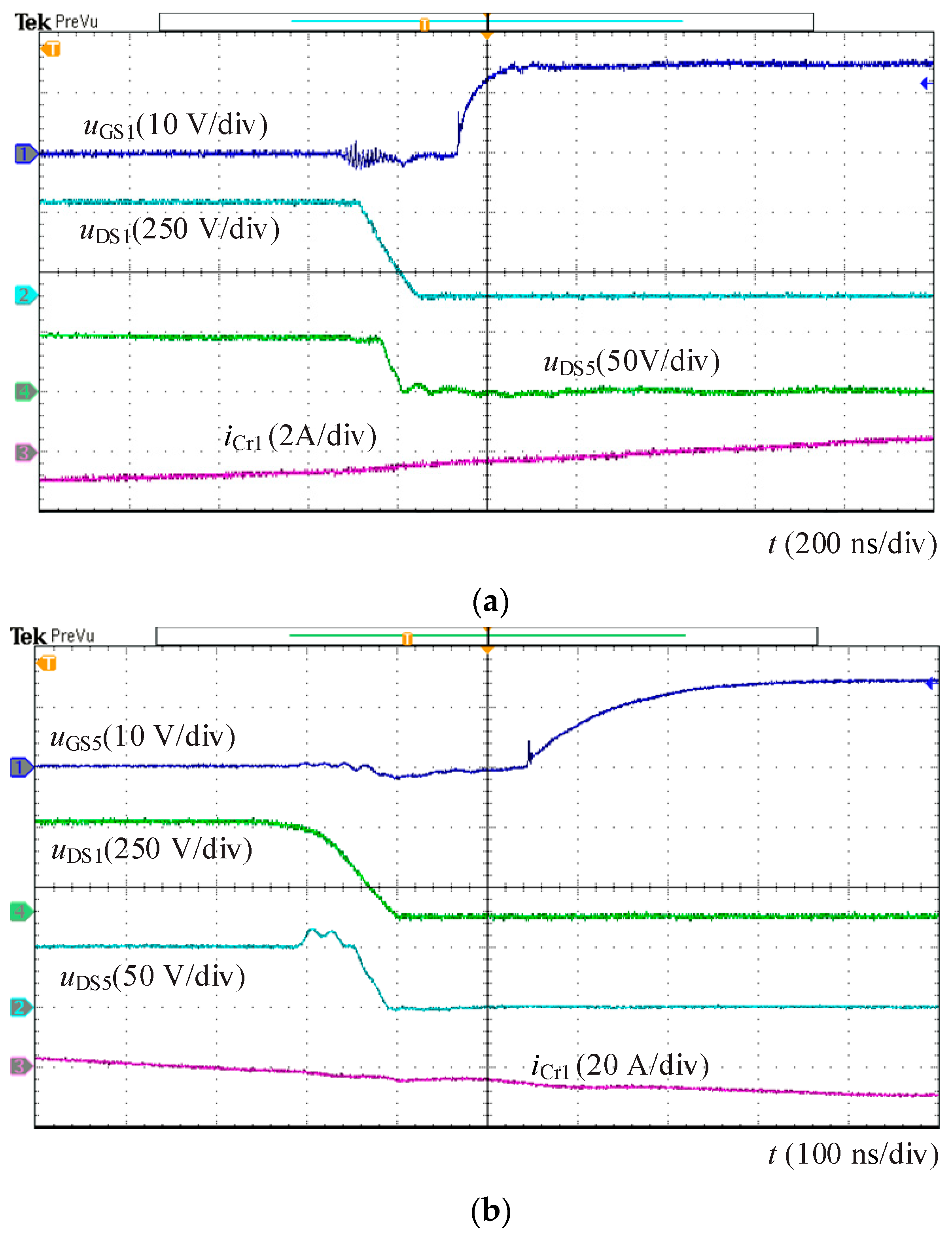
4. Synchronous Rectification Strategy Based on Estimation of Body Diodes’ Conduction Time

In consideration of improving the efficiency, a digital synchronous rectification strategy is proposed in forward mode. No auxiliary circuit is added. The proposed strategy adjusts conduction time of switches in LVS by calculating rectifier diodes’ conduction time in half period, tSR. A whole process of calculating tSR is proposed and verified in this section. It can be used in both full-bridge configuration and half-bridge configuration.

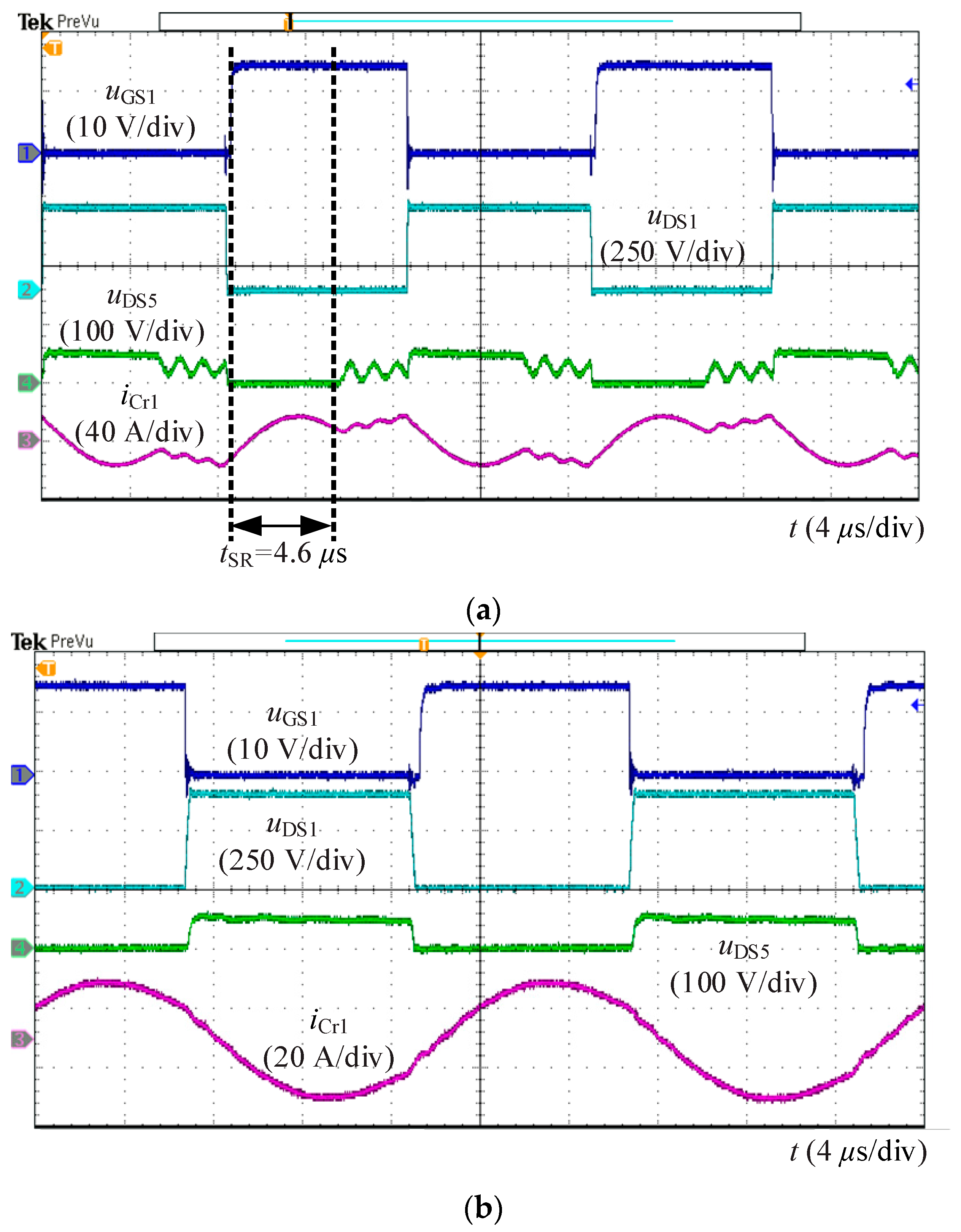
4.1. Synchornous Rectification Strategy

With the proposed digital synchronous rectification strategy, all the driving signals of HVS switches S1–S4 and LVS SR switches S5–S8 are given by STM32F series chip. The turn-on time of SR switches is set to the same with HVS main switches. But the conduction time (the interval between turn-on and turn-off time) is set with the estimation value of body diodes’ conduction time in half period, tSR, so tSR should be calculated for synchronous rectification.

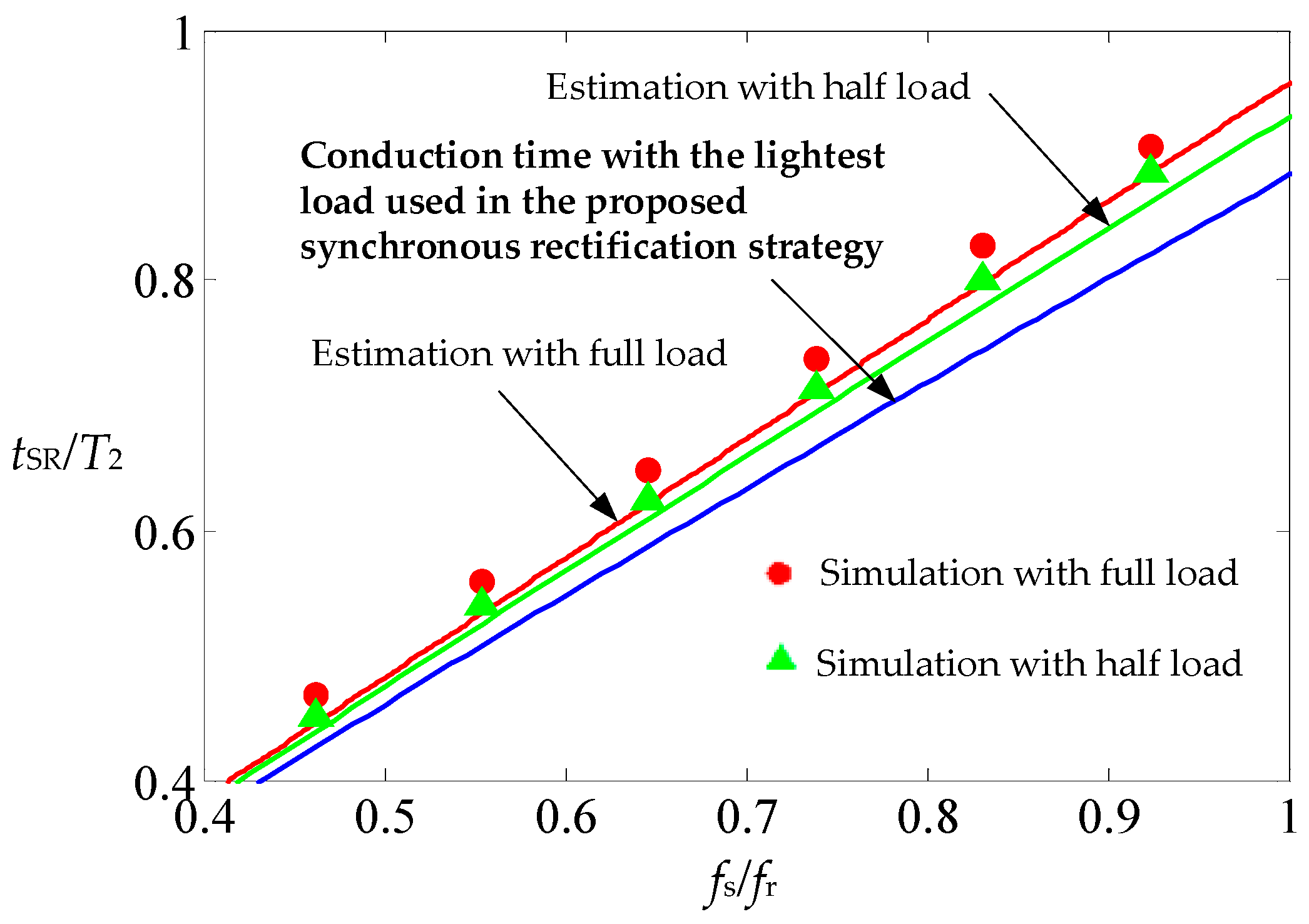
4.2. Estimation of the Body Diodes’ Conduction Time

When working frequency of CLTC is larger than main resonant frequency, tSR is half working period because the secondary resonance doesn’t exist. However, when working frequency is smaller than main resonant frequency, tSR is a variable with respect to Ro and fs. So discussion is focused on tSR when working frequency is smaller than main resonant frequency.
In Figure 9, assuming resonant current on LVS, iCr2, is approximated to a sinusoidal pulse:
i Cr 2 = { I Cr 2 sin ( π × t t SR ) , 0 t t SR 0 , t SR t T
ICr2 is the peak value of iCr2, t is the real time, T2 is half period, 1/(2fs). The value of uAB is UH in this period.
By using the law of conservation of electric charge, it can be obtained that:
0 t SR I Cr 2 sin ( π × t t SR ) d t = I o × T 2
According to (13), ICr2 can be expressed by:
I Cr 2 = I o π T 2 2 t SR
The voltage of Cr2 can be expressed by:
u Cr 2 ( t ) = 1 C r 2 0 t I Cr 2 sin ( π × t t SR ) d t + U Cr 2 , 0
As iCr2 is 0 and the voltage of Cr2 stays the same during tSRT2, the following equation is found:
U Cr 2 , 0 = u Cr 2 ( T 2 ) = u Cr 2 ( t SR )
Applying (15) into (16), the UCr2,0 can be expressed by:
U Cr 2 , 0 = t SR 2 U L 2 C r 2 T 2 R o
The voltage of magnetizing inductance Lm1 and Lm2, uLm1 and uLm2, can form following equations:
{ u Lm 1 ( t ) n 1 + u Lm 2 ( t ) n 2 = U L + U Cr 2 ( t ) ( 1 + L r L m 1 ) u Lm 1 ( t ) + 1 n 1 L r d i Cr 2 ( t ) d t = u Lm 2 ( t )
so uLm2 can be expressed by:
u Lm 2 ( t ) = n 2 n 1 L r d i Cr 2 ( t ) d t + ( 1 + L r L m 1 ) n 1 n 2 [ U L + U Cr 2 ( t ) ] n 2 + n 1 ( 1 + L r L m 1 )
The instantaneous voltage between HVS full-bridge legs, uAB, can be expressed as:
u AB ( t ) = U C r 1 , 0 + 1 C r 1 0 t i Cr 1 ( t ) d t + u Lm 2 ( t )
where, UCr1,0 is the initial voltage of resonant capacitor Cr1 at t0, and the instantaneous current of Cr1, iCr1, can be expressed as:
i Cr 1 ( t ) = i Lm 1 ( t ) + i Lm 2 ( t ) + ( 1 n 1 + 1 n 2 ) i Cr 2 ( t )
In order to simplify calculation process, Lm2 is supposed to be subject to uAB during 0–tSR. So iLm2 and iLm1 can be expressed as linearly increasing currents:
i Lm 1 ( t ) = U H 2 ( L m 1 + L r ) t + I Lm 1 , 0
i Lm 2 ( t ) = U H 2 L m 2 t + I Lm 2 , 0
ILm1,0 and ILm2,0 is the initial value of ILm1 and ILm2:
I Lm 1 , 0 = U H × t SR 4 ( L m 1 + L r )
I Lm 2 , 0 = U H × t SR 4 L m 2
Realizing that uAB(t) = UH and substituting (19) and (21) into (20), gives:
U H = U Cr 1 , 0 + 1 C r 1 0 t [ i Lm 1 ( t ) + i Lm 2 ( t ) + ( 1 n 1 + 1 n 2 ) i Cr 2 ( t ) ] d t + n 2 n 1 L r d i Cr 2 ( t ) d t + ( 1 + L r L m 1 ) n 1 n 2 [ U L + U Cr 2 ( t ) ] n 2 + n 1 ( 1 + L r L m 1 )
Getting the derivative of the above equation:
0 = D π 2 t SR 2 sin ( π × t t SR ) + E × sin ( π × t t SR ) + F × t SR × t + I Lm 1 , 0 + I Lm 2 , 0 I Cr 2
In (27), D, E, F are:
D = C r 1 n 2 L r n 1 [ n 2 + n 1 ( 1 + L r L m 1 ) ]
E = C r 1 ( 1 + L r L m 1 ) n 1 n 2 C r 2 [ n 2 + n 1 ( 1 + L r L m 1 ) ] + 1 n 1 + 1 n 2
F = [ 1 2 ( L m 1 + L r ) + 1 2 L m 2 ] U H I Cr 2 t SR
UH can be expressed as UL/MSD, so F can be simplified by:
F = [ 1 2 ( L m 1 + L r ) + 1 2 L m 2 ] 2 R o π T 2 M SD
I Lm 1 , 0 + I Lm 2 , 0 I Cr 2 is close to 0 as ICr2 is much larger than ILm1,0 + ILm2,0. When t is close to 0, π × t t SR sin ( π × t t SR ) , tSR is the solution of (27):
t SR = π E + π E 2 + 4 D F π 2 F
In Figure 10, the normalized estimated conduction time tSR/T2 versus normalized operating frequency fs/fr and different load (dots—simulation, solid lines—theoretical prediction). Figure 10 reveals good agreement between theoretical values and simulation results. The curve of tSR/T2 is basically proportional to fs/fr, and grows with the increase of load.
Based on the above analysis, the conduction time of LVS switches is set to estimated conduction time tSR obtained when load is the lightest, so the conduction time of LVS switches in the proposed synchronous rectification strategy is not relevant to the load. It is a parameter changing with operating frequency. LVS switches turn on firstly to reduce conduction loss. Then, as estimated conduction time tSR is a little smaller than the real conduction time of LVS body diodes, the body diodes of LVS switches conduct until the LVS resonant current becomes zero. Efficiency is not affected because the duration when body diodes conduct is short. The proposed digital synchronous rectification strategy is simple and effective, the effects are discussed in sections below.

5. Power Loss Analysis

The power loss of converters is the key factor for component selection and design. In this section, the power loss distribution is calculated with mathematical models and compared with different LVS DC voltages. The HVS DC voltage of the converter stays the same. The power loss with half-bridge configuration and synchronous rectification strategy are discussed in this section, too.
Before further analysis, several parameters are defined as follows, PHSW,off is the turn-off loss of HVS power switches, PHSW,con is the conduction loss of HVS power switches, PLSW,off is the turn-off loss of LVS power switches, PLSW,con is the conduction loss of LVS power switches, PL is the power loss of resonant inductor, PT,Σ is the total power loss of transformers, PWIRE,con is the conduction loss in printed circuit board and copper bar, PHD is the power loss of HVS diodes, PLD is the power loss of LVS body diodes in power switches.

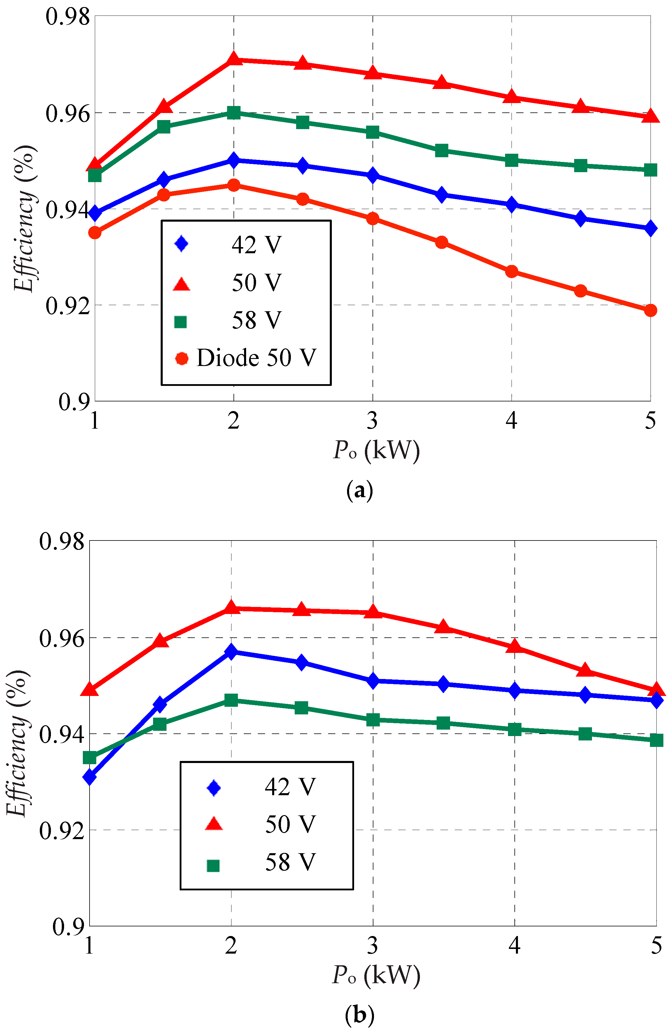
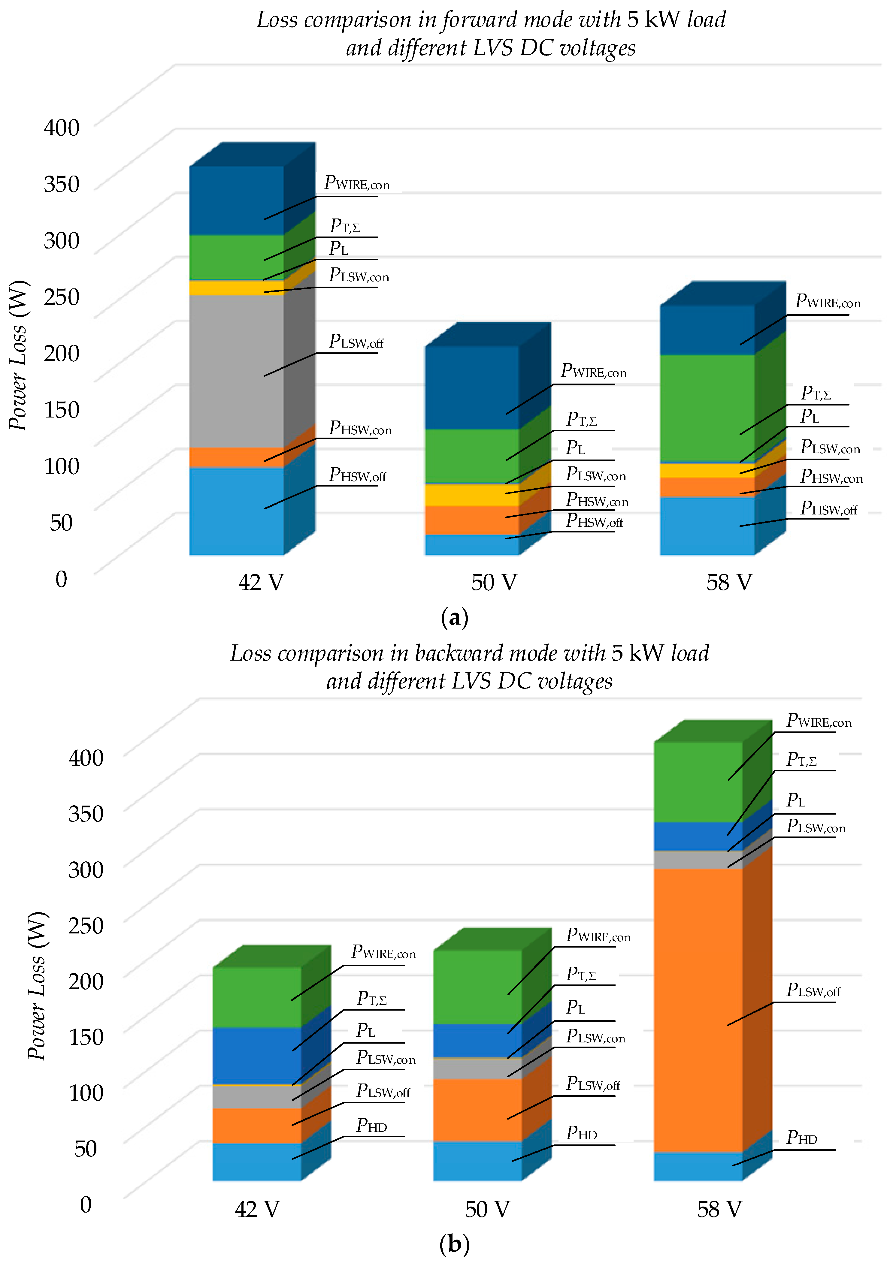
5.1. Loss Distribution with Different LVS DC Voltages

Power loss distribution with 5 kW load in forward and backward mode is shown in Figure 11. The power loss distribution is conducted with three LVS DC voltages of 42, 50 and 58 V and the HVS voltage of 400 V. In forward mode, the column of “50 V” is obtained around main resonant frequency, while the column of “42 V” is obtained with higher frequency and column of “58 V” is obtained with lower frequency. In backward mode, the column of “50 V” is obtained around main resonant frequency, while the column of “42 V” is obtained with lower frequency and column of “58 V” is obtained with higher frequency.
PHSW,off and PLSW,off are the dominant power losses. PL and PT,Σ change little with the change of LVS DC voltage. PWIRE,con is large due to proximity effect and skin effect. The column of “42 V” in forward mode and the column of “58 V” in backward mode have greater power loss compared to the other columns. This is mainly because PHSW,off and PLSW,off are larger due to larger turn-off currents and higher working frequencies. The HVS switches are SiC power devices, and the LVS switches are Si power devices. Compared to LVS switches, the HVS switches have less turn-off delay time and fall time. So the switching loss of LVS switches is larger than that of HVS switches. Thus, the efficiency in forward mode is higher than that in backward mode in general.

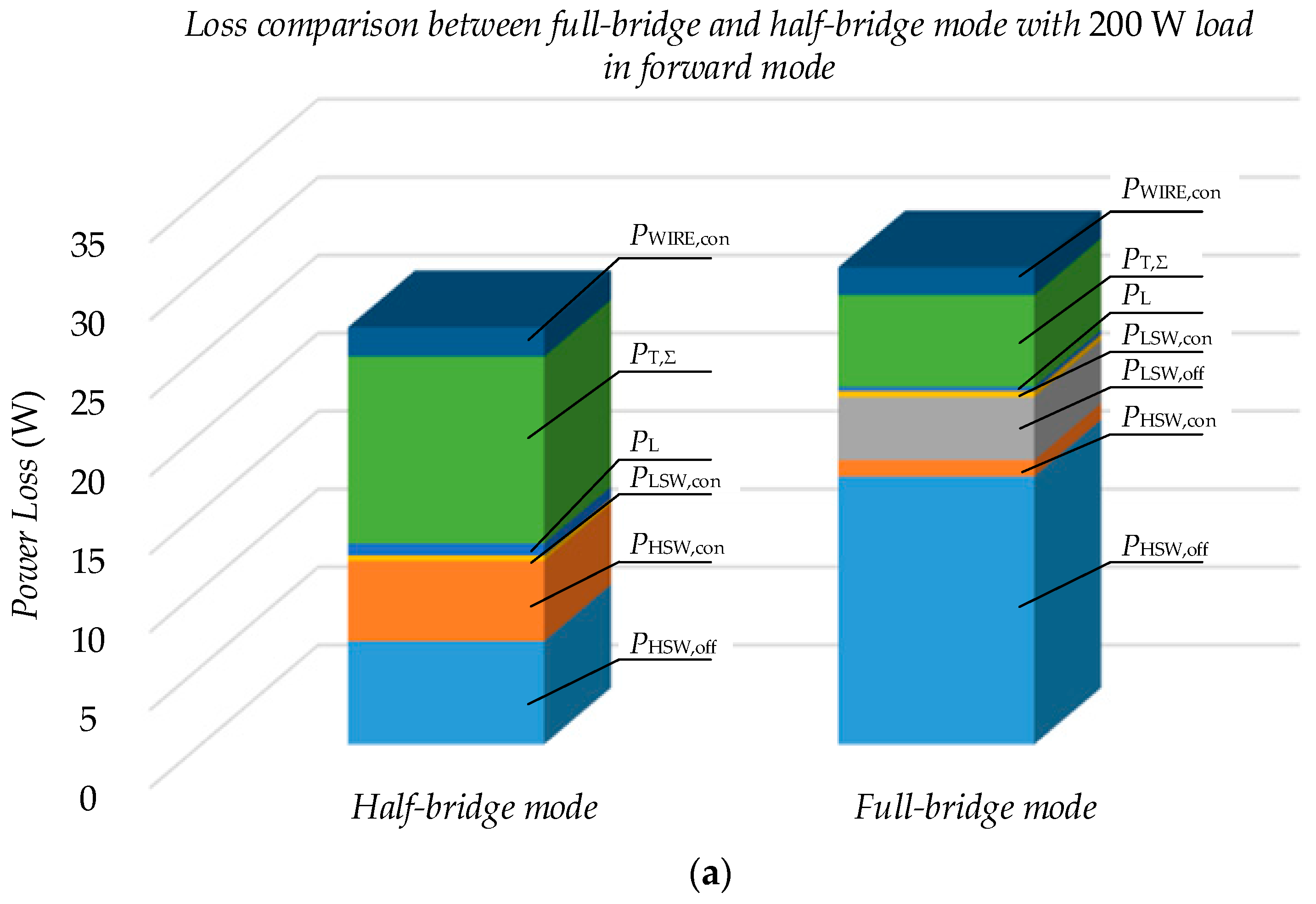
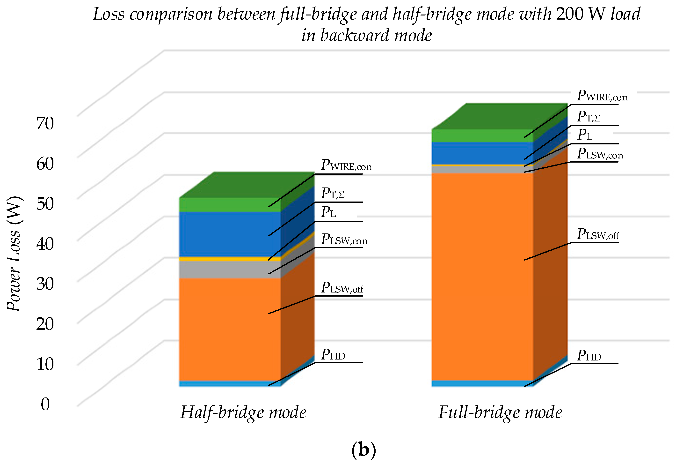
5.2. Power Loss Distribution and Comparison between Full-Bridge and Half-Bridge Configuration

The power loss distribution and comparison between full-bridge and half-bridge configuration is made to demonstrate the advantage of half-bridge configuration in efficiency. Taking forward mode for example, changing from full-bridge configuration to half-bridge configuration has impacts as follows:
(1)
PHSW,off and PLSW,off decrease largely. In forward mode, switches staying on on-off mode in HVS decrease from 4 to 2, and their working frequency decreases from 160 kHz to around 40 kHz. So PHSW,off decreases largely with half-bridge configuration. Also, PLSW,off decreases with less turn-off current and lower working frequency.
(2)
The conduction loss of all devices increases. Resonant current on HVS increases to about twice, so PHSW,con, conduction loss of resonant inductor and primary windings of transformers are amplified. However, as resonant current on LVS changes little, PLSW,con and the conduction loss of secondary windings in transformers stay the same.
(3)
Core loss of resonant inductor and transformers stays the same. In half-bridge LLC, working frequency fs decreases. However, Bmax, the peak flux density, increases because peak value of current increases. With Steinmetz’s equation Pcore = KfsαBmaxβVe, the core losses of resonant inductor and transformers in half-bridge configuration change little.
Figure 12a shows power loss distribution and comparison with load of 200 W in forward mode. Efficiencies of half-bridge and full-bridge configuration are 87.7% and 86.7%. The power loss distribution is in accordance with the above analysis. Compared to full-bridge configuration, efficiency is a little higher in half-bridge configuration.
Figure 12b shows power loss distribution and comparison with load of 200 W in backward mode. PLSW,off gets much smaller in half-bridge configuration. The power loss is cut down by 26.7% and the efficiency is 81.5% in half-bridge configuration.

5.3. Power Loss Distribution and Comparison with and without Synchronous Strategy

Figure 13 shows the power loss distribution and comparison with and without synchronous strategy. When body diodes of LVS switches are used to realize rectification, PLD is quite large with diode forward voltage of 0.9 V. However, the drain-source on-state resistance of LVS switches is only 0.7 mΩ. Thus, with the use of the proposed synchronous strategy, PLSW,con is quite small. The total loss is cut by 49% with the use of synchronous strategy, showing the advantage in power loss reduction and efficiency enhancement.

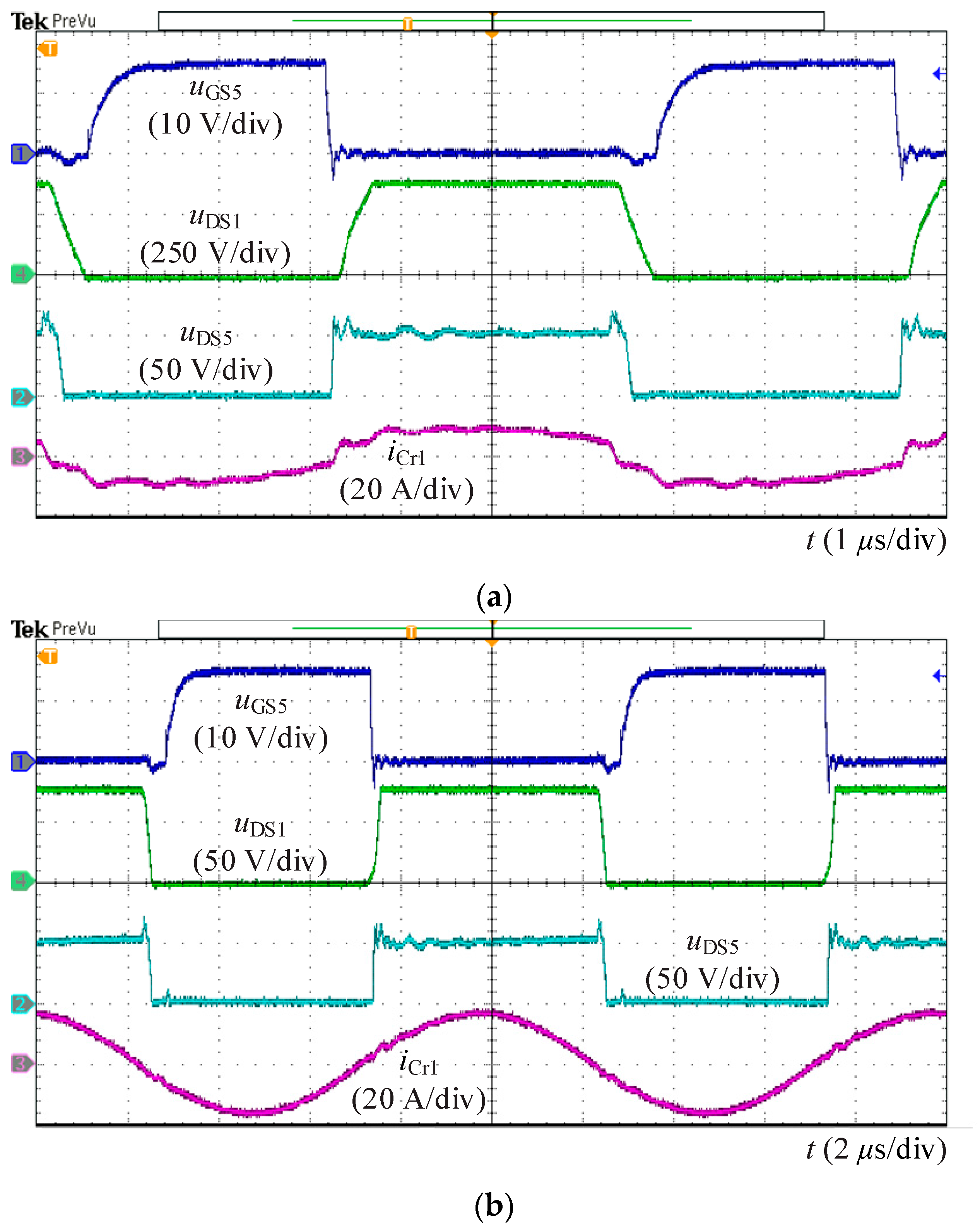
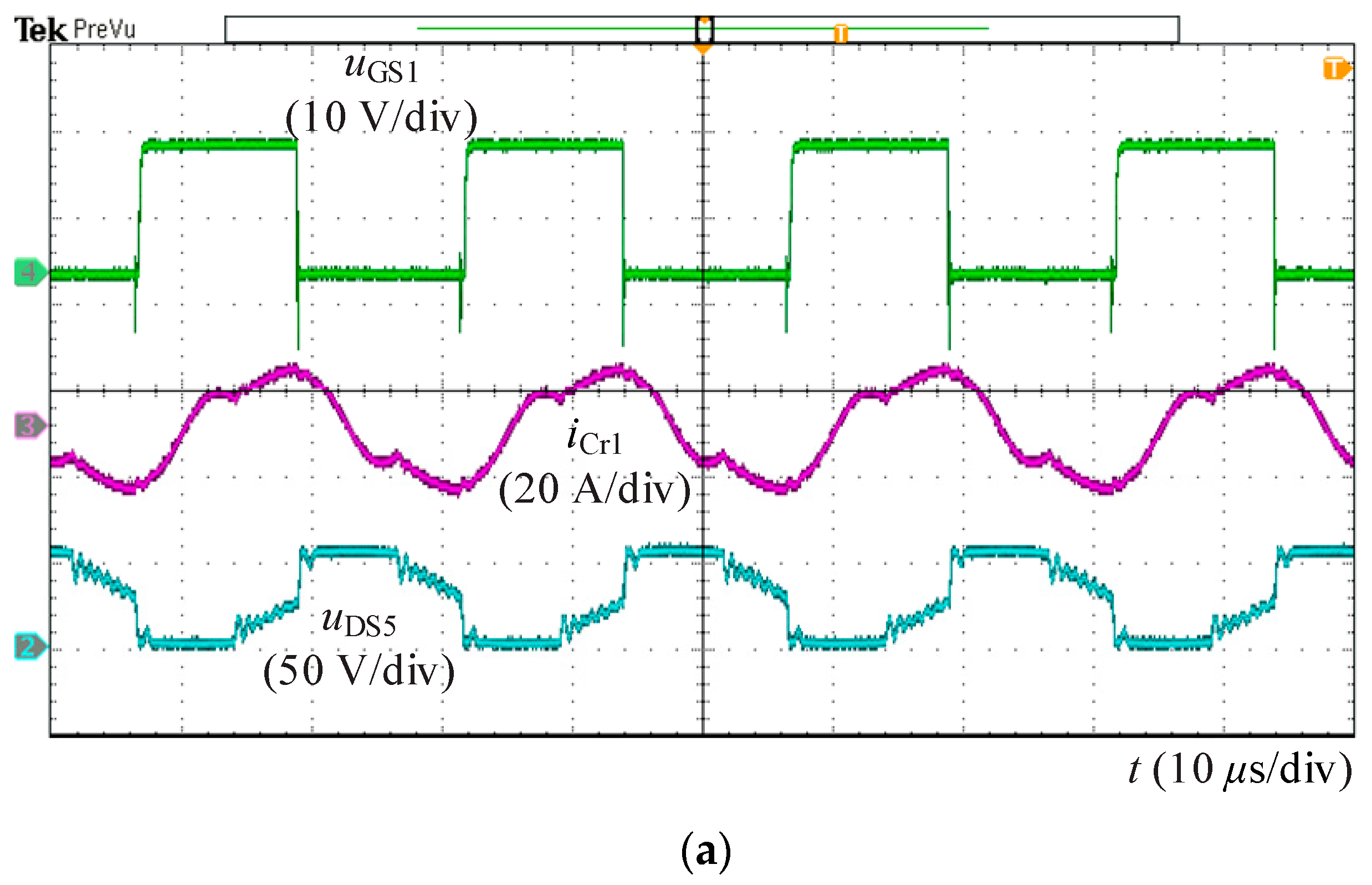
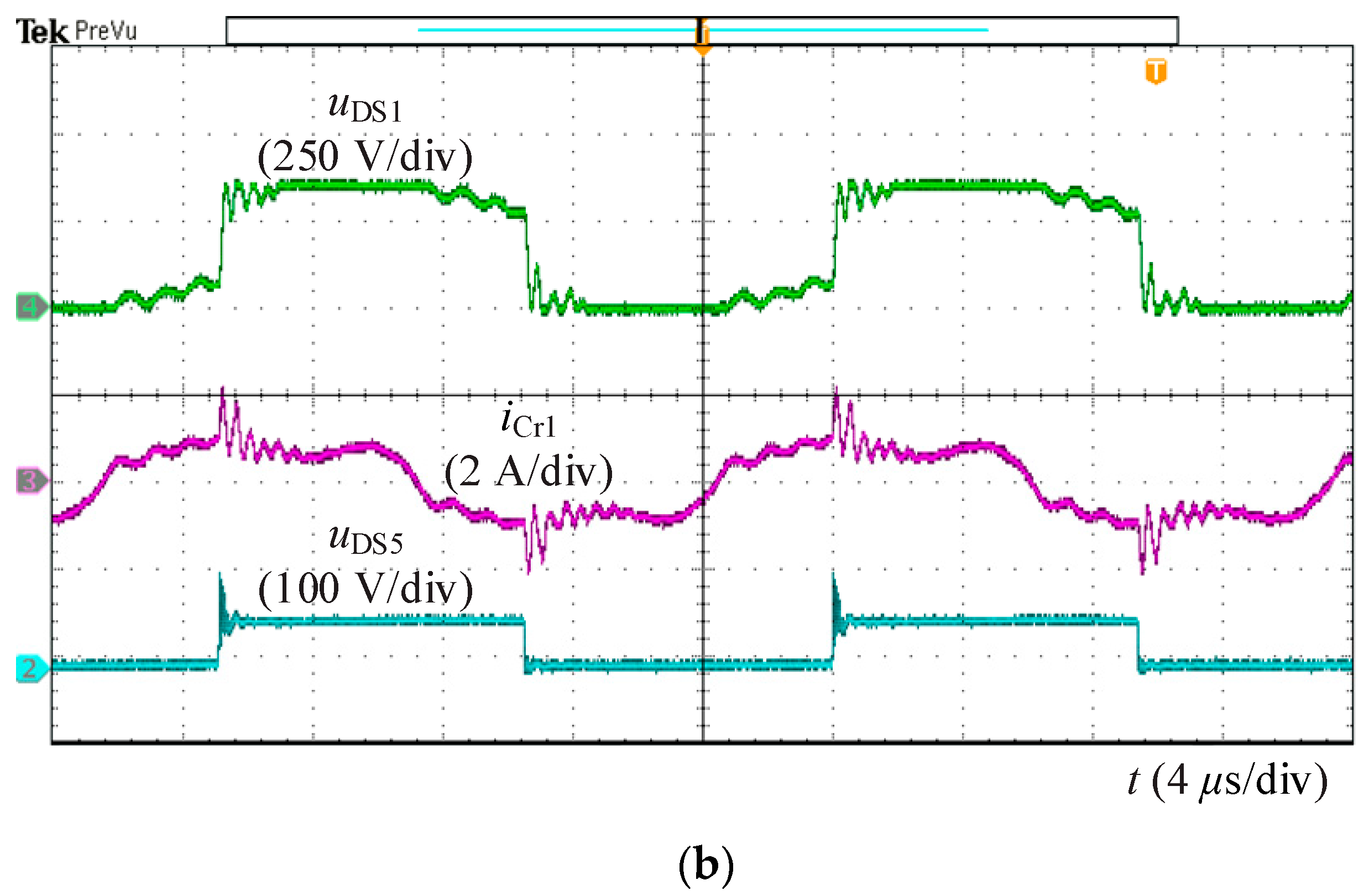
6. Experimental Results

A 5 kW prototype is built in the laboratory to verify the above analysis. The parameters of the components are listed in Table 1.
Figure 14 shows that ZVS of power switches can be realized in both forward and backward modes. In forward mode, the D-S voltage of S1 decreases to 0, before the driving signal of S1 comes. In backward mode, the D-S voltage of S5 decreases to 0, before the driving signal of S5 comes. The dead time of 200 ns is wide enough for both HVS and LVS power switches, while the efficiency is not greatly reduced.
Figure 15 shows experiment results in forward mode. The tSR is 4.6 μs in Figure 15a with working frequency of 60 kHz and load of 3.5 kW. The tSR is 4.5 μs with Equation (25) and 4.3 μs in the proposed synchronous rectification strategy, which is basically consistent with the experiment results. The accuracy of calculation and the effectiveness of proposed synchronous rectification strategy are verified through experiments. Figure 15b shows the waveforms around main resonant frequency. The resonant current is quite close to sinusoidal wave. The power loss is lower because of smaller turn-off loss in this situation.
Figure 16 shows experiment results in backward mode. In Figure 16a, secondary resonance does not happen, so ZCS of HVS diodes cannot be realized. In Figure 16b, the resonant current is quite close to sinusoidal wave around main resonant frequency. The power loss in Figure 16b is lower because of smaller turn-off loss.
Experiments are conducted to verify the effectiveness of half-bridge configuration at light load condition in Figure 17. In both forward and backward mode, the adoption of half-bridge configuration can track a gain of 1.02. Compared to full-bridge, the fall of working frequency in half-bridge configuration reduces turn-off loss, which is very good for efficiency.
Efficiency comparison is conducted with experiments at light load condition. In Table 2, the efficiency in half-bridge configuration is higher than that in full-bridge, which is in accord with analysis in Section 5.2. The advantage of half-bridge configuration is verified through experiments.
Efficiencies of the proposed converter with different loads and LVS DC voltages are measured and plotted in Figure 18. The efficiency with 5 kW load and 50 V LVS DC voltage is 95.9% and 94.9% in forward and backward mode. The maximum efficiency of the converter is 97.0%, with load of 2 kW and LVS DC voltage of 50 V in forward mode. Due to less turn-off currents and lower working frequencies, the efficiency of “58 V” or “50 V” is higher than that of “42 V” in forward mode and the efficiency of “42 V” or “50 V” is higher than that of “58 V” in backward mode. It is in accord with theoretical analysis in Section 5. High efficiency can be achieved in a wide load range. Even with 1 kW load, the efficiency is still over 92% due to the wide ZVS soft switching operation range and little turn-off currents.
The comparative experiments are conducted with and without synchronous rectification strategy when LVS DC voltage is 50 V, displayed as “50 V” and “Diode 50 V”. From the converter power loss distribution, the LVS diode conduction loss is the dominant part in “Diode 50 V”, which occupies nearly 50% of the total power loss. Experiment results show that the efficiency is improved largely with the help of the proposed synchronous rectification strategy.

7. Conclusions

In this work, a new CLTC multi-resonant DC-DC converter is proposed. Possessing the optimal ZVS + ZCS soft switching feature in all load range, CLTC benefits from little turn-off loss and high efficiency. The gain range is so wide that the demands of applications like battery chargers and DC microgrids can be satisfied easily. The problem of voltage regulation under light load conditions is so serious that voltage is not controllable. The hybrid full-bridge/half-bridge configuration is proposed to make gain curve monotonous under light load conditions. Discussion about voltage and current stresses, load and working frequency range in half-bridge configuration are put forth as well. Besides, a digital synchronous rectification strategy is proposed in forward mode to improve the working efficiency. The turn-on time of LVS switches is set to the same as the HVS switches. The conduction time of LVS switches equals the estimation value of body diodes’ conduction time with the lightest load. Simulations verify the accuracy of this estimation. Furthermore, power loss analysis is conducted with different LVS DC voltages in two directions. Power loss is much more when the working frequency is beyond main resonant frequency, because of high conduction losses and turn-off losses. Efficiency with a half-bridge configuration is a little higher than that with full-bridge configuration in both directions, due to less turn-off losses. The loss is cut by 49% with the use of a synchronous strategy, showing the advantage in improving efficiency. At last, experiments are conducted to validate the theoretical analysis above. ZVS feature, the effectiveness of hybrid full-bridge/half-bridge configuration, and the validity of proposed digital synchronous rectification strategy are all verified through experiments. With the help of ZVS + ZCS feature, high efficiency can be harvested in a wide load range. The full load efficiency is 95.9% in forward mode and 94.9% in backward mode with LVS DC voltage of 50 V. The maximum efficiency is 97.0% with a LVS DC voltage of 50 V and load of 2 kW.

Acknowledgments

This research was supported by the National High Technology Research and Development Program (863 Program) of China (Grant: 2015AA050603). The authors would also like to thank the anonymous reviewers for their valuable comments and suggestions to improve the quality of the paper.

Author Contributions

Shu-huai Zhang, Yi-feng Wang, Bo Chen designed the main parts of the study, including hybrid full-bridge/half-bridge configuration, synchronous rectification strategy loss model, power loss analysis and experiments. Yi-feng Wang is also responsible for writing and revising the paper. Fu-qiang Han and Qing-cui Wang helped in the hardware development.

Conflicts of Interest

The authors declare no conflict of interest.

References

  1. Fang, Z.; Wang, J.; Duan, S.; Shao, J.; Hu, G. Stability Analysis and Trigger Control of LLC Resonant Converter for a Wide Operational Range. Energies 2017, 10, 1448. [Google Scholar] [CrossRef]
  2. Wang, C.; Li, W.; Wang, Y.; Han, F.; Meng, Z.; Li, G. An Isolated Three-Port Bidirectional DC-DC Converter with Enlarged ZVS Region for HESS Applications in DC Microgrids. Energies 2017, 10, 446. [Google Scholar] [CrossRef]
  3. Wang, C.; Li, W.; Wang, Y.; Han, F.; Chen, B. A High-Efficiency Isolated LCLC Multi-Resonant Three-Port Bidirectional DC-DC Converter. Energies 2017, 10, 934. [Google Scholar] [CrossRef]
  4. Chen, B.; Wang, P.; Wang, Y.; Li, W.; Han, F.; Zhang, S. Comparative Analysis and Optimization of Power Loss Based on the Isolated Series/Multi Resonant Three-Port Bidirectional DC-DC Converter. Energies 2017, 10, 1565. [Google Scholar] [CrossRef]
  5. Twiname, R.P.; Thrimawithana, D.J.; Madawala, U.K.; Baguley, C.A. A New Resonant Bidirectional DC–DC Converter Topology. IEEE Trans. Power Electron. 2014, 29, 4733–4740. [Google Scholar] [CrossRef]
  6. Wu, H.; Ding, S.; Sun, K.; Zhang, L.; Li, Y.; Xing, Y. Bidirectional Soft-Switching Series-Resonant Converter With Simple PWM Control and Load-Independent Voltage-Gain Characteristics for Energy Storage System in DC Microgrids. IEEE Trans. Power Electron. 2013, 28, 995–1007. [Google Scholar] [CrossRef]
  7. Park, J.; Choi, S. Design and Control of a Bidirectional Resonant DC–DC Converter for Automotive Engine/Battery Hybrid Power Generators. IEEE Trans. Power Electron. 2014, 29, 3748–3757. [Google Scholar] [CrossRef]
  8. Shen, Y.; Wang, H.; Al-Durra, A.; Qin, Z.; Blaabjerg, F. A Fixed-Frequency Bidirectional Resonant DC-DC Converter Suitable for Wide Voltage Gain Range. IEEE Trans. Power Electron. 2017, 99, 1–19. [Google Scholar]
  9. Hu, S.; Deng, J.; Mi, C.; Zhang, M. Optimal design of line level control resonant converters in plug-in hybrid electric vehicle battery chargers. IET Electron. Syst. Transp. 2013, 4, 21–28. [Google Scholar] [CrossRef]
  10. Tan, X.; Ruan, X. Equivalence relations of resonant tanks: A new perspective for selection and design of resonant converters. IEEE Trans. Ind. Electron. 2016, 63, 2111–2123. [Google Scholar] [CrossRef]
  11. Corradini, L.; Seltzer, D.; Bloomquist, D.; Zane, R.; Maksimović, D.; Jacobson, B. Minimum Current Operation of Bidirectional Dual-Bridge Series Resonant DC/DC Converters. IEEE Trans. Power Electron. 2012, 27, 3266–3276. [Google Scholar] [CrossRef]
  12. Ibanez, F.; Echeverria, J.; Vadillo, J.; Fontan, L. State-Plane Analysis of Anomalous Step-Up Behavior in Series-Resonant Converters. IEEE J. Emerg. Sel. Top. Power Electron. 2016, 4, 1026–1035. [Google Scholar] [CrossRef]
  13. Li, X.; Bhat, A. Analysis and Design of High-Frequency Isolated Dual-Bridge Series Resonant DC/DC Converter. IEEE Trans. Power Electron. 2010, 25, 850–862. [Google Scholar]
  14. Ibanez, F.; Echeverria, J.; Fontan, L. Novel technique for bidirectional series-resonant DC/DC converter in discontinuous mode. IET Power Electron. 2013, 6, 1019–1028. [Google Scholar] [CrossRef]
  15. Ibanez, F.; Echeverria, J.; Vadillo, J.; Fontan, L. Frequency response analysis for bidirectional series resonant DC/DC converter in discontinuous mode. IET Power Electron. 2014, 7, 2374–2386. [Google Scholar] [CrossRef]
  16. Ibanez, F.; Echeverria, J.; Vadillo, J.; Fontan, L. A Step-Up Bidirectional Series Resonant DC/DC Converter Using a Continuous Current Mode. IEEE Trans. Power Electron. 2015, 30, 1393–1402. [Google Scholar] [CrossRef]
  17. Jiang, T.; Zhang, J.; Wu, X.; Sheng, K.; Wang, Y. A Bidirectional Three-Level LLC Resonant Converter with PWAM Control. IEEE Trans. Power Electron. 2016, 31, 2213–2225. [Google Scholar] [CrossRef]
  18. Jiang, T.; Zhang, J.; Wu, X.; Sheng, K.; Wang, Y. A Bidirectional LLC Resonant Converter with Automatic Forward and Backward Mode Transition. IEEE Trans. Power Electron. 2015, 30, 757–770. [Google Scholar] [CrossRef]
  19. Jung, J.; Kim, H.; Ryu, M.; Baek, J. Design Methodology of Bidirectional CLLC Resonant Converter for High-Frequency Isolation of DC Distribution Systems. IEEE Trans. Power Electron. 2013, 28, 1741–1755. [Google Scholar] [CrossRef]
  20. Zahid, Z.; Dalala, Z.; Chen, R.; Chen, B.; Lai, J. Design of Bidirectional DC-DC Resonant Converter for Vehicle-to-Grid (V2G) Applications. IEEE Trans. Transp. Electr. 2015, 1, 232–244. [Google Scholar] [CrossRef]
  21. He, P.; Khaligh, A. Comprehensive Analyses and Comparison of 1 kW Isolated DC-DC Converters for Bidirectional EV Charging Systems. IEEE Trans. Transp. Electr. 2017, 3, 147–156. [Google Scholar] [CrossRef]
  22. Lee, B.H.; Kim, M.Y.; Kim, C.E.; Park, K.-B.; Moon, G.W. Analysis of LLC resonant converter considering effects of parasitic components. In Proceedings of the INTELEC 31st International Telecommunications Energy Conference, Incheon, Korea, 18–22 October 2009; pp. 1–6. [Google Scholar]
  23. Zhao, S.; Xu, J.; Trescases, O. Burst-Mode Resonant LLC Converter for an LED Luminaire With Integrated Visible Light Communication for Smart Buildings. IEEE Trans. Power Electron. 2014, 9, 4392–4402. [Google Scholar] [CrossRef]
  24. Musavi, F.; Craciun, M.; Gautam, D.; Eberle, W. Control Strategies for Wide Output Voltage Range LLC Resonant DC–DC Converters in Battery Chargers. IEEE Trans. Veh. Technol. 2014, 63, 1117–1125. [Google Scholar] [CrossRef]
  25. Cai, G.; Liu, D.; Liu, C.; Li, W.; Sun, J. A High-Frequency Isolation (HFI) Charging DC Port Combining a Front-End Three-Level Converter with a Back-End LLC Resonant Converter. Energies 2017, 10, 1462. [Google Scholar]
  26. Kim, J.; Kim, C.; Kim, J.; Lee, J.; Moon, G. Analysis on Load-Adaptive Phase-Shift Control for High Efficiency Full-Bridge LLC Resonant Converter Under Light-Load Conditions. IEEE Trans. Power Electron. 2016, 31, 4942–4955. [Google Scholar]
  27. Pan, H.; He, C.; Ajmal, F.; Chen, H.; Chen, G. Pulse-width modulation control strategy for high efficiency LLC resonant converter with light load applications. IET Power Electron. 2014, 7, 2887–2894. [Google Scholar] [CrossRef]
  28. Wang, H.; Li, Z. A PWM LLC Type Resonant Converter Adapted to Wide Output Range in PEV Charging Applications. IEEE Trans. Power Electron. 2017, 1, 1–10. [Google Scholar] [CrossRef]
  29. Kim, J.H.; Kim, C.E.; Kim, J.K.; Moon, G.W. Analysis for LLC resonant converter considering parasitic components at very light load condition. In Proceedings of the 8th International Conference on Power Electronics, Jeju, Korea, 30 May–3 June 2011; pp. 1863–1868. [Google Scholar]
  30. Yeon, C.; Kim, J.; Park, M.; Lee, L.; Moon, G. Improving the Light-Load Regulation Capability of LLC Series Resonant Converter Using Impedance Analysis. IEEE Trans. Power Electron. 2017, 32, 7056–7067. [Google Scholar] [CrossRef]
  31. Tsai, C.; Shen, C.; Su, J. A Power Supply System with ZVS and Current-Doubler Features for Hybrid Renewable Energy Conversion. Energies 2013, 6, 4859–4878. [Google Scholar] [CrossRef]
  32. Xu, W.; Chan, N.; Or, S.; Ho, S.; Chan, K. A New Control Method for a Bi-Directional Phase-Shift-Controlled DC-DC Converter with an Extended Load Range. Energies 2017, 10, 1532. [Google Scholar] [CrossRef]
  33. Joo, D.; Byun, J.; Lee, B.; Kim, J. Adaptive delay control for synchronous rectification phase-shifted full bridge converter with GaN HEMT. IEEE Trans. Power Electron. 2017, 53, 1541–1542. [Google Scholar] [CrossRef]
  34. Yang, H.; Liao, J.; Cheng, X. Zero-voltage-transition auxiliary circuit with dual resonant tank for DC–DC converters with synchronous rectification. IET Trans. Power Electron. 2017, 6, 1157–1164. [Google Scholar] [CrossRef]
  35. Fu, D.; Liu, Y.; Lee, F.; Xu, M. A Novel Driving Scheme for Synchronous Rectifiers in LLC Resonant Converters. IEEE Trans. Power Electron. 2009, 24, 1321–1329. [Google Scholar] [CrossRef]
  36. Zhang, J.; Wang, J.; Zhang, G.; Qian, Z. A Hybrid Driving Scheme for Full-Bridge Synchronous Rectifier in LLC Resonant Converter. IEEE Trans. Power Electron. 2012, 27, 4549–4561. [Google Scholar] [CrossRef]
  37. Duan, C.; Bai, H.; Guo, W.; Nie, Z. Design of a 2.5-kW 400/12-V High-Efficiency DC/DC Converter Using a Novel Synchronous Rectification Control for Electric Vehicles. IEEE Trans. Transp. Electr. 2015, 1, 106–114. [Google Scholar] [CrossRef]
Figure 1. The proposed bidirectional CLTC multi-resonant DC-DC converter.
Energies 11 00227 g001
Figure 2. The current and voltage waveforms of CLTC multi-resonant converter: (a) forward mode; (b) backward mode.
Energies 11 00227 g002
Figure 3. Equivalent circuits for each stage in forward mode: (a) Mode A; (b) Mode B; (c) Mode C.
Energies 11 00227 g003
Figure 4. Equivalent circuits for each stage in backward mode: (a) Mode A; (b) Mode B; (c) Mode C.
Energies 11 00227 g004
Figure 5. Voltage gain obtained by FHA model in forward mode: (a) whole frequency range; (b) fs < fr; (c) fsfr.
Energies 11 00227 g005
Figure 6. Voltage gain obtained by FHA model in backward mode: (a) whole frequency range; (b) fs < fr; (c) fsfr.
Energies 11 00227 g006aEnergies 11 00227 g006b
Figure 7. Voltage gain curve of full-bridge CLTC converter at light load condition. (a) Around gain of 1.02; (b) around again of 2.04.
Energies 11 00227 g007
Figure 8. Voltage gain curve of CLTC converter at light load condition.
Energies 11 00227 g008
Figure 9. Topology decomposition in forward mode without synchronous rectification strategy.
Energies 11 00227 g009
Figure 10. Normalized estimated conduction time tSR/T2 in calculation and simulation.
Energies 11 00227 g010
Figure 11. The power loss distribution with 5 kW and different LVS DC voltages: (a) forward mode; (b) backward mode.
Energies 11 00227 g011
Figure 12. The power loss distribution and comparison between full-bridge and half-bridge configuration with 200 W load: (a) forward mode; (b) backward mode.
Energies 11 00227 g012aEnergies 11 00227 g012b
Figure 13. The power loss distribution and comparison with and without synchronous strategy.
Energies 11 00227 g013
Figure 14. Experimental results of ZVS: (a) forward mode, 500 W; (b) backward mode, 5 kW.
Energies 11 00227 g014
Figure 15. Experimental results in forward mode: (a) 60 kHz, 3.5 kW; (b) 100 kHz, 5 kW.
Energies 11 00227 g015
Figure 16. Experimental results in backward mode: (a) 160 kHz, 2.5 kW; (b) 100 kHz, 5 kW.
Energies 11 00227 g016
Figure 17. Experimental results with half-bridge configuration at light load condition: (a) forward mode, 200 W; (b) backward mode, 200 W.
Energies 11 00227 g017aEnergies 11 00227 g017b
Figure 18. Measured efficiency: (a) forward mode; (b) backward mode.
Energies 11 00227 g018
Table 1. Parameters of the converter.
ComponentModel/Value
Rated power5 kW
HVS DC voltage380–420 V
LVS DC voltage42–58 V
S1, S2, S3, S4C3M0065090D
S5, S6, S7, S84 IPB036N12N3G in parallel
D1, D2, D3, D4C3D30065D
Lm1140 μH
n111:1
Lm2875 μH
n220:1
Lr57 μH
Cr1251 nF
Cr210 μF
tdt_F200 ns
tdt_B200 ns
Table 2. Efficiency comparison with load of 200 W.
TypeHalf-BridgeFull-Bridge
Forward87.3%83.0%
Backward82.1%70.9%

