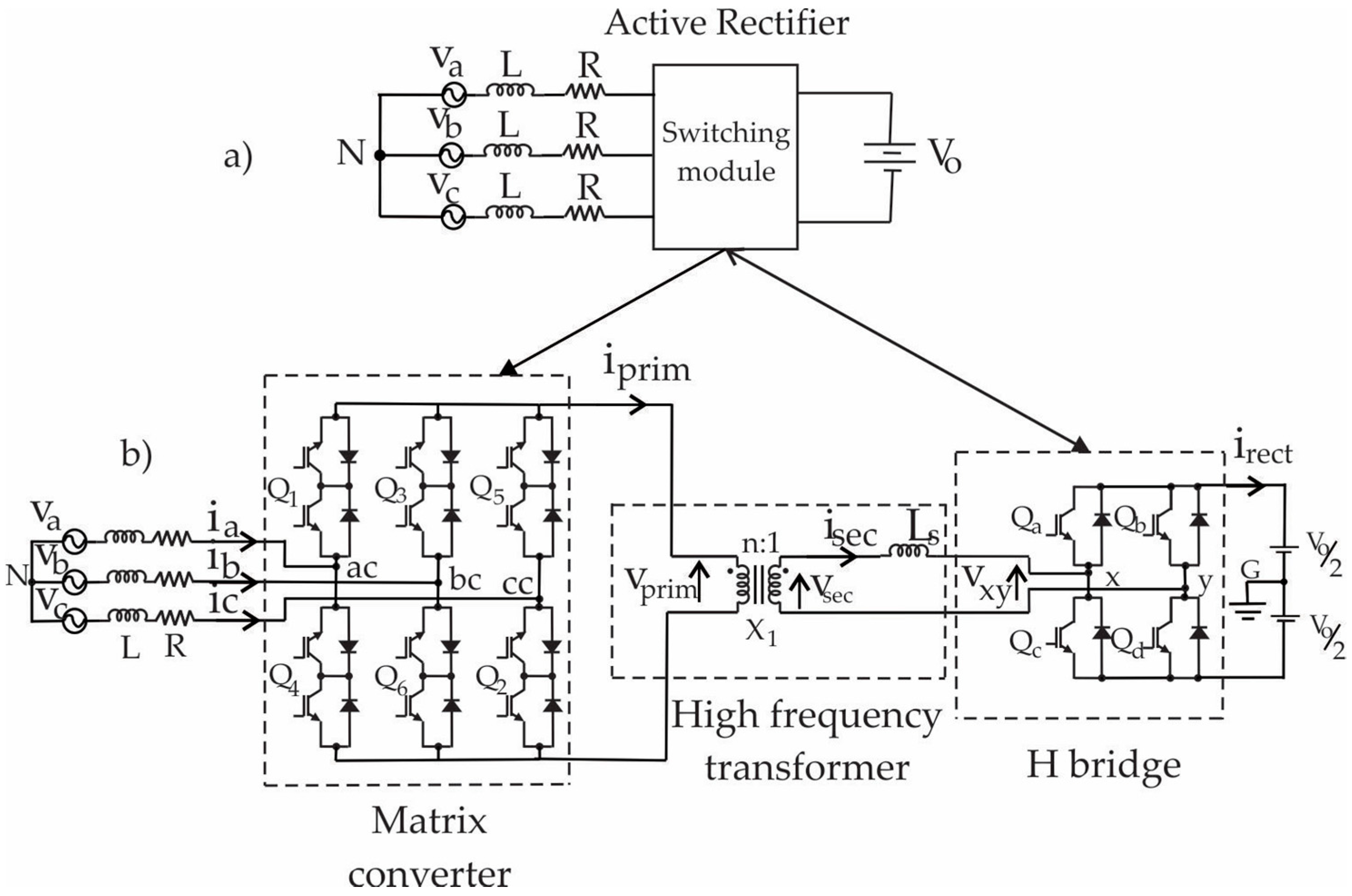
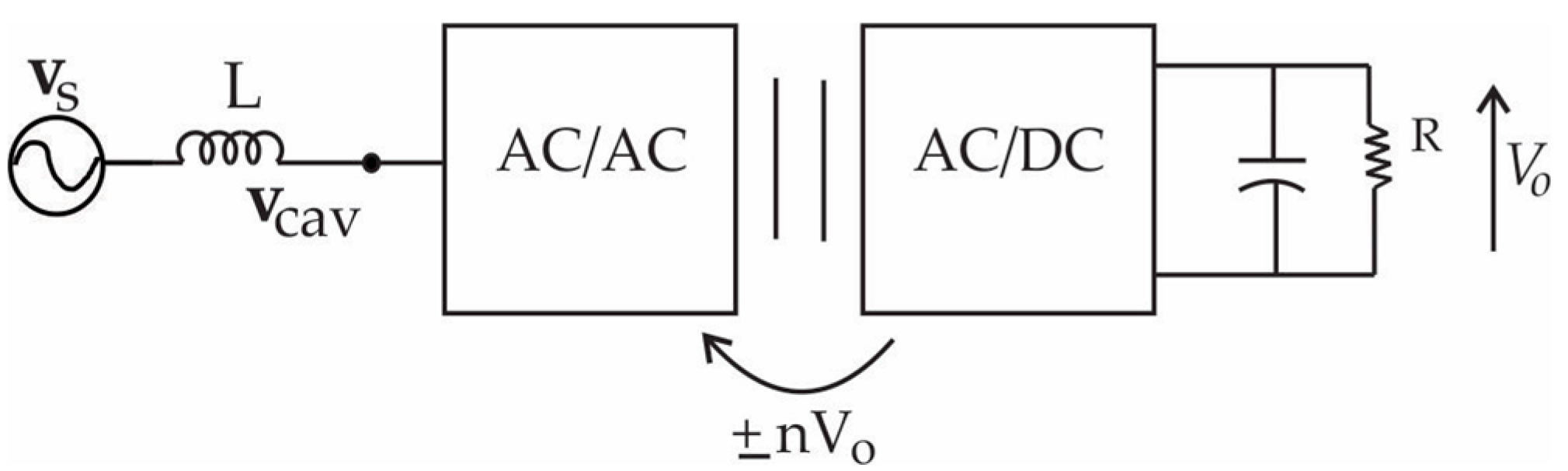
Figure 1.
(a) Conventional active rectifier; (b) Circuit diagram of the proposed modular AC-DC converter.
Figure 1.
(a) Conventional active rectifier; (b) Circuit diagram of the proposed modular AC-DC converter.
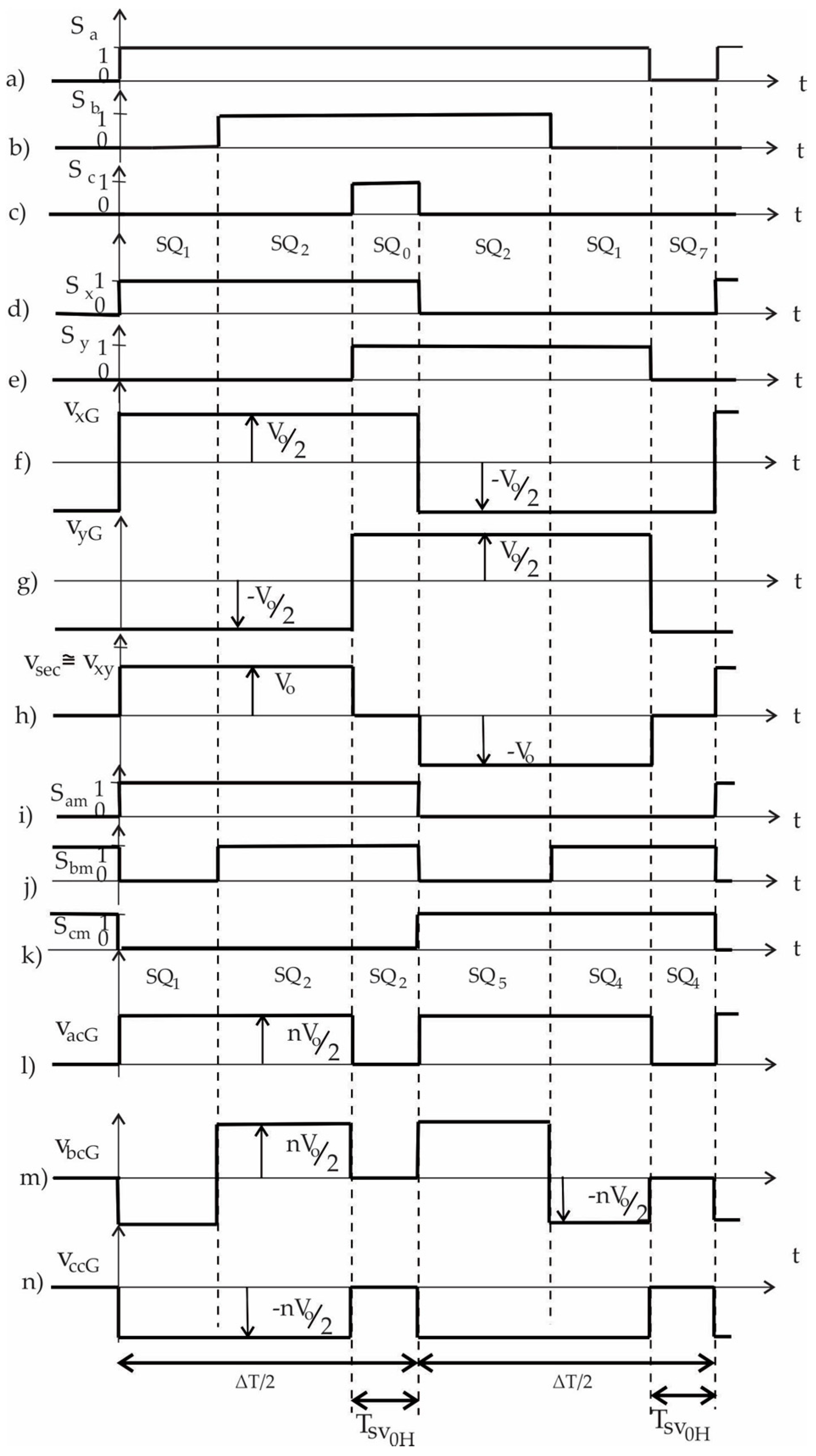
Figure 2.
Derivation of the transistor switching states of the modular active rectifier of
Figure 1b together with their voltage converter waveforms: (
a) switching state
Sa; (
b) switching state
Sb; (
c) switching state
Sc; (
d) switching state
Sx; (
e) switching state
Sy; (
f) voltage
vxG; (
g) voltage
vyG; (
h) voltage
vsec; (
i) switching state
Sam; (
j) switching state
Sbm; (
k) switching state
Scm; (
l) voltage
vacG; (
m) voltage
vbcG; (
n) voltage
vccG.
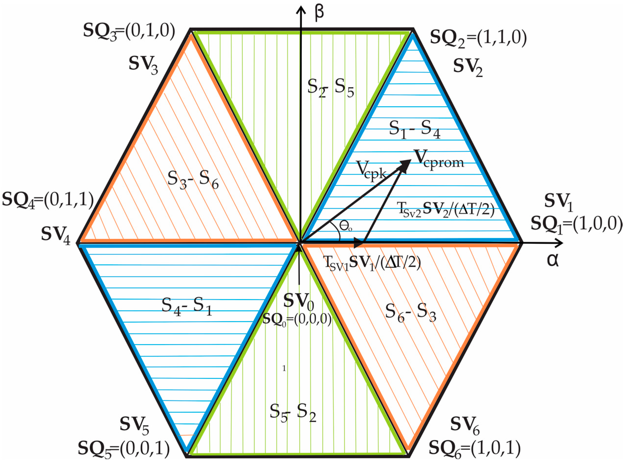
Figure 3.
Space Vector Bi-dimensional plane.
Figure 3.
Space Vector Bi-dimensional plane.
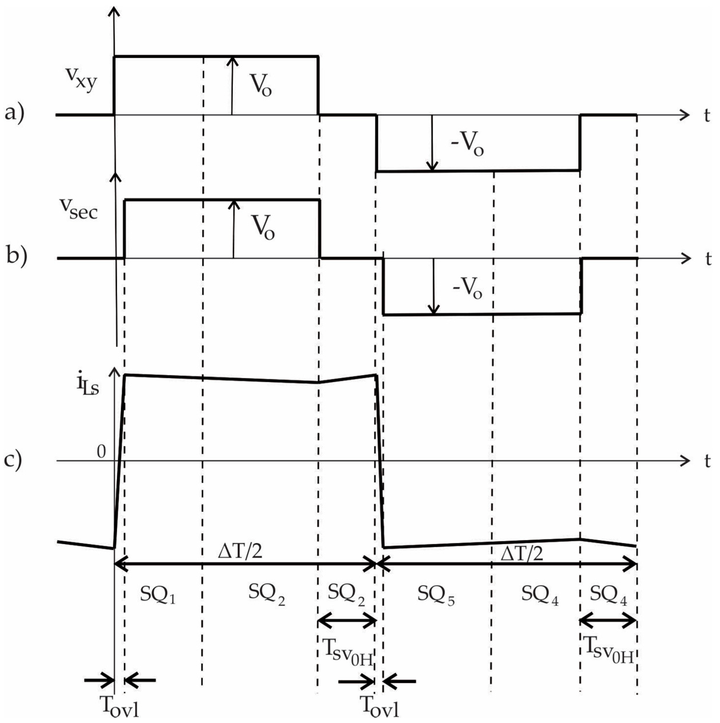
Figure 4.
Ideal wavfeorms: (a) Voltage vxy; (b) voltage vsec; and (c) current through the transformer, iLS.
Figure 4.
Ideal wavfeorms: (a) Voltage vxy; (b) voltage vsec; and (c) current through the transformer, iLS.
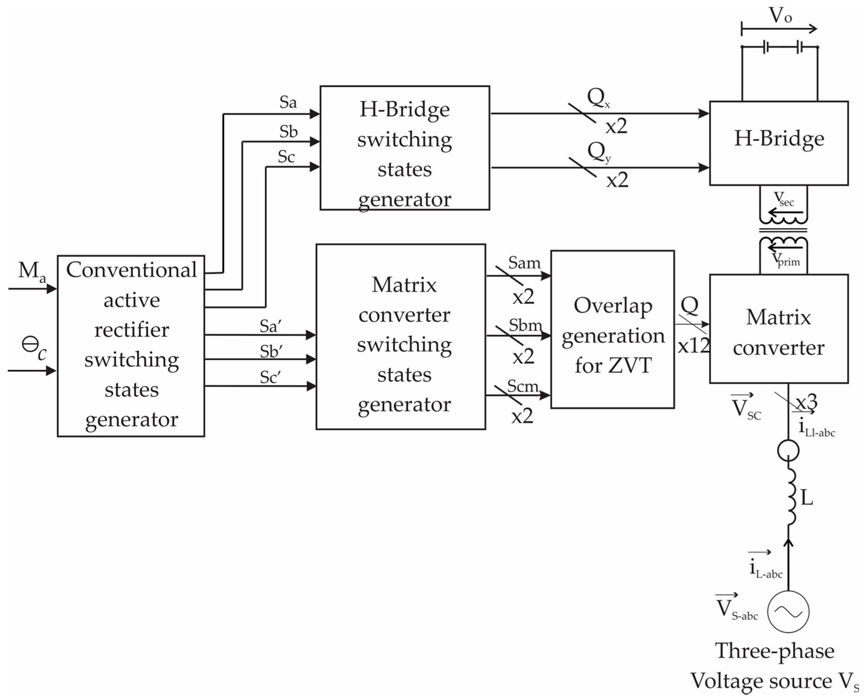
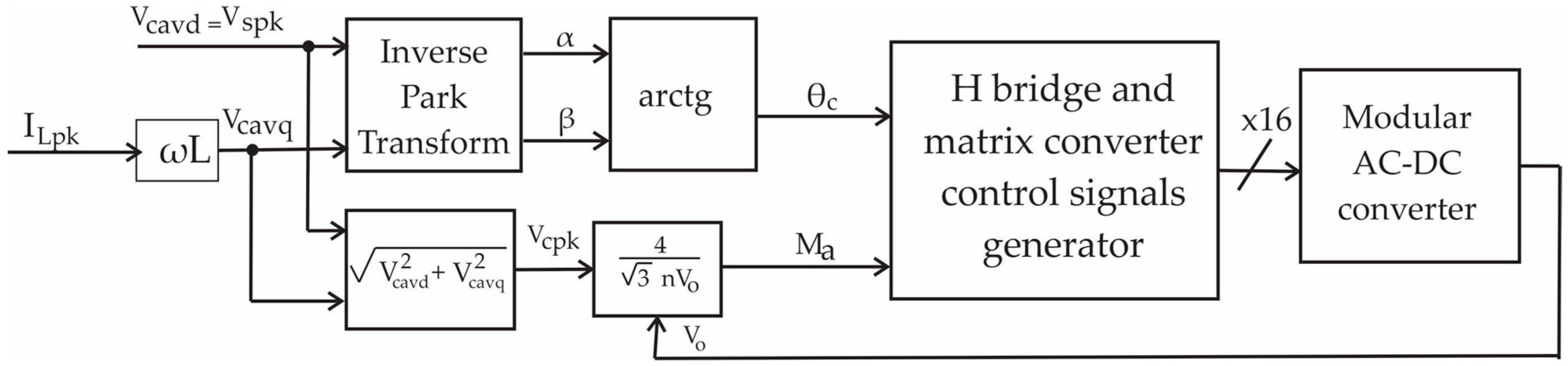
Figure 5.
Block diagram for AC-DC operation of the modular converter of
Figure 1b.
Figure 5.
Block diagram for AC-DC operation of the modular converter of
Figure 1b.
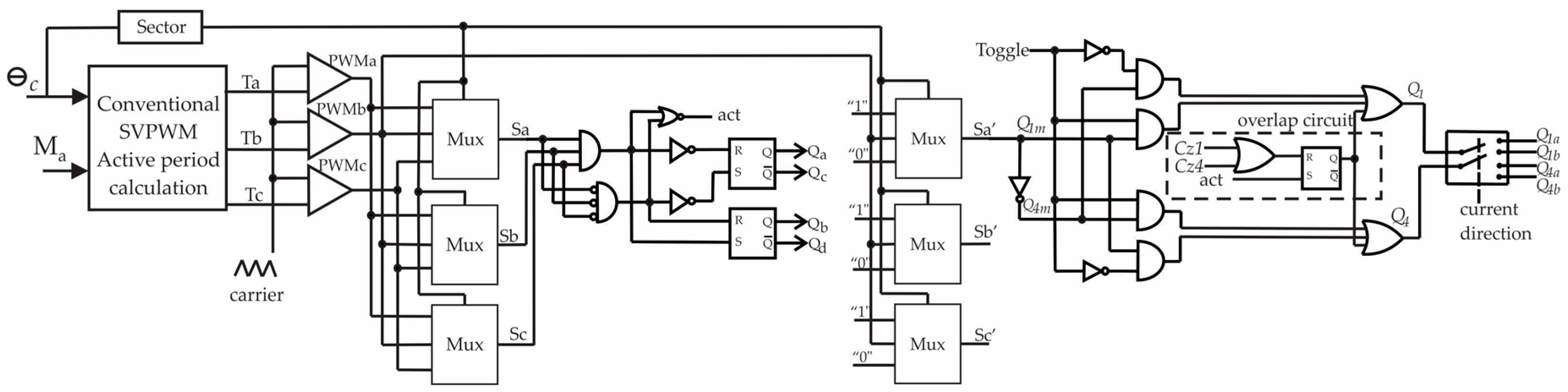
Figure 6.
Block diagram to generate the switching states for the matrix converter and the H bridge.
Figure 6.
Block diagram to generate the switching states for the matrix converter and the H bridge.
Figure 7.
Generation of PWM signals, and conventional active rectifier switching states. (a) High-frequncy triangular carrier signal; (b) digital signal PWMa; (c) digital signal PWMb; (d) digital signal PWMc; (e) switching state Sa; (f) switching state Sb; (g) switching state Sc; (h) digital signal S’a; (i) digital signal S’b; (j) digital signal S’c.
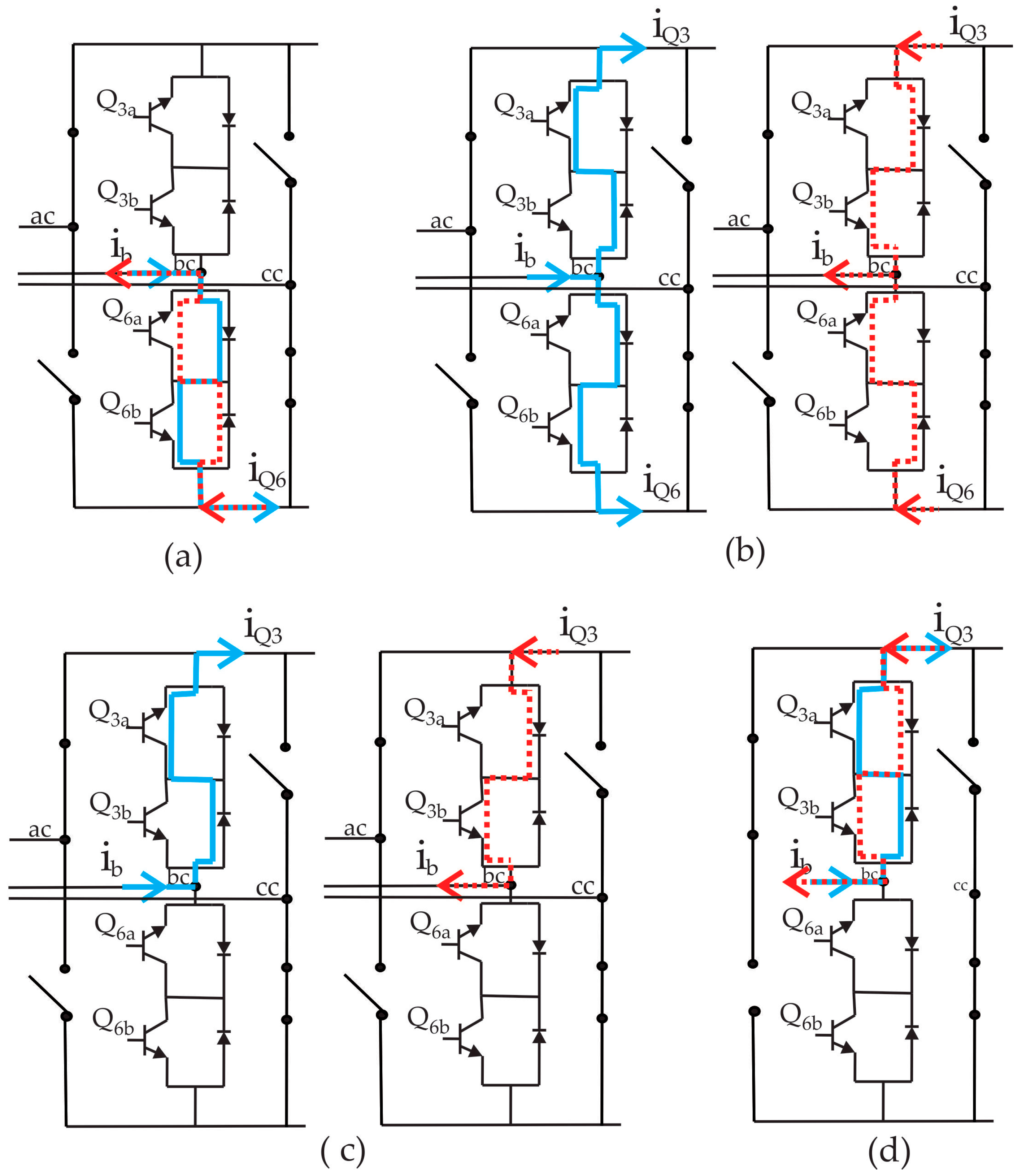
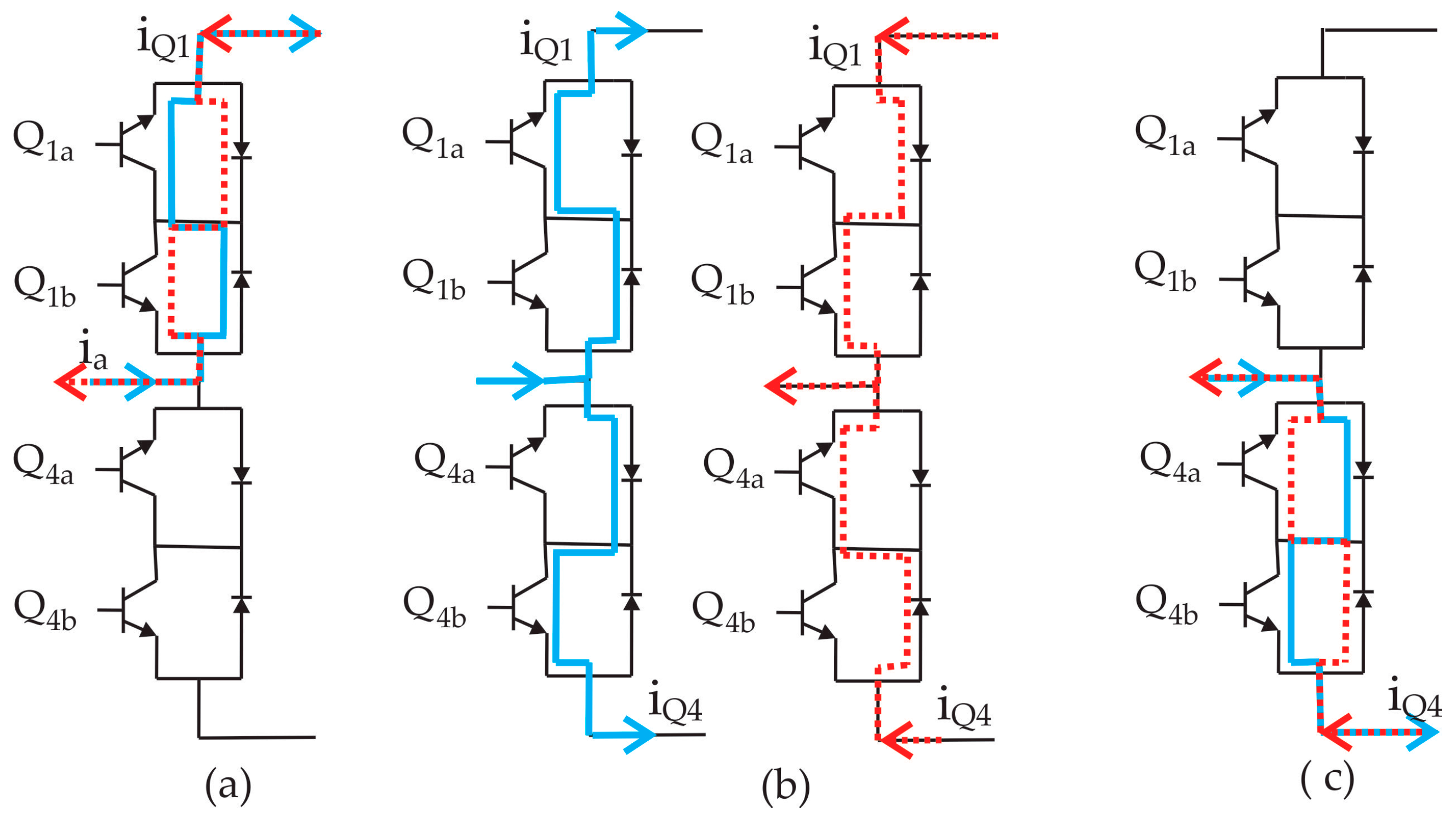
Figure 8.
Switching sequence in the on-to-off transition from neutral-to-active switching state. (a) initial current flow; (b) overlap time; (c) current flow in the opposite direction.
Figure 8.
Switching sequence in the on-to-off transition from neutral-to-active switching state. (a) initial current flow; (b) overlap time; (c) current flow in the opposite direction.
Figure 9.
Switching sequence in the on-to-off transition from active-to-active switching state. (a) initial current flow; (b) overlap time; (c) current flow in the opposite direction; (d) bidirectional switch in on state.
Figure 9.
Switching sequence in the on-to-off transition from active-to-active switching state. (a) initial current flow; (b) overlap time; (c) current flow in the opposite direction; (d) bidirectional switch in on state.
Figure 10.
Generalized diagram for steady-state analysis
Figure 10.
Generalized diagram for steady-state analysis
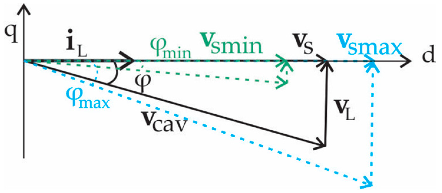
Figure 11.
Phasorial diagram for the AC-DC converter operation.
Figure 11.
Phasorial diagram for the AC-DC converter operation.
Figure 12.
ϕmin and ϕmax obtained for different values of L.
Figure 12.
ϕmin and ϕmax obtained for different values of L.
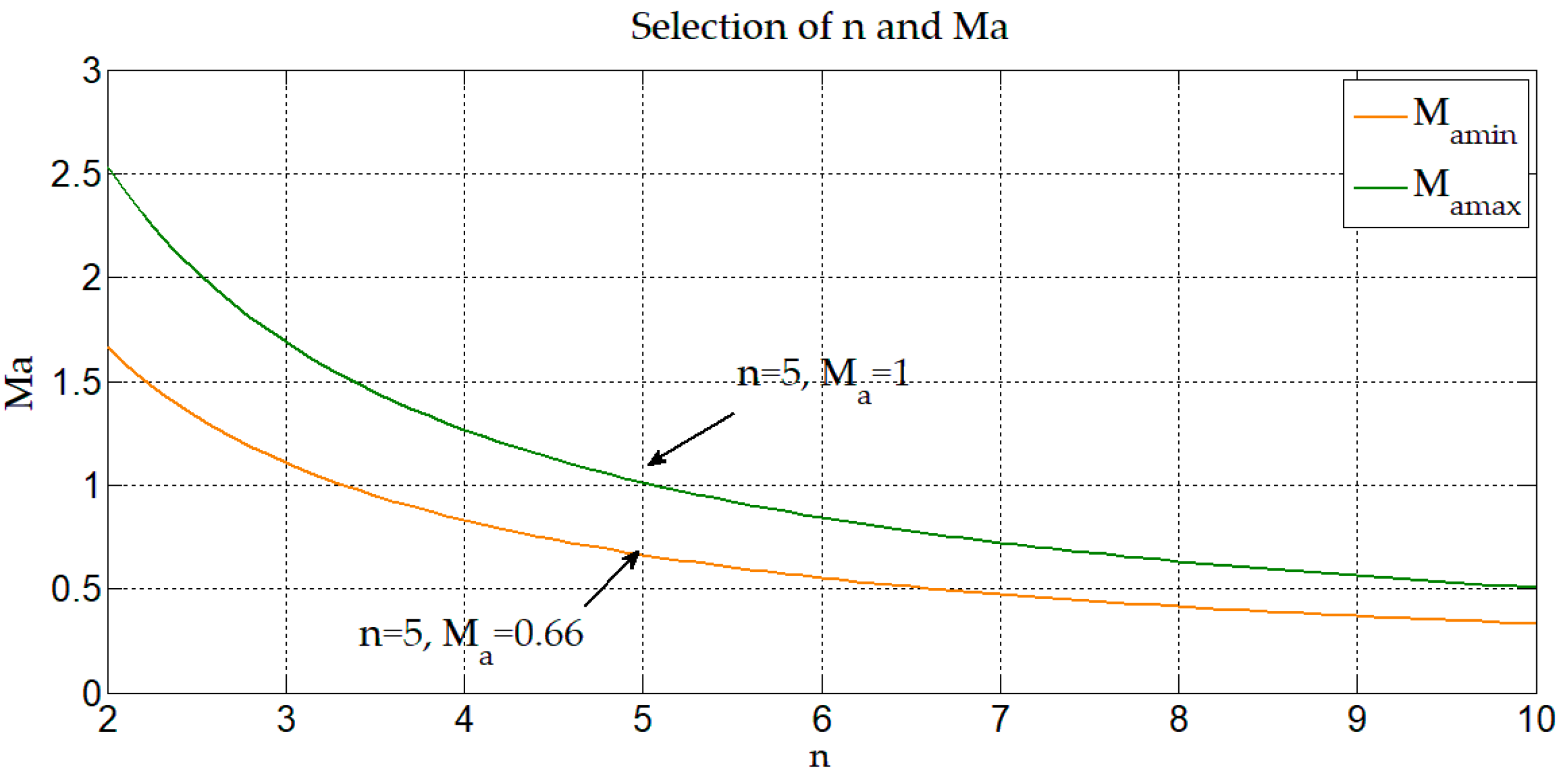
Figure 13.
Mamin and Mamax obtained for different n.
Figure 13.
Mamin and Mamax obtained for different n.
Figure 14.
General scheme used in simulation.
Figure 14.
General scheme used in simulation.
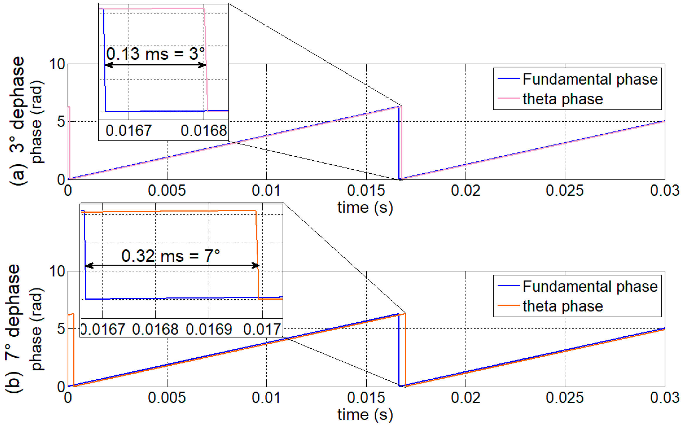
Figure 15.
Variation of φ: (a) φ = 3°; (b) φ = 7°.
Figure 15.
Variation of φ: (a) φ = 3°; (b) φ = 7°.
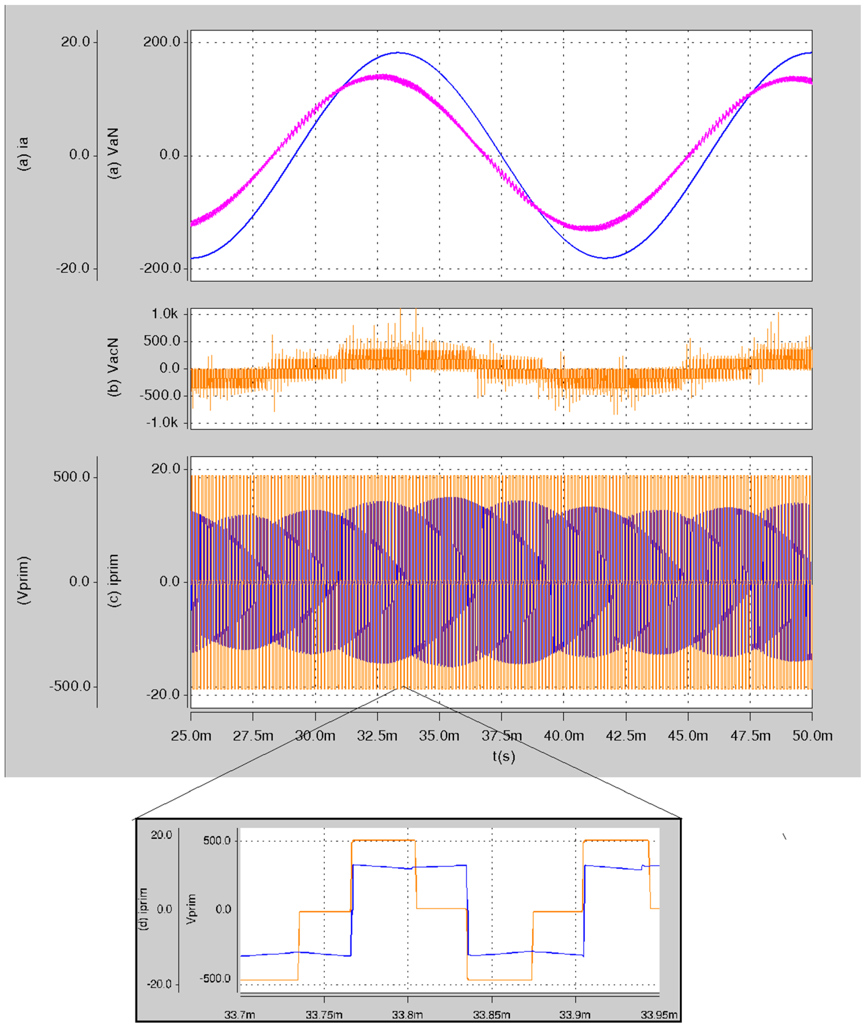
Figure 16.
Simulation results (a) Supply voltage vaN and line current ia; (b) converter voltage in phase a; and (c) High-frequency current and voltage in the primary side of the transformer. Supply: 127 V, 60 Hz, Output: 100 V, 5 kW.
Figure 16.
Simulation results (a) Supply voltage vaN and line current ia; (b) converter voltage in phase a; and (c) High-frequency current and voltage in the primary side of the transformer. Supply: 127 V, 60 Hz, Output: 100 V, 5 kW.
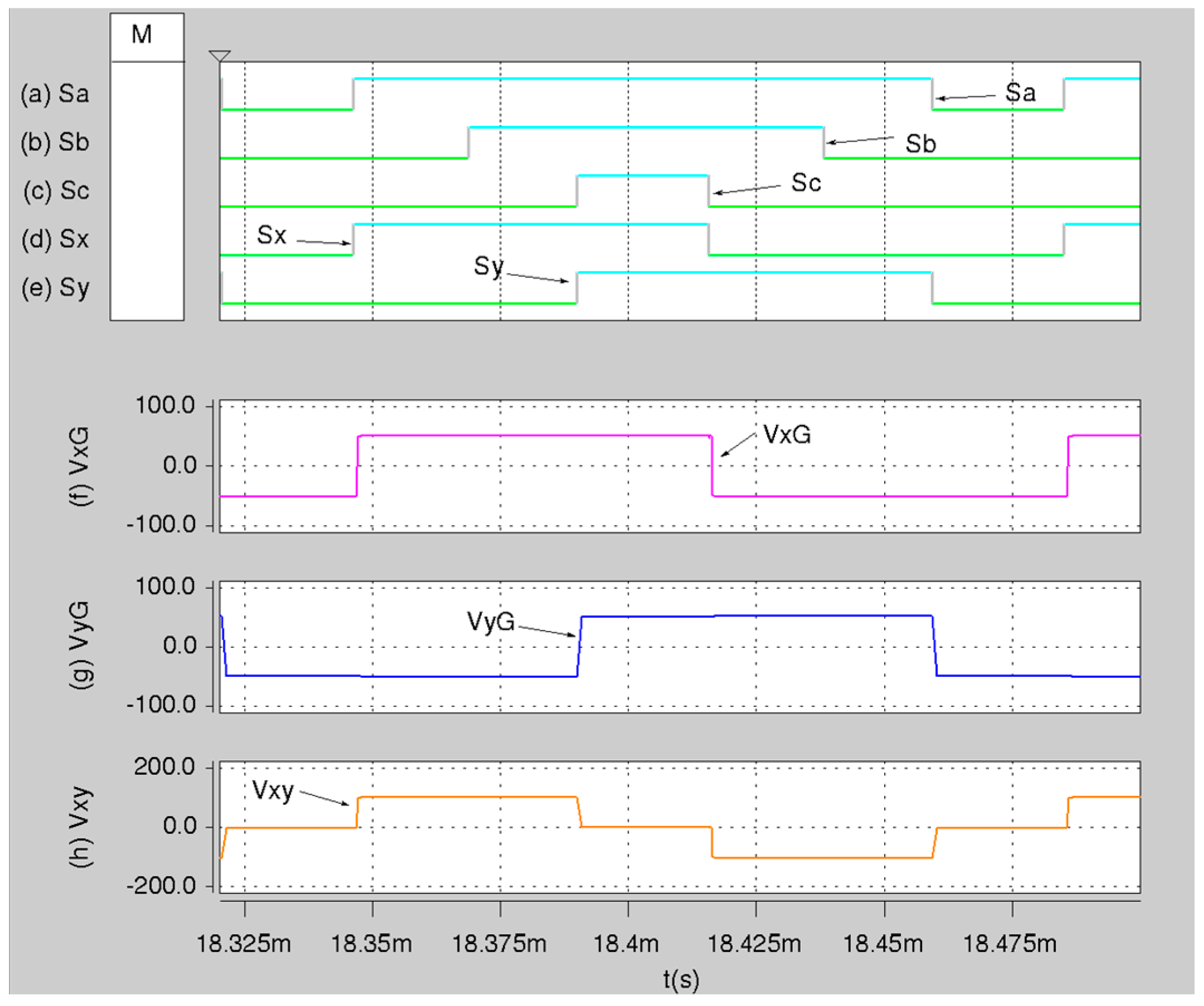
Figure 17.
Simulations results: conventional switching states (a) Sa, (b) Sb and (c) Sc; H-bridge switching states (d) Sx and (e) Sy and voltages (f) vxG (g) vyG and (h) vxy. Supply: 127 V, 60 Hz, Output: 100 V, 5 kW.
Figure 17.
Simulations results: conventional switching states (a) Sa, (b) Sb and (c) Sc; H-bridge switching states (d) Sx and (e) Sy and voltages (f) vxG (g) vyG and (h) vxy. Supply: 127 V, 60 Hz, Output: 100 V, 5 kW.
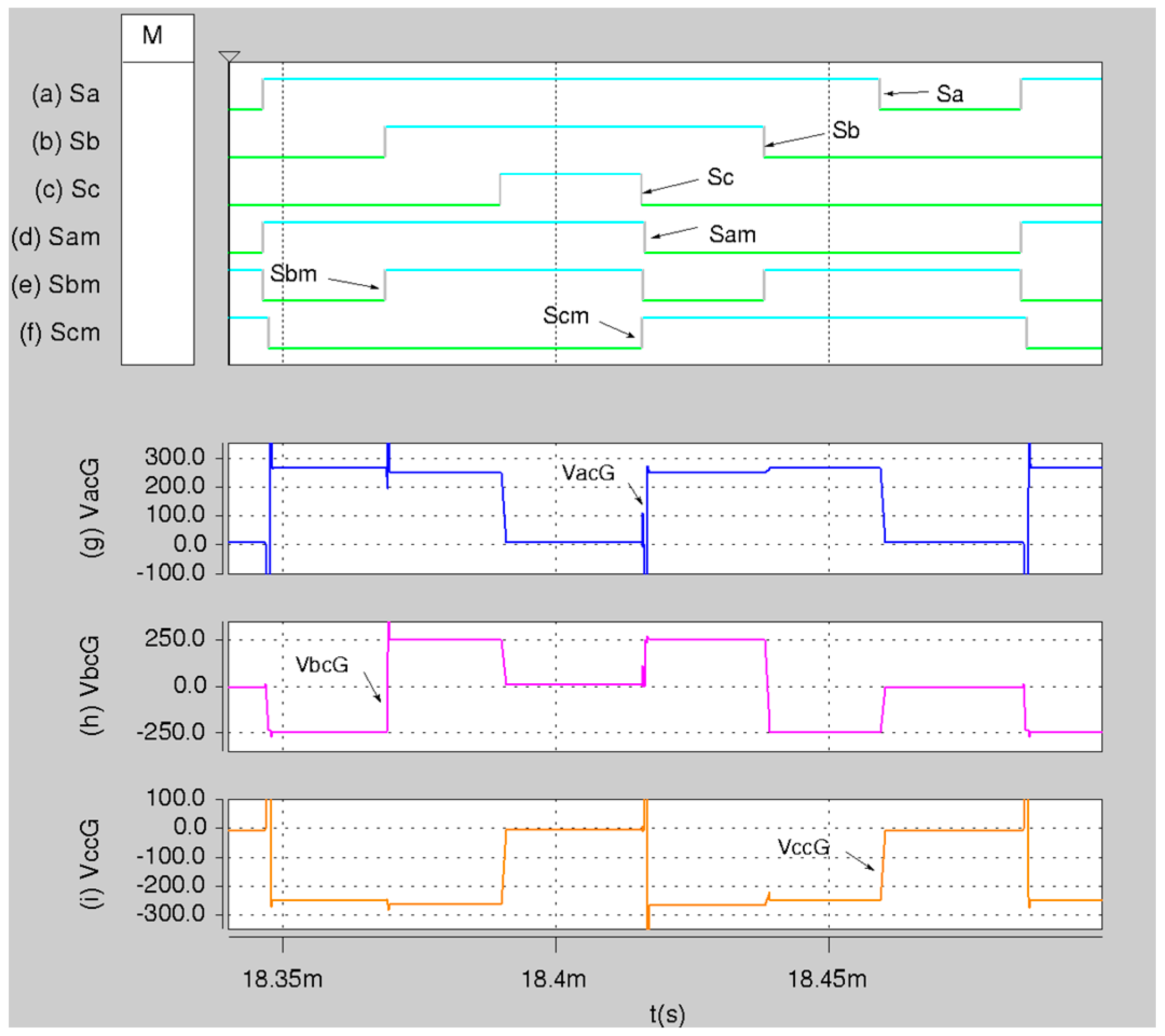
Figure 18.
Simulations results: (a) conventional switching states Sa; (b) Sb; and (c) and Sc; (d) matrix converter switching states Sam; (e) Sbm; and (f) Scm; (g) Voltage vacG; (h) vbcG; and (i) vccG. Supply: 127 V, 60 Hz, Output: 100 V, 5 kW.
Figure 18.
Simulations results: (a) conventional switching states Sa; (b) Sb; and (c) and Sc; (d) matrix converter switching states Sam; (e) Sbm; and (f) Scm; (g) Voltage vacG; (h) vbcG; and (i) vccG. Supply: 127 V, 60 Hz, Output: 100 V, 5 kW.
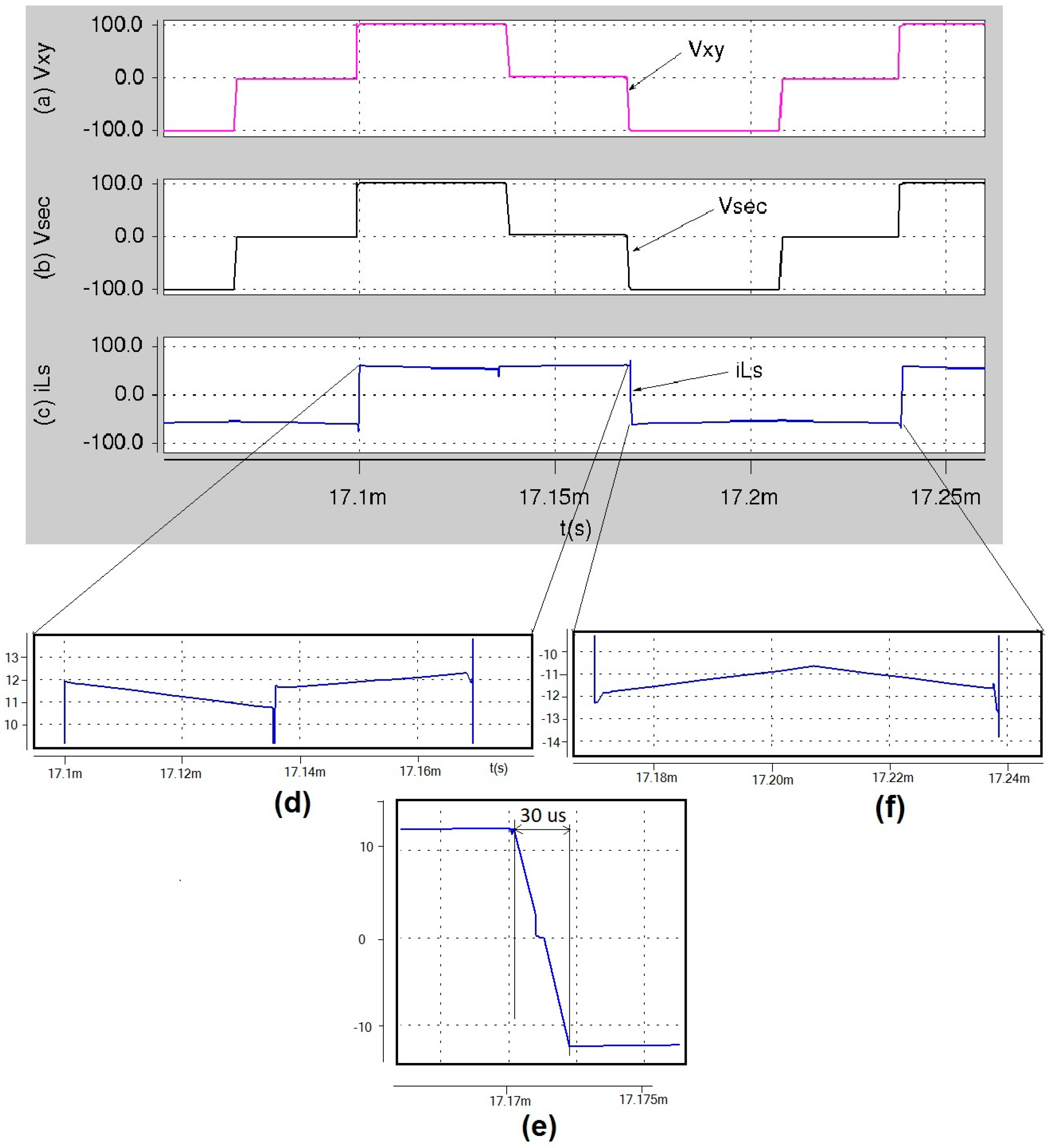
Figure 19.
Simulation results: (a) voltage vxy; (b) vsec; (c) current iLs; (d) Expanded portion of the first semicycle; (e) expanded portion of TovL; and (f) expanded portion of the second semicycle. Supply: 127 V, 60 Hz, Output: 100 V, 5 kW.
Figure 19.
Simulation results: (a) voltage vxy; (b) vsec; (c) current iLs; (d) Expanded portion of the first semicycle; (e) expanded portion of TovL; and (f) expanded portion of the second semicycle. Supply: 127 V, 60 Hz, Output: 100 V, 5 kW.
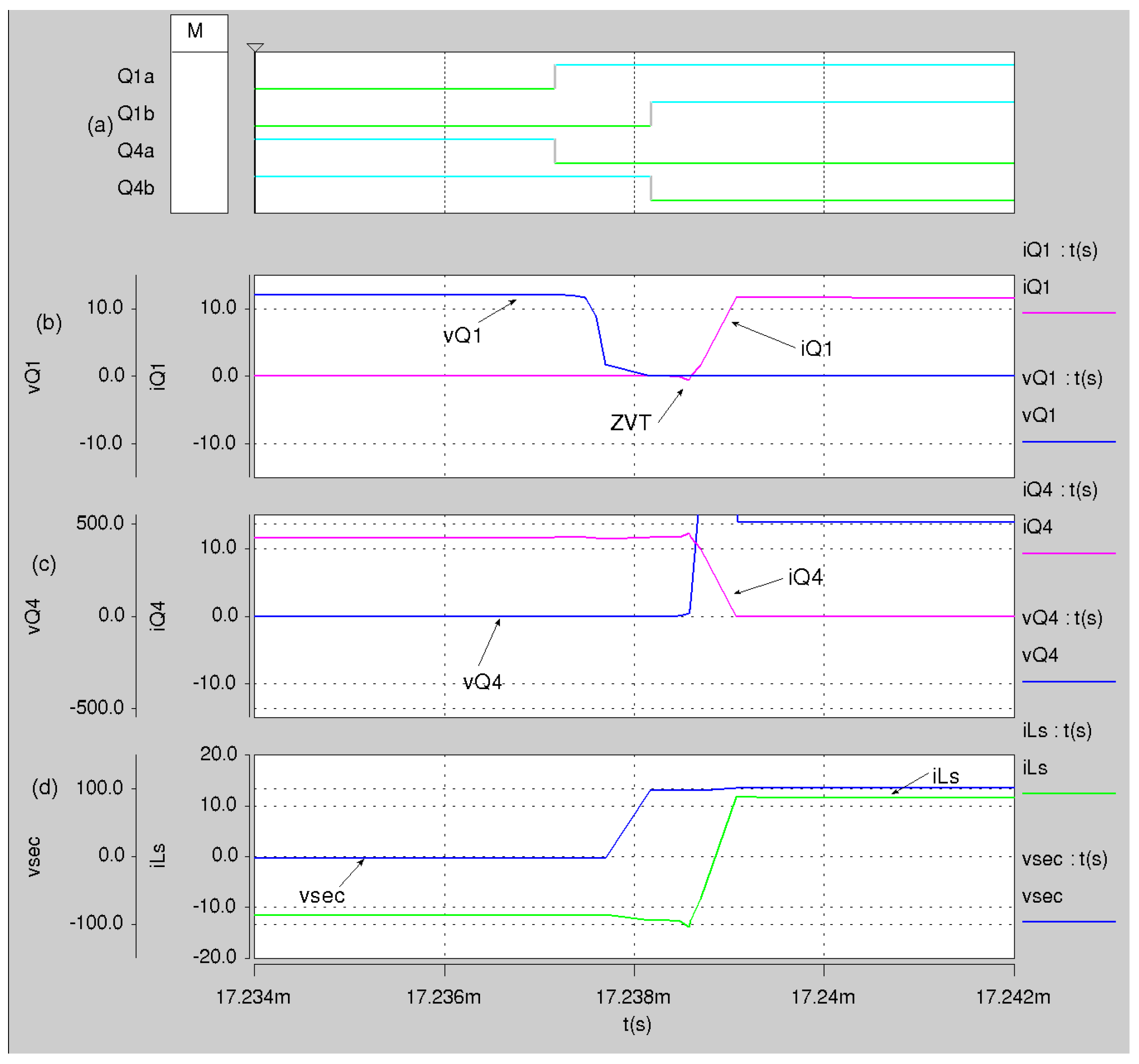
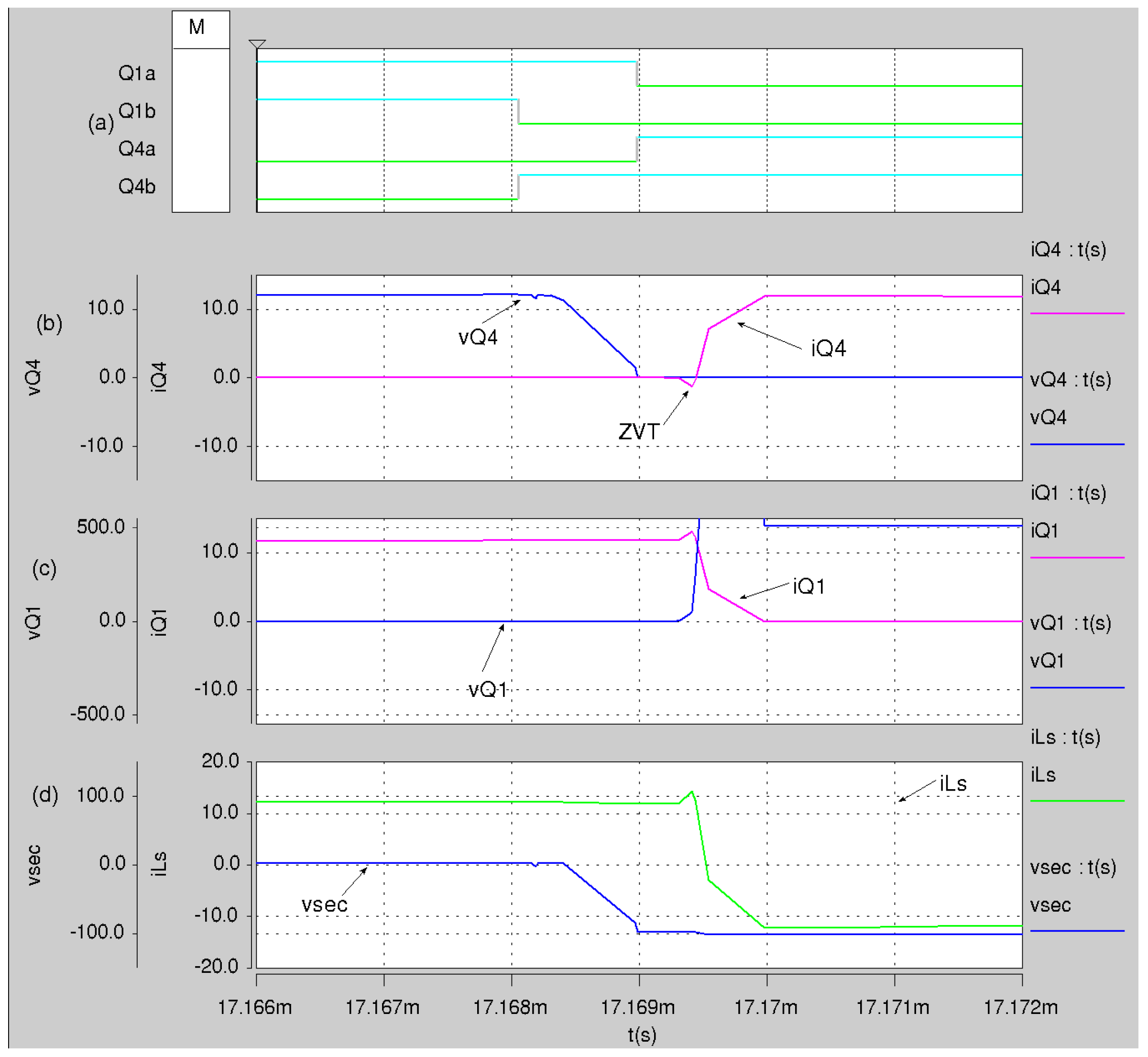
Figure 20.
Simulation results to verify ZVT during the switching transition to turn on Q4, (a) control signals Q1a, Q1b, Q4a, Q4b; (b) iQ4 and vQ4; (c) iQ1 and vQ1; and (d) vsec and iLs. Supply: 127 V, 60 Hz, Output: 100 V, 5 kW.
Figure 20.
Simulation results to verify ZVT during the switching transition to turn on Q4, (a) control signals Q1a, Q1b, Q4a, Q4b; (b) iQ4 and vQ4; (c) iQ1 and vQ1; and (d) vsec and iLs. Supply: 127 V, 60 Hz, Output: 100 V, 5 kW.
Figure 21.
Simulation results to verify ZVT during the switching transition to turn on Q1, (a) control signals Q1a, Q1b, Q4a, Q4b; (b) iQ1 and vQ1; (c) iQ4 and vQ4; and (d) vsec and iLs. Supply: 127 V, 60 Hz, Output: 100 V, 5 kW.
Figure 21.
Simulation results to verify ZVT during the switching transition to turn on Q1, (a) control signals Q1a, Q1b, Q4a, Q4b; (b) iQ1 and vQ1; (c) iQ4 and vQ4; and (d) vsec and iLs. Supply: 127 V, 60 Hz, Output: 100 V, 5 kW.
Figure 22.
Simulations results for (a) iLs; (b) irect. Supply: 127 V, 60 Hz, Output: 100 V, 5 kW.
Figure 22.
Simulations results for (a) iLs; (b) irect. Supply: 127 V, 60 Hz, Output: 100 V, 5 kW.
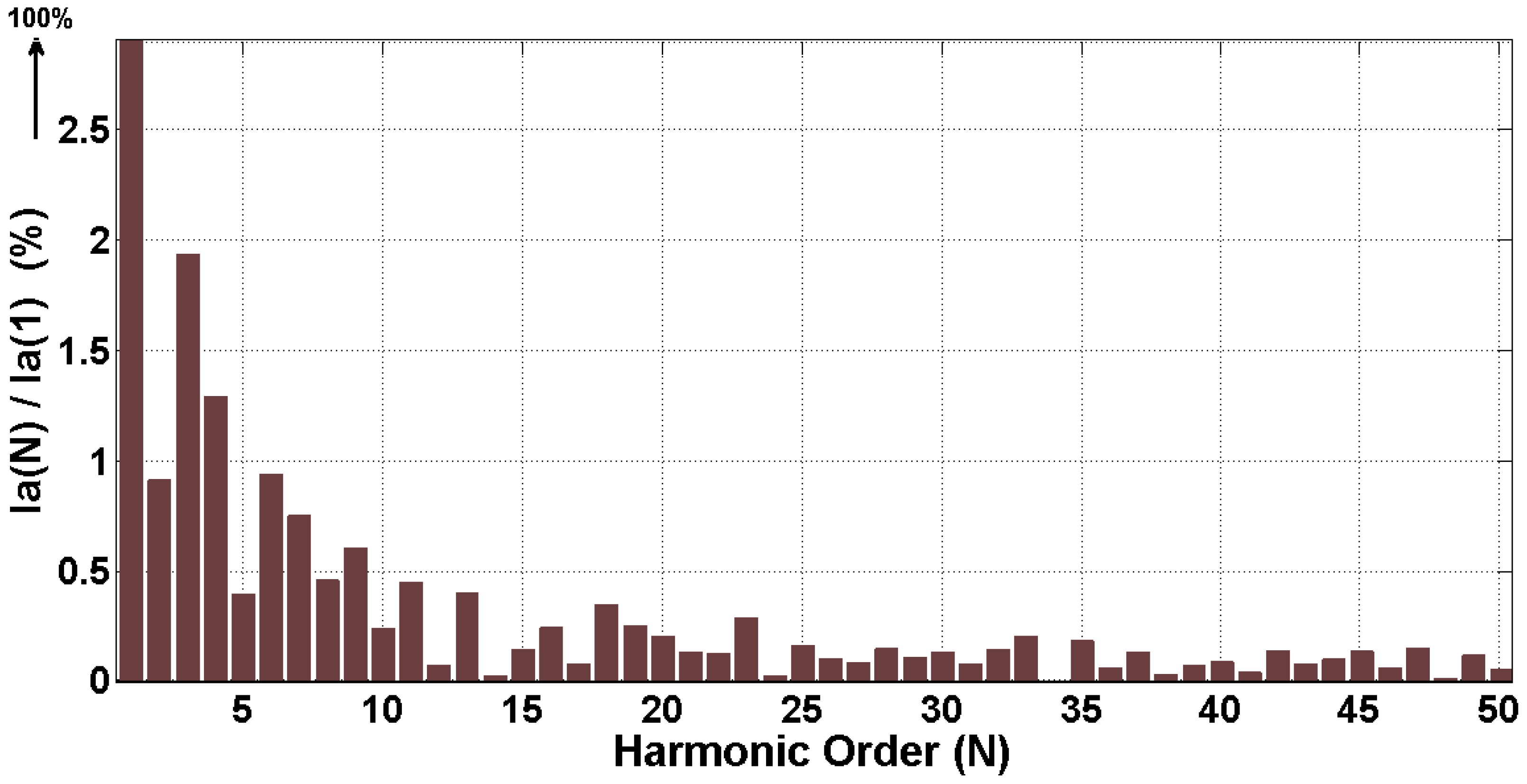
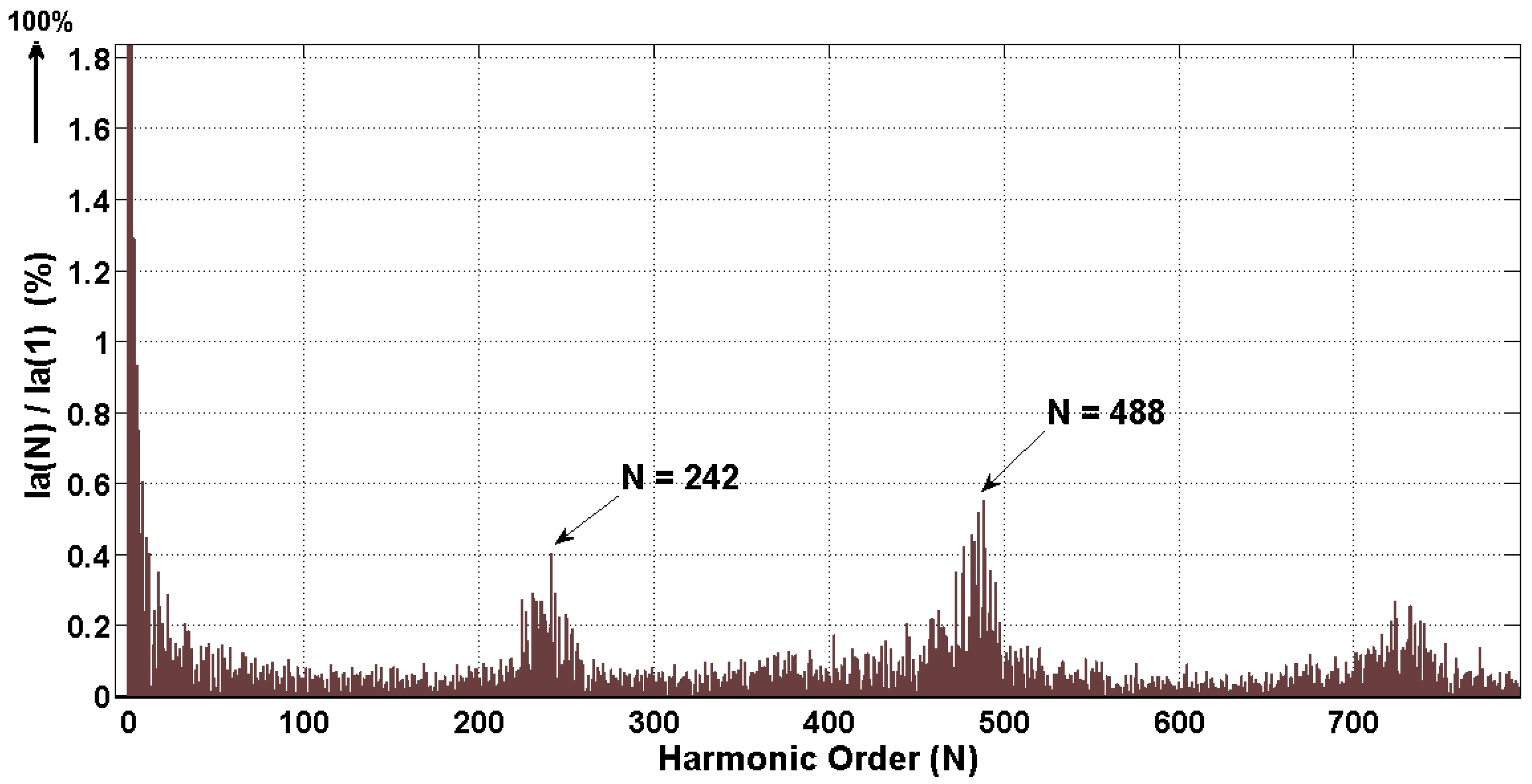
Figure 23.
Harmonic content for line current ia.
Figure 23.
Harmonic content for line current ia.
Figure 24.
Low Harmonic content for line current ia for comparison with Standard EN 61000-3-2.
Figure 24.
Low Harmonic content for line current ia for comparison with Standard EN 61000-3-2.
Table 1.
Switching states vectors of matrix converter.
Table 1.
Switching states vectors of matrix converter.
| Switching State Combination | Sam, Sbm and Scm States |
|---|
| SQ1 | (1, 0, 0) |
| SQ2 | (1, 1, 0) |
| SQ3 | (0, 1, 0) |
| SQ4 | (0, 1, 1) |
| SQ5 | (0, 0, 1) |
| SQ6 | (1, 0, 1) |
Table 2.
Switching states vectors.
Table 2.
Switching states vectors.
| Angle θc | Sector | vprim (+) | vprim (−) |
|---|
| Switching State | Switching State |
|---|
| 1–60° | S1 | SQ1, SQ2 | SQ4, SQ5 |
| 61–120° | S2 | SQ2, SQ3 | SQ5, SQ6 |
| 121–180° | S3 | SQ3, SQ4 | SQ6, SQ1 |
| 181–240° | S4 | SQ4,SQ5 | SQ1, SQ2 |
| 241–300° | S5 | SQ5, SQ6 | SQ2, SQ3 |
| 301–360° | S6 | SQ6, SQ1 | SQ3, SQ4 |
Table 3.
iLS magnitude for each switching state.
Table 3.
iLS magnitude for each switching state.
| Switching State | iprim |
|---|
| SQ1 | iprim = ia − ib − ic |
| SQ2 | iprim = ia + ib − ic |
| SQ3 | iprim = ib – ia − ic |
| SQ4 | iprim = ib + ic – ia |
| SQ5 | iprim = ic − ib – ia |
| SQ6 | iprim = ia − ib + ic |
Table 4.
Simulation Parameters.
Table 4.
Simulation Parameters.
| Parameter | Value |
|---|
| Source voltage va, vb and vc | 180 V peak |
| Source frequency | 60 Hz |
| Switching fequency | 7.2 kHz |
| Input inductor L | 3 mH |
| Index modulation Ma | 0.628 |
| Input resistor R | 0.1 Ω |
| Leakage Inductance Ls | 50 µH |
| Turns ratio n | 5:1 |
| Output voltage Vo | 100 V |
| Output Power Po | 5 kW |
Table 5.
Comparison with three other AC-DC converters.
Table 5.
Comparison with three other AC-DC converters.
| Topology | Proposed AC-DC Modular Converter | Three-Phase PFC Rectifier with DC-DC Converter, [14] | AC-DC Matrix Converter, [14] | Isolated On-Board Vehicle Battery Charger Utilizing SiC Power Devices, [15] | Inductively Coupled Multi-Phase Resonant Wireless Converter, [16] |
|---|
| Factor | |
|---|
| Level | 3 | 2 | 2–3 | 1–2 | 1 |
| Supply voltage phases | 3 | 3 | 3 | 1 | 1 |
| Switching Devices | 16 (4 on board) | 12 | 12 | 6 | 6 |
| THD | 4.40% | <5% | <1% | 4.20% | <5% |
| Switching losses | Virtual 0 W (ZVT) | 241.1 W | 165.2 W | 0 W (using ZVT) | 0 W (using ZVT) |
| Switching Frequency | 7.2 kHz | 10 kHz | 10 kHz | 250 kHz | 83–88 kHz |
| Capability to reverse power flow | Yes | No | Yes | No | No |
| Possibility to split the converter | Yes | No | No | No | Yes |
| Output Power | 5–20 kW | 22.6 kW | 20.4 kW | 6.1 kW | 1 kW |
| Efficiency | 95.8% (estimated) | 97.72% | 96.80% | 94% | 93.34% |
| Total Volume On-Board Converter | 1700 cm3 (Estimated) | 8430 cm3 | 6668.5 cm3 | 1742 cm3 | 5250 cm3 (Estimated) |
| Power Density | 10 kW/dm3 (Estimated) | 3.8 kW/dm3 | 4.3 kW/dm3 | 5 kW/dm3 | 192 W/dm3 (Estimated) |
| Advantages over others | Reduces the size of the converter located on-boar the vehicle. The SVPWM together with ZVT generate high-quality sinusoidal currents with null switching losses | Eliminates harmonics, improves the power factor, great simplicity, stable and reliable operation | The volume of the reactive components is reduced. Passive components are not needed in intermediate steps | The switching frequency is increased, the size and weight is reduced | Full-range regulation from zero to full power without switching losses |
| Major Drawbacks | The efficiency can be reduced by using the transformer | Need to be followed by a step-down DC-DC converter. Passive components are required in intermediate steps | The converter is on-board the vehicle. When the switching devices reach the temperature of 145°, the maximum output power decreases | The conversion is made by three steps with intermediate passive components. Not suitable for high power applications | Not suitable for high power applications. More than transformers are used, increasing the losses |


