
Maximum Boost Control Method for Single-Phase Quasi-Switched-Boost and Quasi-Z-Source Inverters


Department of Electrical Engineering, University of Chosun, Gwangju 61452, Korea
*
Author to whom correspondence should be addressed.
Energies 2017, 10(4), 553; https://doi.org/10.3390/en10040553
Submission received: 3 March 2017
/
Revised: 10 April 2017
/
Accepted: 14 April 2017
/
Published: 18 April 2017
(This article belongs to the Section I: Energy Fundamentals and Conversion)
Abstract
:The maximum boost control method for a single-phase switched-boost inverter (SBI) and single-phase Z-source inverter (ZSI) is proposed in this paper. In the proposed method, the low frequency voltage is added to the constant voltage for generating the variable shoot-through time intervals. For improving the AC output quality of the inverter, an active power switch is used to replace one of the diodes in the single-phase SBI. The operating principles and circuit analysis using the proposed maximum boost control method for single-phase inverters are presented. Laboratory prototypes are built to verify the operation of the proposed pulse-width modulation (PWM) control method for both single-phase quasi-ZSI and single-phase quasi-SBI.
1. Introduction
Many control schemes including carrier-based pulse-width modulation (CB-PWM) and space vector pulse-width modulation (SV-PWM) have been proposed for controlling the shoot-through time interval in three phase Z-source inverters (ZSIs) [1,2,3,4,5,6,7]. Four basic CB-PWM control techniques, namely simple boost control [1], maximum boost control [2], maximum constant boost control [3], and modified SV-PWM methods [6,7] for three-phase ZSIs were compared in [8]. For single-phase ZSIs, most PWM controls use the simple boost control method [9,10,11,12,13,14,15,16]. In the simple boost control method, a constant voltage is compared to a high frequency triangle waveform to generate a fixed shoot-through control signal. As a result, the modulation index in the simple boost control method is limited to (1-D), where D is the shoot-through duty cycle. On the other hand, the modulation index in this modulation technique is decreased whereas the shoot-through range is increased. In order to reduce the power loss, a hybrid PWM single-phase quasi-Z-source grid-tie photovoltaic power system is proposed in [17]. In the hybrid PWM strategy, a combination between PWM and pulse-amplitude modulation (PAM) is addressed for the single-phase quasi-Z source inverter (qZSI). When the AC output voltage is lower than the DC source voltage, the PWM strategy is used. When the AC output voltage is higher than the DC source voltage, the PAM strategy is applied.
Recently, some PWM strategies to reduce the ripples in the capacitor voltage and inductor current of ZSIs have been addressed in [11,12,13,18,19]. In [13], a low frequency (2ω) ripple is added to the constant shoot-through control waveform to suppress the double-frequency ripple in the capacitor in the single-phase ZSI topology. In order to minimize the inductor current ripple in the three-phase ZSI topology, a PWM scheme in which the shoot-through time intervals of the three phase legs are calculated and rearranged according to the active state and zero state time intervals has been proposed in [19]. Instead of using PWM control strategies to reduce the low-frequency ripple, an active filter integrated single-phase qZSI topology has been proposed in [14] to transfer the low-frequency ripple directly from the AC load to the active filter AC capacitor.
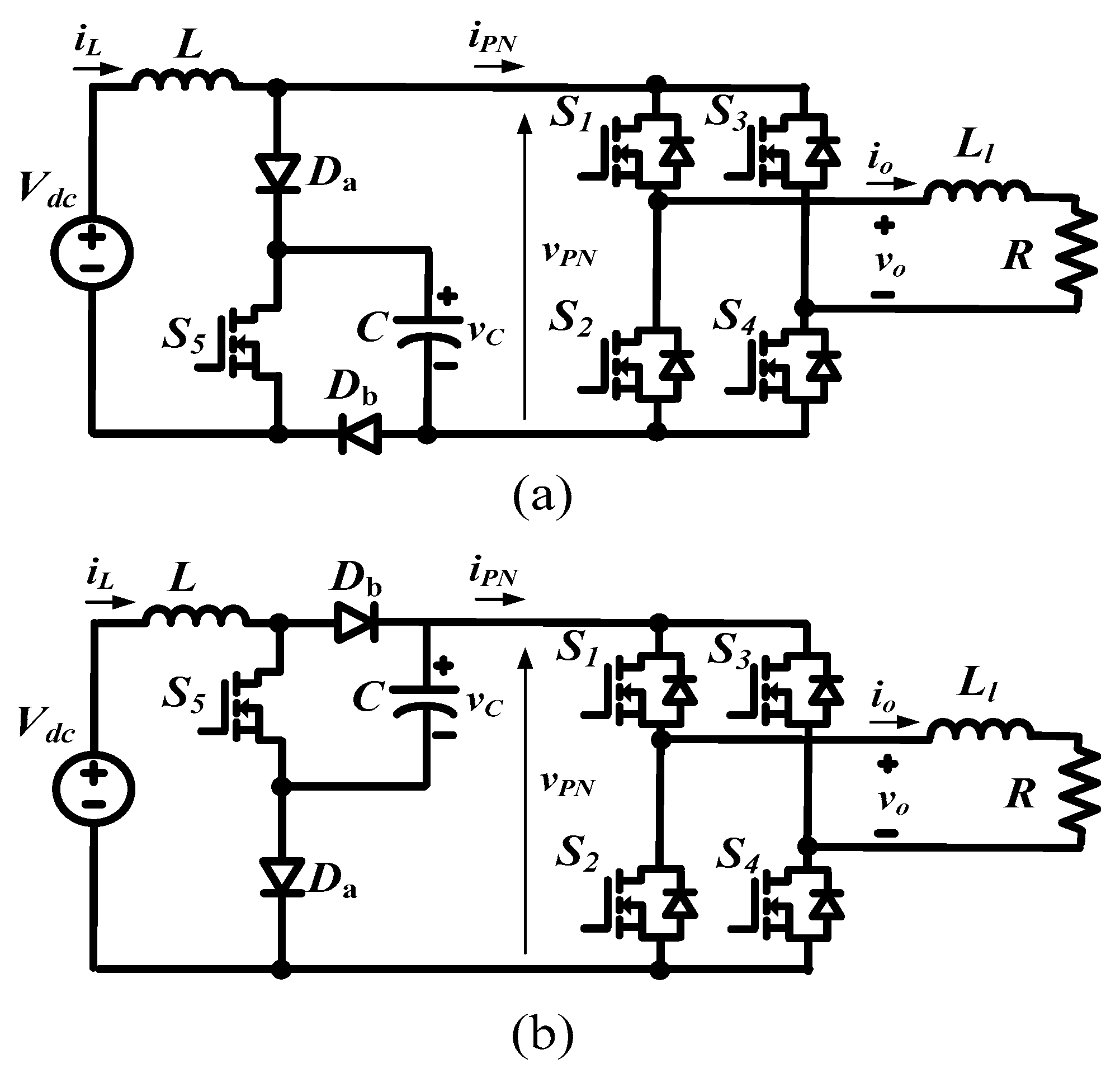
Figure 1 shows the single-phase qZSI [11,12,13]. Compared to ZSI, qZSI improves the input current and reduces the capacitor voltage rating. Like ZSI/qZSIs, switched-boost inverters (SBIs) [20,21,22,23,24,25,26] also use the shoot-through time interval to achieve single-stage power conversion with buck-boost characteristics and improve reliability. In comparison with ZSIs, SBIs use one more active switch and fewer passive components [20]. Thus the size, weight, and cost of power inverters can be decreased. An SBI for standalone DC nanogrid applications is presented in [21]. In the basic SBI topology [22], the input current is discontinuous and its boost factor is lower than that of ZSIs. Quasi-switched boost inverters (qSBIs) [23,24] overcome the shortcomings of conventional SBIs by improving the profile of the input current and reducing the voltage stress of the capacitor. In [25], the concept of a switched inductor is applied to the SBI topologies to improve the boost factor. Compared to conventional SBIs, switched-inductor boost inverters [25] add only three diodes and one inductor to produce a high step-up DC-link voltage. The active switched-capacitor/switched-inductor qZSIs presented in [26] are also based on switched-inductor boost inverter topologies [25].
Because a shoot-through interval is also applied to SBIs to boost the DC-link voltage, the PWM control strategy used for SBIs is the same as that used for ZSIs. In the single-phase SBI [20,21,22,23,24,25], a simple boost PWM control method is usually used. When a high modulation index is used to improve the output voltage quality, the shoot-through duty cycle must be reduced and an undesirable mode appears in the non-shoot-through state of the single-phase SBI. As a result, the DC-link voltage of the single-phase SBI is unstable during the non-shoot-through state.
In this paper, one of the diodes in the single-phase SBI is replaced by an active power switch to improve the AC output quality when a small shoot-through duty cycle is used. Moreover, the maximum boost control method for single-phase SBIs and ZSIs is proposed to increase the boost factor. The operating principles and analysis of single-phase SBIs are presented. Laboratory prototypes are built to verify the operation of the proposed PWM method for both single-phase qZSIs and single-phase qSBIs.
2. Single-Phase qSBI under Small Shoot-Through Duty Cycle Operating Conditions
Figure 2 shows two variants of the single-phase qSBI topology: types 1 and 2. The circuit consists of one inductor (L), one capacitor (C), six diodes, five active switches, and a passive load (R and Ll). The two topologies utilize the same components as those utilized by the basic SBI topologies presented in [23]. Under lossless conditions, the fundamental voltage and current of AC output for a single-phase qSBI are and , respectively, where ω is the angular frequency, Φ is the impedance angle, and Vm and Im are the peak values of the AC output voltage and current, respectively. Figure 3 shows the operating states of the type 2 qSBI using small shoot-through duty cycle. In the shoot-through state, as shown in Figure 3a, the inverter side is shorted by both the upper and lower switching devices of any phase leg. The time interval in this state is D·T, where D is the shoot-through duty cycle and T is the switching period. During the shoot-through state, the switch S5 is turned on, while the diodes Da and Db are turned off. The capacitor C is discharged while the inductor L stores energy. The DC-link voltage is zero. Therefore, the inverter does not generate the power to load in this state.
In the non-shoot-through state, as shown in Figure 3b, the inverter has two active states and two zero states of the inverter main circuit in single-phase topology. The time interval in this state is (1 − D)·T. During the non-shoot-through state, Da and Db are turned on, while S5 is turned off. The capacitor C is charged from Vdc, while the inductor L transfers energy from the DC voltage source to the main circuit. The DC-link voltage is the capacitor voltage.
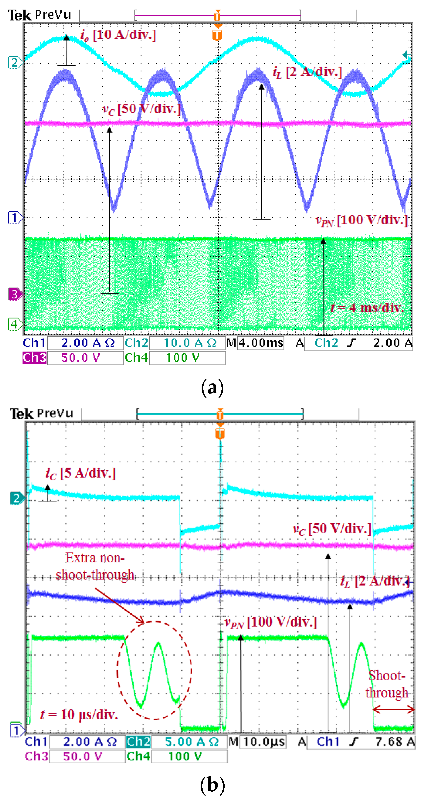
When a small shoot-through duty cycle is used to increase the modulation index, the inverter has an extra state, as shown in Figure 3c. In this state, the inductor current is equal to the DC-link current, iDC. As a result, the capacitor current becomes zero, and Da is turned off. The DC-link voltage in this case is:
The inverter produces the main power to load in the non-shoot-through state. Thus, the output power is:
The DC-link current is calculated by:
where M is the modulation index of the H-bridge inverter.
Substituting Equation (3) into Equation (1), the DC-link voltage in the extra non-shoot-through state is calculated by:
Therefore the DC-link voltage in the non-shoot-through state equals either Vc or . As a result, the inverter produces an unstable DC-link voltage, and the total harmonic distortion (THD) of the output current is increased.
Figure 4 shows the experimental waveforms of the type 2 single-phase qSBI when Vdc = 120 V, D = 0.2, and M = 0.8. The experimental parameters are L = 6 mH, C = 2000 μF, Lf = 5 mH, and R = 20 Ω. As shown in Figure 4b, the DC-link voltage is unstable during the non-shoot-through state when the shoot-through duty cycle is small. The measured THD of the output current is 5.5%.
In order to eliminate the undesired operation state as shown in Figure 3c, one simple method is addressed in which Da is replaced by an active switch, S6. The improved configuration of qSBI is shown in Figure 5. S5 and S6 have a common drain in Figure 5a, whereas they have a common source in Figure 5b. The gate signal of S6 is complementary to that of S5. By using this topology, the inverter produces a stable voltage in the DC link during the non-shoot-through state to improve the AC output quality without the aforementioned limitation.
3. Proposed Maximum Boost Control Method for Single-Phase Switched Boost and Z-Source Inverters
In single-phase qZSIs [8,9,10,11,12,13,14,15,16] and single-phase qSBIs [20,21,22,23,24], a simple boost PWM control method is usually used. In this method, a constant voltage is compared to a triangle waveform to generate a control signal for the shoot-through state. As a result, the maximum duty ratio of the shoot-through state is limited by (1–M) to ensure that the shoot-through interval is only inserted into the traditional zero states. When a large shoot-through duty cycle is used, the modulation index must be reduced. Using a low modulation index reduces the overall DC-to-AC inversion gain and increases the THD value [4].
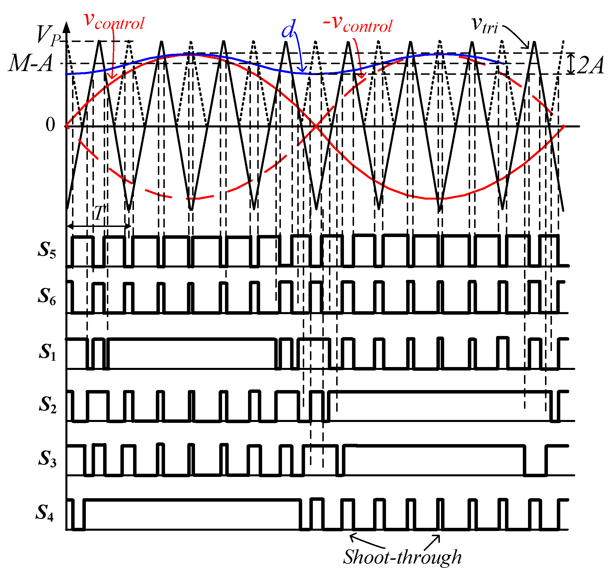
Figure 6 shows the proposed maximum boost PWM control method for single-phase qSBIs to improve the modulation index. Two sinusoidal control waveforms, vcontrol and −vcontrol, with amplitude value M are compared to a high frequency triangle waveform, vtri, to generate control signals for the switches S1–S4. A double line frequency sine waveform voltage d is compared to another triangle waveform (indicated by the dashed line) with double the frequency and half the amplitude of vtri to generate a control signal for S5. The S5 control signal is then applied as the input control signals to the switches S1 to S4 through OR logic gates to generate the shoot-through states in the inverter bridge.
In the maximum boost PWM control method, the peak value of d is the same as that of the control waveforms. If the modulation index is denoted by M, the function for d is given as:
where A is half the peak-to-peak value of d as shown in Figure 6.
The average shoot-through duty cycle is calculated by:
For the same modulation index, the shoot-through duty cycle in the maximum PWM control method produces a greater increment in A compared to that produced by the simple PWM control method. On the other hand, for the same shoot-through duty cycle, the modulation index in the proposed method increases to:
4. Circuit Analysis
For the AC component circuit analysis of the improved SBI and qZSI, the following assumptions hold true:
- the inverter power losses are ignored
- the DC voltage source is constant
- the inverter is operating in a continuous conduction mode, and
- all the variables are expressed by a DC component and a small signal perturbation as follows:
4.1. Circuit Analysis for Single-Phase Improved SBI
In order to improve the modulation index, a small shoot-through duty cycle is used. Thus, the improved single-phase qSBI as shown in Figure 5 is used to eliminate the undesired operation state of Figure 3c. Because the improved qSBI topology for the type 2 variant as shown in Figure 5b has common-source connected S5 and S6, it is used for analysis and experiment in this paper. The operating states of the improved qSBI are simplified into non-shoot-through and shoot-through states as shown in Figure 3a,b, respectively.
The DC components of the qSBI operated in the steady-state mode in the ideal case are given as [20]:
When the maximum boost control method is applied to the improved single-phase SBI, the DC voltage boost of the inverter is increased to:
From Figure 3a,b, the dynamic equations at the shoot-through and non-shoot-through states are, respectively:
The state space averaged model of the improved qSBI is:
where is the state-variable vector in the improved SBI.
Using the small signal analysis method for Equation (12), we obtain the dynamic small-signal model as:
When the maximum boost control method is applied, the small signal perturbation of the shoot-through duty cycle as presented in Equation (5) is . Solving Equation (13), the low-frequency 2ω inductor current and capacitor voltage can be obtained as:
The amplitudes of 2ω voltage and current ripples are:
4.2. Circuit Analysis of Single-Phase aZSI
As presented in [15], the DC components of the qZSI in the ideal case are:
When the maximum boost control method is applied, the DC voltage boost of a qZSI is the same as that presented in Equation (10). The state space averaged model of a qZSI is presented in [15] as:
where is the state-variable vector in the qZSI.
Using the small-signal analysis method for Equation (17), we obtain the dynamic small-signal model as:
Solving Equation (18) with , L1 = L2 = L, and C1 = C2 = C, the low-frequency 2ω inductor current and capacitor voltage of the single-phase qZSI can be obtained as:
Comparing Equation (19) with Equation (14), we can see that the inductor currents and capacitor voltages of the qZSI and qSBI are the same. Thus, the amplitudes of 2ω voltage and current ripples of qZSI are the same as that of the qSBI in Equation (15).
5. Experimental Results
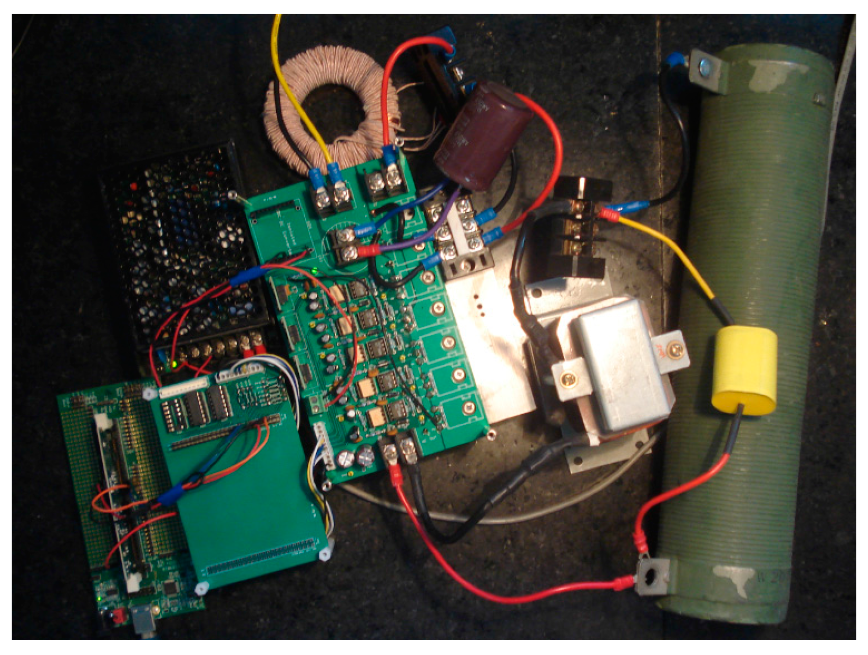
Two 700 W prototypes were used to verify the operating principle of the single-phase improved qSBI in Figure 5b and qZSI in Figure 1. The experimental parameters are listed in Table 1. A 61604 Chroma Programmable AC Source was used to supply the DC input voltage of 120 V. Power MOSFETs IRFP460 (Fairchild, Sunnyvale, CA, USA) and power diode DSEP30-06A (Ixys, Milpitas, CA, USA) were used. The PWM control signals for power switches were generated from a TMS320F28335 DSP (Texas Instruments, Dallas, TX, USA). Logic OR gates were used to insert the shoot-through state into switches S1 to S4. The switches were driven by isolated amplifiers (TLP250, Toshiba, Tokyo, Japan). Figure 7 shows an experimental prototype in the laboratory.
First, we tested the operating states of the single-phase improved SBI when Da is replaced by S6 and the small signal perturbation of the shoot-through duty cycle is ignored. When ignoring the small signal perturbation of the shoot-through duty cycle, the proposed maximum boost PWM control method was concluded with the simple boost control method. Figure 8 shows the experimental results for a qSBI when M = 0.8 and A = 0. When A = 0, the calculated shoot-through duty cycle was 0.2. Compared to Figure 4 we can see in Figure 8 that the DC-link voltage is constant during the non-shoot-through state, the 2ω inductor current ripple is significantly reduced, and the THD of the load current is decreased to 1.0% from 5.2% in Figure 4c. The DC-link voltage was boosted to 192 V from the 120 V input voltage. This value was close to the calculated value of 200 V when D = 0.2. The measured RMS output current was 4.8 A.
Next, small signal perturbation with a frequency of 100 Hz was injected into the shoot-through duty cycle. Figure 9 shows the experimental results for the improved SBI when M = 0.8 and A = 0.01. The shoot-through duty cycle calculated using Equation (6) was 0.21. The measured DC-link voltage is 200 V, which was close to the calculated value of 207 V when D = 0.21. The measured RMS output current and its THD were 5 A and 1.1%, respectively.
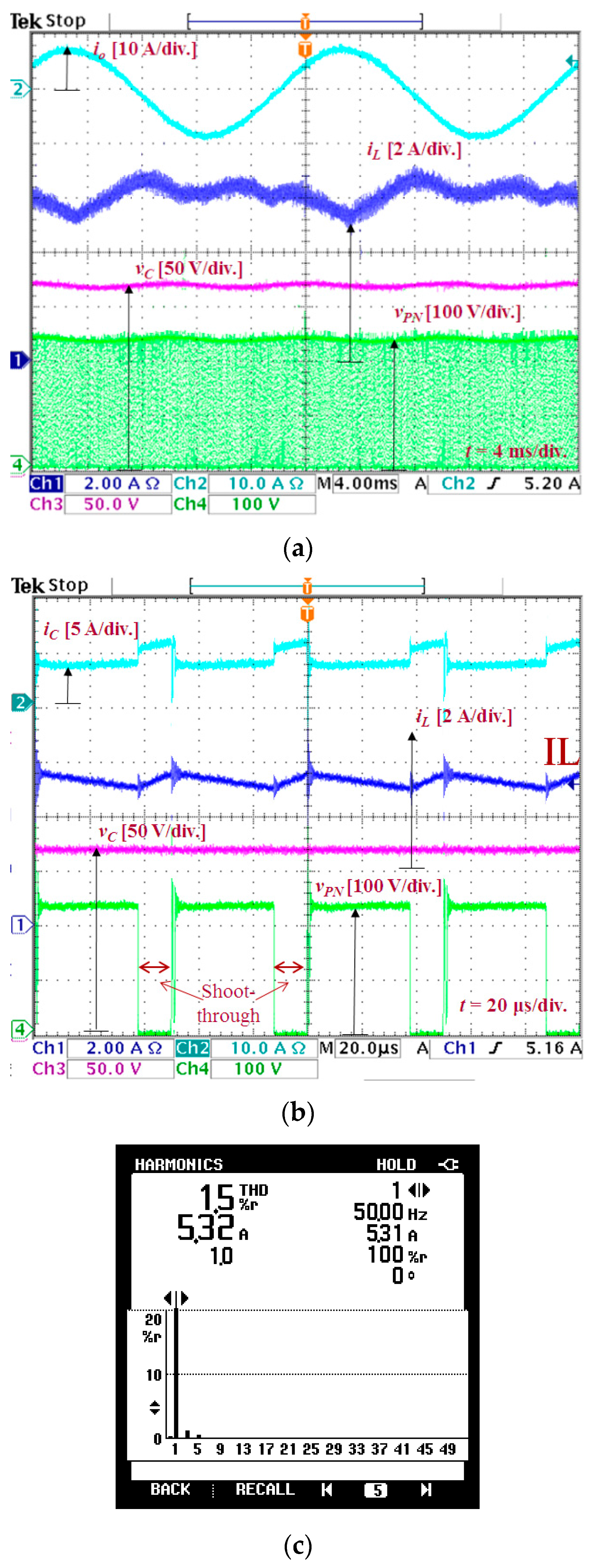
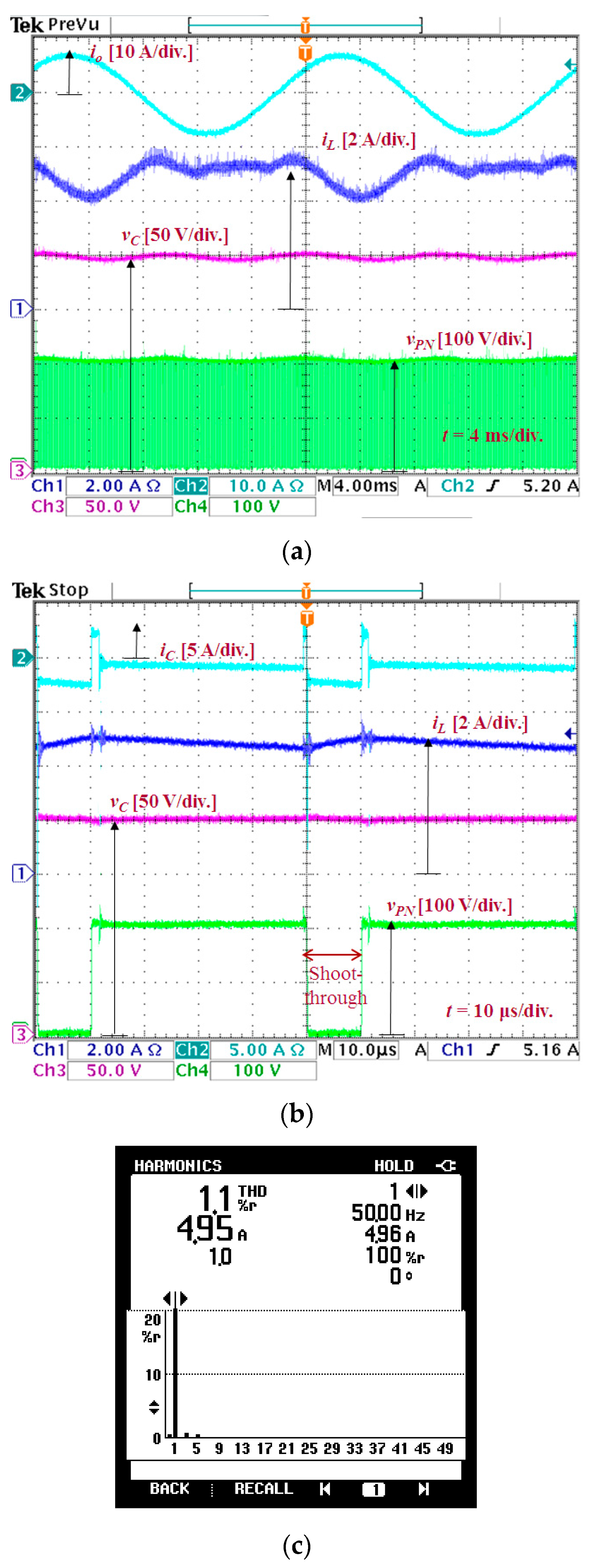
Then, the inverter was reconfigured as per the single-phase qZSI to test the proposed PWM strategy. Figure 10 shows the experimental results for the qZSI when M = 0.75 and A = 0.01. The calculated shoot-through duty cycle was 0.26. The measured DC-link voltage was 240 V, which was close to the calculated value of 250 V when D = 0.26. The measured RMS output current and its THD were 5.32 A and 1.5%, respectively.
Finally, we evaluated the 2ω voltage and current ripples and compared them to theoretical values. Table 2 shows the theoretical and experimental results of the amplitudes of 2ω voltage and current ripples with some errors. When the maximum boost control method was used, the 2ω inductor current ripple increased while the 2ω capacitor voltage ripple was incremented by a small amount.
6. Conclusions
The maximum boost control method for single-phase SBIs and single-phase ZSIs was proposed in this paper. In the proposed method, a low frequency voltage was added to the constant voltage to generate the variable shoot-through time intervals. An active power switch was used to replace one of the diodes of the single-phase SBI to improve the AC output quality of the inverter. The operating principles and circuit analysis performed using the proposed maximum boost control method for single-phase inverters were presented. Laboratory prototypes were built to verify the operation of the proposed PWM control method for both single-phase qZSIs and single-phase qSBIs.
Acknowledgments
This study was supported by research fund from Chosun University, 2016.
Author Contributions
Minh-Khai Nguyen conducted experimental work, data analysis and calculations. Youn-Ok Choi discussed the results and revised the whole work.
Conflicts of Interest
The authors declare no conflict of interest.
References
- Peng, F.Z. Z-source inverter. IEEE Trans. Ind. Appl. 2003, 39, 504–510. [Google Scholar] [CrossRef]
- Peng, F.Z.; Shen, M.; Qian, Z. Maximum boost control of the Z-source inverter. IEEE Trans. Power Electron. 2005, 20, 833–838. [Google Scholar] [CrossRef]
- Shen, M.; Wang, J.; Joseph, A.; Peng, F.Z.; Tolbert, L.M.; Adams, D.J. Constant boost control of the Z-source inverter to minimize current ripple and voltage stress. IEEE Trans. Ind. Appl. 2006, 42, 770–778. [Google Scholar] [CrossRef]
- Nguyen, M.K.; Lim, Y.C.; Cho, G.B. Switched-inductor quasi-Z-source inverter. IEEE Trans. Power Electron. 2011, 26, 3183–3191. [Google Scholar] [CrossRef]
- Loh, P.C.; Vilathgamuwa, D.M.; Gajanayake, G.J.; Lim, Y.R.; Teo, C.W. Transient modeling and analysis of pulse-width modulated Z-source inverter. IEEE Trans. Power Electron. 2007, 22, 498–507. [Google Scholar] [CrossRef]
- Jung, J.W.; Keyhani, A. Control of a fuel cell based Z-source converter. IEEE Trans. Energy Convers. 2007, 22, 467–476. [Google Scholar] [CrossRef]
- Liu, Y.; Ge, B.; Abu-Rub, H.; Peng, F.Z. Overview of space vector modulations for three-phase Z-source/quasi-Z-source inverters. IEEE Trans. Power Electron. 2014, 29, 2098–2108. [Google Scholar] [CrossRef]
- Ellabban, O.; van Mierlo, J.; Lataire, P. Comparison between different PWM control methods for different Z-source inverter topologies. In Proceedings of the 13th European Conference on Power Electronics and Applications (EPE’09), Barcelona, Spain, 8–10 September 2009; pp. 1–11. [Google Scholar]
- Zhou, Z.J.; Zhang, X.; Xu, P.; Shen, W.X. Single-phase uninterruptible power supply based on Z-source inverter. IEEE Trans. Ind. Electron. 2008, 55, 2997–3004. [Google Scholar] [CrossRef]
- Zhou, Y.; Liu, L.; Li, H. A high performance photovoltaic module-integrated converter (MIC) based on cascaded quasi-Z-source inverters (qZSI) using eGaN FETs. IEEE Trans. Power Electron. 2013, 28, 2727–2738. [Google Scholar] [CrossRef]
- Yu, Y.; Zhang, Q.; Liang, B.; Cui, S. Single-phase Z-source inverter: Analysis and low-frequency harmonics elimination pulse width modulation. In Proceedings of the IEEE Energy Conversion Congress and Exposition (ECCE), Phoenix, AZ, USA, 17–22 September 2011; pp. 2260–2267. [Google Scholar]
- Ge, B.; Liu, Y.; Abu-Rub, H.; Balog, R.S.; Peng, F.Z.; McConnell, S.; Li, X. Current Ripple Damping Control to Minimize Impedance Network for Single-Phase Quasi-Z Source Inverter System. IEEE Trans. Ind. Inform. 2016, 12, 1043–1054. [Google Scholar] [CrossRef]
- Zhou, Y.; Li, H.; Li, H. A single-phase PV quasi-Z-source inverter with reduced capacitance using modified modulation and double-frequency ripple suppression control. IEEE Trans. Power Electron. 2016, 31, 2166–2173. [Google Scholar] [CrossRef]
- Ge, B.; Abu-Rub, H.; Liu, Y.; Balog, R.S. An active filter method to eliminate dc-side low-frequency power for single-phase quasi-Z source inverter. In Proceedings of the IEEE Applied Power Electronics Conference and Exposition (APEC), Charlotte, NC, USA, 15–19 March 2015; pp. 827–832. [Google Scholar]
- Sun, D.; Ge, B.; Yan, X.; Bi, D.; Zhang, H.; Liu, Y.; Abu-Rub, H.; Ben-Brahim, L.; Peng, F. Modeling, impedance design, and efficiency analysis of quasi-Z-source module in cascade multilevel photovoltaic power system. IEEE Trans. Ind. Electron. 2014, 61, 6108–6117. [Google Scholar] [CrossRef]
- Liu, Y.; Ge, B.; Abu-Rub, H.; Sun, D. Comprehensive modeling of single-phase quasi-Z-source photovoltaic inverter to investigate low-frequency voltage and current ripple. IEEE Trans. Ind. Electron. 2014, 62, 4194–4202. [Google Scholar] [CrossRef]
- Liu, Y.; Abu-Rub, H.; Ge, B. Hybrid pulsewidth modulated single-phase quasi-Z-source grid-tie Photovoltaic power system. In Proceedings of the IEEE Applied Power Electronics Conference and Exposition (APEC), Charlotte, NC, USA, 15–19 March 2015; pp. 1763–1767. [Google Scholar]
- Tang, Y.; Xie, S.; Ding, J. Pulsewidth modulation of Z-source inverters with minimum inductor current ripple. IEEE Trans. Ind. Electron. 2014, 61, 98–106. [Google Scholar] [CrossRef]
- Shen, M.; Peng, F.Z. Operation modes and characteristics of the Z-source inverter with small inductance or low power factor. IEEE Trans. Ind. Electron. 2008, 55, 89–96. [Google Scholar] [CrossRef]
- Nguyen, M.K.; Lim, Y.C.; Park, S.J. A comparison between single-phase quasi-Z-source and quasi-switched boost inverters. IEEE Trans. Ind. Electron. 2015, 62, 6336–6344. [Google Scholar] [CrossRef]
- Adda, R.; Ray, O.; Mishra, S.K.; Joshi, A. Synchronous-reference-frame-based control of switched boost inverter for standalone dc nanogrid applications. IEEE Trans. Power Electron. 2013, 28, 1219–1233. [Google Scholar] [CrossRef]
- Ravindranath, A.; Mishra, S.; Joshi, A. Analysis and PWM control of switched boost inverter. IEEE Trans. Ind. Electron. 2013, 60, 5593–5602. [Google Scholar] [CrossRef]
- Nguyen, M.K.; Le, T.V.; Park, S.J.; Lim, Y.C. A Class of Quasi-Switched Boost Inverters. IEEE Trans. Ind. Electron. 2015, 62, 1526–1536. [Google Scholar] [CrossRef]
- Nag, S.S.; Mishra, S. Current–Fed Switched Inverter. IEEE Trans. Ind. Electron. 2014, 61, 4680–4690. [Google Scholar] [CrossRef]
- Nguyen, M.K.; Le, T.V.; Park, S.J.; Lim, Y.C.; Yoo, J.Y. Class of high boost inverters based on switched-inductor structure. IET Power Electron. 2015, 8, 750–759. [Google Scholar] [CrossRef]
- Ho, A.V.; Chun, T.W.; Kim, H.G. Extended Boost Active-Switched-Capacitor/Switched-Inductor Quasi-Z-Source Inverters. IEEE Trans. Power Electron. 2015, 30, 5681–5690. [Google Scholar] [CrossRef]
Figure 1.
Single-phase quasi-Z-source inverter.
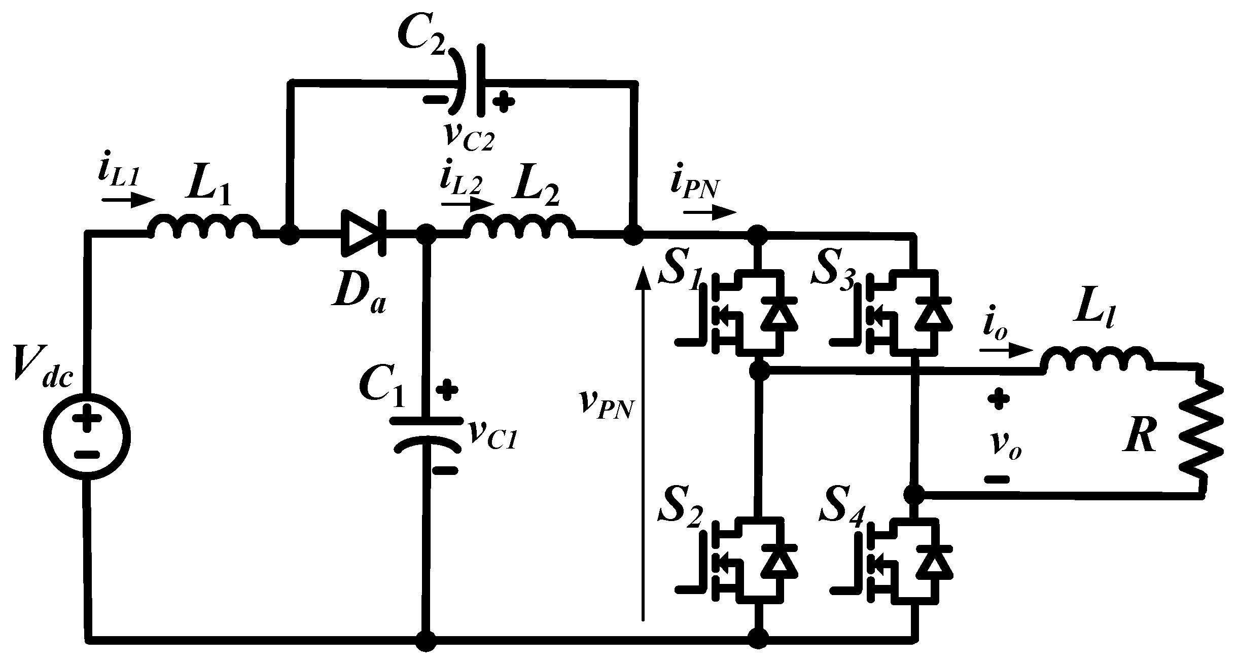
Figure 2.
Single-phase qSBIs (a) type 1 and (b) type 2.

Figure 3.
Operating states of qSBI type 2 under small shoot-through duty cycle; (a) shoot-through; (b) non-shoot-through when iL > iPN and (c) non-shoot-through when iL = iPN.
Figure 3.
Operating states of qSBI type 2 under small shoot-through duty cycle; (a) shoot-through; (b) non-shoot-through when iL > iPN and (c) non-shoot-through when iL = iPN.
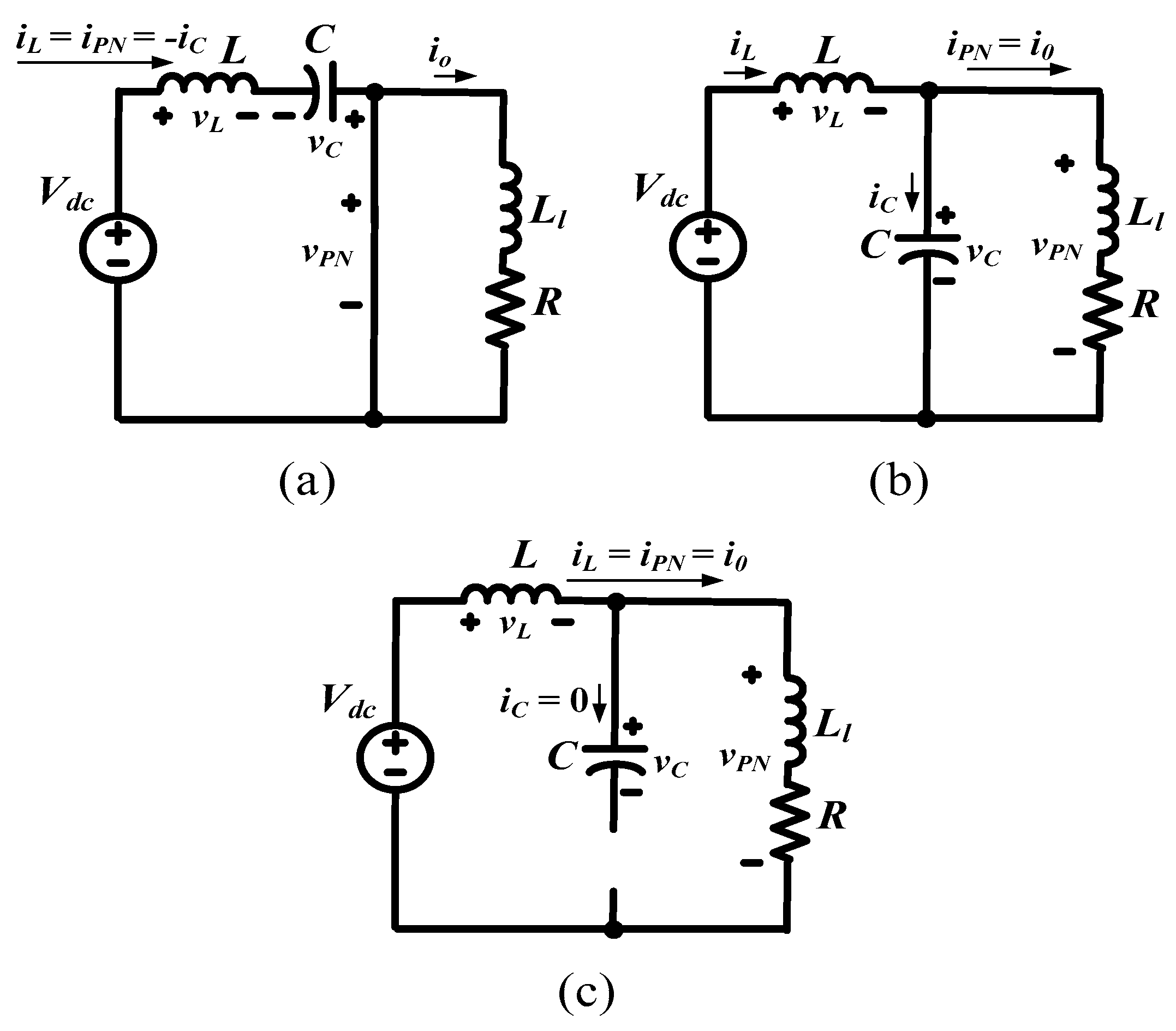
Figure 4.
Experimental waveforms for qSBI when Vdc = 120 V, D = 0.2, and M = 0.8. From top to bottom: (a) load current, inductor current, capacitor voltage, DC-link voltage; (b) capacitor current, capacitor voltage, inductor current, DC-link voltage; and (c) load current harmonics.
Figure 4.
Experimental waveforms for qSBI when Vdc = 120 V, D = 0.2, and M = 0.8. From top to bottom: (a) load current, inductor current, capacitor voltage, DC-link voltage; (b) capacitor current, capacitor voltage, inductor current, DC-link voltage; and (c) load current harmonics.


Figure 5.
Improved single-phase qSBIs; (a) type 1 and (b) type 2.
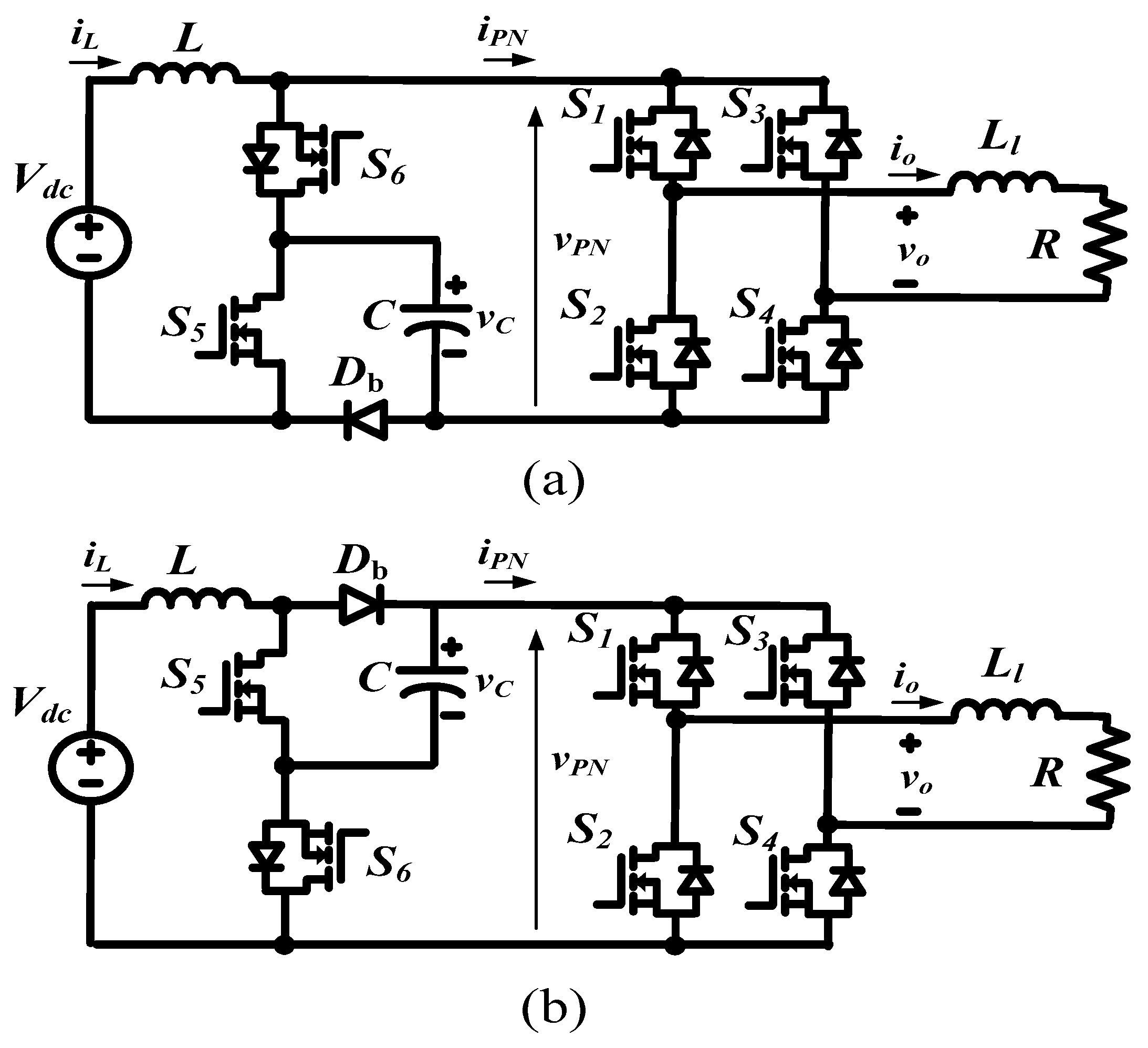
Figure 6.
Maximum boost control method for modulation index improvement.

Figure 7.
Experimental prototype in the laboratory.

Figure 8.
From top to bottom: (a) load current, inductor current, capacitor voltage, DC-link voltage; (b) capacitor current, capacitor voltage, inductor current, DC-link voltage; and (c) load current harmonics.
Figure 8.
From top to bottom: (a) load current, inductor current, capacitor voltage, DC-link voltage; (b) capacitor current, capacitor voltage, inductor current, DC-link voltage; and (c) load current harmonics.
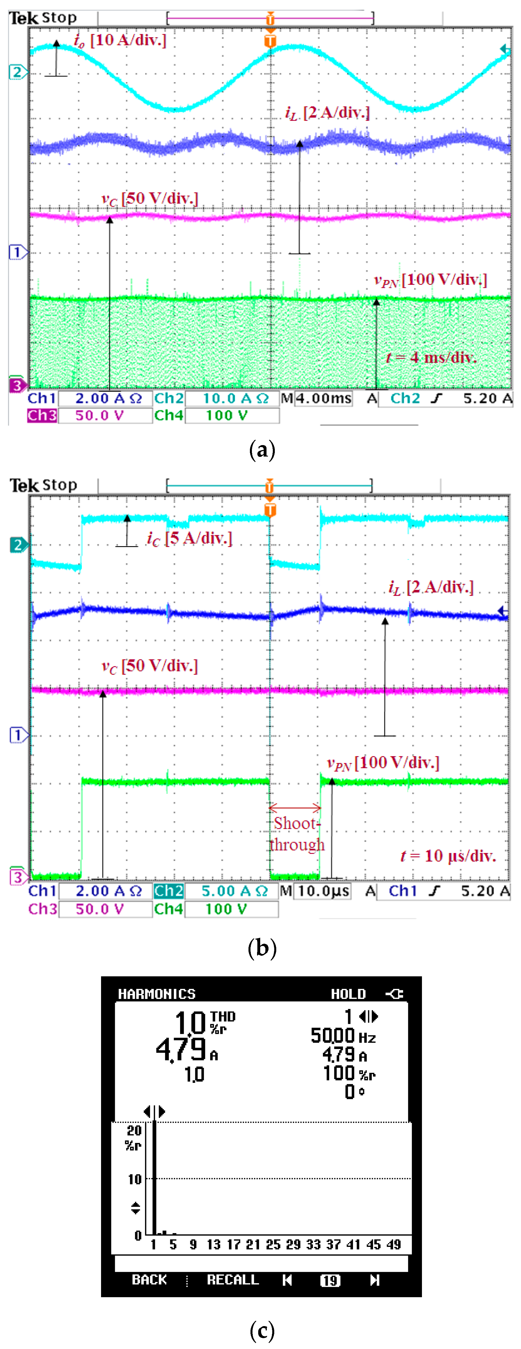
Figure 9.
Experimental waveforms for qSBI when Vdc = 120 V, M = 0.8 and A = 0.01. From top to bottom: (a) load current, inductor current, capacitor voltage, DC-link voltage; (b) capacitor current, capacitor voltage, inductor current, DC-link voltage; and (c) load current harmonics.
Figure 9.
Experimental waveforms for qSBI when Vdc = 120 V, M = 0.8 and A = 0.01. From top to bottom: (a) load current, inductor current, capacitor voltage, DC-link voltage; (b) capacitor current, capacitor voltage, inductor current, DC-link voltage; and (c) load current harmonics.

Figure 10.
Experimental waveforms for a qZSI when Vdc = 120 V, M = 0.75, and A = 0.01. From top to bottom: (a) load current, inductor current, capacitor voltage, DC-link voltage; (b) capacitor current, capacitor voltage, inductor current, DC-link voltage; and (c) load current harmonics.
Figure 10.
Experimental waveforms for a qZSI when Vdc = 120 V, M = 0.75, and A = 0.01. From top to bottom: (a) load current, inductor current, capacitor voltage, DC-link voltage; (b) capacitor current, capacitor voltage, inductor current, DC-link voltage; and (c) load current harmonics.

Table 1.
Operating parameters for improved SBI and QZSI in the experiment.
| Parameters | Values | |
|---|---|---|
| Power rating, Po (W) | 700 | |
| Input dc voltage, Vdc (V) | 120 | |
| qSB network | L (Mh) | 6 |
| C (mF) | 2 | |
| qZS network | L1 = L2 (mH) | 3 |
| C1 = C2 (mF) | 4 | |
| Switching frequency, fsw (kHz) | 10 | |
| Output frequency, fo (Hz) | 50 | |
| Load | Ll (mH) | 5 |
| R (Ω) | 20 | |
Table 2.
Theoretical and experimental results of amplitudes of 2ω voltage and current ripples.
| Single-Phase Improved SBI | A = 0 | A = 0.01 | ||
| Cal. | Exp. | Cal. | Exp. | |
| iL (peak) | 0.38 A | 0.39 A | 0.79 A | 0.74 A |
| vC (peak) | 2.5 V | 2.6 V | 2.6 V | 2.8 V |
| Single-Phase qZSI | A = 0 | A = 0.01 | ||
| Cal. | Exp. | Cal. | Exp. | |
| iL (peak) | 0.39 A | 0.41 A | 0.78 A | 0.7 A |
| vC (peak) | 2.8 V | 3.0 V | 2.9 V | 3.2 V |
© 2017 by the authors. Licensee MDPI, Basel, Switzerland. This article is an open access article distributed under the terms and conditions of the Creative Commons Attribution (CC BY) license (http://creativecommons.org/licenses/by/4.0/).
Share and Cite
MDPI and ACS Style
Nguyen, M.-K.; Choi, Y.-O. Maximum Boost Control Method for Single-Phase Quasi-Switched-Boost and Quasi-Z-Source Inverters. Energies 2017, 10, 553. https://doi.org/10.3390/en10040553
AMA Style
Nguyen M-K, Choi Y-O. Maximum Boost Control Method for Single-Phase Quasi-Switched-Boost and Quasi-Z-Source Inverters. Energies. 2017; 10(4):553. https://doi.org/10.3390/en10040553
Chicago/Turabian StyleNguyen, Minh-Khai, and Youn-Ok Choi. 2017. "Maximum Boost Control Method for Single-Phase Quasi-Switched-Boost and Quasi-Z-Source Inverters" Energies 10, no. 4: 553. https://doi.org/10.3390/en10040553
Note that from the first issue of 2016, this journal uses article numbers instead of page numbers. See further details here.