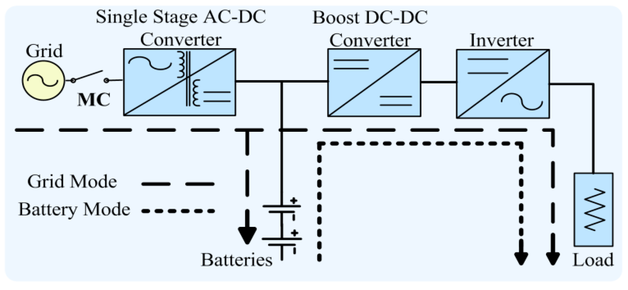
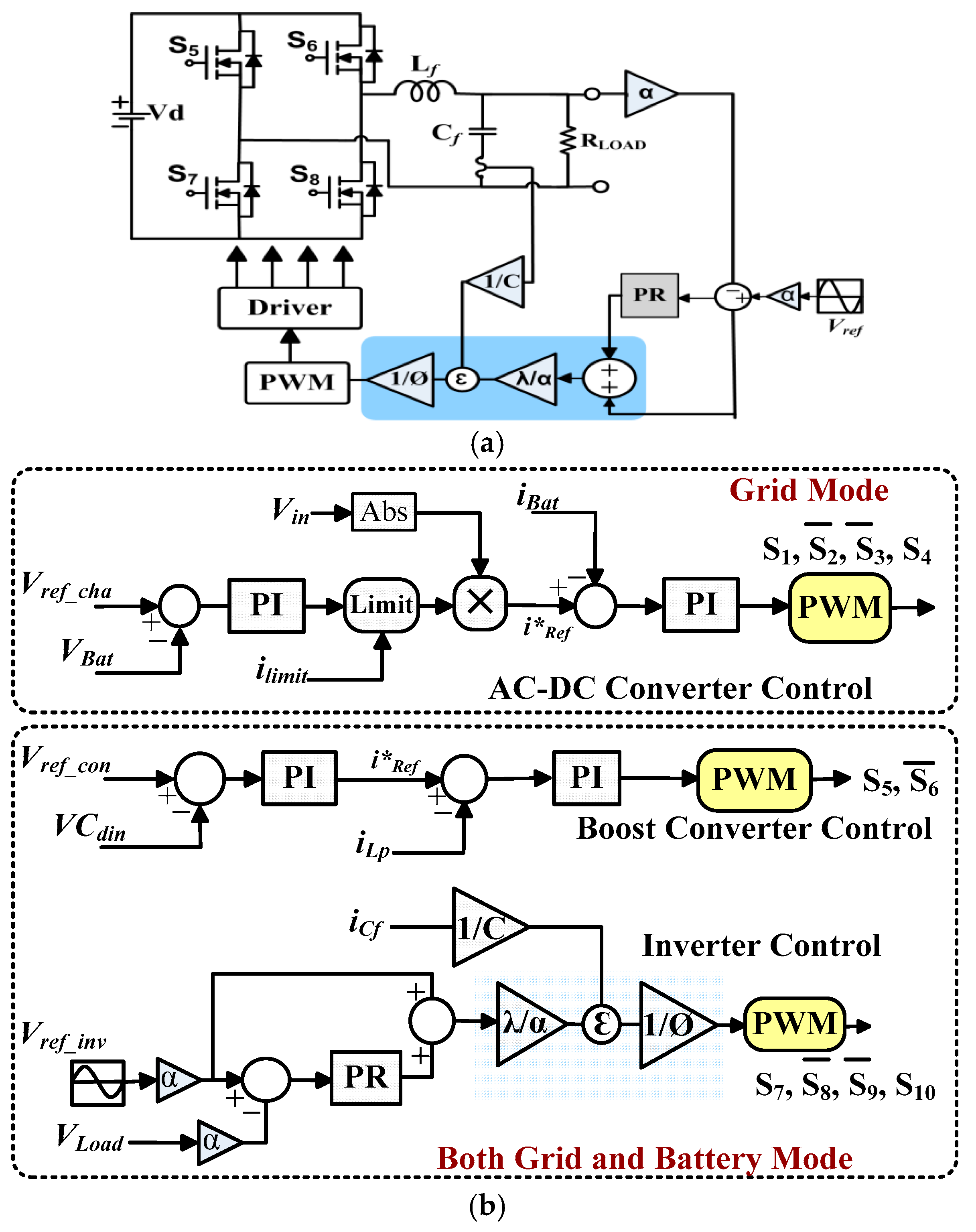
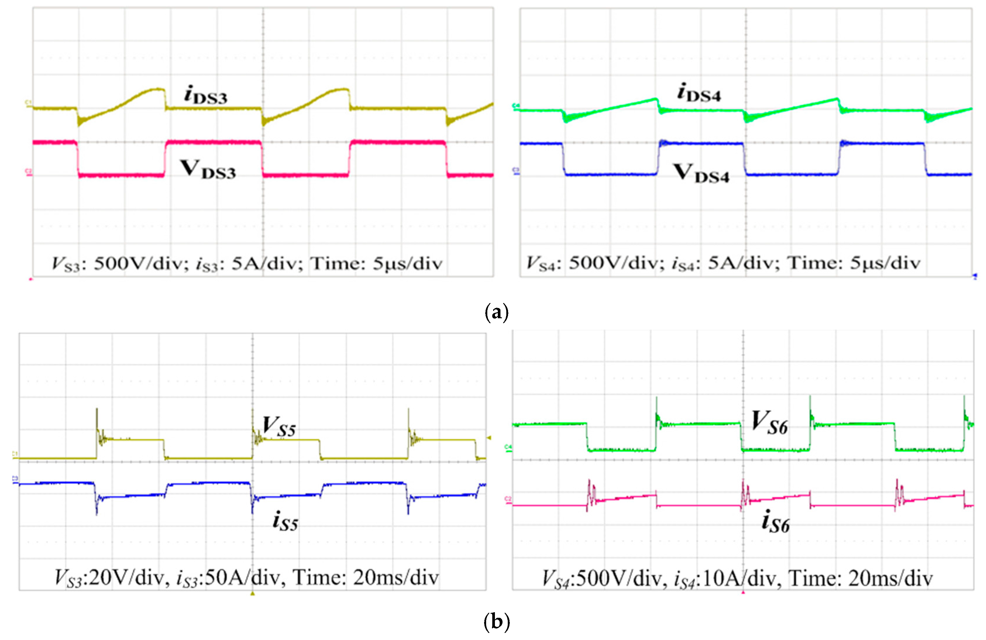
The control schemes for regulating different parts of the proposed UPS, in different modes of operation are shown in
Figure 5. The control scheme for inverter and boost converter keeps operating in both the normal and battery powered mode. On the other hand, for a single-stage converter the control scheme operates only in normal mode of operation for charging the battery as well as supplying power to the boost converter.
3.1. Inverter Control
A conventional full bridge voltage source inverter has been used to perform DC to AC conversion. SM control is famous for its excellent performance against non-linear loading conditions. SMC is also robust in operation and easy to implement for a full bridge inverter. In order to control the output voltage of the inverter, cascaded control algorithm of SMC and PR has been proposed for the control of inverter. The inner current loop is controlled by the SM control while the outer voltage loop is controlled by the PR control. Smoothed control law in narrow boundary layer has been used to eliminate the phenomena of chattering SMC. The smoothed control law is applied to the pulse width modulator that results in the fixed switching frequency of the inverter. Thus, the proposed controller adopted the characteristic of both SMC and PR control.
The circuit diagram of a single phase inverter with LC filter and proposed controller for non-linear load is shown in
Figure 5a, where
Vd is the applied DC-link voltage,
Vout the filter capacitor
Cf output voltage.
iLf is the inductor
Lf current and
io the output current through the load
R, given by
io =
Vout/
RLoad. The state equations of the inverter are given as:
where
.
In order to implement the sliding mode control, the voltage error
x1, and its derivative
need to be find:
where
. Consider the slide surface equation:
Now to apply the sliding control law to the inverter, putting the value of
x1 and
x2:
The sliding mode controller has the common inherent property of chattering. Chattering affects the control accuracy and reduces the efficiency of the circuit. In order to overcome the chattering, a smoothed SM control has been implemented. This can be achieved by smoothing out the control discontinuity in a thin boundary layer neighboring the sliding surface:
where
is the boundary layer thickness and
is the boundary layer width. Hence, interpolating
S inside
, for instance, and replacing
S by an expression
S/
, Equation (26) will be:
The smoothing control discontinuity assigns a low pass filter structure to the local dynamics thus eliminating chattering. The control law needs to be tuned very precisely in order to achieve a trade-off between the tracking precision and robustness to the uncontrolled dynamics. Hence, the final equation for the control of the inverter can be derived by combining the proportional resonant control and SM control for the current loop:
Thus Equation (29) shows the dynamic behavior in both SM and PR compensator control. The error in the voltage loop is compensated by the appropriate PR parameters, thus, the output voltage is compelled to follow the reference AC voltage leading to system stability while the SMC drives the system to the zero sliding surface with maximum stability. Since the capacitor error current contains the ripples from the inductor, the current peak may reach high values, so should be carefully assigned a value in order to compensate the slope from the high current ripple of the capacitor. Hence, the PR controller eliminates the steady-state error at resonant frequency or harmonic at that frequency. The response time of the system determines the dynamics and robustness of the system. It is clear from Equation (29), that a smaller value of leads to a slow response time, while higher values though increase the response time, but take a longer time to reach the sliding surface. Thus the optimal value for is equal to the switching frequency of the inverter.
According to [
32], the slope of the carrier wave is
, where
is the magnitude and
fs is the frequency of carrier wave. The slope of the error signal to the modulator is given by
. According to the limitation of the pulse width modulator, slope of error signal < slope of the carrier signal:
Thus, the minimum value of
can be calculated using (30):
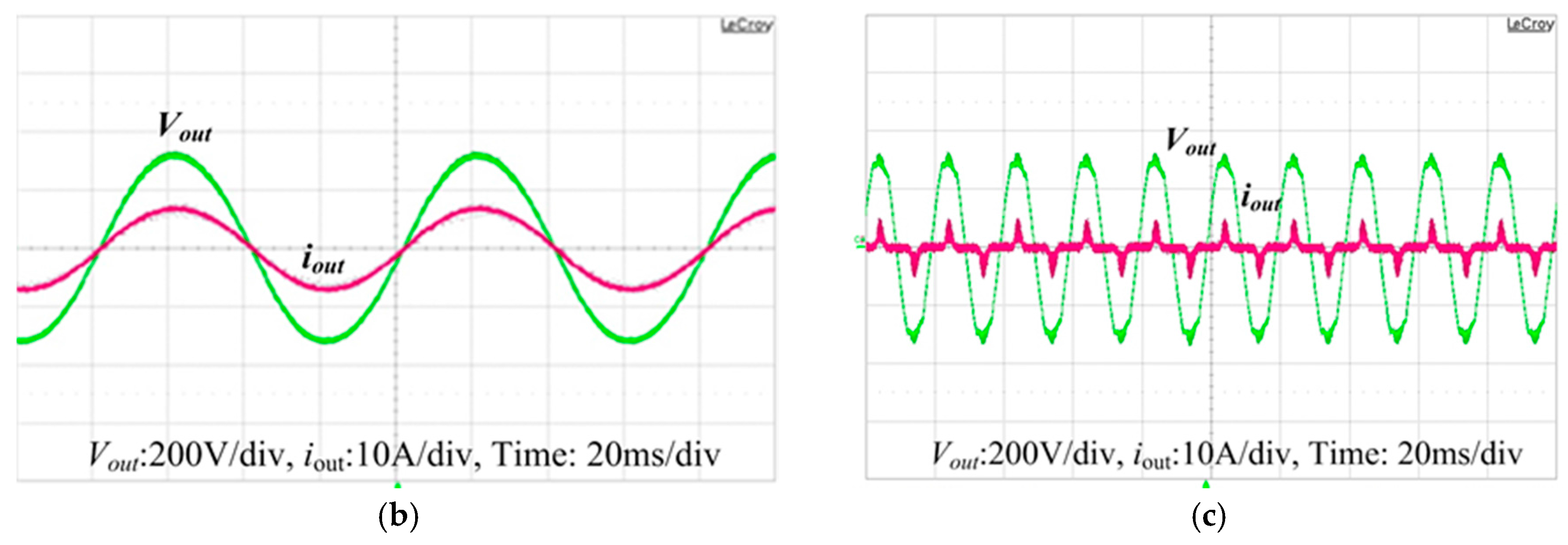
Table 2 shows the comparison of the proposed control scheme with the SM control and other common controllers. The proposed controller shows an improvement in terms of reducing the THD and transient response (
TS) with robust control of the inverter.
3.2. Battery Charger Control
The AC-DC converter of the UPS system acts as a battery charger as shown in
Figure 5. In this control scheme, the faster inner current loop regulates the inductor current so that its average value during each period follows the rectified input voltage. The slower outer voltage loop maintains the battery voltage close to reference voltage and generates the control signal for the current loop. The steady state analysis of the AC-DC converter shows stable performance during grid mode. The state space equations of the rectifier are derived as:
Assuming the current loop has high bandwidth as compared to the voltage loop, and dc-link capacitor
Cd is large enough to give approximately constant voltage i.e.,
. With
the small signal control
to input current
transfer function
of the inner current loop is give by:
The stability of the current loop depends on the current loop gain, hence a suitable proportional-integral (PI) controller
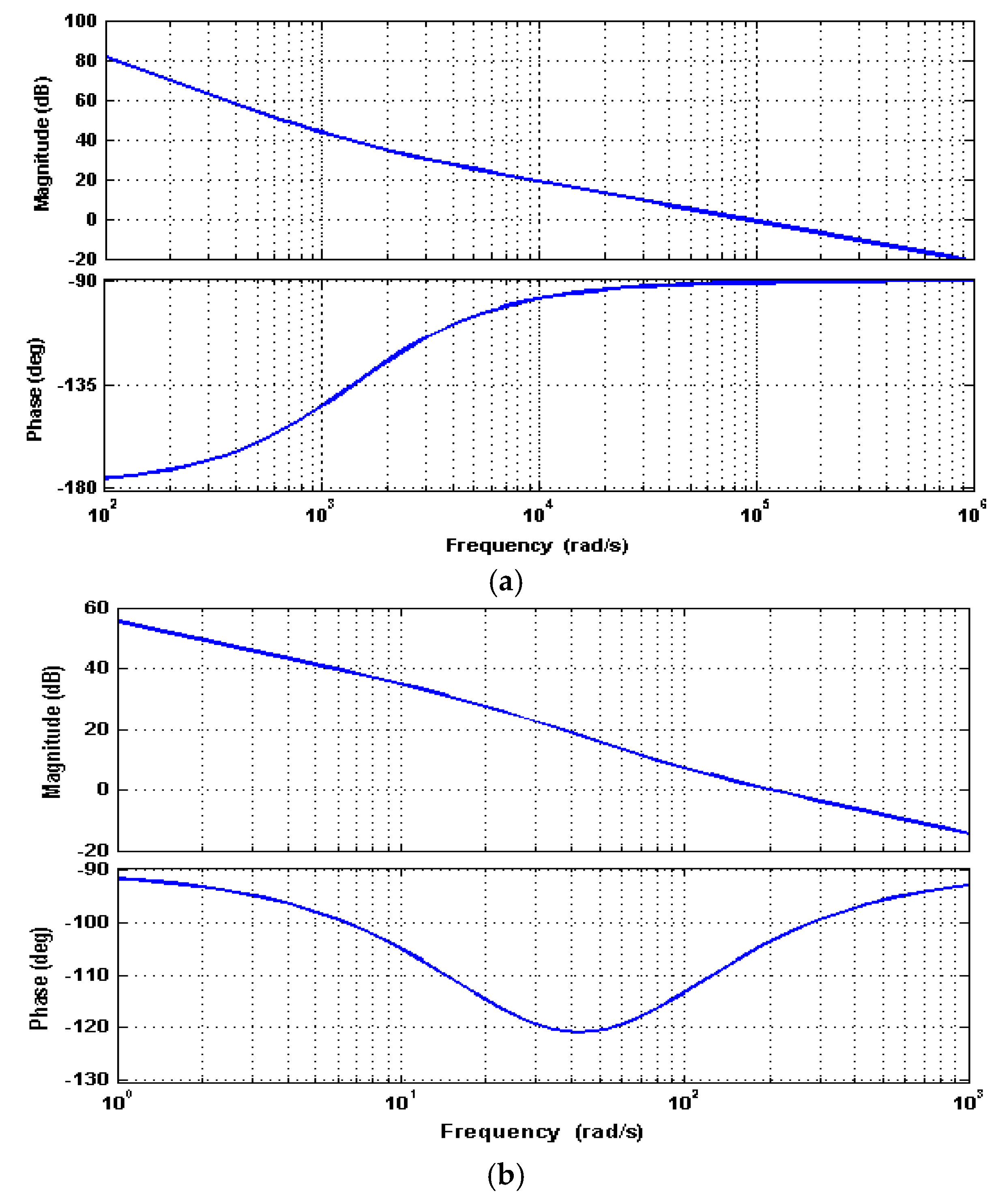
, is used for compensating the current loop. The Bode plot of the current loop gain
is obtained considering the circuit parameters shown in Table 4. The values of the proportional gain
Kpi and integral gain
Kii are selected as 2.3 and 1200, respectively, for the stable operation of the current loop.
Figure 6a presents the Bode plot of the current loop gain with phase margin of 89° and stable operation of the rectifier.
The same approach is used to compensate the voltage loop of the average current control scheme.
is the reference current for the current loop. Assuming constant input voltage, the small signal control
to output transfer function
of the voltage loop is derived as:
In order to force the output voltage to follow the reference voltage VRef, a proportional-integral (PI) compensator has been employed. Combining the power stage with the PI controller provides the overall loop gain.
of the voltage loop. The values of
Kpv and
Kiv in voltage loop are selected as 1.2 and 13, respectively. The stability of the voltage loop can be analyzed using the Bode plot obtained by considering the parameters from Table 4, as shown in
Figure 6b. The system shows good stability with a positive phase margin.
In charging mode, the controller operates as constant current mode CC or constant voltage mode CV depending on the battery voltage as shown in the
Figure 5b. In current loop, the battery input current
iBat is forced to follow the reference current
iRef using a PI compensator in (36):
Similarly, the battery voltage is regulated by the voltage loop using the PI compensator that forces the output battery voltage VBat to follow the reference voltage Vref. The current limiter is introduced to limit the maximum charging current of the battery. If the iref is greater than ilimit, the battery is charged at constant current (CC Mode), in contrast if the iref is less than ilimit, the battery is charged at constant voltage (CV mode).
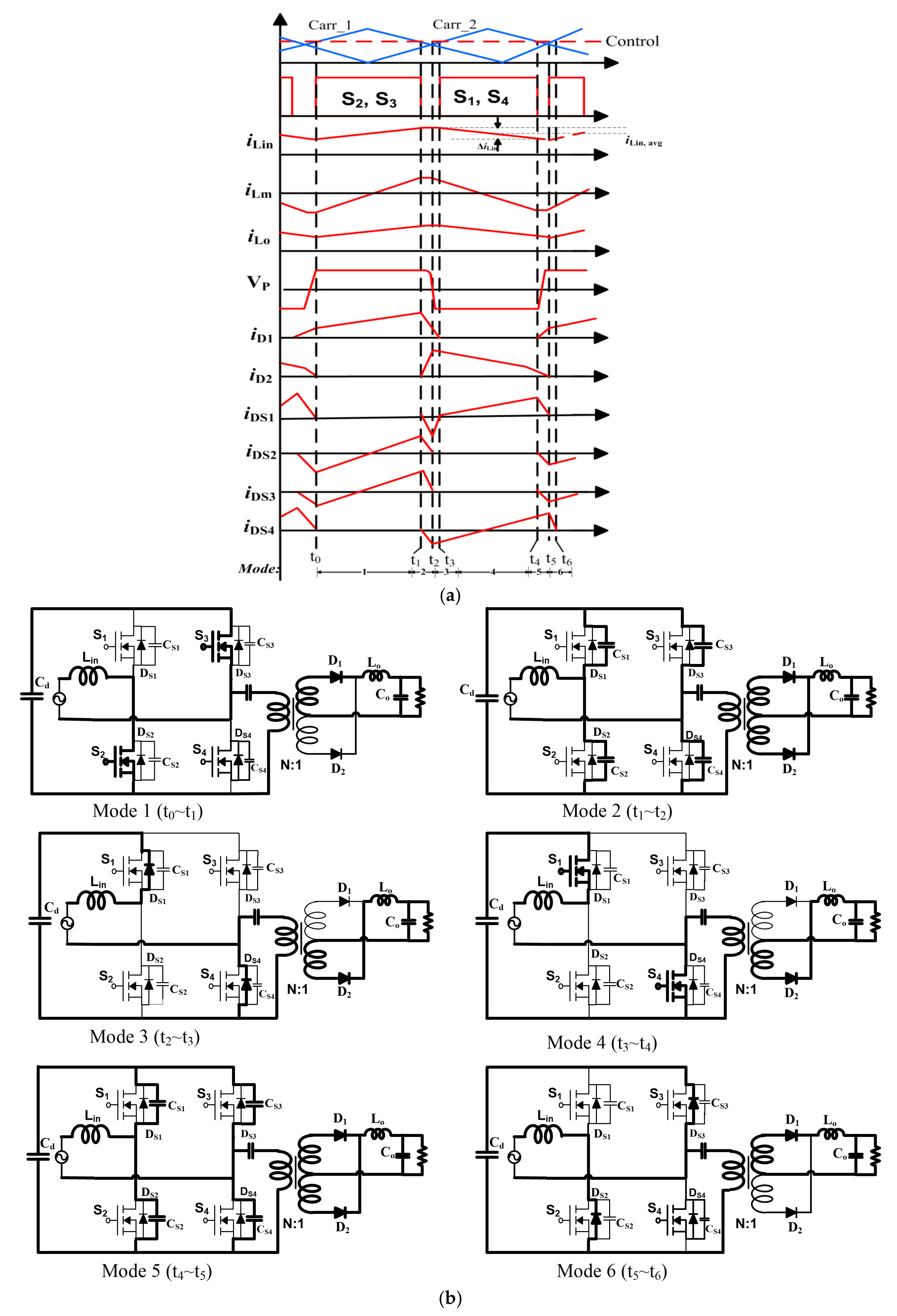
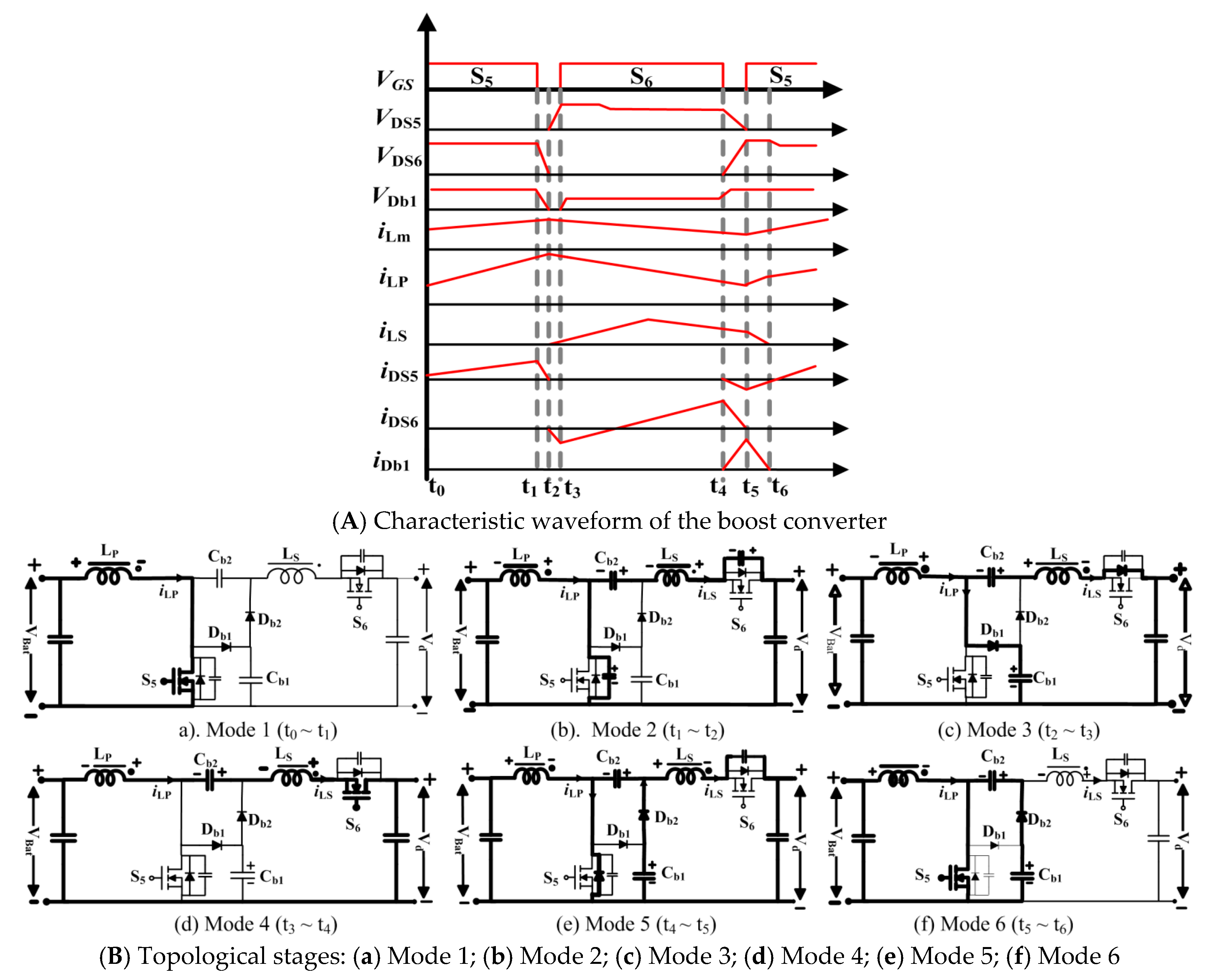
3.3. Boost Converter Control
The steady state analysis of the boost converter is performed using average state variable method [
30]. The state space equation for the converter with coupled inductor is derived as:
Now we perturb the system and consider only the dynamic terms and eliminate the product of the AC terms because of very small value. The final equation after Laplace transform is:
Solving (37) and (38) gives the transfer function of the converter:
Considering the gain due to clamp capacitor C
b2, the transfer equation is given by:
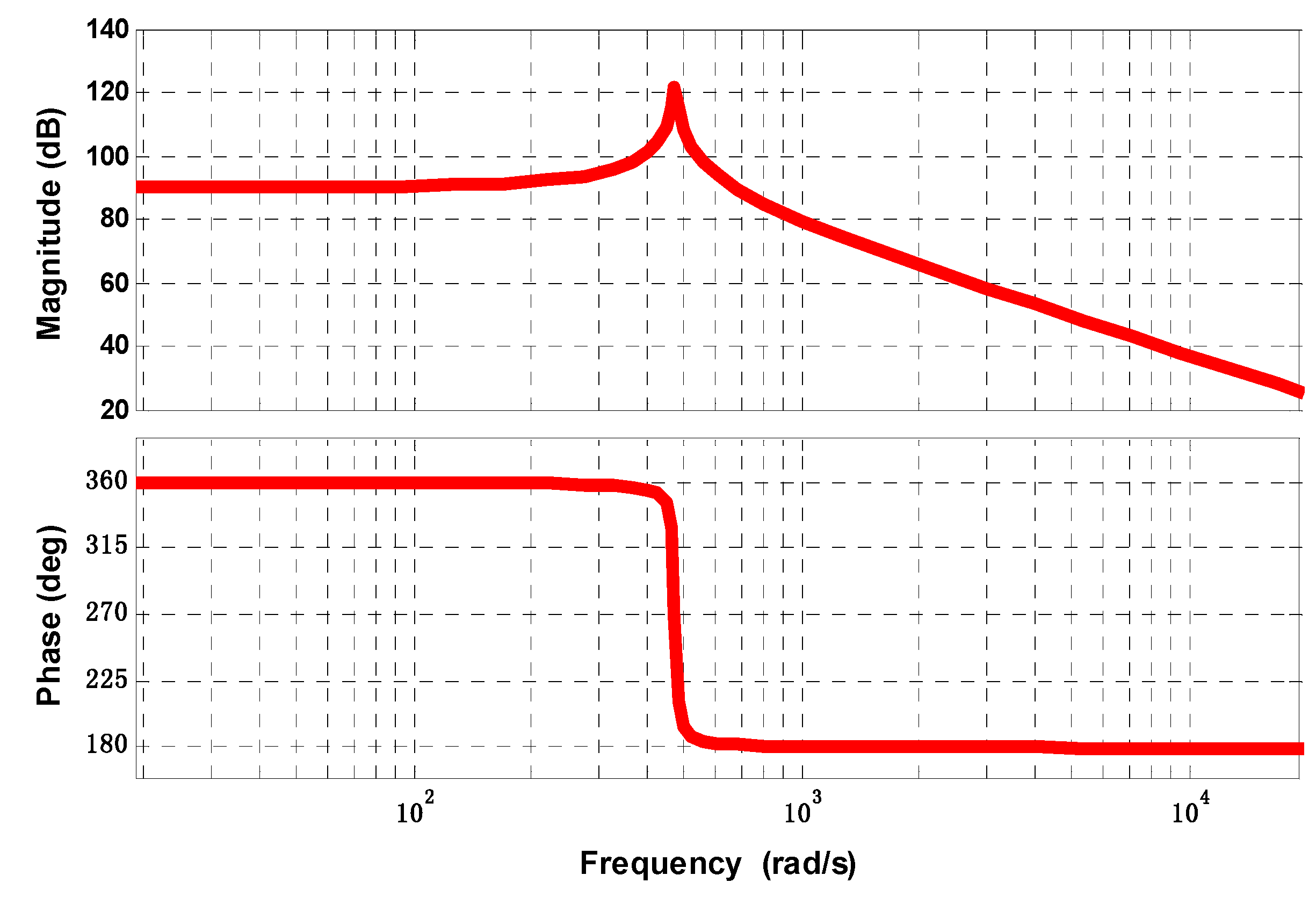
The stability of the converter can be analyzed using the Bode plot shown in
Figure 7. The system shows good stability with a positive phase margin and it has no right half plane poles. It is easy to achieve high crossover frequencies by adjusting a suitable gain of the compensators as the phase never reaches −180. The voltage across DC-link capacitor
Cdin is regulated by using a suitable voltage compensator [
37]. The PI compensator is used to track the DC-link voltage
Vd to follow the reference voltage, as shown in
Figure 7.


 ,
, 


