
A Digital Lock-In Amplifier for Use at Temperatures of up to 200 °C

Abstract
:1. Introduction
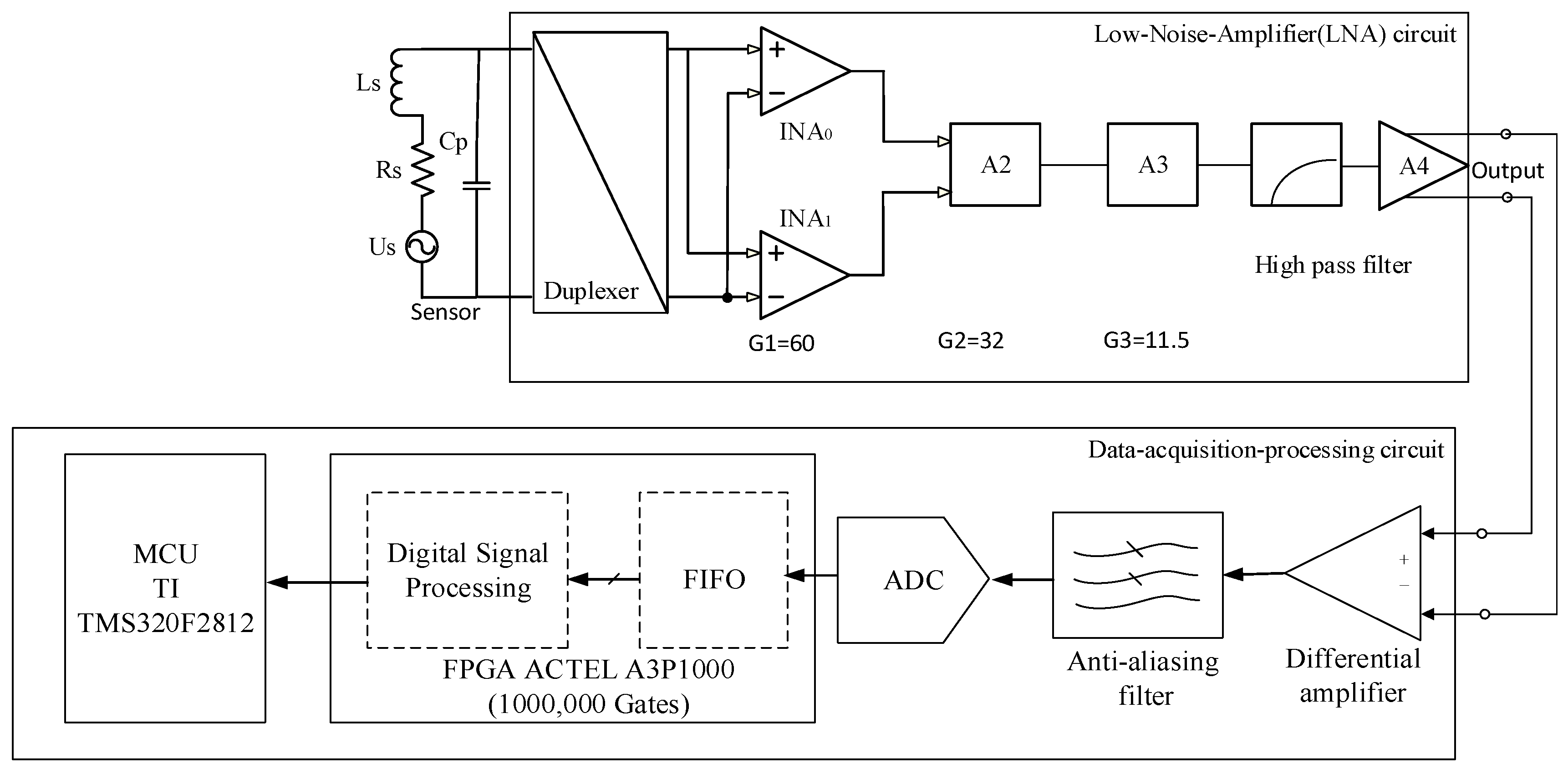
2. System Architecture
3. High Temperature DLIA
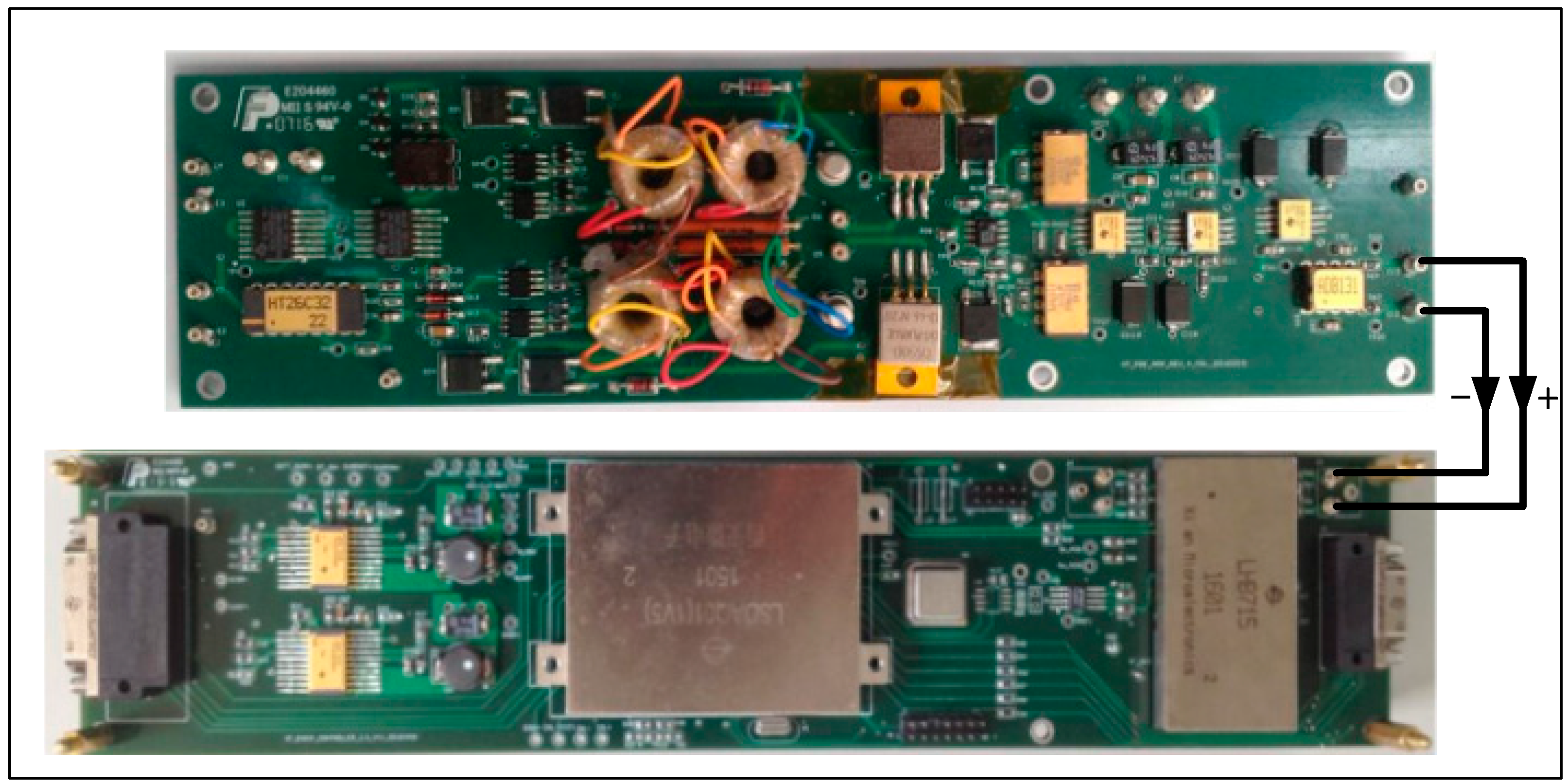
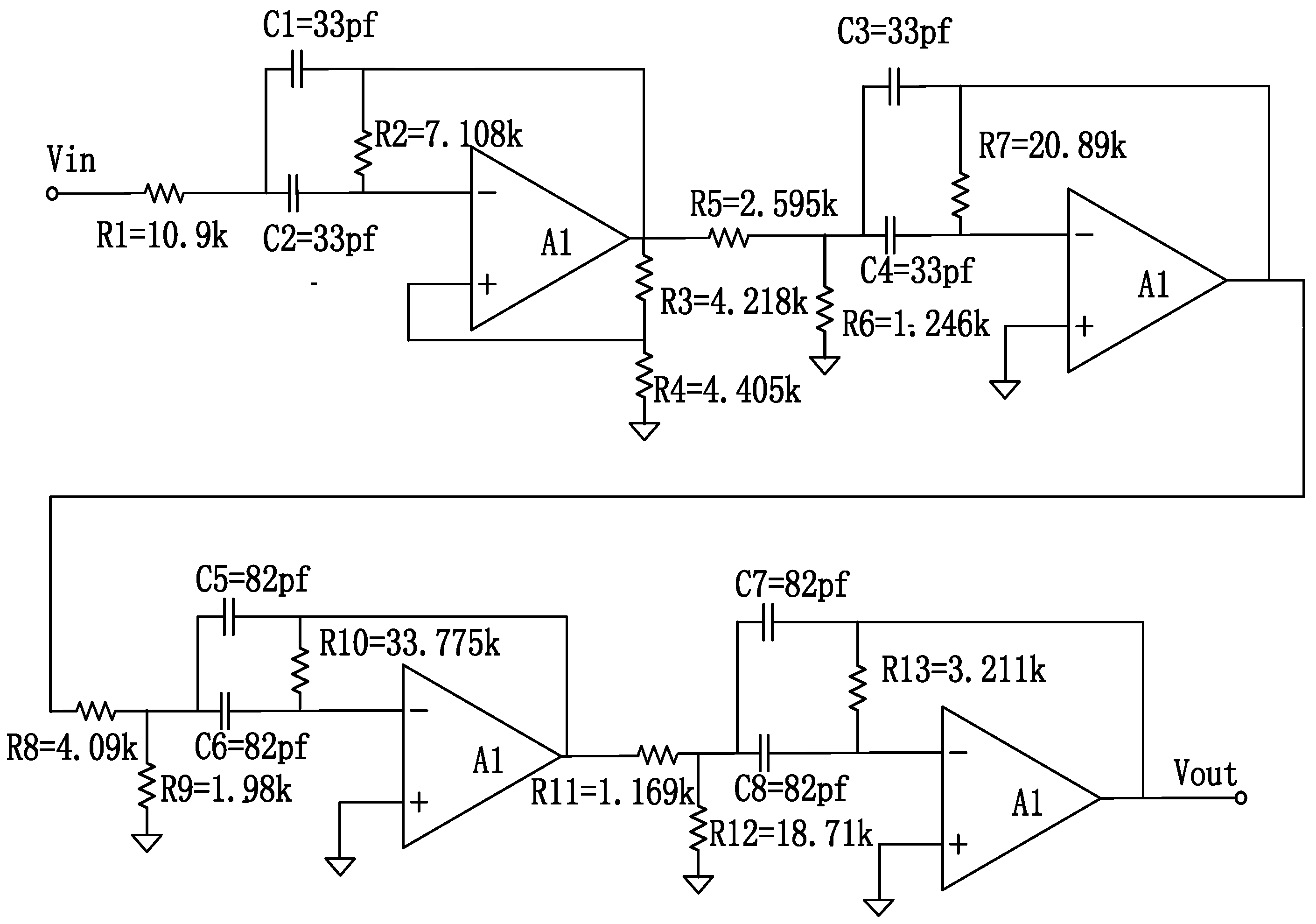
3.1. Low-Noise Amplifier
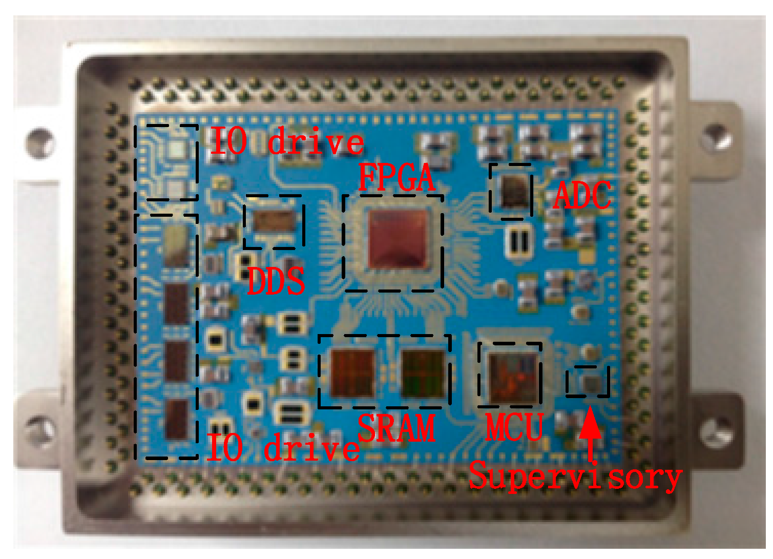
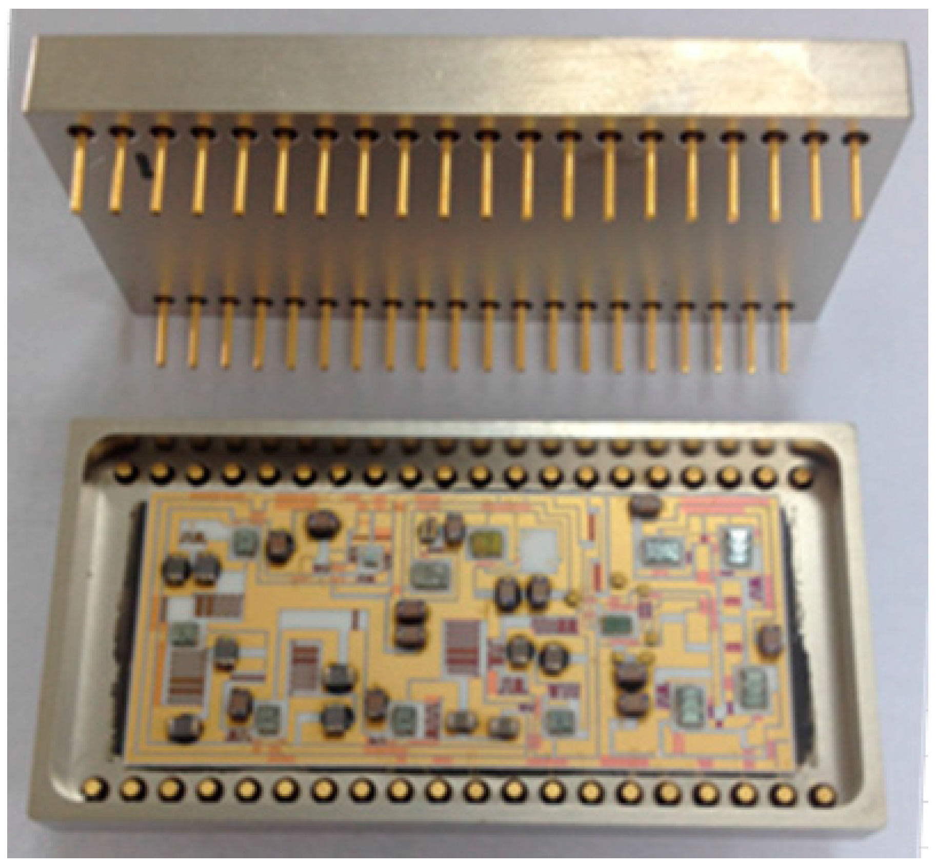
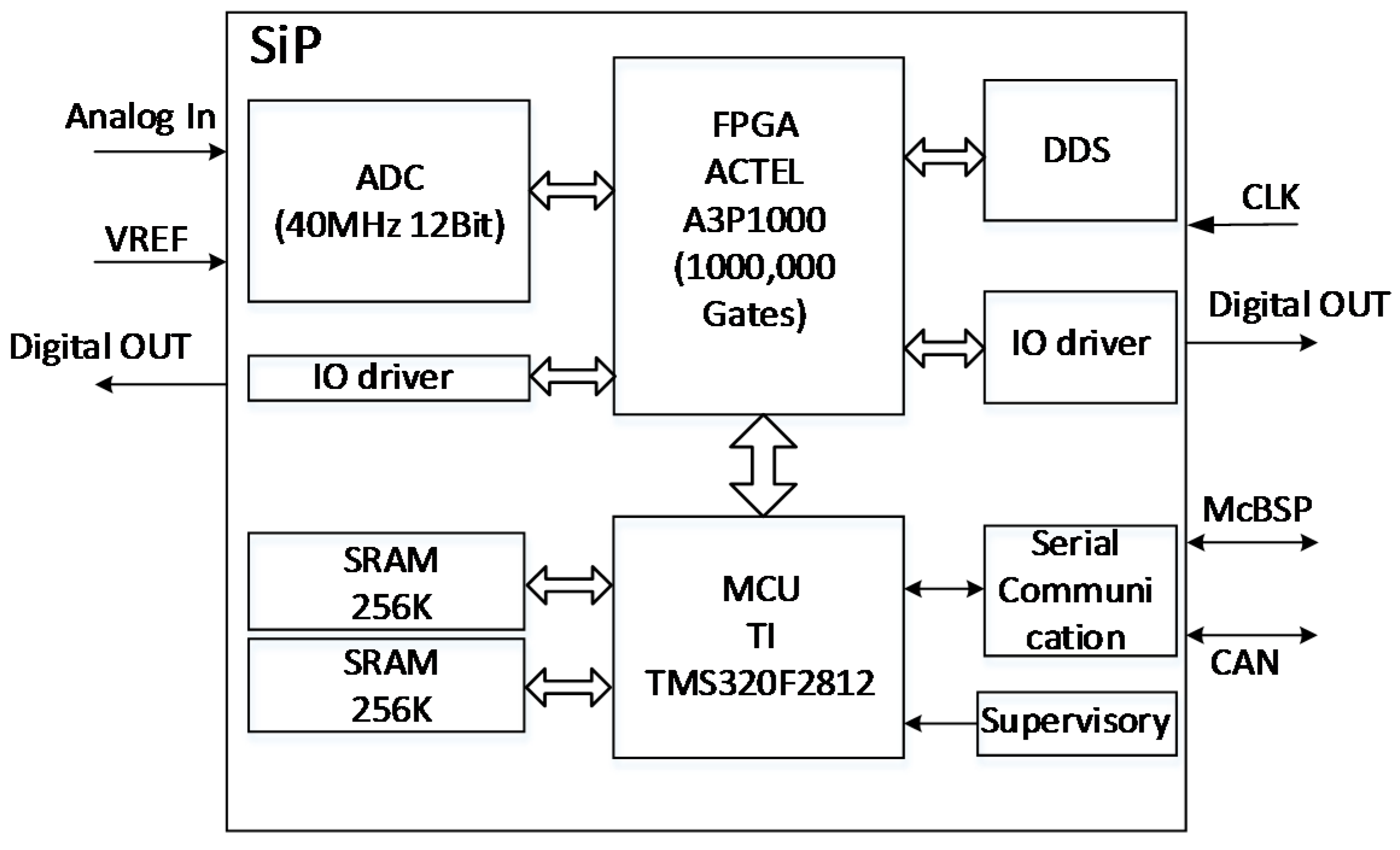
3.2. High-Speed Data Acquisition System-in-Package
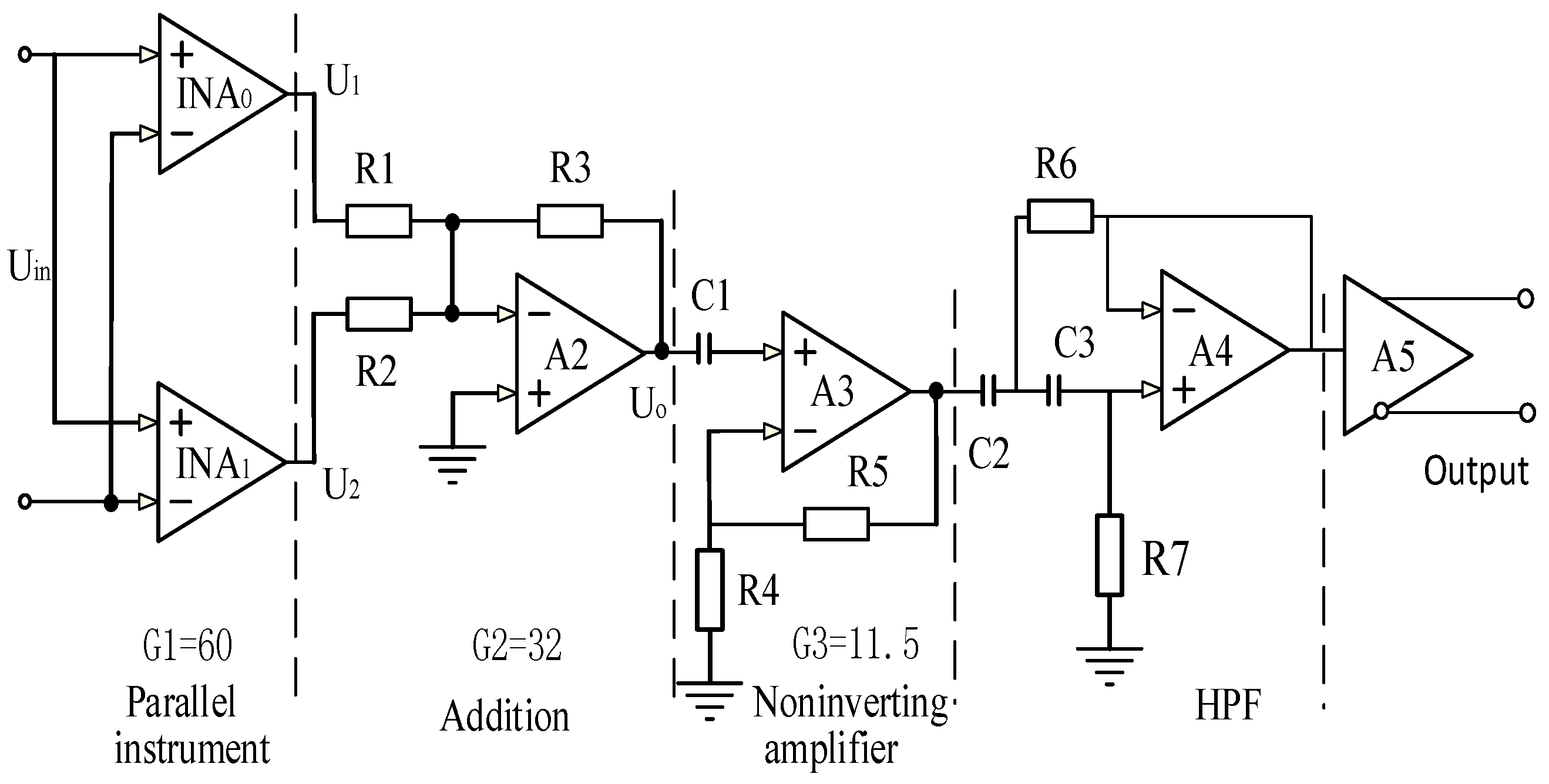
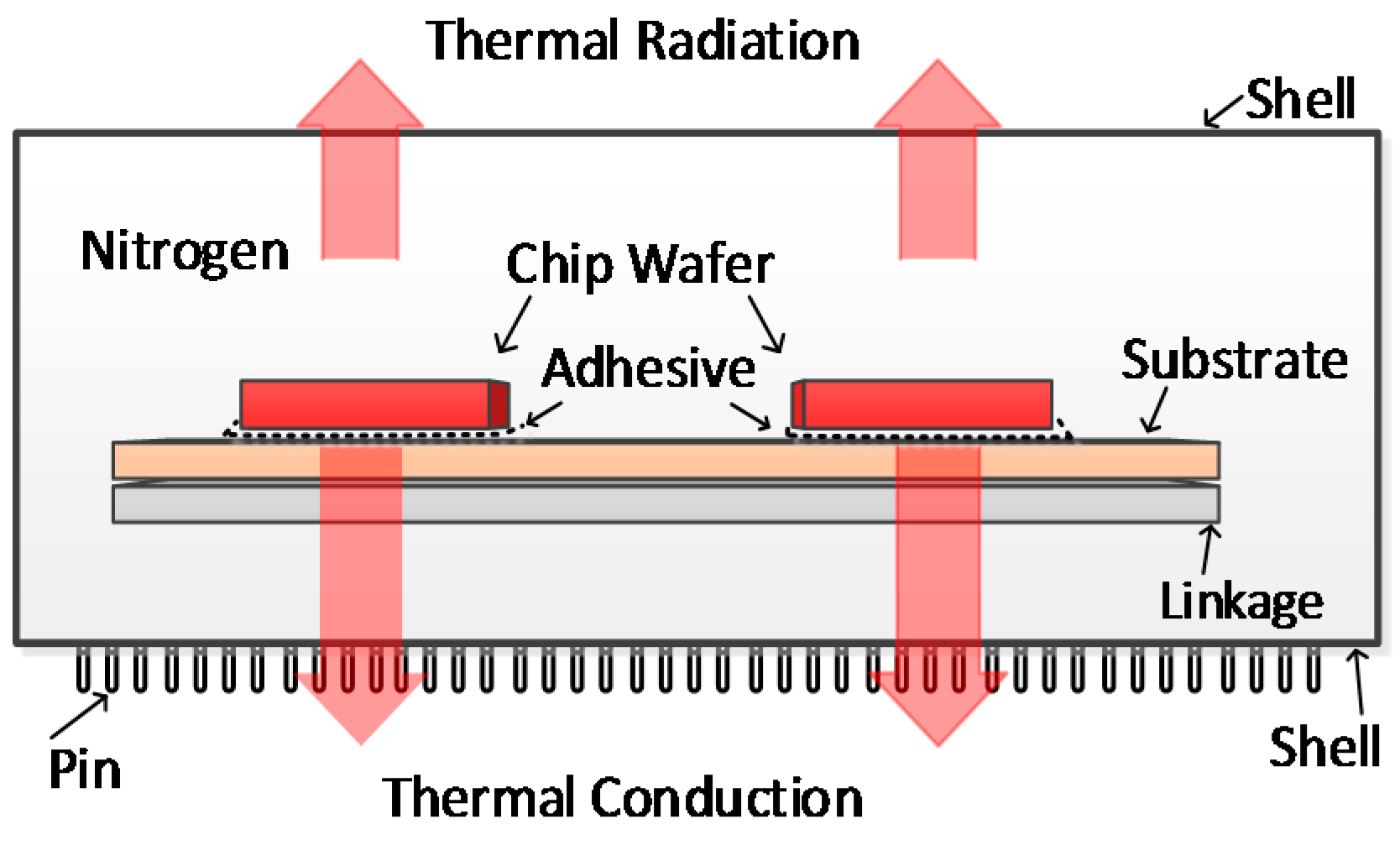
3.3. Signal Conditioning Multi-Chip Module
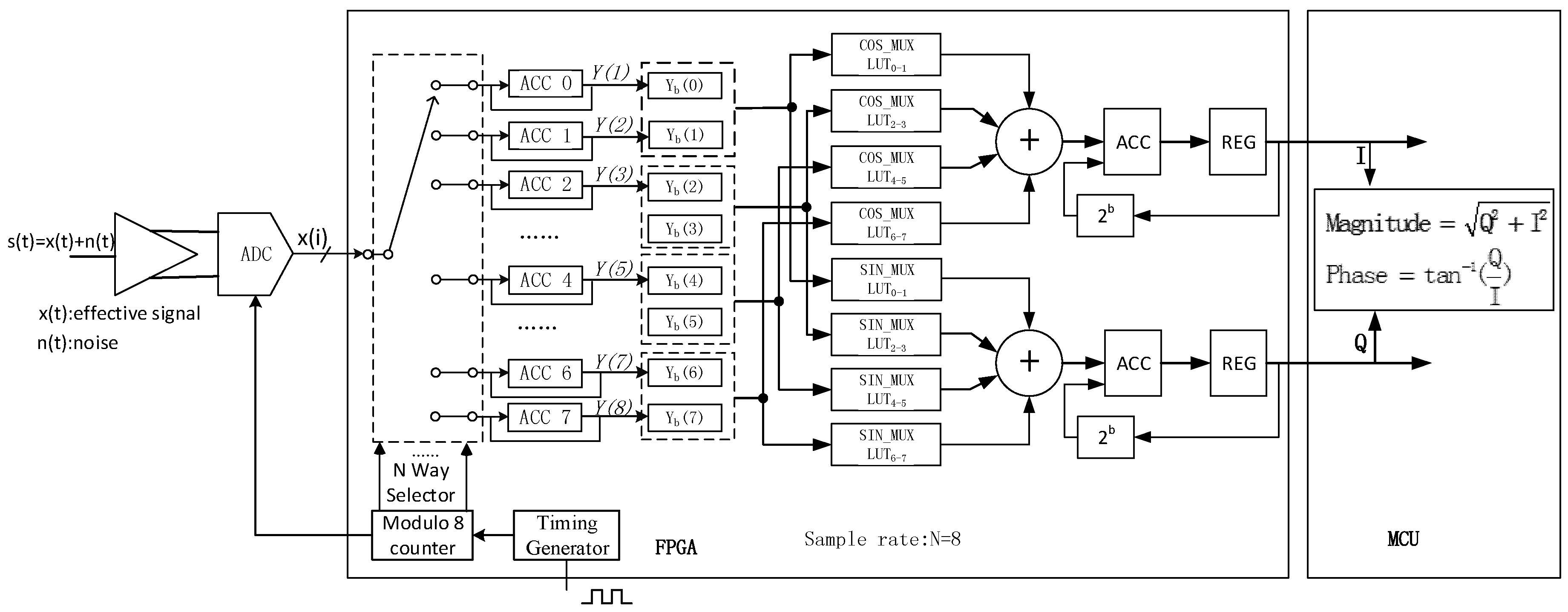
3.4. Digital Lock-In Algorithm for a Low-Field Nuclear Magnetic Resonance Logging Application
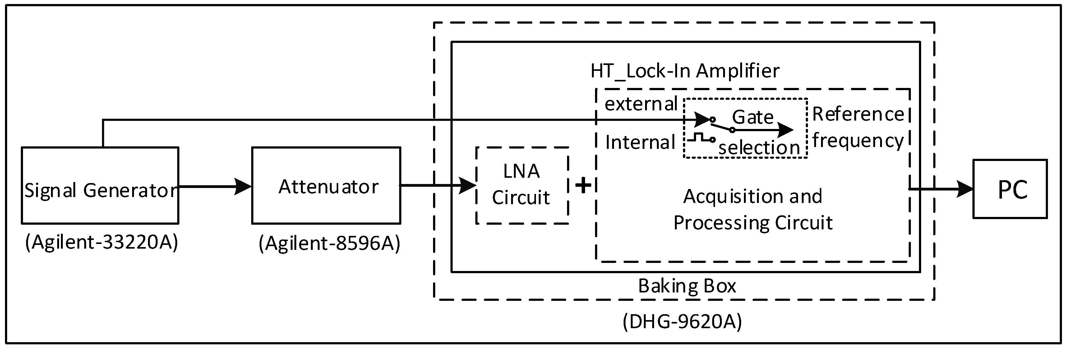
4. Experimental and Results
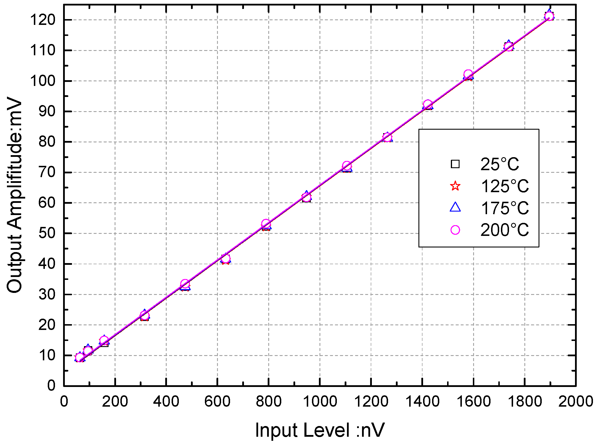
4.1. Linearity
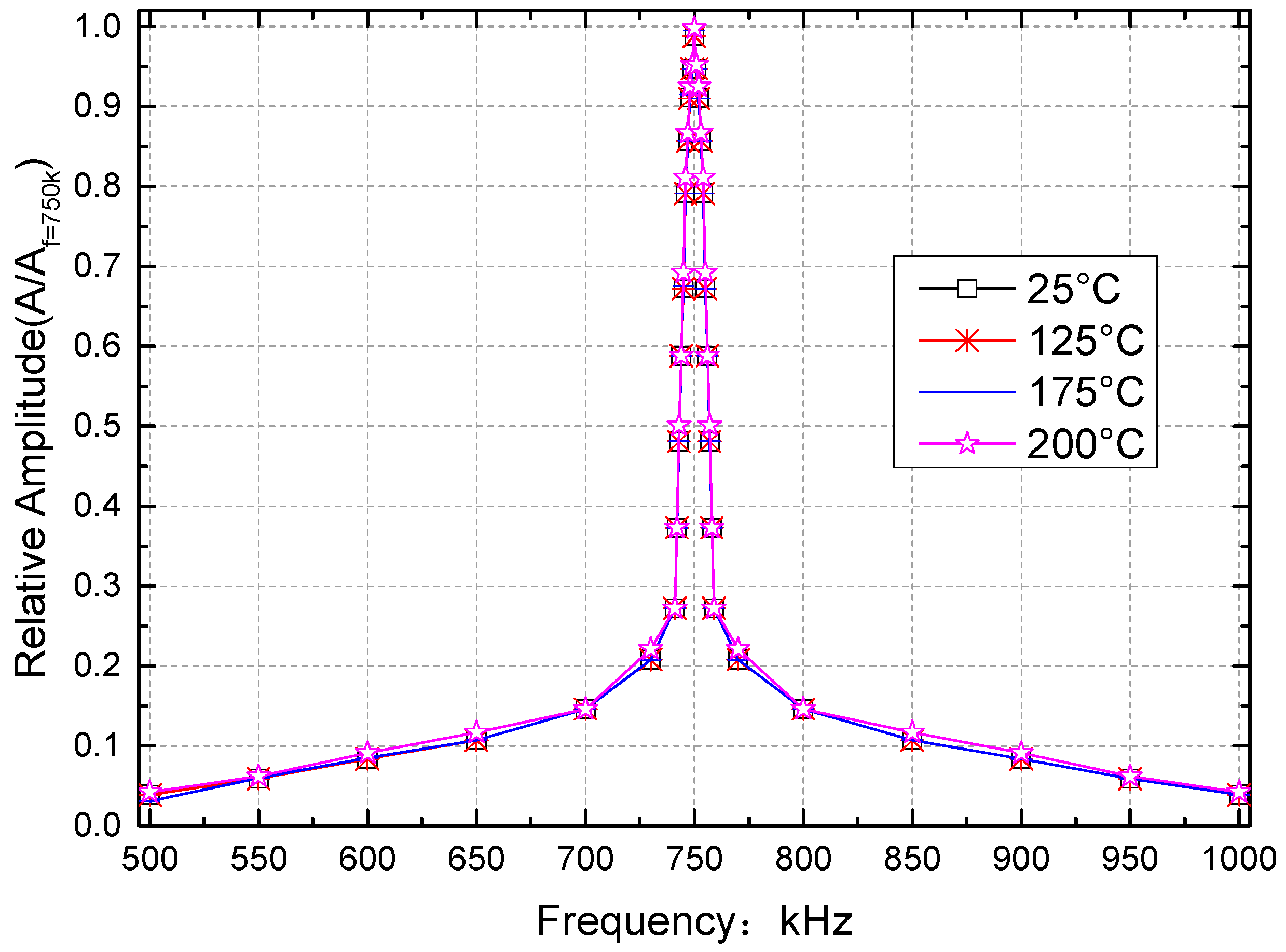
4.2. Q Value
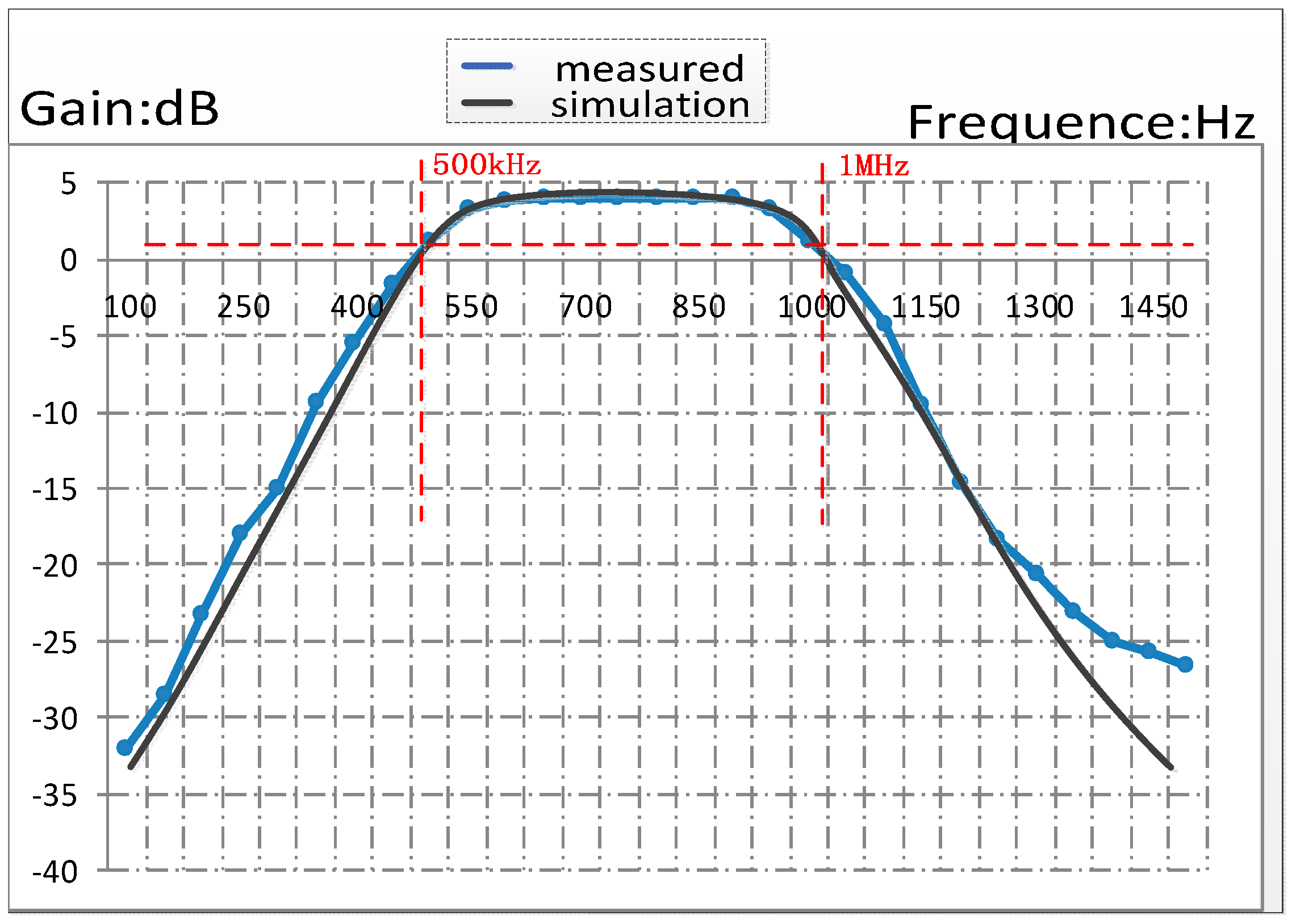
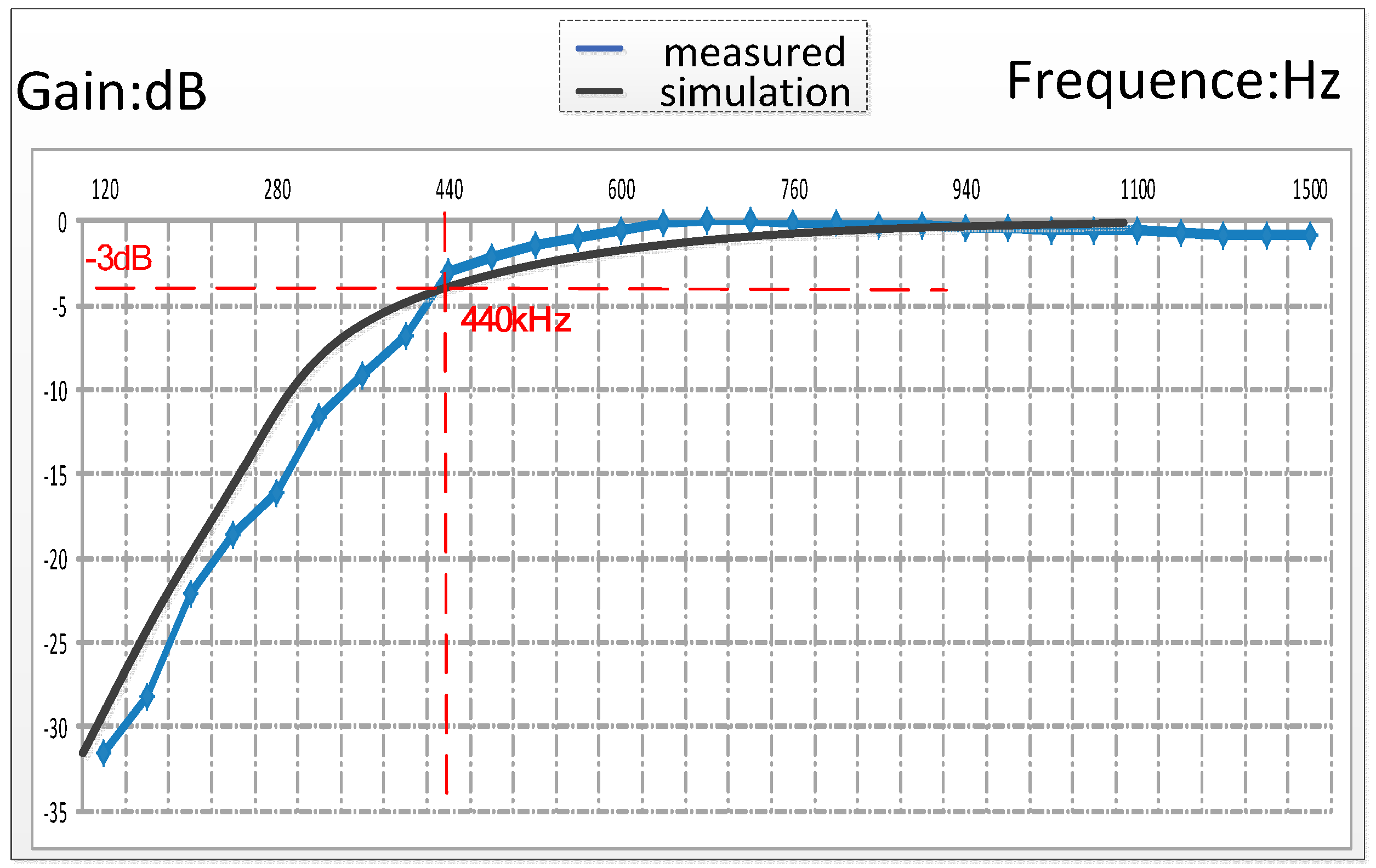
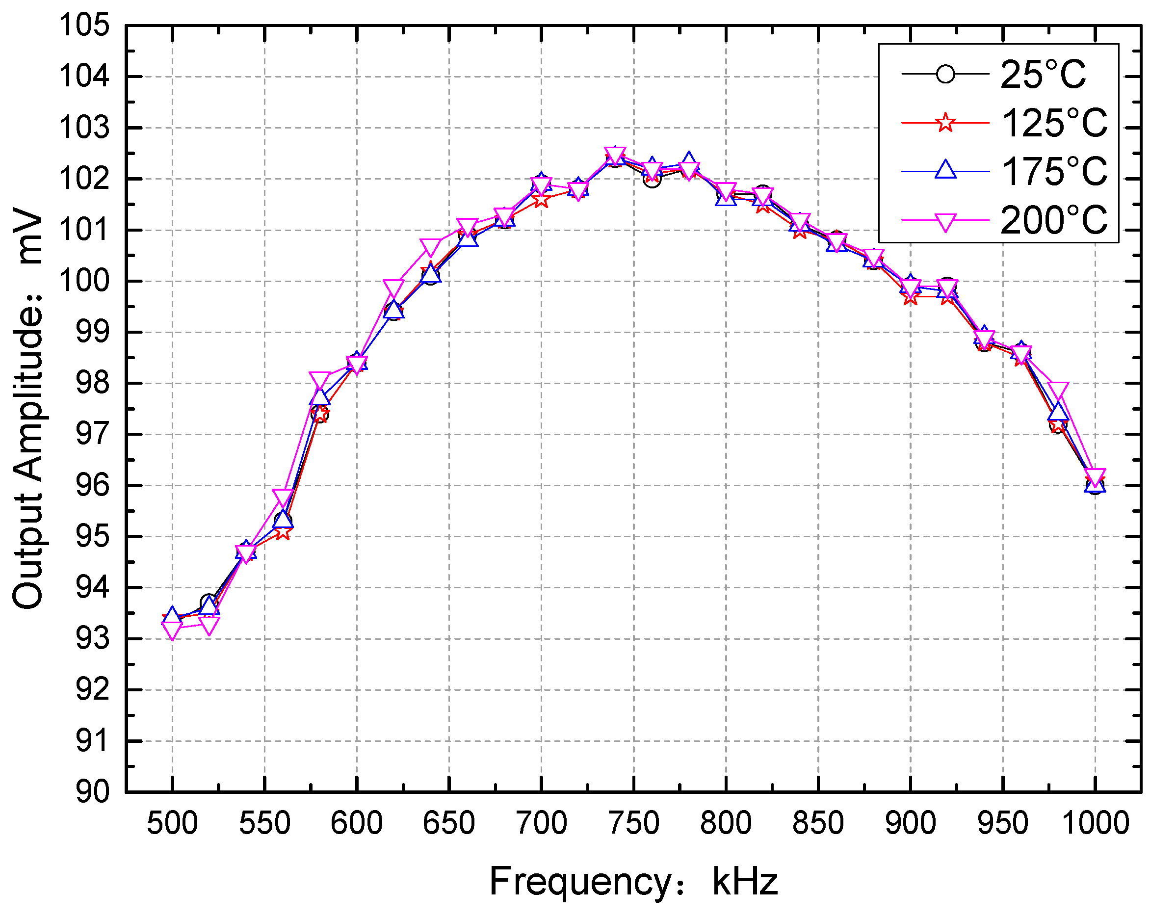
4.3. Frequency Band Characteristic
5. Conclusions
Acknowledgments
Author Contributions
Conflicts of Interest
References
- Garcíaromeo, D.; Valero, M.R.; Medrano, N.; Calvo, B.; Celma, S. A high performance LIA-based interface for battery powered sensing devices. Sensors 2015, 15, 25260–25276. [Google Scholar] [CrossRef] [PubMed]
- Sonnaillon, M.O.; Bonetto, F.J. A low-cost, high-performance, digital signal processor-based lock-in amplifier capable of measuring multiple frequency sweeps simultaneously. Rev. Sci. Instrum. 2005, 76, 024703. [Google Scholar] [CrossRef]
- Díaz-Michelena, M.; Cobos, P.; Aroca, C. Lock-in amplifiers for AMR sensors. Sens. Actuators A Phys. 2015, 222, 149–159. [Google Scholar] [CrossRef]
- Farnham, J.M. A simple low-cost lock-in amplifier for the laboratory. J. Chem. Educ. 2005, 82, 1399–1401. [Google Scholar]
- Clark, B. Method and Apparatus for Optimizing Magnetic Signals and Detecting Casing and Resistivity. U.S. Patent US7962287 B2, 14 June 2011. [Google Scholar]
- Freedman, R.; Anand, V.; Grant, B.; Ganesan, K.; Tabrizi, P.; Torres, R.; Catina, D.; Ryan, D.; Borman, C.; Krueckl, C. A compact high-performance low-field NMR apparatus for measurements on fluids at very high pressures and temperatures. Rev. Sci. Instrum. 2014, 85, 025102. [Google Scholar] [CrossRef] [PubMed]
- Difoggio, R. Method and Apparatus for Reservoir Characterization Using Photoacoustic Spectroscopy. U.S. Patent 7,520,158 B2, 21 April 2009. [Google Scholar]
- Chen, M.Y.; Raghuraman, B.; Bryant, I.; Supp, M.G.; Navarro, J. While-Drilling Apparatus for Measuring Streaming Potentials and Determining Earth Formation Characteristics. U.S. Patent 7,233,150 B2, 19 June 2007. [Google Scholar]
- Avant, C.; Daungkaew, S.; Behera, B.K.; Danpanich, S.; Laprabang, W.; Santo, I.D.; Heath, G.; Osman, K.; Khan, Z.A.; Russell, J. Testing the limits in extreme well conditions. Oilfield Rev. 2012, 24, 4–19. [Google Scholar]
- Dziedzic, A.; Nowak, D. Thick-film and LTCC passive components for high-temperature electronics. Radioengineering 2013, 22, 218–226. [Google Scholar]
- Johnson, R.W.; Evans, J.L.; Jacobsen, P.; Thompson, J.R.; Christopher, M. The changing automotive environment: High-temperature electronics. IEEE Trans. Electron. Packag. Manuf. 2004, 27, 164–176. [Google Scholar] [CrossRef]
- Parrott, R.A.; Song, H.; Chen, K.C. Cooling System for Downhole Tools. U.S. Patent 6,336,408 B1, 8 January 2002. [Google Scholar]
- Rafie, S. Thermal Isolation Devices and Methods for Heat Sensitive Downhole Components. U.S. Patent 7,440,283 B1, 21 October 2008. [Google Scholar]
- Prammer, M.G.; Drack, E.; Goodman, G.; Masak, P.; Menger, S.; Morys, M.; Zannoni, S.; Suddarth, B.; Dudley, J. The magnetic-resonance while-drilling tool: Theory and operation. SPE Reserv. Eval. Eng. 2000, 4, 270–275. [Google Scholar] [CrossRef]
- Chien, C.W.; Lee, S.L.; Lin, J.C.; Jahn, M.T. Effects of Si p size and volume fraction on properties of Al/Si p composites. Mater. Lett. 2002, 52, 334–341. [Google Scholar] [CrossRef]
- Sipio, E.D.; Galgaro, A.; Destro, E.; Teza, G.; Chiesa, S.; Manzella, A.; Giaretta, A. Subsurface thermal conductivity assessment in Calabria (Southern Italy): A regional case study. Environ. Earth Sci. 2014, 72, 1383–1401. [Google Scholar] [CrossRef]
- Jing, W.; Cheng, X. Generalized thermal resistance and its application to thermal radiation based on entransy theory. Int. J. Heat Mass Transf. 2013, 58, 374–381. [Google Scholar]
- Leis, J.; Martin, P.; Buttsworth, D. Simplified digital lock-in amplifier algorithm. Electron. Lett. 2012, 48, 259–261. [Google Scholar] [CrossRef]
- Casanova, F.; Perlo, J.; Blümich, B. Single-Sided NMR; Springer: Berlin/Heidelberg, Germany, 2011. [Google Scholar]
- Li, G.; Zhou, M.; Li, X.X.; Lin, L. Digital lock-in algorithm and parameter settings in multi-channel sensor signal detection. Measurement 2013, 46, 2519–2524. [Google Scholar] [CrossRef]
- Communication, S. Digital Signal Processing with Field Programmable Gate Arrays; Springer: Berlin/Heidelberg, Germany, 2001; pp. 1037–1041. [Google Scholar]
- Umezawa, K.; Branch, J.; Yamagami, H.; Ofuchi, H.; Ohta, B.; Uchida, Y.; Kitahara, H. Department of defense test method standard for environmental engineering considerations and laboratory tests. Ann. Emerg. Med. 2000, 54, S80–S81. [Google Scholar] [CrossRef]
- Azzolini, C.; Magnanini, A.; Tonelli, M.; Chiorboli, G.; Morandi, C. A CMOS vector lock-in amplifier for sensor applications. Microelectron. J. 2010, 41, 449–457. [Google Scholar] [CrossRef]
- Alonso, R.; Villuendas, F.; Borja, J.; Barragán, L.A.; Salinas, I. Low-cost, digital lock-in module with external reference for coating glass transmission/reflection spectrophotometer. Meas. Sci. Technol. 2003, 14, 551–557. [Google Scholar] [CrossRef]


| Name | Material | Thermal Conductivity W/(mm·°C) |
|---|---|---|
| Substrate | PWB | 0.013 |
| Shell | Steel | 0.012 |
| Wafer | Si | 0.161 |
| Gas | Nitrogen | 0.0228 |
| Linkage | Eutectic | 0.295 |
| Bonder | Epoxy | 0.002 |
| Header | Kovar | 0.017 |
| Single Chip | SiP | |
|---|---|---|
| Name | Thermal Resistance (°C/W) | Equivalent Thermal Resistance (°C/W) |
| FPGA | 26.1 | 2.222 |
| MCU | 35.0 | 3.472 |
| ADC | 100.0 | 24.691 |
| DDS | 87.0 | 23.641 |
| SRAM | 76.4 | 4.535 |
| sin_LUT① | sin_LUT② | sin_LUT③ | sin_LUT④ | ||||
| Input | Output | Input | Output | Input | Output | Input | Output |
| 00 | 0 | 00 | 0 | 00 | 0 | 00 | 0 |
| 01 | 0 | 01 | 256 | 01 | 0 | 01 | 7936 |
| 10 | 181 | 10 | 181 | 10 | 8011 | 10 | 8011 |
| 11 | 181 | 11 | 437 | 11 | 8011 | 11 | 7755 |
| cos_LUT⑤ | cos_LUT⑥ | cos_LUT⑦ | cos_LUT⑧ | ||||
| Input | Output | Input | Output | Input | Output | Input | Output |
| 00 | 0 | 00 | 0 | 00 | 0 | 00 | 0 |
| 01 | 256 | 01 | 0 | 01 | 7936 | 01 | 0 |
| 10 | 181 | 10 | 8011 | 10 | 8011 | 10 | 181 |
| 11 | 437 | 11 | 8011 | 11 | 7755 | 11 | 181 |
| Implementation | Occupied Core Cells | Percentage (%) |
|---|---|---|
| Traditional way | 10,076/24,576 | 41% |
| Method of LUT | 3191/24,576 | 13% |
| Parameter | Temperature: T (°C) | |||
|---|---|---|---|---|
| 25 | 125 | 175 | 200 | |
| ε | 1.488% | 1.488% | 1.653% | 1.736% |
| Equivalent Gain (dB) | 96.210 | 96.210 | 96.187 | 96.311 |
| Parameter | Temperature: T (°C) | |||
|---|---|---|---|---|
| 25 | 125 | 175 | 200 | |
| Q | 1042 | 1042 | 1042 | 1041 |
| Parameter | Temperature: T (°C) | ||
|---|---|---|---|
| 125 | 175 | 200 | |
| E’ | −0.00050 | −0.00050 | 0.0010 |
| −0.0011 | 0.0039 | 0.0037 | |
© 2016 by the authors; licensee MDPI, Basel, Switzerland. This article is an open access article distributed under the terms and conditions of the Creative Commons Attribution (CC-BY) license (http://creativecommons.org/licenses/by/4.0/).
Share and Cite
Cheng, J.; Xu, Y.; Wu, L.; Wang, G. A Digital Lock-In Amplifier for Use at Temperatures of up to 200 °C. Sensors 2016, 16, 1899. https://doi.org/10.3390/s16111899
Cheng J, Xu Y, Wu L, Wang G. A Digital Lock-In Amplifier for Use at Temperatures of up to 200 °C. Sensors. 2016; 16(11):1899. https://doi.org/10.3390/s16111899
Chicago/Turabian StyleCheng, Jingjing, Yingjun Xu, Lei Wu, and Guangwei Wang. 2016. "A Digital Lock-In Amplifier for Use at Temperatures of up to 200 °C" Sensors 16, no. 11: 1899. https://doi.org/10.3390/s16111899