Sensing Properties of Multiwalled Carbon Nanotubes Grown in MW Plasma Torch: Electronic and Electrochemical Behavior, Gas Sensing, Field Emission, IR Absorption


 and
and 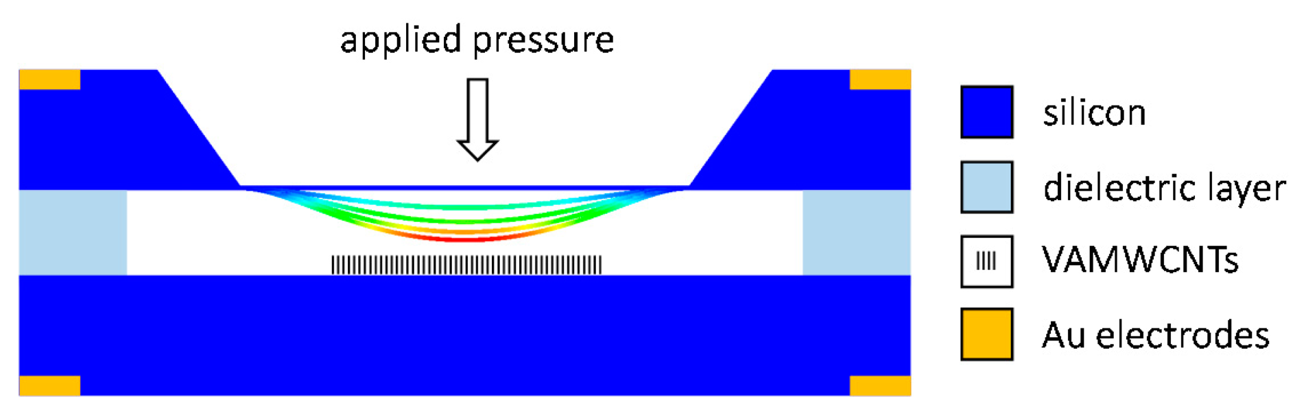
Abstract
: Vertically aligned multi-walled carbon nanotubes (VA-MWCNTs) with an average diameter below 80 nm and a thickness of the uniform VA-MWCNT layer of about 16 μm were grown in microwave plasma torch and tested for selected functional properties. IR absorption important for a construction of bolometers was studied by Fourier transform infrared spectroscopy. Basic electrochemical characterization was performed by cyclic voltammetry. Comparing the obtained results with the standard or MWCNT‐modified screen-printed electrodes, the prepared VA-MWCNT electrodes indicated their high potential for the construction of electrochemical sensors. Resistive CNT gas sensor revealed a good sensitivity to ammonia taking into account room temperature operation. Field emission detected from CNTs was suitable for the pressure sensing application based on the measurement of emission current in the diode structure with bending diaphragm. The advantages of microwave plasma torch growth of CNTs, i.e., fast processing and versatility of the process, can be therefore fully exploited for the integration of surface-bound grown CNTs into various sensing structures.1. Introduction
Carbon nanotubes (CNTs), a synthetic carbon allotrope, are made of sp2 hybridized carbon atoms. Single-walled CNT (SWCNT) is a graphene sheet rolled-up into a seamless cylinder and multi-walled CNT (MWCNT) is composed of several such cylinders, nested concentrically [1,2]. CNTs are often synthesized by a chemical vapor deposition (CVD) in the presence of a catalyst, nanoparticles of transition metals. In thermal CVD, a carbon-containing gas mixture is heated typically to 550–1100 °C by a conventional heat source. Plasma enhanced CVD (PECVD) activates the gas mixture by ignition of plasma discharge but a separate heating of the substrate might be required too [3]. General arguments for the PECVD include low-temperature, easily achieved vertical alignment and large area processing [4].The CVD methods are used for a CNT volume-synthesis and a surface-bound growth of vertically aligned and micropatterned CNT arrays [5]. The vertically-aligned CNTs (VA-CNTs) are highly desirable for the integration into functional devices. The aligned growth can produce CNTs free from amorphous carbon with a very narrow range of tube lengths and diameters, which is an additional advantage for many applications [6].
Unique physical and electrical properties of CNTs, i.e., high electrical conductivity, remarkable mechanical strength, and thermal and chemical stability, predestinate them for many nanotechnology-based applications in electronic, optical and biomedical devices, sensors and composites [7,8]. The application potential of CNTs depends on their properties that are given by their structure and the form in which they are applied. Separated MWCNTs exhibited a non-linearity in I-V characteristics that were relatively large in case of the contacts made by underlying gold electrodes but almost diminished if the contacts were placed on the top of partially etched nanotubes [9]. Theoretically predicted impedance of SWCNT bundles at high frequencies is quite complex, employing resistance R, inductance L and capacitance C, and their validation proved to be difficult [10]. The experimentally proposed circuit model of SWCNTs contains a parallel RC element resulting from the contacts in series with R and L representing the SWCNT intrinsic behavior [10,11]. Similarly, an equivalent circuit model consisting of RC networks is constructed to simulate the electrical responses of MWCNT/polymer composites [12,13].
The optical properties of CNTs help to understand their structure [14], evaluate their purity [15] and open new applications for optical sensing [16,17]. MWCNT-based infrared detectors have received much attention due to MWCNT band gap of 0.4–6.0 eV and high absorption efficiency in IR [18]. A bolometer based on CNT/polymer composites was constructed for the detection of infrared radiation from the range 0.2–20 μm [19] and it was shown that the sensitivity and response time of the CNT-based bolometers can be substantially improved by an appropriate functionalization and selection of organic matrix [19,20].
CNTs exhibit also a great potential for electrochemical sensing due to their unique electrical properties, high surface area, fast heterogeneous electron transfer, and electrochemical stability [21–25]. The CNTs implemented as a VA-CNT film provide other advantages such as a controlled growth in defined areas and an easy modification of their surface demanded for particular sensing or biosensing applications [6]. The as-prepared VA-CNT-based sensors have been successfully applied to detect rutin [26] and salbutamol [27], a prohibited drug in sports. The VA-CNT thin films have also been tested as candidate platforms for DNA immobilization and detection of DNA hybridization [28]. The VA-CNT electrode modified by gold nanoparticles has been used for non-enzymatic detection of uric acid [29] and a platinum nanoparticle-modified VA-CNT electrode for detection of L-cysteine [30].
The CNTs belong to a group of new materials that have been extensively tested for gas sensing during the last 10 years and much effort has been put into the development of gas sensors working at room temperature. In spite of many papers devoted to SWCNT-based gas sensors [31–33], the MWCNTs can be also successfully used [34–36] and are preferable because of their low costs. The construction of room temperature ammonia (NH3) sensors is an important task because NH3 is a dangerous gas having a negative influence on the environment and humans. Cui et al. created a sensor with MWCNTs decorated by Ag nanocrystals that exhibited an enhanced response of 9% to 10,000 ppm of NH3 as well as fast recovery [37]. A high sensitivity—6.2% to 4000 ppm of NH3—was proven for Co1−xNixFe2O4/MWCNT composites [38]. Varghese et al. investigated sensitivity of resistive and capacitive MWCNT sensors for different gases such as water vapors, NH3, CO2 and CO [39].
CNTs have been also considered as promising field emitters due to their low turn-on filed, long emitter lifetime and good emission stability [40]. The field-emitter configuration should have the highest aspect ratio and low work function at its surface. The first extensive study of field emission from CNTs has been published by Bonard et al. in 1998 [41]. Later on, CNTs were used as field-emitters in flat-panel field-emission displays [42] or electron sources in electron microscopes [43].
In the present work, a promising application potential of VA-MWCNTs grown by PECVD in microwave (MW) plasma torch [44,45] is explored in detail. Previous studies of the CNTs deposited by the MW plasma torch revealed possible improvements of the process [46] and provided a basic structural characterization of the CNTs using scanning and transmission electron microscopies and Raman spectroscopy [47]. The technology based on the MW torch is a high speed process that takes only 60–120 s including catalyst activation (restructuralization of a catalytic thin film into nanoparticles) and does not require any external heating source of the substrate. Besides starting the CNT growth with a thin catalytic film deposited on the substrate in a separate technological step, it offers the possibility to prepare catalytic nanoparticles during the same process, i.e., using the MW plasma torch [48]. Another advantage is a successful preparation of vertically aligned MWCNTs directly on Si without using a barrier SiO2 layer [3]. A direct contact between the VA-CNTs and the Si substrate can be very important for some applications and it enables the construction of a field-emission based pressure sensor [49]. Besides the field emission, other functional properties (electrical and electrochemical, gas sensing, IR absorption) of the CNTs from the MW plasma torch are tested. Thus, the present work investigates and summarizes the CNT properties directly related to particular sensing applications and in some cases (field-emission pressure sensor, electrochemical sensor, gas sensor) describes the sensor structure and its preparation.
2. Experimental Section
2.1. CNT Deposition and Structural Characterization
The VA-MWCNT layers were deposited from Ar/CH4/H2 mixtures using the atmospheric pressure MW plasma torch operated at the power of 210 W. The flow rates of Ar, CH4 and H2 were QAr = 700 sccm, QCH4 = 19–38 sccm and QH2 = 250 sccm, respectively. The substrate for the CNT growth was heated by the interaction with plasma, and its temperature (950–1050 K) was regulated by the distance from the plasma torch nozzle. The CNT growth time, that included also the catalyst activation phase, varied from 60 to120 s.
The aim of the present work was to investigate functional properties of the CNTs deposited by MW torch and, in some cases, integrate them into sensing devices. Most of the measurement structures were based on Si due to its compatibility with microelectronic chips and microelectromechanical systems (MEMS). CNTs were grown either on a polished single crystal silicon (c-Si) substrate, the c-Si coated with an adhesive metallic interlayer or the c-Si coated with in a thermal silicon oxide (SiO2) film. The latter is used if the application requires a dielectric or thermal separation of the CNTs. The thickness of SiO2 film did not play a significant role and was chosen arbitrarily. The substrate details are given in the following sections describing each particular measurement structure.
A vacuum evaporated Fe film, 5 nm in thickness, or Fe nanoparticles (NPs) deposited on the substrate by MW torch from iron pentacarbonyl (Fe(CO)5) vapors were used as catalysts. The details of the NPs deposition are described in previous papers [50,51]. The Ar flow through the central torch nozzle and through the blower with liquid Fe(CO)5 were 700 and 28 sccm, respectively. The Ar flow of 28 sccm through the blower with the liquid corresponds to 0.1 sccm of Fe(CO)5. The deposition time was 10 s.
Surfaces and cross sections of the prepared CNT samples were checked by the Tescan MIRA II LMU scanning electron microscope (SEM, TESCAN, Brno, Czech Republic) using 15 kV acceleration voltage.
2.2. Characterization of Electrical Behavior of CNTs
The CNTs for electrical characterization, such as I-V characteristics and sheet resistance measurements, were grown in the MW plasma torch on p-type, boron-doped, c-Si substrates (8 mm × 8 mm, thickness 525 μm, resistivity <6 Ω·cm−1) coated by the SiO2 film, 300 nm in thickness, and the top Fe catalytic layer. The square chips fully covered with CNT films were finished by vacuum evaporation of gold pads (0.5 mm × 0.5 mm) in each sample corner.
The chips were investigated at the probe station Cascade M150 connected to the Keithley SCS-4200 semiconductor analyzer (Keithley Instruments, Inc., Cleveland, OH, USA). The I-V characteristics of the films were measured between the opposite corners in the voltage range from −5 V to +5 V. The specific electrical resistance was determined by Van der Pauw measurement which was carried out automatically by the Keithley SCS-4200 analyzer.
For the impedance spectroscopy, the CNTs were grown on a SITAL glass-ceramic substrate (10 mm × 15 mm, thickness 525 μm) using Fe catalytic layer. This substrate was chosen to suppress the effect of Si substrate properties during the impedance spectroscopy measurement. The VA-MWCNTs were deposited on a central circular area, 6 mm in diameter. Two circular gold contacts of 3 mm in diameter were prepared by vacuum evaporation. The impedance was measured using the Agilent E4980A Precision LCR meter (Agilent Technologies, Santa Clara, CA, USA) and data acquisition by LabView software (National Instruments, Austin, TX, USA). The measurements were performed in the frequency range from 20 Hz to 2 MHz with the voltage level of 0.5 V.
2.3. IR Absorption
The FTIR measurement procedure is a simple way to compare samples with or without grown CNTs in order to consider CNTs as possible IR detector. The CNTs for infrared absorption measurements were grown on the same substrates as described in the previous Section 2.2, i.e., c-Si substrate with the SiO2/Fe double layer. In the case of the bolometer, thin SiO2 layer is needed for construction of low thickness MEMS diaphragm to suppress thermal loses to the substrate mass [52].
The IR absorption of VA-CNTs on the Si substrate covered by 300 nm thick SiO2 film was investigated with the Fourier transform infrared (FTIR) spectrometer Nicolet iS50 in the attenuated total reflection (ATR) mode. The ATR crystal was pressed against the sample and the measurement was performed in the wavelength range 2.5–22.5 μm. The absorbance of the VA-CNT sample was compared to the absorbance of Si substrate covered by 300 nm thick SiO2 film and 5 nm thick Fe film used as catalyst of the CNT growth.
2.4. Electrochemical Characterization
The preparation of samples for the electrochemical measurements started with n-type, highly antimony-doped, c-Si substrates (5 mm × 30 mm, thickness 525 μm, resistivity <0.02 Ω·cm−1) coated by the SiO2 film, 300 nm in thickness. The working electrode had dimensions 4.5 mm × 4.5 mm and consisted of the CNTs deposited in the MW plasma torch (Section 2.1). Before the CNT growth, the SiO2 insulating film was removed from the working electrode area by a wet chemical etching in buffered HF and the area of the working electrode was covered by magnetron sputtered Ti (10 nm)/Ta (250 nm) double layer and vacuum evaporated top Fe film, the catalyst for the CNT growth. The Ti/Ta coating was necessary to ensure a good adhesion of the CNTs that otherwise peeled off the substrate when immersed in an electrolyte. The highly doped Si substrate was needed for a good electrical connection between the CNT layer and the contact pads which were situated on the opposite end of the substrate with the same dimensions as the electrode.
Electrochemical response of the [Fe(CN)6]4−/3− redox couple mediated by the CNT electrode was investigated by the cyclic voltammetry (CV) with AUTOLAB PGSTAT 204 potentiostat/galvanostat controlled by Nova 1.10 software (Metrohm Autolab B.V., Utrecht, The Netherlands). A standard three-electrode voltammetric cell employing an Ag/AgCl reference electrode (type 6.0729.100, Metrohm, Herisau, Switzerland) and a platinum auxiliary electrode (type 6.0343.000, Metrohm) was used for all the experiments. The electrolyte was an equimolar solution of 2.5 mM potassium ferrocyanide and potassium ferricyanide ([Fe(CN)6]4−/3−) in 0.1 M KCl. The cyclic voltammograms were recorded in the potential range from −1 V to +1 V with scan rates (υ) from 5 to500 mV·s−1.
2.5. Gas Sensing Properties
The CNTs for testing the gas sensing properties were prepared on the p-type, boron-doped, c-Si substrates (8 mm × 8 mm, thickness 525 μm, resistivity <6 Ω·cm−1) coated with the 92 nm thick SiO2 film. The catalytic Fe nanoparticles were deposited by the MW plasma torch (see Section 2.1) in the central area, 4 mm × 4 mm, of the substrate. This form of the Fe catalyst was chosen for the growth of a less dense CNT mesh because the gas sensing application requires a large surface area and dense CNTs mask each other. The CNTs were grown from Fe NPs in the MW plasma torch (Ar = 700 sccm, H2 = 250 sccm, CH4 = 38 sccm, deposition time 60 s, deposition temperature 973 K) as described in Section 2.1. The measurement chip was finished by vacuum evaporated gold contacts (15 nm NiCr adhesion layer with 350 nm Au layer on the top) with a size of 2 mm × 6 mm centered symmetrically to the middle of the sensor.
The gas sensing properties were determined as a change of the sample resistance during its exposure to a gaseous analyte, either ammonia (NH3) or isobutane (iC4H10). The measurements were performed in a custom-built gas station equipped with two gas channels and one chamber for two sensors' characterization at once. One gas channel is used for the synthetic air as a carrier gas. The second gas channel supplies diluted analytes, NH3 or iC4H10 in nitrogen. The response of the sensors was determined at different analyte concentrations, namely 100 ppm, 250 ppm and 500 ppm. Before each measurement, a sample conditioning was carried out for 30 min at 200 °C in the air flow of 1000 sccm. The sensor response was defined as
2.6. Field Emission Properties for Pressure Sensing
The MEMS field emission pressure sensor was designed as a diode structure (see Figure 1). It consisted of two n-type, highly antimony-doped, c-Si electrodes (10 mm × 15 mm, thickness 525 μm, resistivity <0.02 Ω·cm−1). One of them was anisotropically etched to a bending diaphragm. The other was coated by an emissive material, the VA-MWCNTs deposited in the MW plasma torch (see Section 2.1). The highly doped Si substrate was needed for a good electrical connection between the CNT layer and the contact pads. The Fe catalytic film, required for the growth of CNTs, was deposited in the center of the substrate on the area of 4 mm × 4 mm. A native oxide film on Si was removed by HF prior to the deposition of the Fe film, thus ensuring the electrical contact between CNTs and Si. The field-emission pressure sensor is proposed to be constructed by the separation of the electrodes with a dielectric layer creating an integrated evacuated volume. The dielectric layer can be made of Pyrex or Simax glass using anodic bonding technology or made of glass frit using a screen printing process.
The measurements of the field emission properties were carried out in a vacuum chamber at pressure lower than 10−4 Pa. A diaphragm bending was simulated by the linear nano-motion drive SmarAct enabling precise changes of the distance between the two electrodes inside the vacuum chamber with the step from 50 nm to1000 nm. The initial distance of 120 μm was established using a solid dielectric foil that was then removed and the emitter-to-anode distance was set up with the SmarAct drive from 84 μm to120 μm. The measurement voltage from 0 to150 V was automatically applied using software communicating via GPIB with the voltage supply.
3. Results and Discussion
3.1. SEM of CNTs
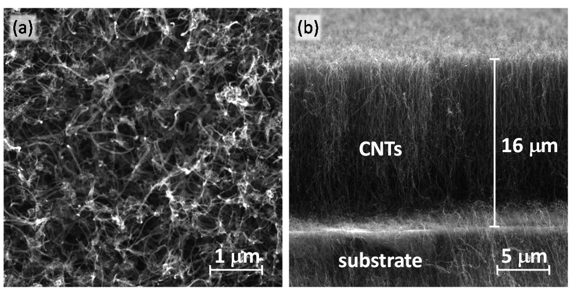
A fast growth of VA-MWCNT films on the c-Si and c-Si/SiO2 substrates has been achieved in MW plasma torch operated at atmospheric pressure without an external heating source [44,45]. The characterization of the VA-MWCNT films by SEM, transmission electron microscopy (TEM), Raman spectroscopy and the influence of process parameters on the CNT growth were discussed in detail in our previous publications [3,46,47]. Typical SEM images of prepared VA-MWCNT film are shown in Figure 2. Although the cross-sectional view in Figure 2b confirms the vertical alignment of the CNT film, the top view (Figure 2a) reveals that the alignment at the end of nanotubes is not perfect. The CNTs having a high aspect ratio, less than 80 nm in the diameter and a length of about 16 μm, are curled at the top end due to different heights. Therefore, top view micrographs cannot provide sufficient information about the structure of all the CNT film.
3.2. Electrical Properties of CNTs
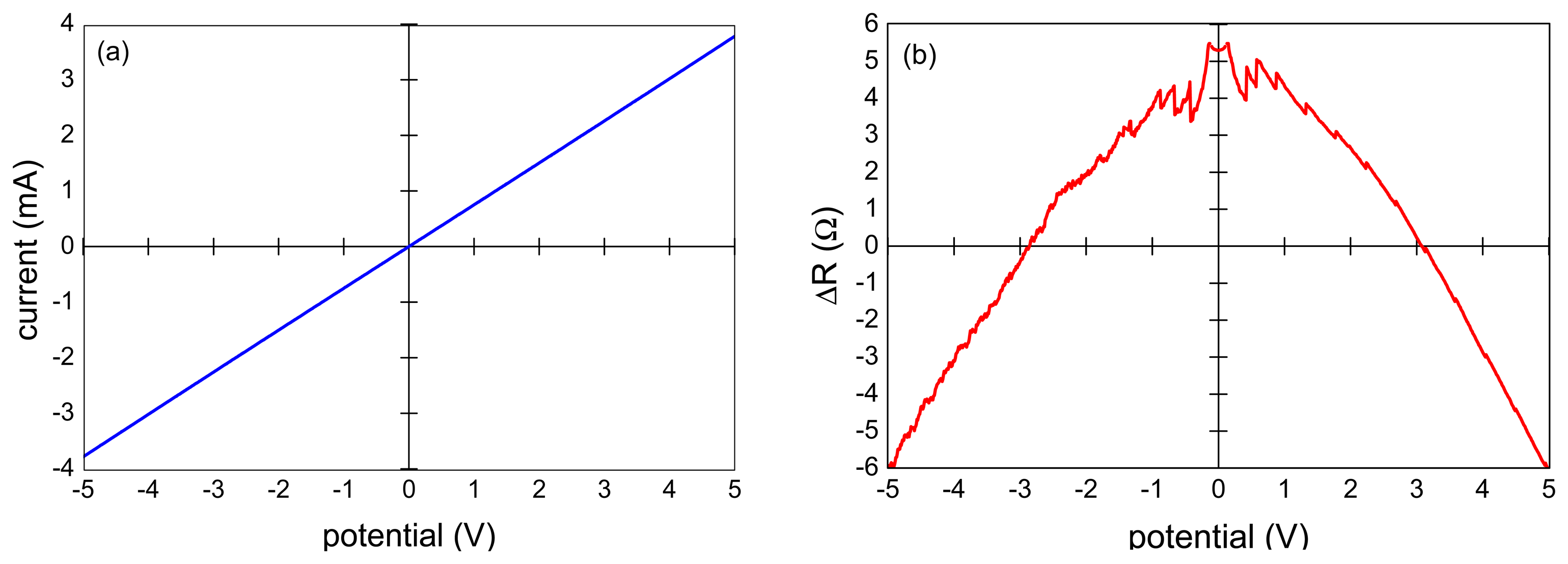
The measured I-V characteristics of the VA-MWCNT samples were nearly linear as documented in Figure 3a for the sample shown in Figure 2. The resistance was in the range of 1–1.3 kΩ. The specific electrical resistance was about 0.5 Ω·cm as calculated from Van der Pauw measurement and the film thickness of 16 μm determined by SEM. A small nonlinearity was revealed when the difference of the sample resistance and its linear approximation was plotted (Figure 3b). The deviation from linear behavior was governed by an exponential growth with a small exponent. The nonlinearity of the CNT resistance did not exceed 6 Ω which corresponded to 0.5% of the film resistance.
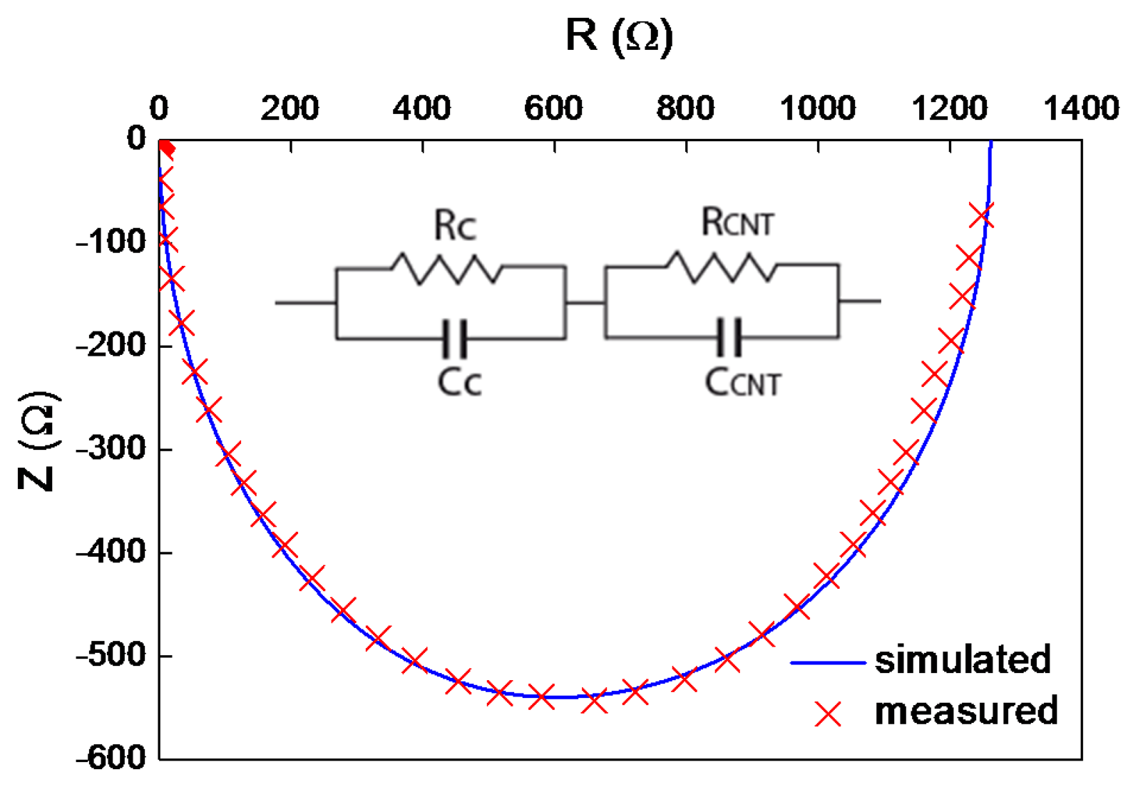
Fitting of the impedance measurements confirmed a simple RC model of two resistances and capacitances in parallel (Figure 4). According to Plombon et al. [10], the contact pads added a significant part of the RC circuit element. The RC/CC circuit represents the contact impedance, and RCNT/CCNT stands for the impedance of the vertically aligned CNT film. The resistances of the contact and the CNT films were 500 and 700 Ω, respectively. The capacitance of the contacts was much higher, about 15 nF, than the capacitance of the CNT film, 3.5 nF. It means that the surface of nanotubes is not pure enough to create a good contact. Adsorbed molecules such as water, CO2 and O2 can create a dielectric film that contributes to its high capacitance.
3.3. IR Absorption
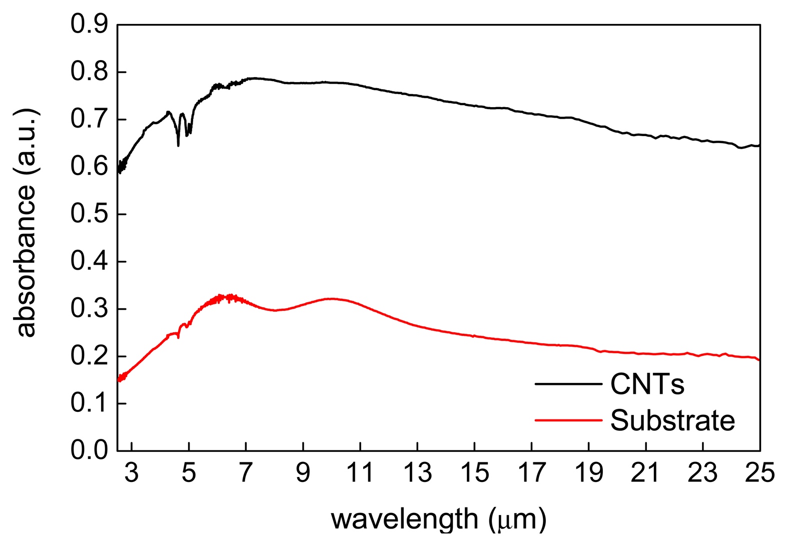
The results of the ATR-FTIR study are shown in Figure 5. They indicate that the VA-MWCNTs can be affectionately applied as a possible absorption layer for IR detection. The mean absorbance value of nearly 80% was obtained. In Figure 5, the interval from 2.5 μm to 7.5 μm represents the absorbance of substrate. The local low points of the curve at approximately 9.0 μm show the typical progression for the atmospheric humidity. The absorbance of the CNTs is mostly seen in the interval from 8 μm to 22 μm which therefore includes the atmospheric window for IR detection.
From the physical principle of the material absorption, it has been well known the particle dipole moment is necessary. No modification is required for CNTs to create the dipole moment according to this measurement. The absorption in the IR region causes changes of vibrational and rotational status of the molecules. The absorption intensity depends on the IR photon energy which can be transferred to the molecule and this depends on the change of the dipole moment that occurs as a result of molecular vibration. As a consequence, a particle will absorb the IR light only if the absorption causes a change in the dipole moment. The absorption frequency is dependent on the vibrational frequency of the molecule.
3.4. Electrochemical Properties
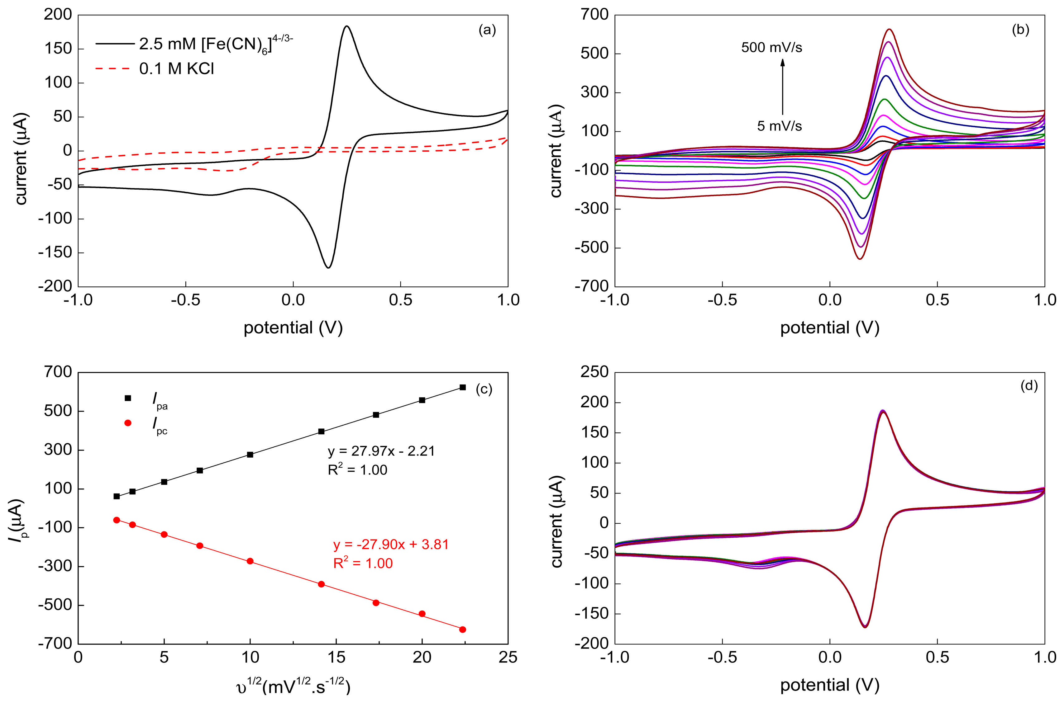
A representative cyclic voltammogram recorded at 50 mV·s−1 with the VA-MWCNT electrode and 2.5 mM [Fe(CN)6]4−/3− (1:1) solution in 0.1 M KCl is shown in Figure 6a. Two well-defined symmetric redox peaks separated by ΔEp = (Epa − Epc) = 83 mV were observed. The ratio of the anodic and cathodic peak currents reached unity (Ipa/Ipc = 1.01). The results indicated that the VA-MWCNT electrode promote electron transfer quite well.
The effect of varying scan rates was studied for the scan rate range 5–500 mV·s−1. The corresponding cyclic voltammograms are given in Figure 6b. The anodic (Ipa) and cathodic (Ipc) peak currents varied linearly with the square root of the scan rate (υ1/2), as shown in Figure 6c. It demonstrates that the electrode process is controlled by a diffusion. The stability of the VA-MWCNT electrode was studied for the [Fe(CN)6]4−/3− in 0.1 M KCl at 50 mV·s−1 using 10 cycles of CV. The results, depicted in Figure 6d, revealed that both, the oxidative and reductive, peak currents of the studied redox couple remained practically constant throughout all 10 potential cycles and, therefore, the CNT-based working electrodes with the Ti/Ta adhesive interlayers are suitable for repeated measurements.
Comparing the obtained results with the standard or MWCNT-modified screen-printed electrodes [53], the prepared VA-MWCNT electrodes indicate their high potential for construction of electrochemical sensors or biosensors detecting substances in aqueous solutions.
3.5. Gas Sensing Properties
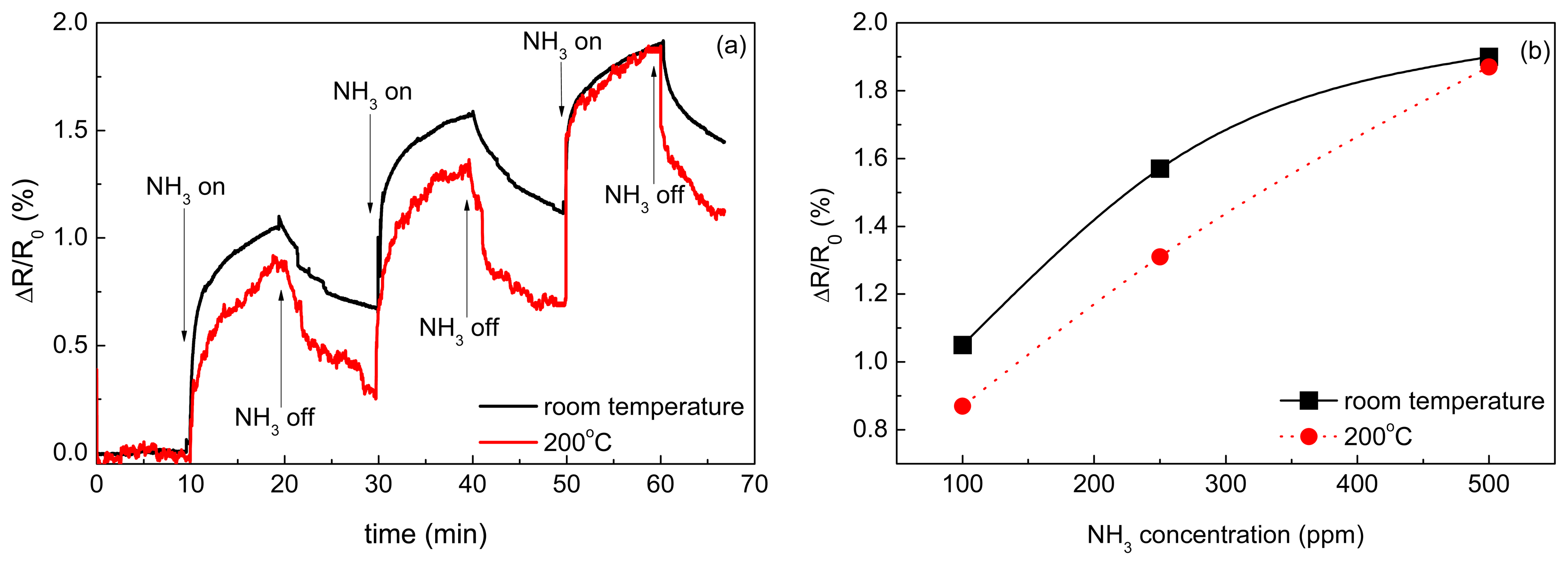
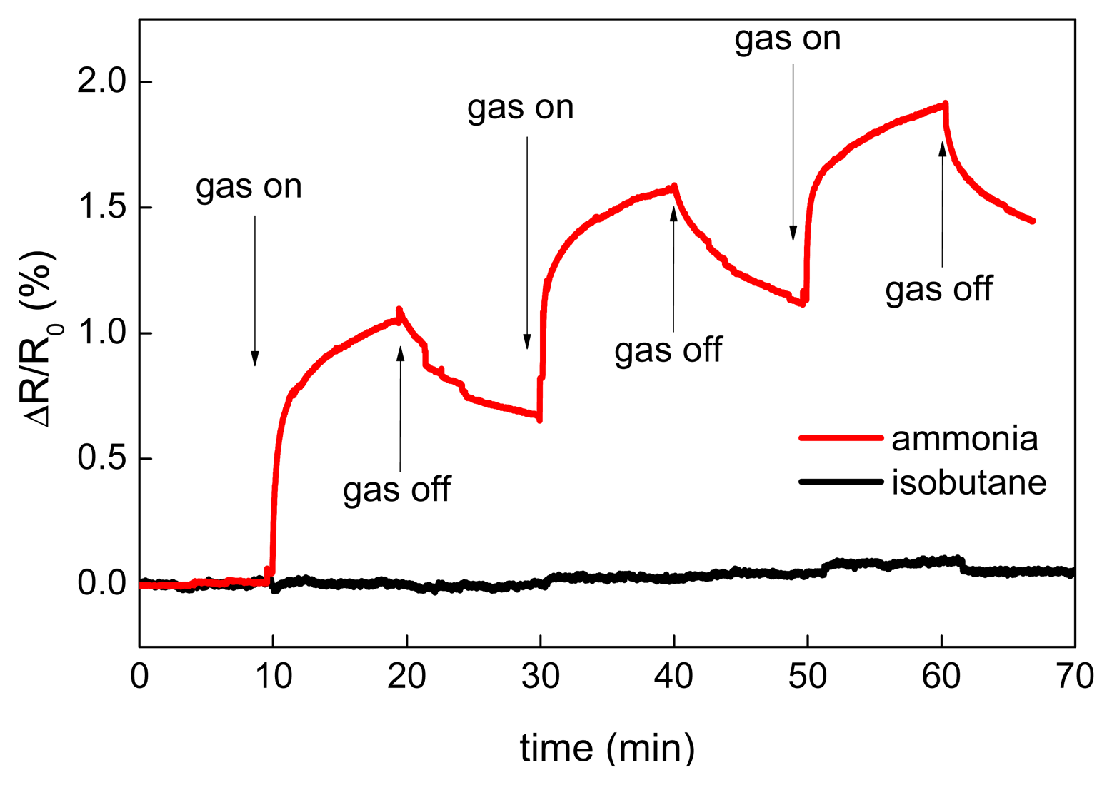
The results of the CNT sensor response to NH3 at room temperatures and 200 °C are shown in Figure 7a. Since the sensor resistance increased during ammonia exposure, it is concluded that free carriers—the holes—in MWCNTs were neutralized by electrons coming from adsorbed NH3 and, therefore, MWCNTs exhibited p-type nature. This phenomenon has been already described in previous studies. Hoa et al. supposed that MWCNT is a p-type semiconductor and the adsorption of electron donor compound such as NH3 decreases the charge carrier concentration, thus inducing an increase of the resistance [54]. The same mechanism of interaction of adsorbed electron-donor compound with p-type CNTs was also described in [34,55–57]. The main interaction mechanism of ammonia with CNTs is a reversible adsorption. Vikramaditya et al. assume that NH3 is physisorbed on non-doped CNTs [58]. Thus, the sensing mechanism of ammonia with CNTs consists of two main steps, (i) physical adsorption of gas molecules and (ii) a charge transfer between adsorbed molecules and CNTs [59,60]. Testing of the sensor sensitivity to isobutane was carried out at room temperature (Figure 8) and revealed that the sensor is insensitive to a non‐polar molecule such as iC4H10.
According to the data presented in Figure 7b, the sensor exhibited higher response to NH3 at the room temperature than at 200 °C. Since the adsorption is an exothermal process, it is enhanced with the decreasing temperature. The response ΔR/R0 ranged from 0.87% to 1.9%. The dependence of the sensor response ΔR/R0 determined after 10 min of the exposure on the concentration of NH3 was almost linear at 200 °C whereas the relation became strongly nonlinear at room temperature. It can be linked to an incomplete desorption of NH3 at room temperature.
The obtained response of the sensors to NH3 was quite high taking into account that MWCNTs were not treated or modified for sensing. The highest response, 1.9%, was achieved at room temperature for 500 ppm of NH3. For comparison, Hoa et al. [54] achieved 8% response for 6% of NH3 in N2, i.e., for 60,000 ppm. Here, the reported sensor was not tested for such a high concentration of NH3 but its response to a 120× lower concentration was only four times lower. A response of 9%, but to a lower concentration of 1% (10,000 ppm), was reported by Cui et al. for Ag-decorated MWCNTs [37].
In conclusion, the described sensor preparation technique is quite simple and allows achieving a sufficiently high response. The direct nanotube growth on the substrate allows managing the response by synthesis conditions that is critical for a scale-up production. The present CNT sensor can be further improved by a suitable functionalization and/or a decoration of the CNTs with metallic nanoparticles using the same set-up or a different procedure.
3.6. Field Emission Properties for Pressure Sensing
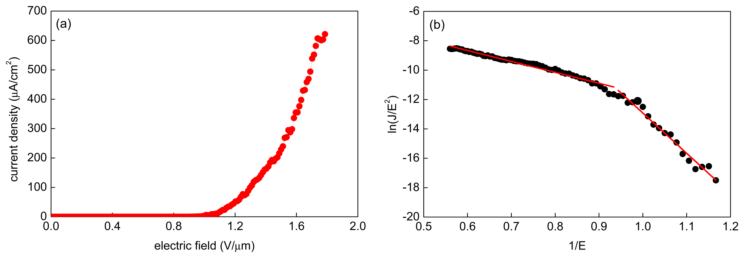
The measurements of field emission current were carried out multiple times at 10 emitter-to-anode distances from 84 μm to120 μm. The current density in dependence on the electric field intensity calculated from measured results is shown in Figure 9a and the corresponding Fowler-Nordheim (F-N) plot is in Figure 9b. Straight lines in the F-N plot indicates the quantum mechanical tunneling characteristic of the electron field emission and are based on the F-N equation
The turn-on field, defined as the field intensity enabling the emission current density of 10 μA·cm−2, was determined to be below 1 V·μm−1. The current density of hundreds of μA was achieved already at 1.8 V·μm−1. The measured data follow the Fowler-Nordheim law in Equation (2) concerning the dependence of the emission current on the electrode distance when the applied voltage is fixed. Similarly, for the fixed distance between the electrodes, the emission current increases with increasing voltage. This confirms the expected behavior of our field emission electrode as proposed in the pressure sensor design. From the measured characteristics, one could also conclude that it is of advantage to operate at a higher electric field and shorter distances. In these conditions, a bigger change of the emission current with changing diaphragm deformation (pressure) leads to the higher sensitivity of the sensor, i.e., higher ΔI/Δp with the identical Δd. This effect can be strengthened with the proper choice of diaphragm [49].
4. Conclusions
Selected functional properties of VA-MWCNT films were investigated in different types of measurement devices that integrated CNTs prepared in a microwave plasma torch. The average diameter of prepared MWCNTs was lower than 80 nm and the thickness of uniform VA-MWCNT layers was about 16 μm. Electrical measurements of CNTs showed their resistive behavior with a low resistance of 0.5 Ω·cm, and non-linearity of about 0.5%. A parallel capacitance proposed in previously published papers was confirmed by dynamic measurements. The FTIR analysis demonstrated a high absorption in the IR range of 8–22 μm allowing VA-MWCNT application in IR thermometers such as bolometers usually used in thermo-vision. Cyclic voltammetry using redox couple of [Fe(CN)6]4−/3− were used to investigate the electrochemical response of the working electrodes coated by plasma grown VA-MWCNTs. The obtained results indicated good electrochemical properties (Ipa/Ipc = 1.01, ΔEp = 83 mV) and confirmed that studied VA-MWCNT working electrodes can be successfully used in the construction of electrochemical sensors.
The constructed resistive sensor based on VA-MWCNTs exhibited increasing resistance of the VA-MWCNT layer when exposed to NH3 that must be explained by the p-type semiconducting behavior of CNTs when adsorbed ammonia gas molecules donate electrons to CNTs. The field emission properties of the electrode with VA-MWCNTs grown directly on silicon were investigated with the aim to use the electrode in pressure sensing applications. The measured dependencies showed that emission current from the CNTs is stable, and a relatively low noise can be achieved for smaller electrode distances and higher voltage between the electrodes. The characteristics were reversible, with low turn-on field (1 V·μm−1), and current of hundreds of μA for the electric field was around 1.8 V·μm−1. It indicated that plasma-grown VA-MWCNTs are well suited for pressure sensing.
Acknowledgments
This work has been performed in laboratories supported by the operational program Research and Development for Innovation, by the SIX project CZ.1.05/2.1.00/03.0072 and supported by Grant Agency of the Czech Republic under the contracts GACR P205/10/1374 and GA13-19947S. Petr Synek would like to acknowledge the project “Employment of Newly Graduated Doctors of Science for Scientific Excellence” (CZ.1.07/2.3.00/30.0009) co-financed from European Social Fund and the state budget of the Czech Republic.
Author Contributions
P.M. and J.P. (Jan Prášek) designed, performed, evaluated and wrote the experiments related to the electrochemical and surface characterization and finalized the paper; J.S. designed and performed the experiments related to the standard electrical characterization which was analyzed, evaluated and written by J.H.; J.P. (Jan Pekárek) designed, performed, evaluated and wrote the experiments related to the field emission properties; V.S. designed, performed, evaluated and wrote the experiments related to the optical characterization; A.G.B. designed, performed, evaluated and wrote the experiments related to the gas sensing properties; O.J., P.S. and M.E. fabricated electrodes and described the fabrication process; L.Z. described the fabrication process and made the final proofs.
Conflicts of Interest
The authors declare no conflict of interest.
References
- Meyyappan, M. Carbon Nanotubes: Science and Applications, 1st ed.; CRC Press: Boca Raton, FL, USA, 2005; p. 304. [Google Scholar]
- Backes, C. Noncovalent Functionalization of Carbon Nanotubes: Fundamental Aspects of Dispersion and Separation in Water; Springer: Berlin, Germany, 2012; p. 203. [Google Scholar]
- Zajíčková, L.; Jašek, O.; Eliáš, M.; Synek, P.; Lazar, L.; Schneeweiss, O.; Hanzlíková, R. Synthesis of carbon nanotubes by plasma-enhanced chemical vapor deposition in an atmospheric-pressure microwave torch. Pure Appl. Chem. 2010, 82, 1259–1272. [Google Scholar]
- Yen, J.H.; Leu, I.C.; Wu, M.T.; Lin, C.C.; Hon, M.H. Density control for carbon nanotube arrays synthesized by ICP-CVD using AAO/Si as a nanotemplate. Electrochem. Solid State Lett. 2004, 7, H29–H31. [Google Scholar]
- Prášek, J.; Drbohlavová, J.; Chomoucká, J.; Hubálek, J.; Jašek, O.; Adam, V.; Kizek, R. Methods for carbon nanotubes synthesis-review. J. Mater. Chem. 2011, 21, 15872–15884. [Google Scholar]
- Chen, H.; Roy, A.; Baek, J.B.; Zhu, L.; Qu, J.; Dai, L.M. Controlled growth and modification of vertically-aligned carbon nanotubes for multifunctional applications. Mater. Sci. Eng. R-Rep. 2010, 70, 63–91. [Google Scholar]
- Tsierkezos, N.G.; Szroeder, P.; Ritter, U. Multi-walled carbon nanotubes as electrode materials for electrochemical studies of organometallic compounds in organic solvent media. Monatshefte Chem.-Chem. Mon. 2011, 142, 233–242. [Google Scholar]
- Tsierkezos, N.G.; Szroeder, P.; Ritter, U. Application of Films Consisting of Carbon Nanoparticles for Electrochemical Detection of Redox Systems in Organic Solvent Media. Fuller. Nanotub. Carbon Nanostruct. 2011, 19, 505–516. [Google Scholar]
- Ahlskog, M.; Hakonen, P.; Paalanen, M.; Roschier, L.; Tarkiainen, R. Multiwalled carbon nanotubes as building blocks in nanoelectronics. J. Low Temp. Phys. 2001, 124, 335–352. [Google Scholar]
- Plombon, J.J.; O'Brien, K.P.; Gstrein, F.; Dubin, V.M.; Jiao, Y. High-frequency electrical properties of individual and bundled carbon nanotubes. Appl. Phys. Lett. 2007, 90. [Google Scholar] [CrossRef]
- Ksenevich, V.K.; Gorbachuk, N.I.; Poklonski, N.A.; Samuilov, V.A.; Kozlov, M.E.; Wieck, A.D. Impedance of Single-Walled Carbon Nanotube Fibers. Fuller. Nanotub. Carbon Nanostruct. 2012, 20, 434–438. [Google Scholar]
- Geng, S.N.; Wang, P.; Ding, T.H. Impedance characteristics and electrical modelling of multi-walled carbon nanotube/silicone rubber composites. Compos. Sci. Technol. 2011, 72, 36–40. [Google Scholar]
- Allaoui, A.; Hoa, S.V.; Pugh, M.D. The electronic transport properties and microstructure of carbon nanofiber/epoxy composites. Compos. Sci. Technol. 2008, 68, 410–416. [Google Scholar]
- Popov, V.N. Carbon nanotubes: Properties and application. Mater. Sci. Eng. R Rep. 2004, 43, 61–102. [Google Scholar]
- Goak, J.C.; Lee, H.S.; Han, J.H.; Park, J.-Y.; Seo, Y.; Kim, K.B.; Lee, N. New metric for evaluating the purity of single-walled carbon nanotubes using ultraviolet–visible-near infrared absorption spectroscopy. Carbon 2014, 75, 68–80. [Google Scholar]
- Kruss, S.; Hilmer, A.J.; Zhang, J.; Reuel, N.F.; Mu, B.; Strano, M.S. Carbon nanotubes as optical biomedical sensors. Adv. Drug Deliv. Rev. 2013, 65, 1933–1950. [Google Scholar]
- Huang, H.; Zou, M.; Xu, X.; Liu, F.; Li, N.; Wang, X. Near-infrared fluorescence spectroscopy of single-walled carbon nanotubes and its applications. TrAC Trends Anal. Chem. 2011, 30, 1109–1119. [Google Scholar]
- Gohier, A.; Dhar, A.; Gorintin, L.; Bondavalli, P.; Bonnassieux, Y.; Cojocaru, C.S. All-printed infrared sensor based on multiwalled carbon nanotubes. Appl. Phys. Lett. 2011, 98. [Google Scholar] [CrossRef]
- Aliev, A.E. Bolometric detector on the basis of single-wall carbon nanotube/polymer composite. Infrared Phys. Technol. 2008, 51, 541–545. [Google Scholar]
- Afrin, R.; Shah, N.A.; Abbas, M.; Amin, M.; Bhatti, A.S. Design and analysis of functional multiwalled carbon nanotubes for infrared sensors. Sens. Actuators A Phys. 2013, 203, 142–148. [Google Scholar]
- Gao, C.; Guo, Z.; Liu, J.-H.; Huang, X.-J. The new age of carbon nanotubes: An updated review of functionalized carbon nanotubes in electrochemical sensors. Nanoscale 2012, 4, 1948–1963. [Google Scholar]
- Vashist, S.K.; Zheng, D.; Al-Rubeaan, K.; Luong, J.H.T.; Sheu, F.-S. Advances in carbon nanotube based electrochemical sensors for bioanalytical applications. Biotechnol. Adv. 2011, 29, 169–188. [Google Scholar]
- Jacobs, C.B.; Peairs, M.J.; Venton, B.J. Review: Carbon nanotube based electrochemical sensors for biomolecules. Anal. Chim. Acta 2010, 662, 105–127. [Google Scholar]
- Ahammad, A.J.S.; Lee, J.J.; Rahman, M.A. Electrochemical Sensors Based on Carbon Nanotubes. Sensors 2009, 9, 2289–2319. [Google Scholar]
- Agüí, L.; Yáñez-Sedeño, P.; Pingarrón, J.M. Role of carbon nanotubes in electroanalytical chemistry: A review. Anal. Chim. Acta 2008, 622, 11–47. [Google Scholar]
- Ye, M.L.; Xu, B.; Zhang, W.D. Voltammetric Behavior of Rutin at a Vertically Aligned Multiwalled Carbon Nanotubes Electrode. Sens. Lett. 2013, 11, 321–327. [Google Scholar]
- Karuwan, C.; Wisitsoraat, A.; Sappat, A.; Jaruwongrungsee, K.; Patthanasettakul, V.; Tuantranont, A. Vertically Aligned Carbon Nanotube Based Electrochemcial Sensor for Salbutamol Detection. Sens. Lett. 2010, 8, 645–650. [Google Scholar]
- Berti, F.; Lozzi, L.; Palchetti, I.; Santucci, S.; Marrazza, G. Aligned carbon nanotube thin films for DNA electrochemical sensing. Electrochim. Acta 2009, 54, 5035–5041. [Google Scholar]
- Wang, J.A.; Zhang, W.D. Sputtering deposition of gold nanoparticles onto vertically aligned carbon nanotubes for electroanalysis of uric acid. J. Electroanal. Chem. 2011, 654, 79–84. [Google Scholar]
- Ye, M.L.; Xu, B.; Zhang, W.D. Sputtering deposition of Pt nanoparticles on vertically aligned multiwalled carbon nanotubes for sensing L-cysteine. Microchim. Acta 2011, 172, 439–446. [Google Scholar]
- Feng, X.; Irle, S.; Witek, H.; Morokuma, K.; Vidic, R.; Borguet, E. Sensitivity of ammonia interaction with single-walled carbon nanotube bundles to the presence of defect sites and functionalities. J. Am. Chem. Soc. 2005, 127, 10533–10538. [Google Scholar]
- Ndiaye, A.; Bonnet, P.; Pauly, A.; Dubois, M.; Brunet, J.; Varenne, C.; Guerin, K.; Lauron, B. Noncovalent Functionalization of Single-Wall Carbon Nanotubes for the Elaboration of Gas Sensor Dedicated to BTX Type Gases: The Case of Toluene. J. Phys. Chem. C 2013, 117, 20217–20228. [Google Scholar]
- Datta, K.; Ghosh, P.; More, M.A.; Shirsat, M.D.; Mulchandani, A. Controlled functionalization of single-walled carbon nanotubes for enhanced ammonia sensing: A comparative study. J. Phys. D Appl. Phys. 2012, 45. [Google Scholar] [CrossRef]
- Zhou, Y.; Jiang, Y.D.; Xie, G.Z.; Du, X.S.; Tai, H.L. Gas sensors based on multiple-walled carbon nanotubes-polyethylene oxide films for toluene vapor detection. Sens. Actuators B: Chem. 2014, 191, 24–30. [Google Scholar]
- Cava, C.E.; Salvatierra, R.V.; Alves, D.C.B.; Ferlauto, A.S.; Zarbin, A.J.G.; Roman, L.S. Self-assembled films of multi-wall carbon nanotubes used in gas sensors to increase the sensitivity limit for oxygen detection. Carbon 2012, 50, 1953–1958. [Google Scholar]
- Ahn, K.S.; Kim, J.H.; Lee, K.N.; Kim, C.O.; Hong, J.P. Multi-wall carbon nanotubes as a high-efficiency gas sensor. J. Korean Phys. Soc. 2004, 45, 158–161. [Google Scholar]
- Cui, S.M.; Pu, H.H.; Lu, G.H.; Wen, Z.H.; Mattson, E.C.; Hirschmugl, C.; Gajdardziska-Josifovska, M.; Weinert, M.; Chen, J.H. Fast and Selective Room-Temperature Ammonia Sensors Using Silver Nanocrystal-Functionalized Carbon Nanotubes. ACS Appl. Mater. Int. 2012, 4, 4898–4904. [Google Scholar]
- Tang, Y.; Zhang, Q.H.; Li, Y.G.; Wang, H.Z. Highly selective ammonia sensors based on Co1−xNixFe2O4/multi-walled carbon nanotubes nanocomposites. Sens. Actuators B Chem. 2012, 169, 229–234. [Google Scholar]
- Varghese, O.K.; Kichambre, P.D.; Gong, D.; Ong, K.G.; Dickey, E.C.; Grimes, C.A. Gas sensing characteristics of multi-wall carbon nanotubes. Sens. Actuators B Chem. 2001, 81, 32–41. [Google Scholar]
- Wilfert, S.; Edelmann, C. Field emitter-based vacuum sensors. Vacuum 2012, 86, 556–571. [Google Scholar]
- Bonard, J.M.; Maier, F.; Stockli, T.; Chatelain, A.; de Heer, W.A.; Salvetat, J.P.; Forro, L. Field emission properties of multiwalled carbon nanotubes. Ultramicroscopy 1998, 73, 7–15. [Google Scholar]
- Guo, P.S.; Chen, T.; Chen, Y.W.; Zhang, Z.J.; Feng, T.; Wang, L.L.; Lin, L.F.; Sun, Z.; Zheng, Z.H. Fabrication of field emission display prototype utilizing printed carbon nanotubes/nanofibers emitters. Solid State Electron. 2008, 52, 877–881. [Google Scholar]
- Nakahara, H.; Kusano, Y.; Kono, T.; Saito, Y. Evaluations of carbon nanotube field emitters for electron microscopy. Appl. Surf. Sci. 2009, 256, 1214–1217. [Google Scholar]
- Zajíčková, L.; Eliáš, M.; Jašek, O.; Kudrle, V.; Frgala, Z.; Matějková, J.; Buršík, J.; Kadlečíková, M. Atmospheric pressure microwave torch for synthesis of carbon nanotubes. Plasma Phys. Control. Fusion 2005, 47, B655–B666. [Google Scholar]
- Jašek, O.; Eliáš, M.; Zajíčková, L.; Kudrle, V.; Bublan, M.; Matějková, J.; Rek, A.; Buršík, J.; Kadlečíková, M. Carbon nanotubes synthesis in microwave plasma torch at atmospheric pressure. Mater. Sci. Eng. C 2006, 26, 1189–1193. [Google Scholar]
- Jašek, O.; Eliáš, M.; Zajíčková, L.; Kučerová, Z.; Matějková, J.; Rek, A.; Buršík, J. Discussion of important factors in deposition of carbon nanotubes by atmospheric pressure microwave plasma torch. J. Phys. Chem. Solids 2007, 68, 738–743. [Google Scholar]
- Zajíčková, L.; Eliáš, M.; Jašek, O.; Kučerová, Z.; Synek, P.; Matějková, J.; Kadlečíková, M.; Klementová, M.; Buršík, J.; Vojáčková, A. Characterization of Carbon Nanotubes Deposited in Microwave Torch at Atmospheric Pressure. Plasma Process. Polym. 2007, 4, S245–S249. [Google Scholar]
- Zajíčková, L.; Synek, P.; Jašek, O.; Eliáš, M.; David, B.; Buršík, J.; Pizurová, N.; Hanzlíková, R.; Lazar, L. Synthesis of carbon nanotubes and iron oxide nanoparticles in MW plasma torch with Fe(CO)5 in gas feed. Appl. Surf. Sci. 2009, 255, 5421–5424. [Google Scholar]
- Pekárek, J.; Vrba, R.; Prášek, J.; Jašek, O.; Majzlíková, P.; Pekárková, J.; Zajíčková, L. MEMS Carbon Nanotubes Field Emission Pressure Sensor with Simplified Design: Performance and Field Emission Properties Study. IEEE Sens. J. 2015, 15, 1430–1436. [Google Scholar]
- Synek, P.; Jašek, O.; Zajíčková, L.; David, B.; Kudrle, V.; Pizurová, N. Plasmachemical synthesis of maghemite nanoparticles in atmospheric pressure microwave torch. Mater. Lett. 2011, 65, 982–984. [Google Scholar]
- Synek, P.; Jašek, O.; Zajíčková, L. Study of Microwave Torch Plasmachemical Synthesis of Iron Oxide Nanoparticles Focused on the Analysis of Phase Composition. Plasma Chem. Plasma Process. 2014, 34, 327–341. [Google Scholar]
- Bhan, R.K.; Saxena, R.S.; Jalwania, C.R.; Lomash, S.K. Uncooled Infrared Microbolometer Arrays and their Characterisation Techniques. Def. Sci. J. 2009, 59, 580–589. [Google Scholar]
- Majzlíková, P.; Prášek, J.; Eliáš, M.; Jašek, O.; Pekárek, J.; Hubálek, J.; Zajíčková, L. Comparison of different modifications of screen-printed working electrodes of electrochemical sensors using carbon nanotubes and plasma treatment. Phys. Status Solidi 2014, 211, 2756–2764. [Google Scholar]
- Hoa, N.D.; van Quy, N.; Cho, Y.; Kim, D. An ammonia gas sensor based on non-catalytically synthesized carbon nanotubes on an anodic aluminum oxide template. Sens. Actuators B Chem. 2007, 127, 447–454. [Google Scholar]
- Sidek, R.M.; Yusof, F.A.M.; Yasin, F.M.; Wagiran, R.; Ahmadun, F. Electrical response of multi-walled carbon nanotubes to ammonia and carbon dioxide. Proceedings of the 2010 IEEE International Conference on Semiconductor Electronics (ICSE), Melaka, Malaysia, 28–30 June 2010; pp. 263–266.
- Firouzi, A.; Sobri, S.; Yasin, F.M.; Ahmadun, F. Synthesis of Carbon Nanotubes by Chemical Vapor Deposition and their Application for CO2 and CH4 Detection. Proceedings of the 2010 International Conference on Nanotechnology and Biosensors, Hong Kong, China, 28–30 December 2011; Volume 2, pp. 169–172.
- Han, J.W.; Kim, B.; Li, J.; Meyyappan, M. A carbon nanotube based ammonia sensor on cellulose paper. RSC Adv. 2014, 4, 549–553. [Google Scholar]
- Vikramaditya, T.; Sumithra, K. Effect of Substitutionally Boron-Doped Single-Walled Semiconducting Zigzag Carbon Nanotubes on Ammonia Adsorption. J. Comput. Chem. 2014, 35, 586–594. [Google Scholar]
- Teerapanich, P.; Myint, M.T.Z.; Joseph, C.M.; Hornyak, G.L.; Dutta, J. Development and Improvement of Carbon Nanotube-Based Ammonia Gas Sensors Using Ink-Jet Printed Interdigitated Electrodes. IEEE Trans. Nanotechnol. 2013, 12, 255–262. [Google Scholar]
- Van Hieu, N.; Dung, N.Q.; Tam, P.D.; Trung, T.; Chien, N.D. Thin film polypyrrole/SWCNTs nanocomposites-based NH3 sensor operated at room temperature. Sens. Actuators B Chem. 2009, 140, 500–507. [Google Scholar]
- Cheng, C.Y.; Nakashima, M.; Teii, K. Low threshold field emission from nanocrystalline diamond/carbon nanowall composite films. Diam. Relat. Mater. 2012, 27–28, 40–44. [Google Scholar]
- Obraztsov, A.N.; Zakhidov, A.A.; Volkov, A.P.; Lyashenko, D.A. Non-classical electron field emission from carbon materials. Diam. Relat. Mater. 2003, 12, 446–449. [Google Scholar]


© 2015 by the authors; licensee MDPI, Basel, Switzerland. This article is an open access article distributed under the terms and conditions of the Creative Commons Attribution license ( http://creativecommons.org/licenses/by/4.0/).
Share and Cite
Majzlíková, P.; Sedláček, J.; Prášek, J.; Pekárek, J.; Svatoš, V.; Bannov, A.G.; Jašek, O.; Synek, P.; Eliáš, M.; Zajíčková, L.; et al. Sensing Properties of Multiwalled Carbon Nanotubes Grown in MW Plasma Torch: Electronic and Electrochemical Behavior, Gas Sensing, Field Emission, IR Absorption. Sensors 2015, 15, 2644-2661. https://doi.org/10.3390/s150202644
Majzlíková P, Sedláček J, Prášek J, Pekárek J, Svatoš V, Bannov AG, Jašek O, Synek P, Eliáš M, Zajíčková L, et al. Sensing Properties of Multiwalled Carbon Nanotubes Grown in MW Plasma Torch: Electronic and Electrochemical Behavior, Gas Sensing, Field Emission, IR Absorption. Sensors. 2015; 15(2):2644-2661. https://doi.org/10.3390/s150202644
Chicago/Turabian StyleMajzlíková, Petra, Jiří Sedláček, Jan Prášek, Jan Pekárek, Vojtěch Svatoš, Alexander G. Bannov, Ondřej Jašek, Petr Synek, Marek Eliáš, Lenka Zajíčková, and et al. 2015. "Sensing Properties of Multiwalled Carbon Nanotubes Grown in MW Plasma Torch: Electronic and Electrochemical Behavior, Gas Sensing, Field Emission, IR Absorption" Sensors 15, no. 2: 2644-2661. https://doi.org/10.3390/s150202644