Rapid Fabrication of Yttrium Aluminum Garnet Microhole Array Based on Femtosecond Bessel Beam
by
Heng Yang
1,2, 
Yuan Yu
1,
Tong Zhang
3,*,
Shufang Ma
1,
Lin Chen
3,
Bingshe Xu
1 and
Zhiyong Wang
1,3 1
Materials Institute of Atomic and Molecular Science, Shaanxi University of Science and Technology, Xi’an 710021, China
2
School of Materials Science and Engineering, Shaanxi University of Science and Technology, Xi’an 710021, China
3
School of Physics and Optoelectronic Engineering, Beijing University of Technology, Beijing 100124, China
*
Author to whom correspondence should be addressed.
Photonics 2024, 11(5), 408; https://doi.org/10.3390/photonics11050408
Submission received: 2 March 2024
/
Revised: 17 April 2024
/
Accepted: 24 April 2024
/
Published: 27 April 2024
(This article belongs to the Special Issue Laser Processing and Modification of Materials)
Abstract
:High-aspect-ratio microholes, the fundamental building blocks for microfluidics, optical waveguides, and other devices, find wide applications in aerospace, biomedical, and photonics fields. Yttrium aluminum garnet (YAG) crystals are commonly used in optical devices due to their low stress, hardness, and excellent chemical stability. Therefore, finding efficient fabrication methods to produce high-quality microholes within YAG crystals is crucial. The Bessel beam, characterized by a uniform energy distribution along its axis and an ultra-long depth of focus, is highly suitable for creating high-aspect-ratio structures. In this study, an axicon lens was used to shape the spatial profile of a femtosecond laser into a Bessel beam. Experimental verification showed a significant improvement in the high aspect ratio of the microholes produced in YAG crystals using the femtosecond Bessel beam. This study investigated the effects of the power and defocus parameters of single-pulse Bessel beams on microhole morphology and size, and microhole units with a maximum aspect ratio of more than 384:1 were obtained. Based on these findings, single-pulse femtosecond Bessel processing parameters were optimized, and an array of 181 × 181 microholes in a 400 μm thick YAG crystal was created in approximately 13.5 min. The microhole array had a periodicity of 5 μm and a unit aspect ratio of 315:1, with near-circular top and subface apertures and high repeatability.
1. Introduction
High-aspect-ratio microholes serve as fundamental structures and building units for various devices, including microfluidic devices, photonic crystals, microreactors, and optical waveguides [1,2,3,4]. They find wide applications in aerospace [5], biomedical [6], photonics [7], and consumer electronics fields [8]. Yttrium aluminum garnet (YAG), belonging to the cubic crystal system, exhibits isotropy and lacks birefringence. It has high transmittance in the wavelength range of 0.25 to 5 µm. Its excellent mechanical properties and optical homogeneity make YAG crystals necessary substrate and optical window materials. Therefore, exploring efficient fabrication methods for high-quality microholes within YAG crystals is essential [9]. However, YAG is a hard and brittle material, making it challenging to achieve precise micro-machining using traditional mechanical drilling techniques [10]. Electric discharge machining [11] and electrochemical machining [12] have material-type and aspect-ratio limitations. Techniques such as focused electron beams [13] and focused ion beams [14] can achieve high-precision microhole machining, but they require stringent processing conditions and have slow processing speeds.
Femtosecond lasers, with their ultrashort pulse duration, have a processing time shorter than the typical relaxation time between electrons and the material lattice, significantly reducing thermal effects. The ultra-high peak power of femtosecond lasers can instantaneously melt or vaporize irradiated materials, leading to nonlinear effects. Moreover, femtosecond lasers exhibit good compatibility with different materials. Combined with a digital control system, they enable non-contact, maskless, high-speed, precision machining [15,16,17]. To enable the application of photonic crystal microcavities, waveguides, and filters in systems such as YAG-based lasers, scintillators, and LEDs, it is necessary to identify efficient fabrication methods for a large number of high-aspect-ratio microholes. Currently, there have been numerous exploratory studies on the femtosecond laser processing of YAG crystals. In 2003, Jiang Chengyong et al. from the Shanghai Institute of Optics and Fine Mechanics, Chinese Academy of Sciences, used a 120 fs laser pulse to irradiate YAG crystals. They observed modification only in the illuminated region without affecting other areas, thus validating the advantages of femtosecond laser processing [18]. In 2016, Liu Hongliang et al. utilized a femtosecond laser direct writing technique to fabricate Y-shaped waveguide structures below the surface of YAG crystals at a depth of 50 µm [19]. Ren Yingying et al. conducted comprehensive parallel experimental studies on femtosecond-laser-induced micro-nanostructures using static focusing and dynamic scanning, and they successfully fabricated short-period surface nano-gratings with a period of only 157 nm in 2018 [20]. In 2019, KORE Hasse et al. from the University of Hamburg in Germany reported the fabrication of microchannels with a diameter of 15 μm and a length of 8.9 mm in YAG crystals using femtosecond laser-induced selective wet etching; they also demonstrated the fabrication of subwavelength gratings with a -1 diffraction efficiency of 86% at 1070 nm and microstructured waveguides with zero dispersion at 1.51 µm by adjusting the process parameters [21]. In 2023, JIA Chuanlei et al. from China University of Mining and Technology wrote dual-line waveguides on Ho Yb-doped YAG crystals, showing efficient single-mode transmission at a wavelength of 632.8 nm [9]. However, these reports often rely on laser direct writing techniques that require beam or sample translation, and each microchannel or microhole needs to be individually written. The cross-sections are challenging to control into circular shapes and the processing depth is limited to shallow layers below the surface due to the working distance of the objective lens. This greatly restricts processing efficiency and location.
A Bessel beam is a “non-diffracting” beam with a central core that propagates over long distances with minimal energy divergence. It can form a long and uniformly intense material interaction region. Its self-healing characteristics allow it to maintain stability when interacting with transparent materials. Therefore, Bessel beams are well-suited for directly machining high-aspect-ratio microhole structures, but only when used in transparent materials, as the energy of the elongated central main lobe originates from the propagation of sidelobe energy in the transparent medium [22]. There have been many research studies published on the fabrication of high-aspect-ratio structures using Bessel beams in transparent materials such as glass [23], sapphire [24], and PMMA [25]. In 2017, R. Meyer et al. established elliptical channels inside glass using a single femtosecond Bessel pulse, enabling nearly lossless cutting in a one-dimensional arrangement [23]. In 2020, Chen Tianqu et al. reconstructed three-dimensional high-aspect-ratio nanostructures created by non-diffracting Bessel beams in glass using a slicing tomography approach [26]. Subsequently, Christian Vetter et al. compared the formation process of high-aspect-ratio structures using ultrafast Bessel beams in fused silica, Corning EAGLE XG, and Corning Gorilla Glass [27].
This study uses femtosecond lasers with spatial shaping into Bessel beams to process YAG crystals. Combining the characteristics of femtosecond lasers and Bessel beams, high-quality microholes with small thermal-affected zones and large aspect ratios can be fabricated in YAG crystals using a single pulse. This experimental research investigates the influence of laser energy and focal plane position on the size and morphology of microholes. It analyzes the interaction mechanism between femtosecond Bessel beams and the material. By optimizing the process parameters, the fabrication of a high-repetition-rate microhole array with a high aspect ratio and nearly circular entry and exit apertures is achieved.
2. Materials and Methods
2.1. Experimental Setup
The femtosecond laser processing system used in this study, as shown in Figure 1, consists of a Spitfire ACE PA401K laser (Spectra-Physics, MKS Instruments Inc. Andover, MA, USA). It comprises a mode-locked titanium-doped sapphire oscillator and a regenerative amplifier. The generated femtosecond pulses have a central wavelength of 800 nm, a pulse width of 50 fs, a maximum pulse repetition rate of 1000 Hz, and a single-pulse energy of ≤12 mJ. The emitted femtosecond pulses are adjusted for energy using a half-wave plate and a polarizing beam splitter with a neutral density filter, allowing continuous energy control over a wide range. The appropriately sized optical pulses are coupled into the sample through an objective lens. The axicon lens and plano-convex lens within the dashed box in the diagram are responsible for the spatial shaping of the Gaussian beam into a Bessel beam. Incorporating these components into the optical path transforms the Gaussian beam into a Bessel beam. The control of the processing procedure is achieved through the coordinated movement of the three-axis translation stage (Newport, MKS Instruments Inc. Andover, MA, USA), the optical pulses’ repetition rate, and the mechanical shutter’s switching time. Real-time monitoring of the process is accomplished using a CCD camera for synchronous observation.
2.2. Materials
The sample used in the experimental study described in this paper is a YAG crystal grown by the Czochralski method. It was cut and polished to form a circular wafer with a diameter of 10 mm and a thickness of several hundred micrometers. The relevant physical properties of the YAG crystal are provided in Table 1 [28].
2.3. Methods
In this study, the sample was first irradiated with a Gaussian beam at different powers and pulse numbers, and the machining morphology was observed. Then, the Gaussian beam was shaped into an initial Bessel beam using an axicon lens, and the initial Bessel beam was focused onto the sample using a 4f system composed of a plano-convex lens and an objective lens. The power and focal plane position were adjusted for machining. After machining, the sample was immersed in a cleaning solution (prepared by mixing phosphoric acid and water in a 1:1 ratio) at 80 °C for 9 min and then subjected to ultrasonic cleaning for 6 min to remove surface splatters and re-solidified materials. Finally, ethanol and deionized water were used to remove the cleaning solution. The machined sample was observed and measured using an optical microscope (OM), laser scanning confocal microscope (LSCM), and scanning electron microscope (SEM) to assess the machining results.
3. Results and Discussion
3.1. Ultrafast Gaussian Beam Machining of YAG Crystals
YAG crystals are transparent and hard brittle materials that are difficult to machine using traditional methods. The ultrafast pulse duration and high peak power of femtosecond lasers enable them to exhibit strong nonlinear effects and distinct threshold behavior. This makes it possible to achieve the high-quality and high-precision microscale machining of challenging materials. By irradiating the YAG crystal with a Gaussian beam at different repetition rates (with the same shutter opening time of 100 ms), microhole morphologies were achieved, as shown in Figure 2a, with clear boundaries and small regions of recast and thermal impact. When employing multi-pulse Gaussian femtosecond laser machining, as the power increases, the diameter of the holes also increases, and cracks quickly appear. Figure 2b illustrates the variation trend of the diameter with increasing power at different repetition rates. The presence of the incubation effect limits the improvement in the aspect ratio of the microholes; not only does increasing the power result in larger hole diameters, but higher repetition rates also lead to increased diameters.
To meet the rapid fabrication requirements of a large number of microhole units in microhole arrays, single-pulse machining is employed to further enhance the processing efficiency. Figure 2c shows the morphology of the microholes machined using a single pulse at a power of 100 mW, as captured by an optical microscope, along with the measured depths of the microholes using laser scanning confocal microscopy. It can be observed that the single-pulse machined microholes exhibit uniform diameters, clear edges, no cracks outside the holes, and splattered material concentrated around the hole apertures. However, at this power level, the microhole diameter reaches 6 µm while the depth is only 2 μm, resulting in a high aspect ratio of approximately 1:3, which is much lower than the requirements for various microhole structures. Figure 2d depicts the variation trend of microhole diameter and high aspect ratio with increasing power. The microhole diameter increases with power, but the high aspect ratio saturates at around 1:2.5. This saturation is because when a Gaussian beam is focused at the micrometer level, its Rayleigh length is comparable to the spot size. Without moving the focal point position, it is not possible to generate a microhole with a high aspect ratio. Therefore, although femtosecond lasers can achieve the precise microscale machining of YAG crystals, the direct machining of microholes with a high aspect ratio cannot be achieved using femtosecond Gaussian beams.
3.2. Ultrafast Bessel Beam Machining of YAG Crystals
Compared to Gaussian beams, Bessel beams have an ultra-long depth of focus and a uniform energy distribution along the axis, making them highly suitable for the fabrication of microholes with a high aspect ratio. Currently, researchers have generated Bessel-like beams within a certain range of energies using techniques such as the annular ring-lens method, axicon lens systems, spatial light modulators, and certain diffractive optical elements, aiming to achieve “diffraction-free” characteristics [29]. Since ideal Bessel beams do not exist in reality, in this paper they are referred to directly as Bessel beams.
3.2.1. Generation of Bessel Beam
Compared to other methods, the axicon lens is advantageous for generating Bessel beams due to its simple structure, high damage threshold, and ability to produce Bessel beams stably. In the experiment, after passing through an axicon lens, a collimated Gaussian beam generated by a laser device can be shaped into a Bessel beam. However, the beam often has a larger size after direct transformation, requiring a telescope system used to demagnify the initial Bessel beam into a micro-Bessel beam. The Bessel beam formed in this range is referred to as the initial Bessel beam. A beam propagation algorithm was used to simulate the energy distribution of the initial Bessel beam and the Gaussian beam in space. Figure 3a,b depict the energy distribution in the propagation direction and cross-section direction of the initial Bessel beam, respectively. It can be observed that the transverse distribution of the beam consists of a central bright spot (main lobe) and multiple concentric ring-shaped structures (side lobes). The transverse distribution of the beam remains unchanged over a considerable distance in the direction of beam propagation, demonstrating its “diffraction-free” characteristics and forming a long and narrow central lobe focal region. The Gaussian beam with a comparable size to the central lobe of the initial Bessel beam, as shown in Figure 3c,d, exhibits concentrated transverse intensity without interference from side lobes, but it rapidly diverges as it propagates.
Figure 4a illustrates a schematic of a collimated Gaussian beam transformed by an axicon lens into an initial Bessel beam. In the diagram, ω represents the waist radius of the incident Gaussian beam and θ denotes the cone angle of the lens. These parameters jointly influence the characteristic dimensions of the generated Bessel beam. The size of the central main lobe can be estimated using Equation (1).
where λ represents the laser wavelength, n is the refractive index of the conical lens, and α0 is the angle of beam deviation after passing through the axicon lens, which can be obtained using Snell’s law: nsin(θ) = sin(θ + α0). Neglecting the thickness of the lens, the “non-diffracting” length for generating a Bessel beam with a perfectly sharp apex conical lens can be approximately expressed as follows:
For a more intuitive representation of the variation in Bessel function with the angle of the lens, according to the derivation and analysis by Čižmár [30], the optical field of the Gaussian beam after passing through an apex conical lens can be approximated as a combination of a standard Bessel function and an envelope representing the on-axis energy. The envelope of the on-axis energy can be expressed as follows:
Based on Equations (1)–(3), the characteristic dimensions of a Gaussian beam with ω = 4 mm and λ = 800 nm after passing through conical lenses with apex angles of 179°, 178°, 176°, 175°, and 170° will be plotted. The resulting plots of the characteristic dimensions will be shown in Figure 4b,c. As the apex angle gradually decreases, the central size of the initial Bessel beam becomes significantly smaller. Although the “diffraction-free” distance also decreases, it is still much larger than that of the Gaussian beam. The spatial shape of the central lobe remains elongated and cylindrical. The “diffraction-free” distance and central lobe size correspond to the longitudinal depth and transverse size of the processing trace, respectively. If a finer transverse processing size is required, an axicon lens with a smaller apex angle should be chosen, while a larger longitudinal size requires a larger apex angle.
This study utilized an axicon lens with an apex angle of 170° to generate the initial Bessel beam. This beam was focused onto the sample for processing using a 4f system composed of a plano-convex lens (f = 50 mm) and a 10× objective lens (N.A. = 0.25, Nikon, Inc. Tokyo, JPN). SEM images of the entrance and exit morphologies of the microholes fabricated in YAG crystals using femtosecond Bessel beams are shown in Figure 5a,b, respectively. The microholes fabricated using spatially shaped femtosecond Bessel beams exhibit clear boundaries and small heat-affected zones. At this stage, the microholes have penetrated the entire sample without any cracks appearing at the surface. However, a large number of particle-like resolidified materials can be seen adhering to the inner walls of the holes; furthermore, the phenomenon of re-solidification is even more apparent inside the material, as observed in the magnified inset of Figure 5c. This is because the fabricated microholes have small diameters and large depths, making it difficult for debris to be expelled. At the exit point of the beam, there are stepped boundaries due to the sequential beam-interaction regions.
Figure 5c shows the microholes fabricated with Gaussian and Bessel beams cut along the axis, polished and observed using the reflection pattern of an optical microscope. The figure shows that a single 220 µJ Bessel pulse forms a penetrating damage structure in a 500 µm sample, whereas a Gaussian pulse of the same energy only creates a depth of less than 10 µm (Figure 2d). In the case of multiple pulses, the maximum energy without crack formation is 20 µJ for 100 pulses, but the depth achieved is still only a few tens of micrometers with an aspect ratio not exceeding 5:1. When observing the sectional profile of the microhole formed by the Bessel beam, a significant portion exhibits a relatively uniform diameter. However, as the beam penetrates deeper into the sample, the energy dissipates, resulting in a gradual reduction in diameter.
3.2.2. Experiment of Femtosecond Bessel Beam Fabrication on YAG Crystals
The sample was subjected to single-pulse femtosecond Bessel beam fabrication by increasing the laser Pulse energy from 150 to 850 µJ. As shown in Figure 6, the diameters of the microholes formed under the influence of the central lobe of the Bessel beam exhibit an overall increasing trend as the power gradually increases. This is because the effect of laser energy on the aperture evolution is determined by the boundary shape of the irradiated region exceeding the material damage threshold. This region gradually increases with increasing laser power, leading to an increase in aperture size. Based on the morphology of the microhole entrance under irradiation, the power range is divided into three regions. Region III represents power exceeding the processing range; in this region, not only does the high-energy region of the central lobe form microholes, but the power density at the surrounding side lobes reaches the material damage threshold and leaves processing traces. Moreover, the side lobe effect becomes more pronounced as the power increases, which is detrimental to microhole fabrication. For Region Ⅰ, the power is too low to form microholes. Only when the power is within the range of Region II can microholes be formed by the central lobe without generating side-lobe damage. Within this range, the microhole diameter can be partially controlled by adjusting the laser power.
At a fixed single-pulse energy of 220 µJ, the influence of the defocus parameter on microhole fabrication was studied. In Figure 7a, the focal depth range of the Bessel beam is divided into Region A and Region B based on the peak intensity plane of the Bessel beam. When the focusing step is completed, the peak intensity plane coincides with the surface of the sample, with Region A located in the air above the sample and Region B representing the portion coupled into the sample. At this point, the defocus parameter ΔZ is defined as 0. Figure 7b illustrates the interaction between the femtosecond Bessel beam and the sample as the peak intensity plane moves gradually from above the sample (ΔZ < 0) to the interior of the material (ΔZ > 0).
Figure 7c includes the morphology of the top and sub-surface (observed by OM) and the side view of the microholes (observed by OTM). Samples with a thickness of 500 µm all exhibit the formation of penetrating damage for all defocus parameters ranging from −80 to 120. However, in the side view, complete channels can only be observed when ΔZ is −20, 0, or 20. This is because when the peak intensity plane is located above the sample, region A of the focal depth is in the air, and only a part of the energy in region B is coupled into the sample. Therefore, the diameters of the microholes near the beam exit region significantly decrease, making them unable to be directly observed through an optical transmission microscope. As the peak intensity plane gradually moves towards the interior of the sample, the interaction region increases, resulting in more laser energy being deposited into the sample and the observable length in the microscope also increases accordingly. Based on this, it can be inferred that the maximum depth should be more than 500 μm.
Multiphoton nonlinear absorption plays an important role in the generation of the aforementioned structures with a high aspect ratio. Within the high-energy density region of the main lobe of the Bessel beam, the main lobe damage is directly formed through nonlinear absorption. Meanwhile, the energy in the side lobes is transmitted to the interior of the material with lower loss. Then, it undergoes interference reinforcement along the optical axis at deeper positions, resulting in structures with a high aspect ratio of damage.
During this process, it is worth noting the periodic variation in diameter observed in the side view of the microhole within the boxed region of Figure 7c. This phenomenon is attributed to the formation of nonlinear Kerr focusing in the high-intensity region, which subsequently generates a large amount of plasma. The plasma has a defocusing effect on the beam, leading to a periodic variation in intensity as the process repeats until the pulse energy is consumed and does not reach the threshold for self-focusing. Therefore, this periodic variation always occurs near the peak power plane, gradually moving towards the interior of the material, as shown in the figure.
As ΔZ gradually increases, observe the changing trends in the surface morphology of the upper and sub-surfaces. The morphology of the sub-surface evolves from an elliptical shape to a circular shape, while the morphology of the upper surface remains close to circular throughout with a diameter of approximately 1.3 μm (at this point, the maximum aspect ratio reaches 384:1). Considering the spatial distribution of the Bessel beam, region A of the focal depth is typically shorter than region B. Therefore, when the peak intensity plane is located inside the sample and closer to the upper surface, it is more favorable to obtain good morphologies at the top and sub-surface. When the defocus parameter ΔZ is 100 μm, although the top and surface morphologies are nearly circular, the microhole size of the sub-surface is significantly smaller.
3.2.3. Fabrication of Microhole Array
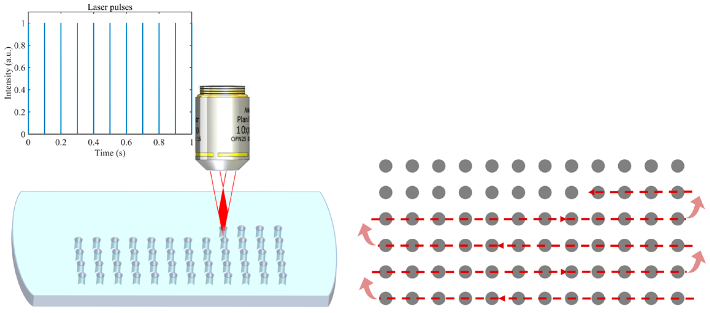
The schematic diagram in Figure 8 illustrates the fabrication method for a microhole array. It utilizes a continuous scanning approach with a piecewise linear pattern to achieve single-pulse continuous femtosecond laser processing. In this process, the lateral period is controlled by the combined effect of the displacement speed of the stage and the laser’s repetition rate, while the scanning interval determines the vertical period.
To achieve a similar size of microhole at the entrance and exit positions of the beam, a sample with a thickness of 400 μm is used. The optimal focusing position was determined pre-experiment. As shown in Figure 9a, as ΔZ gradually increases, the morphology of the microholes on the sub-surface gradually evolves towards a circular shape; on the contrary, the morphology deteriorates. This observation aligns with the conclusion drawn in Figure 7. However, when the peak power plane further penetrates the sample with ΔZ ≥ 120, a noticeable phenomenon occurs where the diameter of the microholes on the upper surface decreases and the morphology deteriorates. This can be attributed to the shorter length of region A. Comparing the processing results, in the sample with a thickness of 400 μm, microholes with approximately circular and similar diameters at the upper surface and subface can be obtained when the peak light intensity plane is located below the surface by 100 μm.
Based on the preliminary experimental results, the defocus parameter ΔZ was adjusted to 100 μm for array fabrication with a single-pulse energy of 220 μJ and a repetition rate of 40 Hz. By adjusting the movement speed of the displacement stage, the array period was controlled to be 5 μm, and it took 13.5 min to fabricate a square array measuring 0.9 × 0.9 mm (with a total of 32,761 units). As shown in Figure 9b, the colors observed in the physical image of the microhole array represent the structural colors resulting from the periodic structure. Under low magnification, the array was observed to be uniformly distributed without any noticeable defects. When observed under high magnification, the diameter of the microhole array units was measured to be approximately 1.27 μm, with an aspect ratio of 315:1. However, due to the non-uniform linear movement of the displacement stage, the array period exhibited some deviation. This study utilizes an uninterrupted line-scanning processing method, which not only exhibits the repeatability of single-pulse processing, ensuring the uniformity of each microhole in the array, but also allows for improved processing efficiency by synchronously increasing the laser repetition rate and the displacement speed of each stage. Due to platform limitations, the processing frequency is only 40 Hz. Increasing it to 1000 Hz could reduce array fabrication time to half a minute.
4. Conclusions
In summary, a method for the rapid fabrication of microhole arrays with high aspect ratios in YAG crystals using femtosecond laser single-pulse Bessel beams was demonstrated in this study. A femtosecond Bessel beam was obtained through shaping with an axicon system. The spatial distribution characteristics of the initial Bessel beam after shaping with an axicon lens were calculated, along with its relationship to the apex angle of the axicon lens. The experimental results confirmed that the femtosecond Bessel beam significantly improved the aspect ratio of the microholes fabricated in YAG crystals, achieving values several tens of times higher than those obtained with Gaussian beam processing. The influence and control mechanisms of laser power and focal plane position on the morphology and aspect ratio of microholes fabricated in YAG crystals using single-pulse femtosecond Bessel beams were investigated in this study. By adjusting the laser pulse energy within the range of 200–400 μJ, the diameter of the microholes could be controlled to a certain extent while avoiding side-lobe damage. As a result, microholes with a maximum aspect ratio of 384:1 are produced. A microhole array measuring 181 × 181 was fabricated at 40 holes per second on a sample with a thickness of 400 μm by optimizing the experimental parameters. The array had a period of 5 μm and an aspect ratio of 315:1, and the array units exhibited nearly circular morphology on both the top surface and subface with excellent repeatability. This method offers a potential means for efficiently fabricating micro–nano functional structures such as microstructured waveguides and photonic crystals in YAG crystals.
Author Contributions
Conceptualization, T.Z. and H.Y.; methodology, T.Z., Z.W. and H.Y.; software, H.Y.; validation, H.Y., L.C. and T.Z.; analysis, H.Y. and L.C.; investigation, H.Y.; resources, T.Z., B.X. and Y.Y.; data curation, H.Y. and L.C.; writing—original draft preparation, H.Y.; writing—review and editing, H.Y. and T.Z.; visualization, H.Y. and L.C.; supervision, S.M. and Z.W.; project administration, T.Z. and Z.W.; funding acquisition, T.Z. All authors have read and agreed to the published version of the manuscript.
Funding
This research was funded by the National Natural Science Foundation of China, grant number 52105423, and Beijing Municipal Commission of Education, grant number KM202210005004.
Institutional Review Board Statement
Not applicable.
Informed Consent Statement
Not applicable.
Data Availability Statement
Data are contained within the article.
Conflicts of Interest
The authors declare no conflicts of interest.
References
- Lu, Y.M.; Duan, Y.Z.; Liu, X.Q.; Chen, Q.D.; Sun, H.B. High-quality rapid laser drilling of transparent hard materials. Opt. Lett. 2022, 47, 921–924. [Google Scholar] [CrossRef]
- An, R.; Hoffman, M.D.; Donoghue, M.A.; Hunt, A.J.; Jacobson, S.C. Water-assisted femtosecond laser machining of electrospray nozzles on glass microfluidic devices. Opt. Express 2008, 16, 15206–15211. [Google Scholar] [CrossRef] [PubMed]
- Vong, T.; Schoffelen, S.; van Dongen, S.F.M.; van Beek, T.A.; Zuilhof, H.; van Hest, J.C.M. A DNA-based strategy for dynamic positional enzyme immobilization inside fused silica microchannels. Chem. Sci. 2011, 2, 1278–1285. [Google Scholar] [CrossRef]
- Leng, N.; Jiang, L.; Li, X.; Xu, C.C.; Liu, P.J.; Lu, Y.F. Femtosecond laser processing of fused silica and aluminum based on electron dynamics control by shaping pulse trains. Appl. Phys. A Mater. 2012, 109, 679–684. [Google Scholar] [CrossRef]
- Baheri, S.; Tabrizi, S.P.A.; Jubran, B.A. Film cooling effectiveness from trenched shaped and compound holes. Heat. Mass. Transfer 2008, 44, 989–998. [Google Scholar] [CrossRef]
- Fei, Z.Z.; Hu, X.; Choi, H.W.; Wang, S.N.; Farson, D.; Lee, L.J. Micronozzle Array Enhanced Sandwich Electroporation of Embryonic Stem Cells. Anal. Chem. 2010, 82, 353–358. [Google Scholar] [CrossRef] [PubMed]
- Wu, P.F.; Zhu, S.H.; Hong, M.H.; Chen, F.; Liu, H.L. Specklegram temperature sensor based on femtosecond laser inscribed depressed cladding waveguides in Nd:YAG crystal. Opt. Laser Technol. 2019, 113, 11–14. [Google Scholar] [CrossRef]
- Lai, M.F.; Li, S.W.; Shih, J.Y.; Chen, K.N. Wafer-level three-dimensional integrated circuits (3D IC): Schemes and key technologies. Microelectron. Eng. 2011, 88, 3282–3286. [Google Scholar] [CrossRef]
- Jia, C.L.; Tang, W.J.; Liu, K.; Liao, Y. Transparent Ho,Yb:YAG crystal waveguide inscribed by direct femtosecond laser writing. Opt. Mater. 2023, 135, 113314. [Google Scholar] [CrossRef]
- Egashira, K.; Mizutani, K. Micro-drilling of monocrystalline silicon using a cutting tool. Precis. Eng. 2002, 26, 263–268. [Google Scholar] [CrossRef]
- Cao, X.D.; Kim, B.H.; Chu, C.N. Micro-structuring of glass with features less than 100 μm by electrochemical discharge machining. Precis. Eng. 2009, 33, 459–465. [Google Scholar] [CrossRef]
- Ahn, S.H.; Ryu, S.H.; Choi, D.K.; Chu, C.N. Electro-chemical micro drilling using ultra short pulses. Precis. Eng. 2004, 28, 129–134. [Google Scholar] [CrossRef]
- Spinney, P.S.; Howitt, D.G.; Smith, R.L.; Collins, S.D. Nanopore formation by low-energy focused electron beam machining. Nanotechnology 2010, 21, 375301. [Google Scholar] [CrossRef]
- Sebastiani, M.; Eberl, C.; Bemporad, E.; Pharr, G.M. Depth-resolved residual stress analysis of thin coatings by a new FIB-DIC method. Mat. Sci. Eng. A-Struct. 2011, 528, 7901–7908. [Google Scholar] [CrossRef]
- Wu, J.H.; Chantiwas, R.; Amirsadeghi, A.; Soper, S.A.; Park, S. Complete plastic nanofluidic devices for DNA analysis direct imprinting with polymer stamps. Lab. Chip 2011, 11, 2984–2989. [Google Scholar] [CrossRef]
- Sugioka, K.; Cheng, Y. Fabrication of 3D microfluidic structures inside glass by femtosecond laser micromachining. Appl. Phys. A Mater. 2014, 114, 215–221. [Google Scholar] [CrossRef]
- Lu, Y.; Li, Y.F.; Wang, G.; Yu, Y.; Bai, Z.X.; Wang, Y.L.; Lu, Z.W. Femtosecond Laser Fabrication of Microchannels in Transparent Hard Materials. Adv. Mater. Technol. 2023, 8, 2300015. [Google Scholar] [CrossRef]
- Jiang, C.Y.; Zhou, G.Q.; Xu, J.; Deng, P.Z.; Gan, F.X. Femtosecond laser irradiation on YAG and sapphire crystals. J. Cryst. Growth 2004, 260, 181–185. [Google Scholar] [CrossRef]
- Liu, H.L.; de Aldana, J.R.V.; Hong, M.H.; Chen, F. Femtosecond Laser Inscribed Y-Branch. Waveguide in Nd:YAG Crystal: Fabrication and Continuous-Wave Lasing. IEEE J. Sel. Top. Quantum 2016, 22, 227–230. [Google Scholar] [CrossRef]
- Ren, Y.Y.; Zhang, L.M.; Romero, C.; de Aldana, J.R.V.; Chen, F. Femtosecond laser irradiation on Nd:YAG crystal: Surface ablation and high-spatial-frequency nanograting. Appl. Surf. Sci. 2018, 441, 372–380. [Google Scholar] [CrossRef]
- Ródenas, A.; Gu, M.; Corrielli, G.; Paiè, P.; John, S.; Kar, A.K.; Osellame, R. Three-dimensional femtosecond laser nanolithography of crystals. Nat. Photonics 2019, 13, 105–109. [Google Scholar] [CrossRef]
- Courvoisier, F.; Stoian, R.; Couairon, A. Ultrafast laser micro-and nano-processing with nondiffracting and curved beams: Invited paper for the section: Hot topics in ultrafast lasers. Opt. Laser Technol. 2016, 80, 125–137. [Google Scholar] [CrossRef]
- Meyer, R.; Jacquot, M.; Giust, R.; Safioui, J.; Rapp, L.; Furfaro, L.; Lacourt, P.A.; Dudley, J.M.; Courvoisier, F. Single-shot ultrafast laser processing of high-aspect-ratio nanochannels using elliptical Bessel beams. Opt. Lett. 2017, 42, 4307–4310. [Google Scholar] [CrossRef] [PubMed]
- Rapp, L.; Meyer, R.; Giust, R.; Furfaro, L.; Jacquot, M.; Lacourt, P.-A.; Dudley, J.M.; Courvoisier, F. High aspect ratio micro-explosions in the bulk of sapphire generated by femtosecond Bessel beams. Sci. Rep. 2016, 6, 34286. [Google Scholar] [CrossRef] [PubMed]
- Xie, Q.; Li, X.; Jiang, L.; Xia, B.; Yan, X.; Zhao, W.; Lu, Y. High-aspect-ratio, high-quality microdrilling by electron density control using a femtosecond laser Bessel beam. Appl. Phys. A 2016, 122, 136. [Google Scholar] [CrossRef]
- Chen, T.; Zhang, G.; Wang, Y.; Li, X.; Stoian, R.; Cheng, G. Reconstructing of embedded high-aspect-ratio nano-voids generated by ultrafast laser bessel beams. Micromachines 2020, 11, 671. [Google Scholar] [CrossRef] [PubMed]
- Vetter, C.; Giust, R.; Furfaro, L.; Billet, C.; Froehly, L.; Courvoisier, F. High aspect ratio structuring of glass with ultrafast Bessel beams. Materials 2021, 14, 6749. [Google Scholar] [CrossRef] [PubMed]
- Fernelius, N.C.; Graves, G.A.; Knecht, W.L. Characterization of Candidate Laser Window Materials. Proc. Soc. Photo Opt. Instrum. 1981, 297, 188–195. [Google Scholar]
- Zhang, N.; Ye, J.-S.; Feng, S.-F.; Wang, X.-K.; Han, P.; Sun, W.-F.; Zhang, Y.; Zhang, X.-C. Generation of long-distance stably propagating Bessel beams. OSA Contin. 2021, 4, 1223–1233. [Google Scholar] [CrossRef]
- Cizmár, T. Optical Traps Generated by Non-Traditional Beams. Ph.D. Thesis, Masaryk University in Brno, Brno, Czech Republic, 2006. [Google Scholar]
Figure 1.
Schematic diagram of the femtosecond laser processing system (HWP: half-wave plate; PBS: polarizing beam splitter; NDF: neutral density filter; MS: mechanical shutter; MO: microscope objective; DM: dichroic mirror; CCD: charge-coupled device image sensor; Axicon: axicon lens: L1 and L2: lenses; M1, M2: mirrors).

Figure 2.
(a) Optical photographs of Gaussian pulse processing at different repetition rates, with SEM images as insets. (b) Variation trend of damage diameter with power for Gaussian pulses at different repetition rates. (c) Optical photographs and damage depth of Gaussian beam processing with a single pulse of 100 mW. (d) Variation trend of the ratio of processing diameter to depth with power for single-pulse processing.

Figure 3.
(a) Intensity distribution in the propagation direction of the initial Bessel beam. (b) Transverse intensity distribution of the initial Bessel beam. (c) Intensity distribution in the propagation direction of the Gaussian beam. (d) Transverse intensity distribution of the Gaussian beam.
Figure 3.
(a) Intensity distribution in the propagation direction of the initial Bessel beam. (b) Transverse intensity distribution of the initial Bessel beam. (c) Intensity distribution in the propagation direction of the Gaussian beam. (d) Transverse intensity distribution of the Gaussian beam.

Figure 4.
(a) Schematic diagram of the Bessel beam generated by the axicon lens. (b) Parameters of the initial Bessel beam generated by different apex-angle axicon lenses: “No diffraction distance”. (c) Size of the central main lobe (ω = 4 mm λ = 800 nm) of the initial Bessel beam.
Figure 4.
(a) Schematic diagram of the Bessel beam generated by the axicon lens. (b) Parameters of the initial Bessel beam generated by different apex-angle axicon lenses: “No diffraction distance”. (c) Size of the central main lobe (ω = 4 mm λ = 800 nm) of the initial Bessel beam.

Figure 5.
SEM image of femtosecond Bessel beam preparation for microhole (a) at the beam entrance and (b) at the beam exit. (c) Sectional profile of micropores fabricated by Gaussian beam and Bessel beam.
Figure 5.
SEM image of femtosecond Bessel beam preparation for microhole (a) at the beam entrance and (b) at the beam exit. (c) Sectional profile of micropores fabricated by Gaussian beam and Bessel beam.

Figure 6.
The variation trend of damage diameter and surface morphology in microhole processing with different single-pulse energies.
Figure 6.
The variation trend of damage diameter and surface morphology in microhole processing with different single-pulse energies.

Figure 7.
(a) Schematic diagram of the focal length of the processing beam. (b) Schematic diagram of the interaction area of the Bessel beam and the sample with the amount of defocusing. (c) Machining results from changing the defocus amount parameters.
Figure 7.
(a) Schematic diagram of the focal length of the processing beam. (b) Schematic diagram of the interaction area of the Bessel beam and the sample with the amount of defocusing. (c) Machining results from changing the defocus amount parameters.

Figure 8.
Schematic diagram of the microhole array fabrication method.

Figure 9.
(a) Morphology images of microhole top surface and subface fabricated with different defocus amounts in a 400 μm thick sample. (b) Microscopic photograph of the microhole array.
Figure 9.
(a) Morphology images of microhole top surface and subface fabricated with different defocus amounts in a 400 μm thick sample. (b) Microscopic photograph of the microhole array.


Table 1.
Partial physical properties of YAG crystal.
| Property | Detail | Note |
|---|---|---|
| Crystal structure | Cubic | |
| Refractive index | 1.8197 | @1064 nm |
| Density | 4.55 | g/cm3 |
| Mohs hardness | 8~8.5 | |
| Thermal conductivity | 13.1 | W/m/K, @20 °C |
Disclaimer/Publisher’s Note: The statements, opinions and data contained in all publications are solely those of the individual author(s) and contributor(s) and not of MDPI and/or the editor(s). MDPI and/or the editor(s) disclaim responsibility for any injury to people or property resulting from any ideas, methods, instructions or products referred to in the content. |
© 2024 by the authors. Licensee MDPI, Basel, Switzerland. This article is an open access article distributed under the terms and conditions of the Creative Commons Attribution (CC BY) license (https://creativecommons.org/licenses/by/4.0/).
Share and Cite
MDPI and ACS Style
Yang, H.; Yu, Y.; Zhang, T.; Ma, S.; Chen, L.; Xu, B.; Wang, Z. Rapid Fabrication of Yttrium Aluminum Garnet Microhole Array Based on Femtosecond Bessel Beam. Photonics 2024, 11, 408. https://doi.org/10.3390/photonics11050408
AMA Style
Yang H, Yu Y, Zhang T, Ma S, Chen L, Xu B, Wang Z. Rapid Fabrication of Yttrium Aluminum Garnet Microhole Array Based on Femtosecond Bessel Beam. Photonics. 2024; 11(5):408. https://doi.org/10.3390/photonics11050408
Chicago/Turabian StyleYang, Heng, Yuan Yu, Tong Zhang, Shufang Ma, Lin Chen, Bingshe Xu, and Zhiyong Wang. 2024. "Rapid Fabrication of Yttrium Aluminum Garnet Microhole Array Based on Femtosecond Bessel Beam" Photonics 11, no. 5: 408. https://doi.org/10.3390/photonics11050408
Note that from the first issue of 2016, this journal uses article numbers instead of page numbers. See further details here.