
Impact of Chaos on MOSFET Thermal Stress and Lifetime


1
Ecole Supérieure des Techniques Aéronautiques et de Construction Automobile, ESTACA’Lab Paris-Saclay, 12 Avenue Paul Delouvrier, RD10, Montigny-le-Bretonneux, 78180 Paris, France
2
Electrical Engineering and Computer Science Department, University of Angers, 49045 Angers, France
*
Author to whom correspondence should be addressed.
†
Current address: Campus Ouest, Rue Georges Charpak-BP 76121, CEDEX 9, 53061 Laval, France.
‡
These authors contributed equally to this work.
Electronics 2024, 13(9), 1649; https://doi.org/10.3390/electronics13091649
Submission received: 17 March 2024
/
Revised: 16 April 2024
/
Accepted: 17 April 2024
/
Published: 25 April 2024
(This article belongs to the Special Issue Advances in Power Converter Design, Control and Applications)
Abstract
:The reliability of power electronic switching components is of great concern for many researchers. For their usage in many mission profiles, it is crucial for them to perform for the duration of their intended lifetime; however, they can fail because of thermal stress. Thus, it is essential to analyze their thermal performance. Non-linear switching action, bifurcation and chaotic events may occur in DC-DC power converters. Consequently, they show different behaviors when their parameters change. However, this is an opportunity to study these bifurcation phenomena and the existence of chaos, e.g., in boost converters, on their performance as the effects of load variations (mission profiles) on the system’s behavior. These variations generate many non-linear phenomena such as periodic behavior, repeated period-doubling bifurcations and chaos in the MOSFET drain-source current. Thus, we propose, for the first time, an analysis of the influence of chaos on the junction temperature. First of all, this paper provides a step-by-step procedure to establish an electrothermal model of a C2M0080120D MOSFET with integrated power loss. Then, the junction temperature is estimated by computing the power losses and a thermal impedance model of the switch. Additionally, this model is used to investigate the bifurcation and chaotic behavior of the MOSFET junction temperature. The paper contributes by providing a mathematical model to calculate several coefficients based on experimental data and thermal oscillations. Estimation of the number of cycles to failure is given by the Coffin–Manson equation, while temperature cycles are counted using the rainflow counting algorithm. Further, the accumulated damage results are calculated using the Miner’s model. Finally, a comparison is made between the damage accumulated during different mission profiles: significant degradation of the MOSFET’s lifetime is pointed out for chaotic currents compared to periodic ones.
1. Introduction
Today, power switching semiconductor devices such as IGBTs and MOSFETs are widely used in aerospace, transport and industrial applications. The trend towards high power density is accompanied by increasingly severe operational constraints in terms of current, voltage and temperature. Indeed, it is important to maintain the functional performance of the components in their new environment, but above all to ensure their operational safety to avoid any power device failure that could impact the entire system [1].
Among the components, power semiconductor devices are the most fragile in converters and inverters and are strongly affected by the mission profiles [2]. Thus, one approach is to adopt a realistic mission profile in order to obtain a reliable assessment of the MOSFET’s lifetime. There are daily solar irradiance profiles for photovoltaic systems [3,4], reference speed [5,6] and reference torque [5] profiles for drive motor applications and reference voltage [7] and load mission profiles [8] for electric bus applications.
Due to the strong non-linear modeling of switching converters [9], these converters can exhibit complex dynamical behaviors such as bifurcation and chaos with variation of a bifurcation parameter [10]. This bifurcation parameter can be the load [11], the reference voltage [12], the reference current [13,14], the inductance [15] of the converter, or a control parameter [16,17]. There is a bifurcation route towards chaos when increasing or decreasing these parameters, forcing the MOSFET to operate under harsh conditions. In this paper, the mission profiles are the different values of the load bifurcation parameter: load variation frequently leads to a loss of stability if the duty cycle is outside a certain range.
Generally, a MOSFET is considered an ideal switch in fast simulation in order to analyze the efficiency and reliability of power electronic systems, as in [18,19,20,21,22]. On the other hand, it is difficult to calculate the MOSFET’s power losses (which include the conduction, switching losses, diode conduction and reverse recovery losses [23]) and to take into account the effect of the junction temperature on the device parameters. In the literature, various electrothermal modeling strategies have been reported. The lookup table method is applied [24] to approximate switching as well as on-state losses of the IGBT. In [25], a more complete electrothermal model is proposed, which takes into account the junction temperature and also the electrical load as input variables. The model of [26] considers the interactions between the junction temperature and the voltages and currents of the transistor. In [27], the power losses are averaged every several switching cycles using a high-speed electrothermal model. The authors of [28,29] determine a realistic model of a DC-DC converter wherein the parameters are identified based on the component datasheets, the printed circuit board (PCB) layout and the length and diameter of the cables. Some parasitic inductances and capacitances result from the geometric structure of the circuit (e.g., the printed circuit and the cables used).
To analyze the MOSFET’s thermal behavior [30], power losses are used to deduce the junction temperature. The heat transfer model can use the Foster [31,32] or Cauer [33] networks, the finite element method or the finite difference method. In [34], a third-order Foster circuit is used to fit the impedance curve of a MOSFET given by the datasheet. In [35], 450 different electrothermal (Foster) variants are proposed to simulate an electric vehicle inverter. In [36], the junction temperature is estimated using the finite element method to reduce the duration of accelerated aging tests. With on-state voltage measurement, ref. [37] uses a Kalman filter for the junction temperature estimation of a full-bridge inverter. In [38], the resistances of the linear Cauer network are replaced by controlled voltage sources. In this way, a more realistic analysis is realized that considers the thermal coupling between power devices containing non-linear convection terms.
A real-time monitoring strategy of the junction temperature is proposed by [39]. The junction temperature distribution is not uniform, and control solutions depend on the load profile: the controller is adjusted to ensure the desired performance [40]. Active thermal control is used by [41] to adjust the thermal stress of the power device. The authors of [42] improve the thermal management in an IGBT’s structure, thus reducing the leakage current.
According to [43], changes in the power device junction temperature affect their reliability and lifetime estimations. From the thermal and aging points of view, the drain-source MOSFET resistance is influenced by the junction temperature, as in [44]. The two most common failures for power electronics devices are die-attach solder fatigue [45] and bond-wire damage caused by temperature cycling. Bond-wire damage is serious degradation of a MOSFET, while solder fatigue does not destroy the device but affects its durability. Therefore, mean junction temperature and junction temperature variation are both required for lifetime estimation.
In order to evaluate the lifetime of a MOSFET, the Coffin–Manson law is the most used model to evaluate device failure cycles. For example, in [46,47,48], the lifetime of an inverter [49] and of a multi-level converter is estimated with the rainflow counting algorithm with the mean junction temperature and the junction temperature variation as inputs.
To illustrate our method, we chose the C2M0080120D MOSFET [50] to study the influence of the junction temperature on its lifetime when the boost converter loses its stability. Therefore, a bifurcation diagram is defined to understand and analyze the stability of boost converters under different operating conditions. The load (representing the mission profile) generates many non-linear phenomena as periodic behavior, repeated period-doubling bifurcations and chaos of the MOSFET drain-source current, impacting the junction temperature. Then, a step-by-step procedure for establishing the electrothermal model of the MOSFET with integrated power loss is proposed in this paper. We highlight not only a reduction in the stable range of the junction temperature variation but also an extension of the chaos range. Additionally, we propose a mathematical model to calculate several coefficients based on experimental data and thermal swings. The estimation of the number of cycles to failure is given by the Coffin–Manson equation, while temperature cycles are counted using the rainflow counting algorithm. Accumulated damage results from the Miner’s model. This paper presents for the first time the significant impact of the overall magnitude of the current ripple for the chaos behavior, which leads to significant thermal stress. Finally, a comparison is made between the damage accumulation by different mission profiles: an important degradation of the MOSFET’s lifetime is pointed out for a chaotic current compared to a periodic one.
The main aspects of this paper are as follows: Section 2 describes the boost converter system. In Section 3, bifurcation analysis is carried out for different mission profiles. Then, in Section 4, the electrical model is detailed, followed by the power loss calculations for the MOSFET and diodes in Section 5. Thermal model simulation results are presented whereby a cascade of bifurcations doubling the stable junction temperature period is observed in Section 6. Section 7 details the lifetime model that estimates the damage to a C2M0080120D MOSFET. We end with a conclusion in Section 8.
2. Boost Converter
The schematic diagram of the boost converter circuit that uses a current loop is shown in Figure 1. The target power device is a silicon carbide (SiC) C2M0080120D MOSFET transistor. The circuit has two states determined by the state of the transistor. The MOSFET is controlled by an latch. A clock pulse of period T sets the latch at the beginning of every cycle, turning on the MOSFET: the inductance current i increases. denotes the reference peak inductor current . When i exceeds the value of , the latch is reset and the switch is turned off. The switch again turns on at the beginning of the next clock pulse. The capacitor voltage v and the inductor current i are the state variables of the circuit. The boost converter operating in continuous mode is described by two sets of linear differential equations as:
- MOSFET switch on:
- MOSFET switch off:
Equations (1) and (2) solve for the the currents and voltages across the components. An electrothermal model is developed based on the power module configuration. For the electrical model of the boost converter, Figure 1 depicts the conduction and switching power loss blocs of the MOSFET and diode generated for a selected mission profile. Then, losses are injected into the thermal model for the calculation of the device junction temperature . The estimated provides feedback for power loss computations, which it affects at each next time step.
The simulations are made with the SimScape toolbox of MATLAB R2020b Simulink and include the boost converter with its control strategy (peak current control); the power losses and thermal model are MATLAB Simulink subsystems.
3. Non-Linear Behavior and Bifurcation Analysis of the Boost Converter
In this section, we present the dynamical behavior and bifurcation diagram of the boost converter with the current mode control. Figure 2, Figure 3 and Figure 4 show the simulation results of inductance current obtained with the load resistance R as the bifurcation parameter. R is varied over the range 5 –20 without a thermal effect.
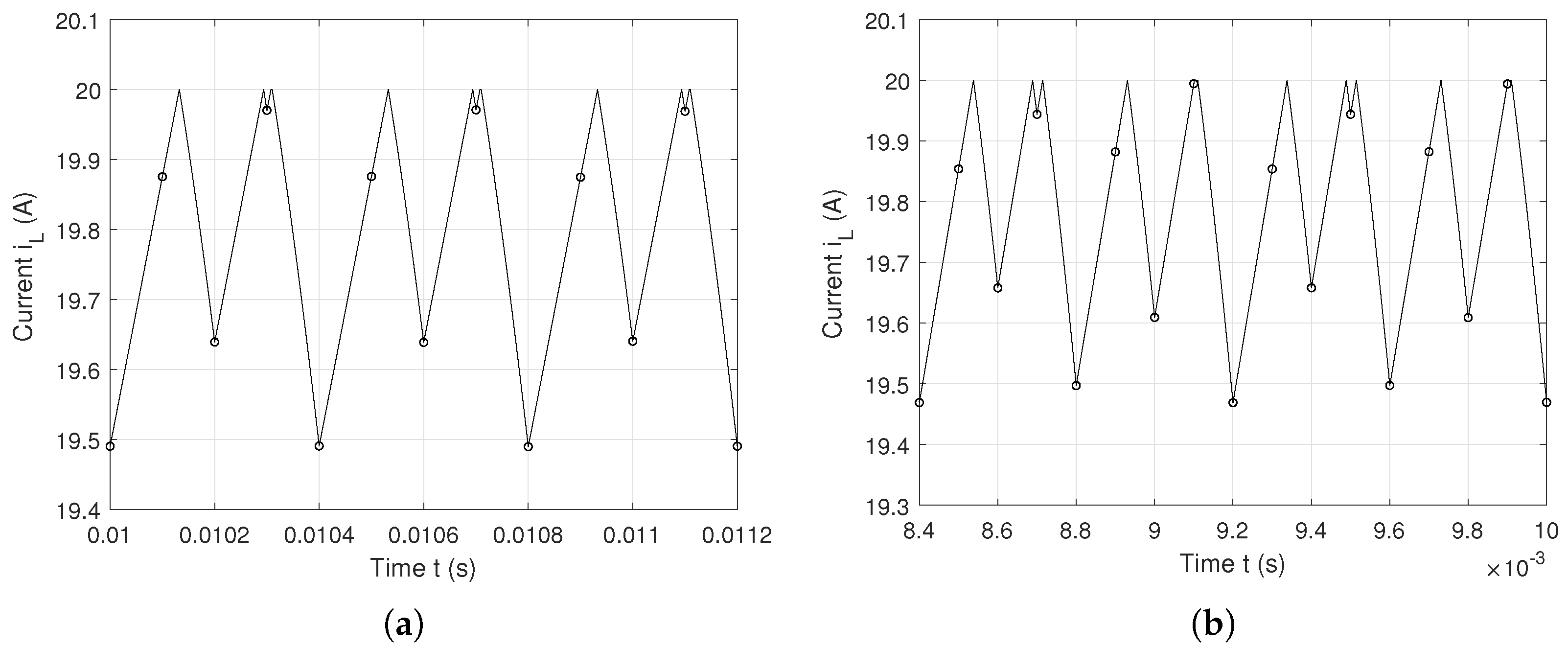
A cascade of period-doubling bifurcations of stable cycles is observed in the system. Figure 2a presents a stable limit cycle (period-one T response). With a further increase in R parameter values (from R = 6 to 8 ), a stable limit cycle of a double period 2T is observed in Figure 2b. A stable cycle of period four emerges at R = 13.1 , and at R = 13.8 , there is a stable cycle of period eight (Figure 3). For higher values of the bifurcation parameter R, the system reveals a sequence of stable cycles of a subharmonic cascade of bifurcations. For R = 15.2 , the system is attracted to the period-six T orbit, as in Figure 4a. If the value of R is further increased, the system is stroked by a border collision before it goes into chaos (Figure 4b). Obviously, in a chaotic state, the system operates with large values of inductance current .
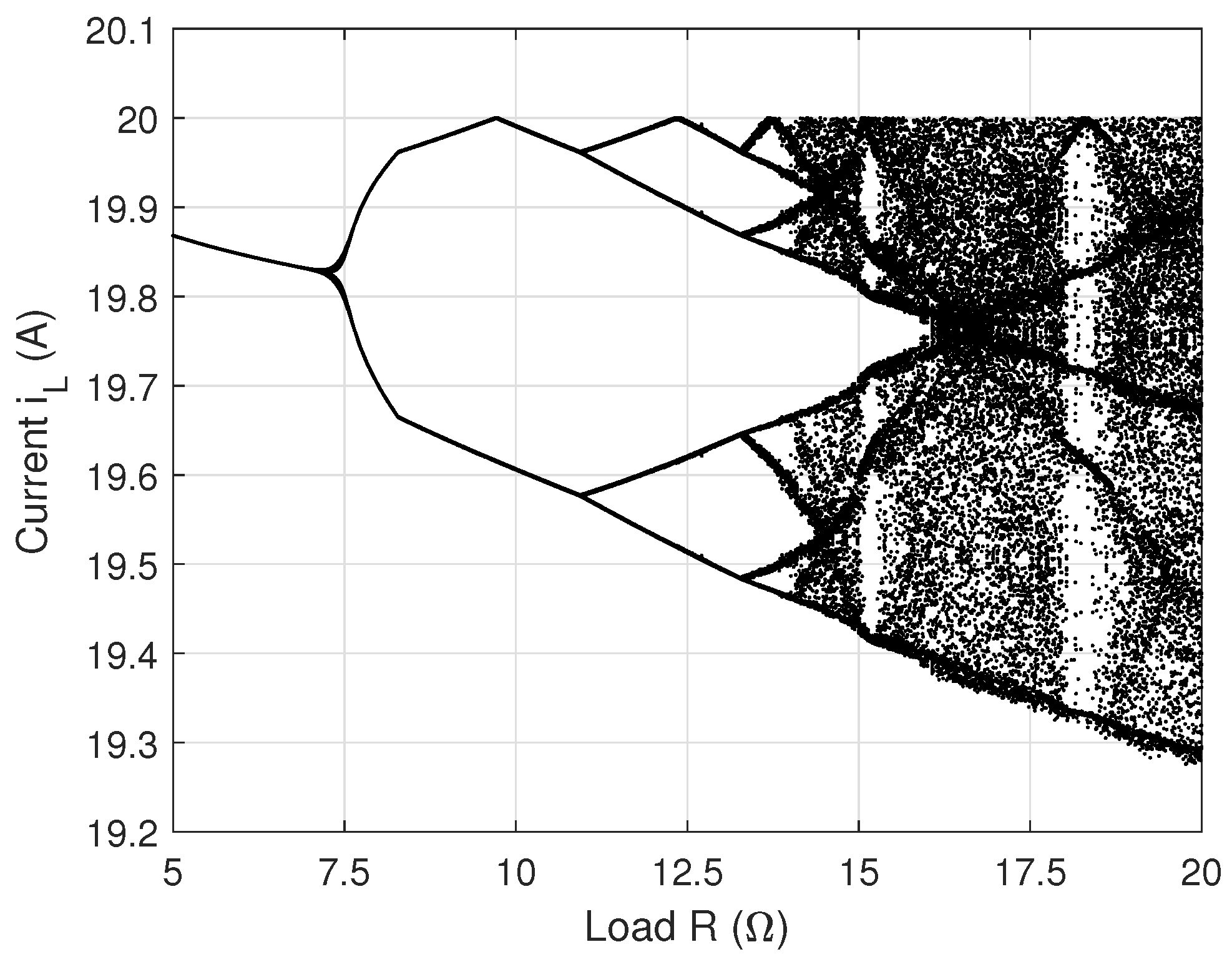
A bifurcation diagram represents all the plots of the steady-state orbit as a function of the bifurcation parameters. We vary the load resistance R parameter and plot hundreds of consecutive values of the inductance current at each clock period T. The bifurcation diagram is presented in Figure 5: the period-doubling bifurcation occurs at R = 7.32 and changes the steady-state behavior of the system. Along with the increase in R, the converter undergoes several period-doubling bifurcations and eventually evolves into a chaotic state. For different values of R, one can easily identify the boost converter behavior: the system is periodic for small values of R while it is chaotic for large values of R. It is essential to study the occurrence of chaos due to the variation of system parameters to predict non-linear phenomena and to size components for correct operation. These six values of R (6 , 8 , 13.1 , 13.8 , 15.2 and 20 ) are used to generate the load profiles.
4. Electrical MOSFET Model
Power semiconductors are non-ideal transistors because of their parasitics, such as source inductance , drain inductance , and gate inductance and parasitic capacitances , and , as shown in Figure 6. Their real electric model takes into consideration the source resistance , drain resistance , gate resistance and drain-source resistance .
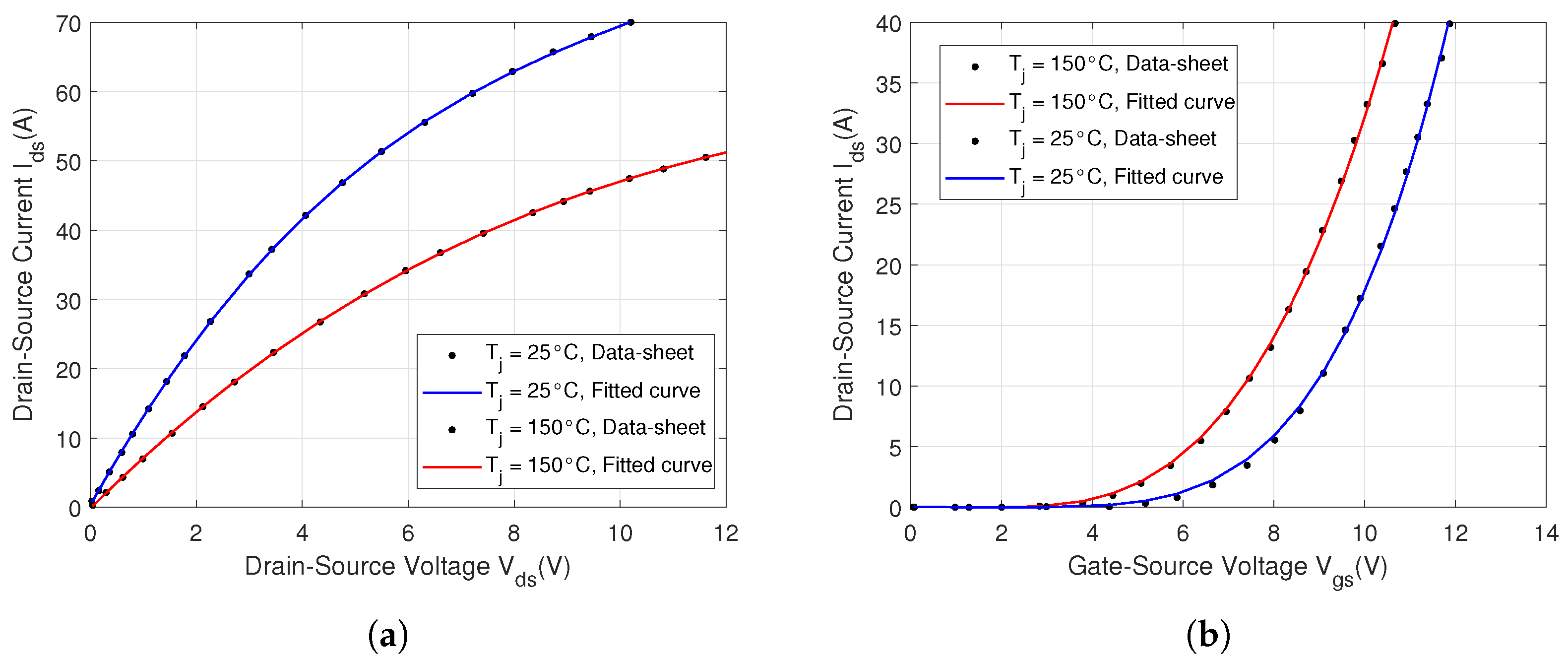
Some MOSFET parameters have been extracted from electrical characteristics (from static current–voltage characteristics - and -) and the reverse diode from the C2M0080120D MOSFET datasheet (the point curves of Figure 7). All these parameters (resistances, inductances and capacitances) are required by the SimScape MOSFET model. Herein, the MOSFET model using MATLAB Simulink is based on the Shichman–Hodges model. The Shichman–Hodges model takes channel length modulation into account and uses a controlled current source to describe the drain-source current . In order to reproduce these two characteristics, the Shichman–Hodges model describes the three operational regions of the MOSFET (off, linear and saturation) by three distinct equations given below:
where is the threshold voltage, k is the transistor gain, and is the channel length modulation.
Based on the static current–voltage characteristics shown in Figure 7a, the following polynomial fitting functions are used to obtain fitted simulation curves of - at two different junction temperatures :
The coefficients of the - curves are fitted using a MATLAB curve-fit tool. Figure 7b displays the static current–voltage characteristics - described by the following polynomial fitting functions:
In order to verify the accuracy of the MOSFET electrical model, these static characteristics obtained by simulation are compared with the ones from the datasheet; the characteristics are reported together in Figure 7a,b, respectively, for 25 °C and 150 °C. Indeed, these curves are very close to each other over the full operating range.
5. Power Loss Computation
The MOSFET produces power losses, which can be distinguished as conduction loss and switching loss. Figure 1 presents also the power losses for the diode. Addition of all losses computes the total power loss.
5.1. MOSFET Power Loss Computation
The conduction power loss at each time step can be calculated as the product of the drain-source current through the MOSFET during conduction and the drain-source voltage across it, as shown in:
Using the static current–voltage characteristics - (Figure 7a), the fittype and fit MATLAB functions determine the voltage at two different temperatures, 25 °C and 150 °C, as in the following equations:
For many manufacturer datasheets, the dependence of switching energy losses on temperature, current or voltage is passed over. For example, the C2M0080120D datasheet gives the energy switching loss for two values of drain-source voltage (600 V and 800 V) at 20 °C and for a large variation of drain-source currents. The manufacturer datasheet also provides the energy switching loss for a large variation of the junction temperature at a drain-source current of 20 A and drain-source voltage of 800 V. The lookup table interpolates these know values in order to generate the switching energy losses at different data points as a function of the mission profiles.
The lookup table method is applied to approximate conduction as well as switching losses of the MOSFET and diode. A 2-D lookup table having vectors of temperature and current as breakpoint inputs interpolates the voltage at any and values. Based on Equations (9) and (10), the 2-D lookup table of is represented as Figure 8a. Then, the instantaneous conduction power loss of the MOSFET is calculated as the product between and .
The C2M0080120D MOSFET datasheet presents two switching loss energies: (J) and (J)—the device turn-on and turn-off energies, respectively, for junction temperatures of both = 25 °C and = 800 V, as shown in Figure 9a. These two energies are calculated using the rise and fall times of the drain-source current and voltage.
The fitting functions of the datasheet points represented in this figure are
The datasheet also presents the variation of the switching loss energies and as a function of the junction temperature (Figure 9b). For = 20 A and = 800 V, the polynomial fitting functions give a linear variation as:
A comparison of the simulation results (based on Equations (11) and (12)) and the datasheet points is shown in Figure 9a for varying drain-source current . Figure 9b presents the same switching loss energies with variation. A good match is found for both turn-on and turn-off energy losses for the case of datasheet points and simulation results (based on Equation (13)) with variation.
and depend on three variable functions of , and . Based on Equations (11) and (13), a 3-D lookup table having the temperature and the current as inputs (MATLAB breakpoints of 3-D lookup table) and as the output interpolates the switching loss energies at any , and values for the state MOSFET turn-on (Figure 8b).
Another 3-D lookup table (Figure 8c) is used to predict the switching loss energies with , and as inputs based on Equations (12) and (13). and at 25 °C and 150 °C, presented in Figure 10, are used to estimate switching losses. The instantaneous switching power loss of the MOSFET is then calculated as the product of the loss energies and the switching frequency.
5.2. Diode Power Loss Computation
Calculating the conduction loss of a body diode is similar to its calculation for a MOSFET. The following equations present the diode conduction loss as:
where represents the forward saturation voltage, and represents the forward saturation current. These two variables can be extracted from the datasheet and are indicated as datasheet points in Figure 11 for two different temperatures ( = 25 °C and = 150 °C).
Figure 11a shows a comparison of datasheet points and fitted curves obtained using the following polynomial fitting functions:
A 2-D lookup table (represented in Figure 11) has the temperature and the current as breakpoint inputs and as the output: it interpolates the voltage for any and values. Then, the instantaneous MOSFET conduction power loss is calculated as the product of and .
The diode contributes to switching energy as a result of reverse recovery charge during turn-off of the MOSFET. In [23], the analytical model of the diode switching energy depends on the peak reserve recovery current , the junction temperature and the diode forward saturation voltage . Furthermore, the slope of the diode turn-off current depends on the switching rates. The peak reverse recovery current is a function of the turn-off switching rate (), the reverse recovery charge and the snappiness factor S as follows:
The snappiness factor S is calculated with specific information from the datasheet: (25 °C) = 152 nC and / = 1950 A/s, giving S = 4.928. S is considered constant for different operating conditions. In order to calculate at = 125 °C, the following relation is used:
where / = 1090 A/s. The reverse recovery charge is 271.93 nC. Equation (19) is used to simulate the effect of the temperature on the reverse recovery charge :
Then, the energy switching loss is defined as the product of and . Figure 12a represents at 25 °C and 150 °C. A 3-D lookup table with breakpoint inputs , and calculates by interpolation the switching loss energies , as shown in Figure 12b. The instantaneous diode switching power loss is then calculated as the product of the loss energies and the switching frequency. Finally, the total power loss is the sum of all power losses.
6. Thermal Model
The thermal behavior of a MOSFET can be predicted with a resistor and capacitor thermal network. There are two conventional thermal networks that can equivalently represent the thermal performance of a MOSFET: Foster and Cauer. Due to its simplicity, almost all semiconductors use the Foster network. The thermal model of a SiC C2M0080120D MOSFET represented as an network is derived from the thermal impedance. The total power losses are passed through the Foster network and result in the device junction temperature. The junction temperature is estimated by:
where is the thermal impedance, and is the ambient temperature. According to Equation (20), computation of the junction temperature requires knowledge of the thermal impedance . is graphically provided in the datasheet of the C2M0080120D MOSFET, as shown in Figure 13. The Foster thermal network is achieved by implementing a curve-fitting identification. The parameters of the Foster model are summarized in Table 1: it contains four branches to maintain consistency with the original data from the manufacturers.
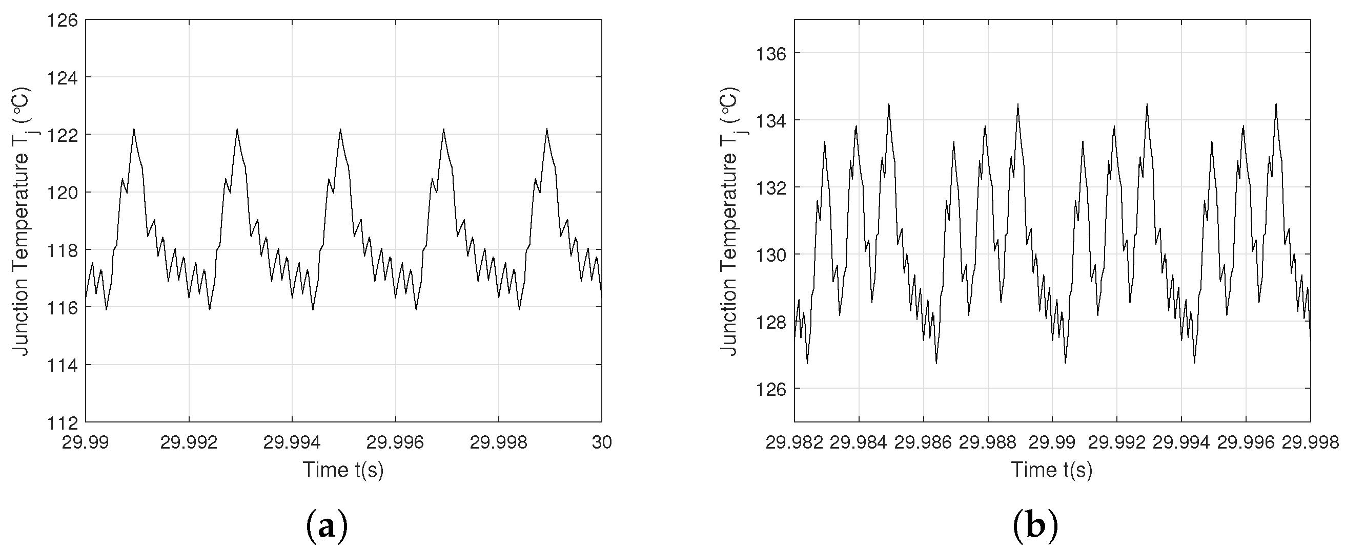
Different load values represent a typical load mission profile of the electrical boost converter. After evaluation of the corresponding power losses, the thermal model of the MOSFET produces the thermal profile shown in Figure 14, Figure 15 and Figure 16. Figure 14a presents a stable limit cycle of junction temperature for a load profile R = 6 . The time waveform is a 1T limit cycle for inductance current (Figure 2a) when the thermal conditions are passed over. With a further increase in parameter R (from 6 to R = 8 ), a stable limit cycle of a double period 2T is observed in Figure 12b, as for in Figure 2b. On the other hand, if the load increases to R = 13.1 , the junction temperature does not follow the same behavior as (stable period-4T operation as in Figure 3a), instead keeping a stable limit cycle with a 2T period. This demonstrates that the temperature influences the behavior of the converter. At R = 13.8 , the stable cycle of period 8T (Figure 3b) is divided by two. Indeed, is attracted to the period 4-T orbit, as can be seen in Figure 15b. If the value of R is further increased, the system is stroked by a border collision before it goes into chaos (Figure 16a,b).
Therefore, the temperature has an influence on the behavior of the converter: the period-doubling bifurcation is restrictive, causing chaos to appear earlier, i.e., for lower values of R. Additionally, for the six mission profiles, the junction temperature variations increase from an extremely small (less than 0.5 °C) to a large (greater than 18 °C). It is the same for the mean junction temperature: increases from 88.17 °C to 127.39 °C.
7. Lifetime Analytical Model
An accelerated power cycling test has been designed and executed to collect failure data. For this purpose, the jumps in junction temperature and the mean junction temperature are the main stress factors of the power device. It can be noted that device performance degradation differs from one device to another due to small discrepancies in device manufacturing parameters. In order to determine the qualitative behavior of the C2M0080120D, three MOSFETs are exposed to multitude power cycles under the same conditions. The experimental test represents a long cycle time: the MOSFET is turned on for 4 s and turned off for 12 s. The constant current value is intended to maintain the temperature at 125 °C. The datasheet characteristics - and - (Figure 7) present variations between different devices of the same type. Therefore, variability exists between the mean and swing junction temperatures of the tested MOSFETs. The temperatures obtained during three experimental tests to determine the heating behaviors were: = 127 °C and = 16 °C, = 126.5 °C and = 14.5 °C and = 114.2 °C and = 12.5 °C. According to the test conditions, device failure was recorded after = 8640 cycles, = 12,270 cycles and = 25,400 cycles.
These results are used to derive the experimental coefficients A and and also the activation energy . The Coffin–Manson equation is used to estimate the device failure cycles. The lifetime model of the power device for the first test can be expressed as
where is the number of cycles to failure for a certain thermal stress, and k is the Boltzmann constant (8.617 × eV/K). For the second and third tests, the Coffin–Manson models are
The coefficients A, and are calculated from Equations (21) and (22). Applying the natural logarithm, these exponential functions (21) and (22) can be expressed in linear forms. Eliminating the unknown constant A, we can write
and
Then,
Consequently, the development of can be represented by
Hence, the thermal activation energy can be calculated from
The last coefficient can be written as
Using the three experimental test datasets and according to relations (26)–(28), the following numerical values are obtained: = −4.4887, = 0.0667 and A = 2.8823 × . Hence, the calculated values are: for the first profile = 0.52 °C, = 88.17 °C; so = 4.7158 × cycles; according to = 0.9242 °C, = 106.9 °C, is found to be 3.14813 × cycles; = 2.3953 × cycles as calculated for = 7.5473 °C, = 118 °C; using = 9.4772 °C, = 129.7 °C, a failure cycle number of = 8.1376 × is found; is 1.8654 × for = 13.24 °C, = 123.96 °C; for the last profile, = 2986 cycles, where = 19.84 °C, = 127.4 °C.
In order to predict the lifetime of a power MOSFET, a thermal cycle counting algorithm is required, especially when the MOSFET operates with a variable load. Due its low error compared to other counting methods, rainflow counting is the most widely adopted method. A rainflow counting algorithm translates complicated and irregular stress profiles (time series of the junction temperature) into a set of organized cycles to facilitate the lifetime prediction for MOSFETs, especially when the converter operates with varying loads.
The basic sequence of the rainflow algorithm includes the four following steps. Firstly, the peaks and valleys of the junction temperature are extracted in order to construct linear connections. For the second step, the junction temperature undergoes a rotation of the time axis by 90° such that the plot has the shape of a pagoda, as in Figure 17. This figure plots the virtual water traces (the red and blue lines) with the origins on each peak and valley. Then, the end of the trace occurs by merging it with a virtual water trace from a higher peak or lower valley or by reaching a peak for which its opposite peak is higher and the valley is lower. The final step is to couple half cycles to full cycles. The number of cycles to failure for each mission profile is extracted by the rainflow algorithm and is presented in Figure 18, Figure 19 and Figure 20.
For simple periodic mission profiles as shown in Figure 18a, the counting algorithm is not very useful since the cycles are easily determined. However, in cases of aperiodic mission profiles, the use of counting algorithms such as rainflow is very efficient for extracting the cycles. The complete thermal profiles contain a large number of thermal cycles from the first mission profile (Figure 18), on the order of 8.5 × cycles, whereas the last mission profile (Figure 20) has a relatively small number of thermal cycles (1956 cycles).
Another important factor in lifetime estimation is the accumulated stress Q of the MOSFET, which evaluates the accumulated stress after a number of thermal cycles. Q is appraised using the Miner’s rule. It is evaluated as:
where represents the number of cycles calculated using the rainflow counting algorithm, and is the number of cycles to failure at a particular stress condition using Equation (21). With the help of the Miner’s rule, degradation of a semiconductor and its remaining lifetime can be extracted, as in Table 2.
The accumulated damage is insignificant for lower values of load (6 and 8 ), indicating a small impact due to the mission profile on the MOSFET’s lifetime. However, only a small damage increase is observed when the load is raised to 13.1 . The mission profile begins to have a strong impact on the reliability assessment of the MOSFET for a load bigger than 13.1 : for example, at 13.8 , the junction temperature behavior overbalances to a stable period-4T operation. The repercussions of the chaotic mission profile are significant for the thermal stress and the reliability performance of a MOSFET: the accumulated fatigue is 10% to 65% more than the results from the reduced profile.
8. Conclusions
In this paper, the impacts of mission profiles on the thermal stress of a MOSFET and on its lifetime have been investigated. Several mission profiles from stable 1T-period to chaotic behavior have been considered. The results indicate that chaotic mission profiles have a strong impact on the swing current amplitude of the MOSFET and on the junction temperature (especially for large values of load). Taking into account the impact of large load values into the bifurcation diagram and the junction temperature, a reduction in the stable range of the load variation was highlighted together with an extension of the chaos range. We also proposed a mathematical model to calculate several coefficients based on experimental data and thermal swings and then used it to calculate the failure cycles. This paper presents the significant impact of the overall magnitude of the current ripple for the chaos behavior, leading to large thermal stress. Finally, a comparison is made between the amounts of damage accumulation for different mission profiles: we point out a non-negligible degradation of the MOSFET’s lifetime for chaotic (reducing it by half) compared to periodic current behavior.
Author Contributions
Formulation done by C.M. Problem solved by C.M. All authors contributed equally for numerical computations, results, discussion and writing of the manuscript. Revision done by C.M. and J.-Y.M. All authors have read and agreed to the published version of the manuscript.
Funding
This research received no external funding.
Data Availability Statement
The data are available upon request to the corresponding author.
Conflicts of Interest
The authors declare no conflict of interest.
References
- Hu, Z.; Zhang, W.; Wu, J. An Improved Electro-Thermal Model to Estimate the Junction Temperature of IGBT Module. Electronics 2019, 8, 1066. [Google Scholar] [CrossRef]
- Silva, R.P.; de Barros, R.C.; Brito, E.M.S.; Boaventura, W.C.; Cupertino, A.F.; Pereira, H.A. Pursuing computationally efficient wear-out prediction of PV inverters: The role of the mission profile resolution. Microelectron. Reliab. 2020, 110, 113679. [Google Scholar] [CrossRef]
- Sangwongwanich, A.; Zhou, D.; Liivik, E.; Blaabjerg, F. Mission profile resolution impacts on the thermal stress and reliability of power devices in PV inverters. Microelectron. Reliab. 2018, 88–90, 1003–1007. [Google Scholar] [CrossRef]
- Liu, Y.; Tolbert, L.M.; Kritprajun, P.; Dong, J.; Zhu, L.; Ollis, T.B.; Schneider, K.P.; Prabakar, K. Fast Quasi-Static Time-Series Simulation for Accurate PV Inverter Semiconductor Fatigue Analysis with a Long-Term Solar Profile. Energies 2022, 15, 9104. [Google Scholar] [CrossRef]
- Barbagallo, C.; Rizzo, S.A.; Scelba, G.; Scarcella, G.; Cacciato, M. On the Lifetime Estimation of SiC Power MOSFETs for Motor Drive Applications. Electronics 2021, 10, 324. [Google Scholar] [CrossRef]
- Rasool, H.; El Baghdadi, M.; Rauf, A.M.; Zhaksylyk, A.; D’hondt, T.; Sarrazin, M.; Hegazy, O. Accurate Electro-Thermal Computational Model Design and Validation for Inverters of Automotive Electric Drivetrain Applications. Appl. Sci. 2022, 12, 5593. [Google Scholar] [CrossRef]
- Rasool, H.; Verbrugge, B.; Zhaksylyk, A.; Tran, T.M.; El Baghdadi, M.; Geury, T.; Hegazy, O. Design Optimization and Electro-Thermal Modeling of an Off-Board Charging System for Electric Bus Applications. IEEE Access 2021, 8, 84501–84519. [Google Scholar] [CrossRef]
- Cheng, T.; Lu, D.D.-C.; Siwakoti, P. A MOSFET SPICE Model with Integrated Electro-Thermal Averaged Modeling, Aging, and Lifetime Estimation. IEEE Access 2021, 9, 5545–5554. [Google Scholar] [CrossRef]
- Chen, Y.; Xie, F.; Zhang, H.; Qiu, D.; Chen, X.; Li, Z.; Zhang, G. Improvement of Stability in a PCM-Controlled Boost Converter with the Target Period Orbit-Tracking Method. Electronics 2019, 8, 1432. [Google Scholar] [CrossRef]
- Chen, X.; Long, X.; Hu, W.; Xie, B. Bifurcation and chaos behaviors of Lyapunov function controlled PWM boost converter. Energy Rep. 2021, 7, 163–168. [Google Scholar] [CrossRef]
- Morel, C.; Akrad, A.; Sehab, R.; Azib, T.; Larouci, C. Open-Circuit Fault-Tolerant Strategy for Interleaved Boost Converters via Filippov Method. Energies 2022, 15, 352. [Google Scholar] [CrossRef]
- Morel, C.; Morel, J.-Y.; Danca, M.F. Generalization of the Filippov method for systems with a large periodic input. Math. Comput. Simul. 2018, 146, 1–13. [Google Scholar] [CrossRef]
- Zamani, N.; Ataei, M.; Niroomand, M. Analysis and control of chaotic behavior in boost converter by ramp compensation based on Lyapunov exponents assignment: Theoretical and experimental investigation. Chaos Soliton Fractals 2015, 81, 20–29. [Google Scholar] [CrossRef]
- Dhifaou, R.; Brahmi, H. Fast Simulation and Chaos Investigation of a DC-DC Boost Inverter. Complexity 2021, 2021, 9162259. [Google Scholar] [CrossRef]
- Ghosh, A.; Banerjee, S.; Basak, S.; Chakraborty, C. A study of chaos and bifurcation of a current mode controlled flyback converter. In Proceedings of the IEEE 23rd International Symposium on Industrial Electronics (ISIE), Istanbul, Turkey, 1–4 June 2014. [Google Scholar]
- Trujillo, S.C.; Candelo-Becerra, J.E.; Hoyos, F.E. Analysis and Control of Chaos in the Boost Converter with ZAD, FPIC, and TDAS. Symmetry 2022, 14, 13170. [Google Scholar] [CrossRef]
- Morel, C.; Vlad, R.C.; Morel, J.-Y. Similarities between the Lorenz Related Systems. Nonlinear Dyn. Syst. Theory 2022, 22, 66–81. [Google Scholar]
- Zheng, J.; Zheng, Z.; Xu, H.; Liu, W.; Zeng, Y. Accurate Time-segmented Loss Model for SiC MOSFETs in Electro-thermal Multi-Rate Simulation. arXiv 2023, arXiv:2311.07029. [Google Scholar]
- Zheng, J.; Zheng, Z.; Xu, H.; Liu, W.; Zeng, Y. An Event-Driven Real-Time Simulation for Power Electronics Systems Based on Discrete Hybrid Time-Step Algorithm. IEEE Trans. Ind. Electron. 2023, 70, 4809–4819. [Google Scholar] [CrossRef]
- Zheng, J.; Zheng, Z.; Xu, H.; Liu, W.; Zeng, Y. An Event-Driven Parallel Acceleration Real-Time Simulation for Power Electronic Systems without Simulation Distortion in Circuit Partitioning. IEEE Trans. Power Electron. 2022, 37, 15626–15640. [Google Scholar] [CrossRef]
- Zheng, J.; Zheng, Z.; Xu, H.; Liu, W.; Zeng, Y. A Semi-implicit Parallel Leapfrog Solver with HalfStep Sampling Technique for FPGA-based Real-time HIL Simulation of Power Converters. IEEE Trans. Ind. Electron. 2023, 37, 1–10. [Google Scholar]
- Zheng, J.; Zheng, Z.; Xu, H.; Liu, W.; Zeng, Y. MPSoC-Based Dynamic Adjustable Time-Stepping Scheme with Switch Event Oversampling Technique for Real-time HIL Simulation of Power Converters. IEEE Trans. Transp. Electrif. 2023. [Google Scholar] [CrossRef]
- Jahdi, S.; Alatise, O.; Ran, L.; Mawby, P. Accurate analytical modeling for switching energy of PiN diodes reverse recovery. IET Elect. Power Appl. 2015, 62, 1461–1470. [Google Scholar] [CrossRef]
- Zhaksylyk, A.; Rauf, A.-M.; Chakraborty, S.; El Baghdadi, M.; Geury, T.; Ciglaric, S.; Hegazy, O. Evaluation of Model Predictive Control for IPMSM Using High-Fidelity Electro-Thermal Model of Inverter for Electric Vehicle Applications. Proc. SAE WCX Digit. 2021, 37, 290–295. [Google Scholar]
- Ma, K.; Bahman, A.S.; Beczkowski, S.; Blaabjerg, F. Complete Loss and Thermal Model of Power Semiconductors Including Device Rating Information. IEEE Trans. Power Electron. 2015, 30, 290–295. [Google Scholar] [CrossRef]
- Górecki, K.; Zarębski, J.; Górecki, P. Influence of Thermal Phenomena on the Characteristics of Selected Electronics Networks. Energies 2021, 14, 4750. [Google Scholar] [CrossRef]
- Zhou, Z.; Kanniche, M.S.; Butcup, S.G.; Igic, P. High-speed electrothermal simulation model of inverter power modules for hybrid vehicles. IEEE Trans. Ind. Electron. 2011, 5, 636–643. [Google Scholar]
- Górecki, P.; Wojciechowski, D. Accurate Electrothermal Modeling of High Frequency DC–DC Converters with Discrete IGBTs in PLECS Software. IEEE Trans. Ind. Electron. 2023, 70, 5739–5746. [Google Scholar] [CrossRef]
- Górecki, P.; d’Alessandro, V. A Datasheet-Driven Electrothermal Averaged Model of a Diode–MOSFET Switch for Fast Simulations of DC–DC Converters. Electronics 2024, 13, 154. [Google Scholar] [CrossRef]
- Morel, C.; Rizoug, N. Electro-Thermal Modeling, Aging and Lifetime Estimation of Power Electronic MOSFETs. Civ. Eng. Res. J. 2022, 14, 555879. [Google Scholar] [CrossRef]
- Karami, M.; Li, T.; Tallam, R.; Cuzner, R. Thermal Characterization of SiC Modules for Variable Frequency Drives. IEEE Open J. Power Electron. 2021, 2, 336–345. [Google Scholar] [CrossRef]
- Chen, H.; Lin, S.; Liu, Y. Transient electro-thermal coupled modeling of three-phase power MOSFET inverter during load cycles. Materials 2021, 14, 5427. [Google Scholar] [CrossRef] [PubMed]
- Lemmens, J.; Vanassche, P.; Driesen, J. Optimal control of traction motor drives under electrothermal constraints. IEEE J. Emerg. Sel. Top. Power Electron. 2014, 2, 249–262. [Google Scholar] [CrossRef]
- Nayak, D.P.; Pramanick, S.K. Implementation of an Electro-Thermal Model for Junction Temperature Estimation in a SiC MOSFET Based DC/DC Converter. CPSS Trans. Power Electron. Appl. 2023, 8, 42–53. [Google Scholar] [CrossRef]
- Urkizu, J.; Mazura, M.; Alacano, A.; Aizpuru, I.; Chakraborty, S. Electric vehicle inverter electro-thermal models oriented to simulation speed and accuracy multi-objective targets. Energies 2019, 12, 3608. [Google Scholar] [CrossRef]
- Hsu, F.M.; Su, Y.F.; Chiang, K.N. Determination of the junction temperature of Gallium Nitride (GaN)-based high power LED under thermal with current loading conditions. In Proceedings of the 2015 International Conference on Electronic Packaging and iMAPS All Asia Conference (ICEP-IAAC), Kyoto, Japan, 14–17 April 2015; pp. 691–694. [Google Scholar]
- Eleffendi, M.A.; Johnson, C.M. Application of Kalman filter to estimate junction temperature in IGBT power modules. IEEE Trans. Power Electron. 2015, 31, 1576–1587. [Google Scholar] [CrossRef]
- Górecki, P.; Górecki, K. Non-linear compact thermal model of IGBTs. In Proceedings of the 21st European Microelectronics and Packaging Conference (EMPC) and Exhibition, Warsaw, Poland, 10–13 September 2017. [Google Scholar]
- Di Napoli, F.; Magnani, A.; Coppola, M.; Guerriero, P.; D’Alessandro, V.; Codecasa, L.; Tricoli, P.; Daliento, S. On-Line Junction Temperature Monitoring of Switching Devices with Dynamic Compact Thermal Models Extracted with Model Order Reduction. Energies 2017, 10, 189. [Google Scholar] [CrossRef]
- Andresen, M.; Ma, K.; Buticchi, G.; Falck, J.; Blaabjerg, F.; Liserre, M. Junction temperature control for more reliable power electronics. IEEE Trans. Power Electron. 2017, 33, 765–776. [Google Scholar] [CrossRef]
- Murdock, D.; Torres, J.; Connors, J.; Lorenz, R. Active thermal control of power electronic modules. IEEE Trans. Ind. Appl. 2006, 42, 552–558. [Google Scholar] [CrossRef]
- Toulon, G.; Bourennane, A.; Isoird, K. Analysis in commutation of a new high voltage thyristor structure for high temperature. In Proceedings of the 20th International Conference Mixed Design of Integrated Circuits and Systems-MIXDES, Gdynia, Poland, 20–22 June 2013; pp. 426–430. [Google Scholar]
- Cao, R. A Thermal Modeling of Power Semiconductor Devices with Heat Sink Considering Ambient Temperature Dynamic. In Proceedings of the IEEE 9th International Power Electronics and Motion Control Conference (IPEMC2020-ECCE Asia), Nanjing, China, 29 November 2020–2 December 2020; Volume 37, pp. 290–295. [Google Scholar]
- Khorasani, R.R.; Farzamkia, S.; Wu, F.; Khoshkbar-Sadigh, A.; Brady, M.F.; Dargahi, V. Power Loss Modeling and Thermal Comparison of SiC-MOSFET-Based 2-level Inverter and 3-level Flying Capacitor Multicell Inverter. In Proceedings of the 2021 IEEE Applied Power Electronics Conference and Exposition (APEC), Phoenix, AZ, USA, 14–17 June 2021; pp. 2607–2612. [Google Scholar]
- Lai, W.; Chen, M.; Ran, L.; Xu, S.; Jiang, N.; Wang, X.; Alatise, O.; Mawby, P. Experimental investigation on the effects of narrow junction temperature cycles on die-attach solder layer in an IGBT module. IEEE Trans. Power Electron. 2017, 32, 1431–1441. [Google Scholar] [CrossRef]
- Sangwongwanich, A.; Yang, Y.; Sera, D.; Blaabjerg, F. Lifetime Evaluation of Grid-Connected PV Inverters Considering Panel Degradation Rates and Installation Sites. IEEE Trans. Power Electron. 2018, 33, 1225–1236. [Google Scholar] [CrossRef]
- Shen, Y.; Chub, A.; Wang, H.; Vinnikov, D.; Liivik, E.; Blaabjerg, F. Wear-Out Failure Analysis of an Impedance-Source PV Microinverter Based on System-Level Electrothermal Modeling. IEEE Trans. Ind. Power Electron. 2019, 66, 3914–3927. [Google Scholar] [CrossRef]
- Shipurkar, U.; Lyrakis, E.; Ma, K.; Polinder, H.; Ferreira, J.A. Lifetime Comparison of Power Semiconductors in Three-Level Converters for 10-MW Wind Turbine Systems. IEEE J. Emerg. Sel. Top. Power Electron. 2018, 6, 1366–1377. [Google Scholar] [CrossRef]
- Kishor, Y.; Patel, R. Thermal modeling and reliability analysis of recently introduced high gain converters for PV application. Clean. Energy Syst. 2022, 3, 100016. [Google Scholar] [CrossRef]
- Wolfspeed. C2M0080120D Silicon Carbide Power MOSFET C2M MOSFET Technology; Product Datasheet; Wolfspeed, Rev.5: Durham, NC, USA, 2023; p. 11. Available online: https://assets.wolfspeed.com/uploads/2024/01/Wolfspeed_C2M0080120D_data_sheet.pdf (accessed on 16 April 2024).
Figure 1.
Block diagram of electrical and thermal model of boost converter: L = 12 mH, C = 47 F, = 20 A, T = 100 s, and = 48 V.
Figure 1.
Block diagram of electrical and thermal model of boost converter: L = 12 mH, C = 47 F, = 20 A, T = 100 s, and = 48 V.

Figure 2.
Response of the inductance current : (a) Stable period-1T operation for R = 6 ; (b) Stable period-2T operation for R = 8 .
Figure 2.
Response of the inductance current : (a) Stable period-1T operation for R = 6 ; (b) Stable period-2T operation for R = 8 .

Figure 3.
Response of the inductance current : (a) Stable period-4T operation for R = 13.1 ; (b) Stable period-8T operation for R = 13.8 .
Figure 3.
Response of the inductance current : (a) Stable period-4T operation for R = 13.1 ; (b) Stable period-8T operation for R = 13.8 .

Figure 4.
Response of the inductance current : (a) Stable period-6T operation for R = 15.2 ; (b) Chaotic behavior for R = 20 .
Figure 4.
Response of the inductance current : (a) Stable period-6T operation for R = 15.2 ; (b) Chaotic behavior for R = 20 .

Figure 5.
Bifurcation diagram of the boost converter for inductance current versus R without thermal effect.
Figure 5.
Bifurcation diagram of the boost converter for inductance current versus R without thermal effect.

Figure 6.
MOSFET electrical model.

Figure 7.
Fitting curves of the static current–voltage characteristics: (a) - at 25 °C and 150 °C and = 20 V; (b) - at 25 °C and 150 °C and = 20 V.
Figure 7.
Fitting curves of the static current–voltage characteristics: (a) - at 25 °C and 150 °C and = 20 V; (b) - at 25 °C and 150 °C and = 20 V.

Figure 8.
(a) 2-D lookup table of the output (, ); (b) 3-D lookup table of (, , ); (c) 3-D lookup table of (, , ).
Figure 8.
(a) 2-D lookup table of the output (, ); (b) 3-D lookup table of (, , ); (c) 3-D lookup table of (, , ).

Figure 9.
MOSFET (C2M0080120D) energy power losses: (a) varying the drain-source current , = 25 °C and = 800 V; (b) varying the junction temperature , = 20 A and = 800 V.
Figure 9.
MOSFET (C2M0080120D) energy power losses: (a) varying the drain-source current , = 25 °C and = 800 V; (b) varying the junction temperature , = 20 A and = 800 V.

Figure 10.
(a) varying the drain-source current and the drain-source voltage at 25 °C and 150 °C; (b) varying the drain-source current and the drain-source voltage at 25 °C and 150 °C.
Figure 10.
(a) varying the drain-source current and the drain-source voltage at 25 °C and 150 °C; (b) varying the drain-source current and the drain-source voltage at 25 °C and 150 °C.

Figure 11.
(a) Body diode characteristics at = 25 °C and = 150 °C; (b) 2-D lookup table of the output .
Figure 11.
(a) Body diode characteristics at = 25 °C and = 150 °C; (b) 2-D lookup table of the output .

Figure 12.
(a) when varying the forward saturation current and the forward saturation voltage at 25 °C and 150 °C. (b) 3-D lookup table of (, , ).
Figure 12.
(a) when varying the forward saturation current and the forward saturation voltage at 25 °C and 150 °C. (b) 3-D lookup table of (, , ).

Figure 13.
Comparison between the transient thermal impedance curves obtained via simulation and from the datasheet.
Figure 13.
Comparison between the transient thermal impedance curves obtained via simulation and from the datasheet.

Figure 14.
Junction temperature : (a) Stable period-1T operation for a load profile R = 6 ; (b) Stable period-2T operation for a load profile R = 8 .
Figure 14.
Junction temperature : (a) Stable period-1T operation for a load profile R = 6 ; (b) Stable period-2T operation for a load profile R = 8 .

Figure 15.
Junction temperature : (a) Stable period-2T operation for a load profile R = 13.1 ; (b) Stable period-4T operation for a load profile R = 13.8 .
Figure 15.
Junction temperature : (a) Stable period-2T operation for a load profile R = 13.1 ; (b) Stable period-4T operation for a load profile R = 13.8 .

Figure 16.
Junction temperature : (a) Chaotic behavior for a load profile R = 15.2 ; (b) Chaotic behavior for a load profile R = 20 .
Figure 16.
Junction temperature : (a) Chaotic behavior for a load profile R = 15.2 ; (b) Chaotic behavior for a load profile R = 20 .

Figure 17.
Application of the rainflow counting algorithm for the cycle extraction of a complex junction temperature.
Figure 17.
Application of the rainflow counting algorithm for the cycle extraction of a complex junction temperature.

Figure 18.
Rainflow histogram of cycle counting considering the average junction temperature and the junction temperature variation : (a) for a load profile R = 6 ; (b) for a load profile R = 8 .
Figure 18.
Rainflow histogram of cycle counting considering the average junction temperature and the junction temperature variation : (a) for a load profile R = 6 ; (b) for a load profile R = 8 .

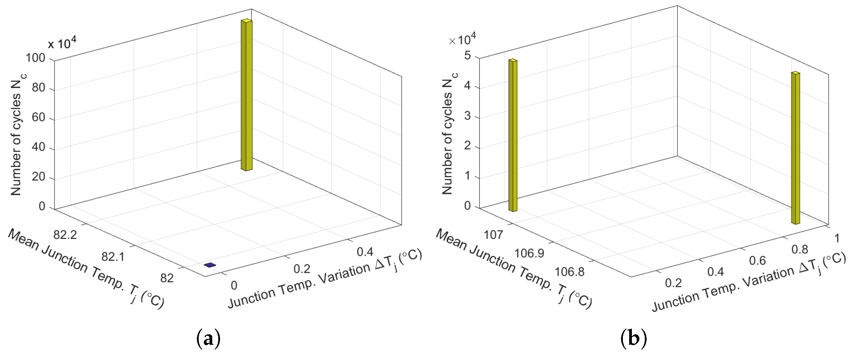
Figure 19.
Rainflow histogram of cycle counting considering the average junction temperature and the junction temperature variation : (a) for a load profile R = 13.1 ; (b) for a load profile R = 13.8 .
Figure 19.
Rainflow histogram of cycle counting considering the average junction temperature and the junction temperature variation : (a) for a load profile R = 13.1 ; (b) for a load profile R = 13.8 .

Figure 20.
Rainflow histogram of cycle counting considering the average junction temperature and the junction temperature variation : (a) for a load profile R = 15.2 ; (b) for a load profile R = 20 .
Figure 20.
Rainflow histogram of cycle counting considering the average junction temperature and the junction temperature variation : (a) for a load profile R = 15.2 ; (b) for a load profile R = 20 .


Table 1.
MOSFET Foster network: thermal resistance (K/W), capacitance (Ws/K), and time constant (s).
Table 1.
MOSFET Foster network: thermal resistance (K/W), capacitance (Ws/K), and time constant (s).
| Thermal Resistance | |||
| 0.2525 | 0.18024 | 0.0342 | 0.1976 |
| Thermal Capacitance | |||
| 0.42068 | 0.05191 | 0.001285 | 0.006952 |
| Time Constant | |||
| 0.10623 | 9.357 × | 4.3948 × | 1.374 × |
Table 2.
Accumulated fatigue results for the six load mission profiles.
| Load Mission Profile R | Number of Cycles | Number of Cycles | Accumulated Damage Q | Remaining Lifetime |
|---|---|---|---|---|
| 6 | 4.7158 × | 8.5 × | 0.0018% | 99.9982% |
| 8 | 3.14813 × | 4 × | 0.0021% | 99.9979% |
| 13.1 | 2.3953 × | 2466 | 1.029% | 98.971% |
| 13.8 | 8.1376 × | 4949 | 6.082% | 93.918% |
| 15.2 | 1.8654 × | 1887 | 10.116% | 89.894% |
| 20 | 2985.8 | 1956 | 65.53% | 34.47% |
Disclaimer/Publisher’s Note: The statements, opinions and data contained in all publications are solely those of the individual author(s) and contributor(s) and not of MDPI and/or the editor(s). MDPI and/or the editor(s) disclaim responsibility for any injury to people or property resulting from any ideas, methods, instructions or products referred to in the content. |
© 2024 by the authors. Licensee MDPI, Basel, Switzerland. This article is an open access article distributed under the terms and conditions of the Creative Commons Attribution (CC BY) license (https://creativecommons.org/licenses/by/4.0/).
Share and Cite
MDPI and ACS Style
Morel, C.; Morel, J.-Y. Impact of Chaos on MOSFET Thermal Stress and Lifetime. Electronics 2024, 13, 1649. https://doi.org/10.3390/electronics13091649
AMA Style
Morel C, Morel J-Y. Impact of Chaos on MOSFET Thermal Stress and Lifetime. Electronics. 2024; 13(9):1649. https://doi.org/10.3390/electronics13091649
Chicago/Turabian StyleMorel, Cristina, and Jean-Yves Morel. 2024. "Impact of Chaos on MOSFET Thermal Stress and Lifetime" Electronics 13, no. 9: 1649. https://doi.org/10.3390/electronics13091649
Note that from the first issue of 2016, this journal uses article numbers instead of page numbers. See further details here.