
Field Plate Integration for Mitigating Partial Discharge Activity in PCB-Embedded Power Electronic Modules

1
Université Grenoble Alpes, CNRS, Grenoble INP, G2Elab, 38000 Grenoble, France
2
Universite Claude Bernard Lyon 1, INSA Lyon, CNRS, Ecole Centrale de Lyon, Ampère, UMR5005, 69130 Ecully, France
*
Author to whom correspondence should be addressed.
Energies 2024, 17(9), 2035; https://doi.org/10.3390/en17092035
Submission received: 31 March 2024
/
Revised: 20 April 2024
/
Accepted: 23 April 2024
/
Published: 25 April 2024
(This article belongs to the Special Issue Energy, Electrical and Power Engineering 2024)
Abstract
:This paper proposes a concept based on field plate (FP) integration inside printed circuit board (PCB)-embedded power modules. The goal is to reduce the electric field at their surface and thus increase the partial discharge inception voltage (PDIV). Electrostatic simulations are first carried out to analyze the electric field reduction induced by the use of FPs. Then, dedicated experiments are proposed to demonstrate that the actual PDIV increases in AC sinus 50 Hz when FPs are implemented. More specifically, it is observed that an optimal FP length exists. Several analyses based on simulations and experiments are thus proposed to explain this phenomenon. Finally, an assessment of PD activity and PD location is presented to support the analysis. AC sinus 50 Hz characterizations indicate that PDIV can be increased by 178% compared to PCBs without FPs with a proper definition of equipotential prolongation and PCB length.
1. Introduction
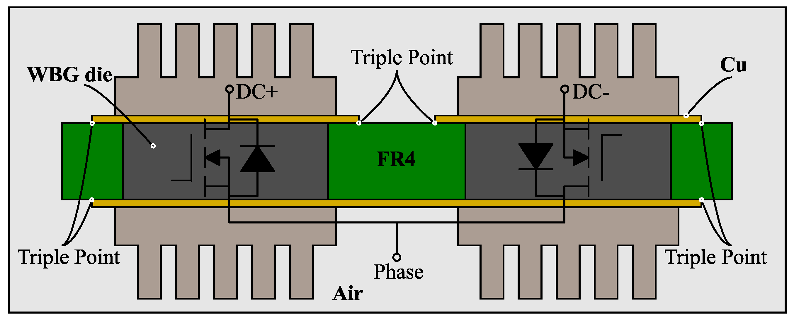
Currently, many power electronic developments focus on high−power density converters with massive integration of wide band-gap (WBG) semiconductors. Indeed, the management of high switching speed combined with higher efficiency and compacity leads researchers to find better integration solutions than the classical two-dimensional (2D) power module architecture [1]. Solutions based on three-dimensional (3D) structures and printed circuit boards (PCBs) with embedded dies allow for alleviating 2D weaknesses by reducing the stray inductance of switching loops [2]. Also, they make it possible to cool the dies on both sides [3]. For instance, Figure 1 presents a structure with a PCB-embedded switching cell made of two flip-chipped WBG dies, leading to a massive inductance loop reduction, as described in [4]. In this figure, the cooling is achieved by heatsinks attached to DC+, DC−, and phase electrodes. This solution allows for a possible gain in power density of the global converter [3]. Another advantage lies in the heatsink assembly on PCBs without thermal interface material (TIM), which allows for a decrease in thermal resistances [3].
Despite the advantages of this assembly from electrical and thermal points of view, some limits need to be considered. In fact, as referred to in Figure 1, several electrical triple points are present with possible high electric fields in these air areas. These geometrical singularities, largely studied in the literature [5], induce a clear voltage withstand issue—i.e., presence of partial discharges (PDs) and possible breakdown voltage (BDV)—that needs to be considered during the electrical design phase.
The literature presents several techniques to manage the electric field reinforcement at the triple point [6]. For instance, Waltrich et al. [7] propose applying a dielectric coating to reduce the electric field at this location. Other solutions lie in geometric modifications: Reynes et al. [8] propose modifying the shape of the metallization (i.e., sharp to round edge), and Hourdequin et al. [9] present a structure with a gap between two surface metallizations to improve electric field distribution. Although these techniques have proved their abilities, a supplementary manufacturing process is necessary in the case of material modification, while surface geometric modifications like in [8,9] seem to be more complicated for PCB applications compared to bulk materials classically used in 2D power modules.
A solution developed in [10,11] for high-voltage DC-link busbars lies in modifying the electric field configuration thanks to a capacitive field grading inside the PCB structure, with the advantage of a classical PCB manufacturing process. With this technique, the electric field reinforcement originally located at the triple point is reduced and transferred to another material with better dielectric rigidity than air, i.e., FR4 resin.
However, in the case of capacitive field grading dedicated to DC-link busbar applications, the studies are mainly focused on electric field management at the surface of the PCB. For instance, Cairnie et al. [11] depict the electric field management of PCB busbars in the air with high voltage potentials at the surface of the PCB. Ravi et al. [10] also study the electric field at the PCB surface with plated through hole (PTH), which connects both metallizations of PCBs. These different works are therefore not fully adapted to the assembly described in Figure 1 with a supplementary blocking voltage zone applied across the thickness of the PCB.
The present paper aims to study capacitive field grading structures, i.e., field plate (FP) designs, dedicated to PCB embedding assemblies, as shown in Figure 1, with a voltage applied across the thickness of the PCB. For this study, it is assumed that the off-state of the power chips is well managed, meaning that the voltage drop is fully transferred to the PCB. For a given applied voltage, the electric field mapping inside (FR4) and outside (Air) the PCB will be determined solely by its design. Figure 2a depicts a possible PCB architecture inspired by the capacitive field grading method adapted to PCB embedding assemblies. The dashed rectangle represents the area concerning the present work and is zoomed in Figure 2b with the representation of horizontal and vertical surfaces of the PCB. Note that the power chips in Figure 2a are not considered in this study, and TOP and BOT FPs are only studied in a symmetrical configuration as a result of previous works [12].
The creepage design rules for PCBs have shown their limits, specifically with the use of WBG devices and the need for PD-free setups for lifetime purposes. An innovative design method was presented in [13,14] based on three steps: (i) stress profile calculation (simulation); (ii) intrinsic aging and discharge modeling; and (iii) validation of the PDIV estimation and inherent discharge model through PDIV measurements. A very good understanding of the PD location (with an accurate geometrical description) is needed to be able to perform the second step, i.e., the discharge modeling. For the present study, the first step is kept to identify the electric field reinforcement areas, and the third step (PD activity and location) is used to compare the performances of different setups.
The next section presents a preliminary study of the concept based on numerical simulations. Both geometries, without and with FPs, are firstly simulated to highlight the shifting of the maximum electric field induced by the FPs disposition. Then, a parametric study aims to analyze the decrease trends brought by the FP concept and to select the most interesting PCB configurations to be characterized. Then, this paper continues with the presentation of different PCB assemblies and the experimental setup dedicated to PD activity assessment. PD experimental results in AC sinus 50 Hz are presented with partial discharge inception voltage (PDIV) characterization, PD activity evaluation, and analysis of PD location.
2. Preliminary Study of the Concept Based on Numerical Simulations
This section compares different PCB geometries representative of the assembly of Figure 2b, with and without a capacitive field grading structure. The objectives of these simulations are (i) to identify the weaknesses areas based on an electric field reinforcement analysis and (ii) conduct a parametric study to evaluate the impact of different PCB design parameters on the maximum electric field. This study is based on finite element numerical simulations developed with COMSOL Multiphysics V6.0 software and electrostatic physics resolution. The reference case, i.e., without FPs, is studied in the next subsection. Then, configurations with FPs are evaluated in the second subsection.
2.1. Reference Case: PCB without Field Plates
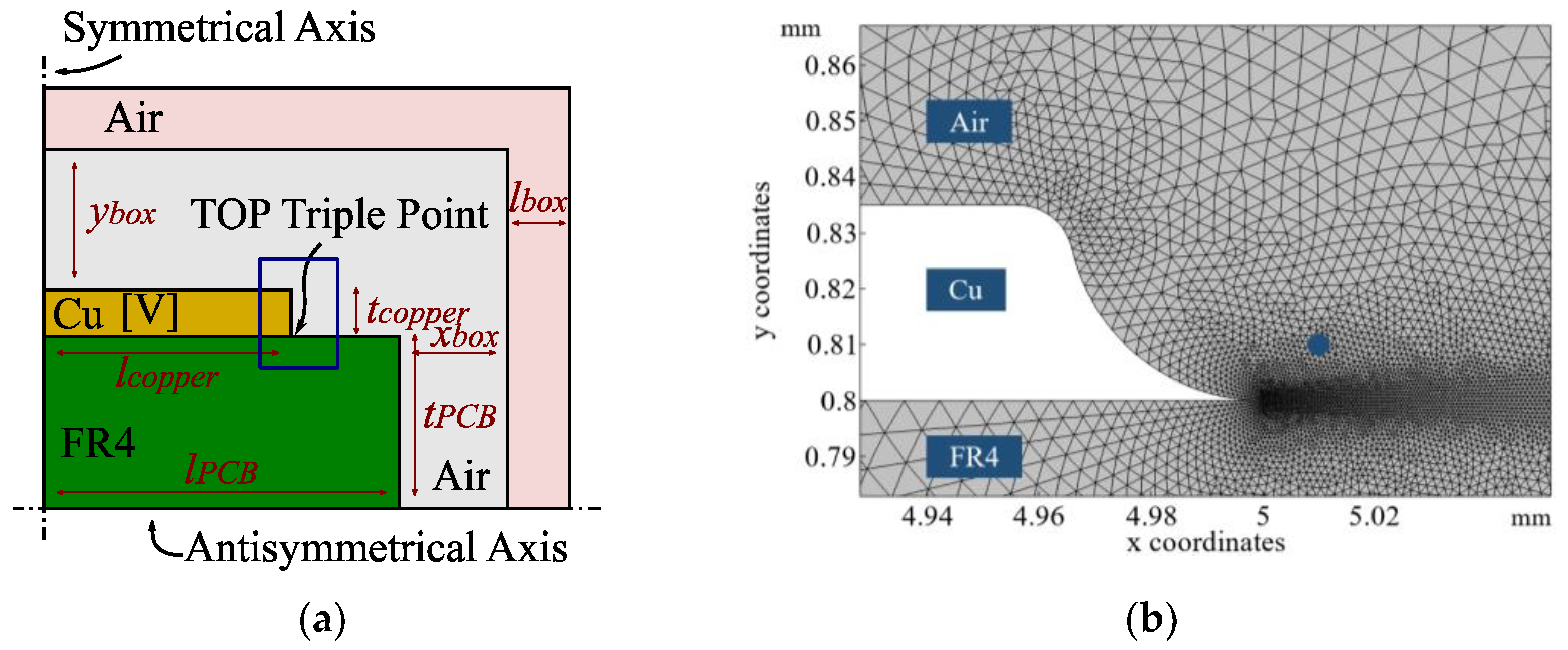
A schematic pattern of the reference case without embedded dies is shown in Figure 3a with geometrical parameters representative of the desired application. A 2D geometry is simulated with two different symmetries. A y-axis symmetry plane and an x-axis anti-symmetrical plane allow for simulating a quarter of the PCBs geometry. All geometrical dimensions are summarized in Table 1. For the electric field calculation, assuming no space charges in the dielectric medium, the Poisson equation can accordingly be reduced to a Laplace equation.
For the boundary conditions, an infinite box is mandatory to represent the air domain around the PCB. The copper plate potential is set at 5 kV. Outer boundaries of this domain, defined far enough from the potentials (xbox and ybox parameters), are defined as Dirichlet boundary conditions where inductive field is set to zero. Symmetry planes of the y and x axes are, respectively, defined to symmetry (a null normal component of field) and anti-symmetry (a null tangential component of field defined to 2.5 kV, i.e., half of the high voltage potential).
The presence of three materials with different permittivities in the simulated geometry entails considering some numerical simulation limitations due to the triple point effect [15]. Therefore, the shape of the edges of the metallizations are modified for carrying out electrostatic simulations and the mesh is accordingly refined around the triple point (Figure 3b). Moreover, to bypass singularities of numerical calculations, the electric field is measured at 14 µm (point A represented in Figure 3b) from the triple point, as suggested by [15]. Therefore, all electric field values, named Efield, linked to the triple point will refer to point A for the rest of this article.
Figure 4 shows simulation results and represents equipotential lines and electric field mapping in the air and FR4 without FPs. With Efield at point A equal to 11.4 kV/mm, the air volume near the copper edge metallization is clearly identified as a weak point, potentially leading to voltage breakdown or partial discharge activity.
Given that voltage withstand issues can lead to the destruction of power modules, solutions must be proposed to guarantee that the maximum electric field is lower than the dielectric rigidity of the weakest material, i.e., the air. The next section thus presents an evaluation of the impact of FPs on reducing this electric field.
2.2. Impact of Field Plates on Electric Field Map
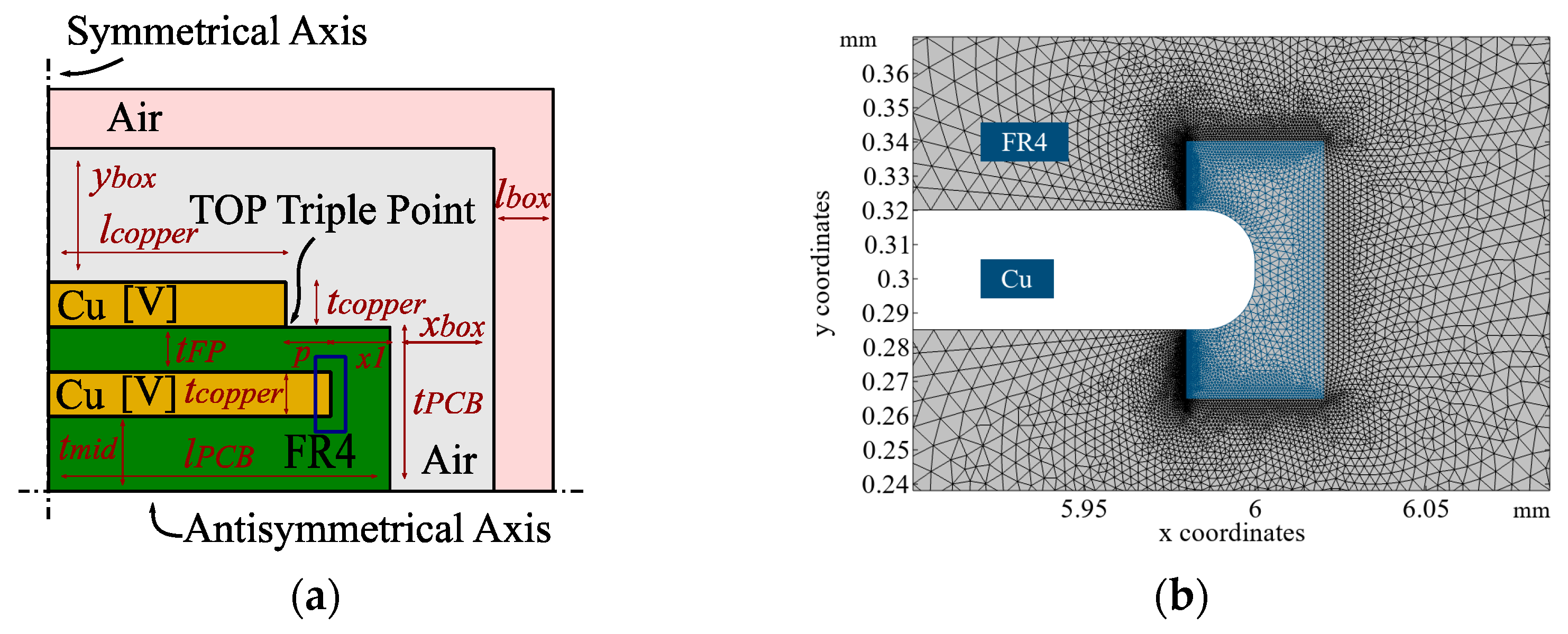
Previous numerical simulations on different FP configurations, not detailed in this paper [12], have shown that the best FP pattern is achieved with a symmetrical configuration of the FPs (Figure 2b) inside the PCB. Thus, only this configuration is studied in the present work. Figure 5a represents the schematic pattern of a PCB with FPs, with all geometrical dimensions summarized in Table 1. This multilayer PCB is made up of two conductive layers. The first one (outer layer) has the same location and dimensions as the reference case without FPs. The second one (inner layer acting as FP) has a larger width, with p being the offset between outer and inner layers and referred to as the equipotential prolongation. The electric potential of both copper conductive layers is set at 5 kV. The boundary conditions are the same as the ones used in the previous paragraph.
2.2.1. Simulation Results—General Trends
The simulation results of the PCB with symmetrical FPs (p = 1 mm) are illustrated in Figure 6. A comparison of the electric field maps of Figure 4 and Figure 6 highlights the effect of the capacitive field grading concept with the transfer of the maximum Efield from the triple point to the FP edge. The 1.14 kV/mm Efield at point A represents a decrease of 90% compared to the reference case.
Nevertheless, the presence of inner layers lies in an electric field reinforcement at the end of the FP, leading to (i) a possible PD inception inside the FR4 resin as a result of micro air cavities, and (ii) a possible BDV through the FR4 resin. This reinforcement is evaluated with the measurement of the maximum electric field inside a defined area represented by the rectangle of Figure 5b. A maximum electric field of 29.4 kV/mm can be evaluated in this zone with p = 1 mm. This value represents an increase of 158% compared to the 11.4 kV/mm maximum electric field in the reference case (Figure 4). The electric field decrease observed at the triple point is consequently balanced by an increase inside the FR4. Considering that the theoretical dielectric rigidity of air is much lower than that of FR4, this Efield reinforcement at the edge of the FP is considered a consequence and not a problem of the concept.
2.2.2. Parametric Analysis of Electric Field around PCBs with FPs
The previous simulations have clearly demonstrated the advantage of the capacitive field grading concept and the electric field decrease at the triple point. However, targeting the definition of design rules and the reduction in power module volume, a parametric study is performed to better circumscribe the field plate effect. The first part of the parametric study proposes analyzing the influence of the equipotential prolongation p for a fixed PCB length. Then, the second part proposes studying the effect of the PCBs length lPCB for a fixed p value.
For the analysis, different measurement lines are defined along the PCB geometry. These lines, represented in Figure 7, are called the horizontal line (H) and vertical line (V), while point A represents the location of Efield measurement at the triple point like in the previous subsection. Note that point A is included in the H line.
Figure 8a represents maximum Efield values in the different measurement areas with lPCB = 10 mm and p in the range of 0 mm to 4.9 mm. With p = 0 mm, the Efield at point A is 7.0 kV/mm, which represents a 39% decrease compared to the reference case without FPs. The analysis of simulation results indicates that, as p increases, the Efield value at point A decreases exponentially. Thanks to the FPs, a 98% decrease can be observed with p = 4.9 mm.
An analysis of the maximum electric field along the horizontal line H of the PCB indicates two distinct trends as p increases. With p in the range from 0 mm to 0.7 mm, the result follows the same trend as the triple point, with identical maximum Efield values. This means that the maximum Efield remains close to the triple point since point A is included in the H line. When p is greater than 0.8 mm, the maximum Efield value is constant and equal to 1.8 kV/mm until p = 3.5 mm. Also, Figure 8a shows that, with equipotential prolongations above 4.2 mm, the maximum Efield in the air shifts from the H line to the V line due to the proximity of the FPs edge to the air domain at the PCB edge. This increase is strongly dependent on the p parameter since the maximum Efield values along V of 2.0 kV/mm and 7.7 kV/mm are obtained when p equals, respectively, 4.3 mm and 4.9 mm.
The first part of the parametric study underlines the major advantage of capacitive field grading concept with the decrease in Efield in the air as p increases, except if the FP and PCB edges are too close to each other. To confirm that, another parametric study aims to study the impact of lPCB on maximum Efield value and location for a fixed equipotential prolongation. Figure 8b summarizes the results of this study with p = 1 mm and lPCB between 6.5 mm and 10 mm. The analysis of simulation results indicates that as lPCB increases, the Efield value at point A is quasi-constant and close to 1.1 kV/mm. This result indicates a decrease of 90% compared to the reference case without FPs and validates the equipotential prolongation benefit. An analysis of the Efield along the V line indicates that with the lPCB parameter in the range of 6.5 mm to 6.8 mm, the maximum Efield is located on the vertical surface of the PCB. This comment supports the influence of the PCB edge on maximum Efield location as a result of the close proximity of FP edges. Finally, for lPCB greater than 7.5 mm, the maximum Efield is equal to 1.8 kV/mm and located on the H line. This constant Efield value indicates a possible gain on the PCB surface with no influence of the lPCB parameter on the maximum Efield value and location.
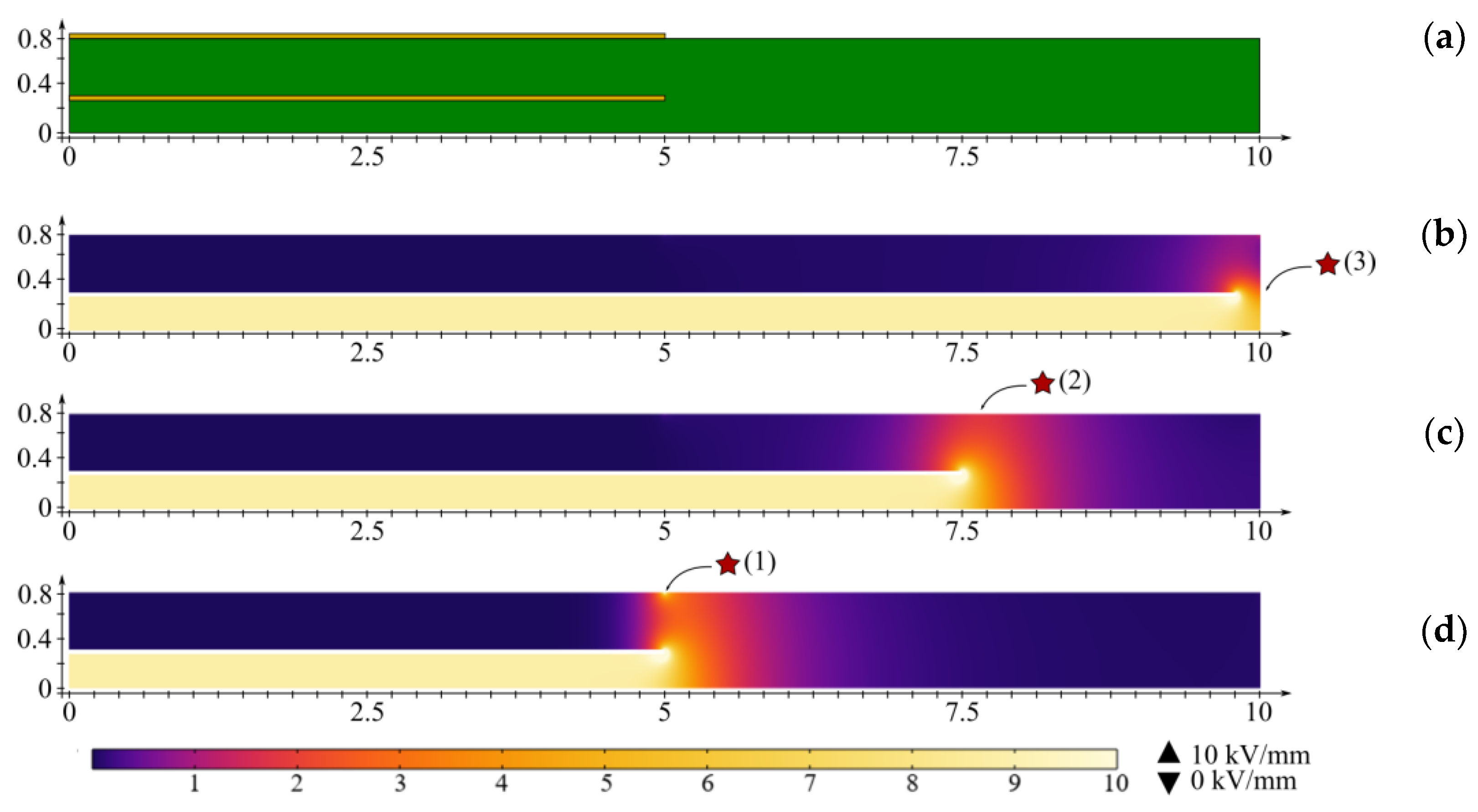
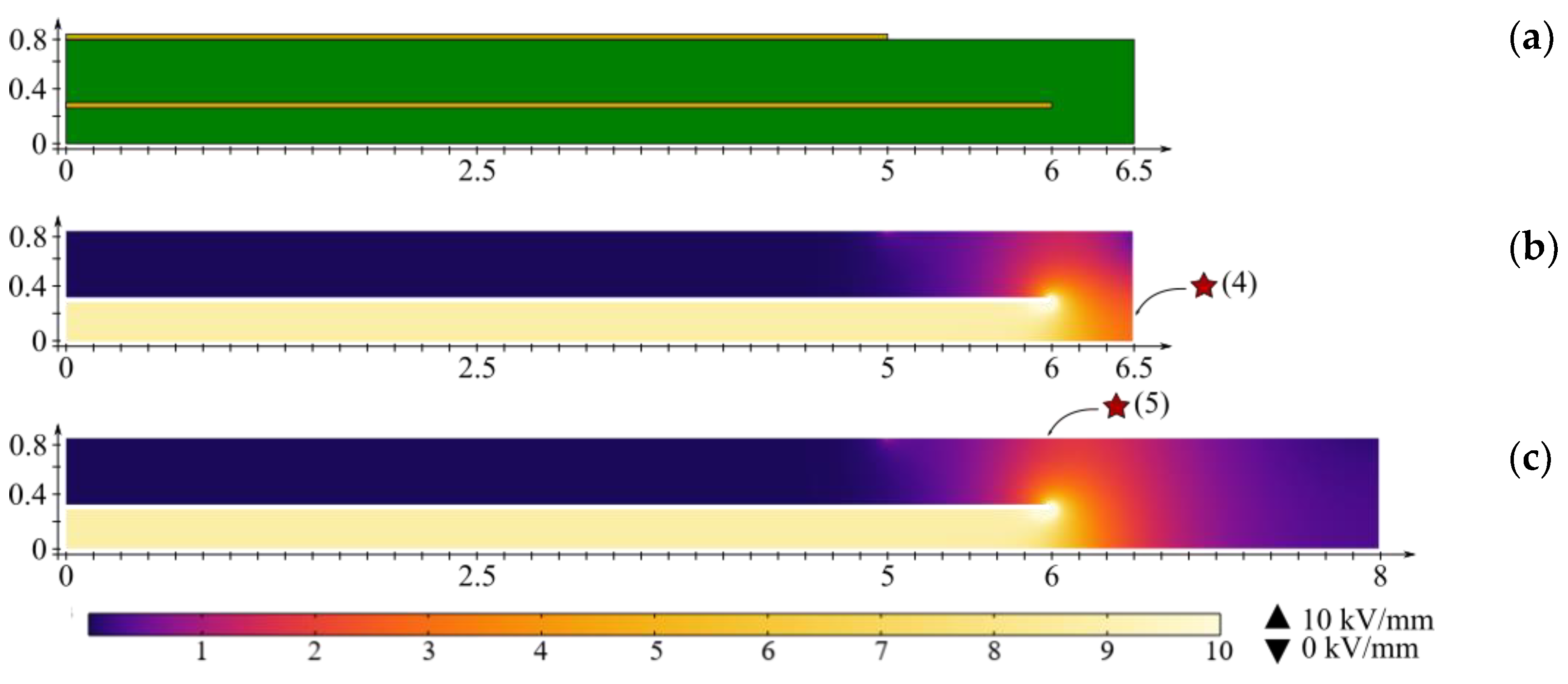
To better illustrate the shift in the maximum Efield in the air, the electric field map of markers (1), (2), and (3) of Figure 8a are, respectively, represented in Figure 9b, Figure 9c, and Figure 9d for variations in the equipotential prolongation p. The displacement of the maximum Efield of markers (4) and (5) from Figure 8b are, respectively, represented in Figure 10b and Figure 10c. These Efield maps allow for us to clearly observe the displacement of the maximum Efield from point A to the H line with an increase in p from 0 mm to 2.5 mm and a displacement from the H to V line with p = 4.9 mm. The influence of the PCB edge is also shown in Figure 10b,c for lower PCB lengths. Accordingly, it is therefore possible to underline that the FP design must be conceived considering not only the equipotential prolongation, but also the distance between the FP and PCB edges. This last parameter is referred as x1 in Figure 5a and will be used in the next section.
The parametric study demonstrates the advantages of a PCB with FPs from a design point of view.
Table 2 summarizes the different interesting cases highlighted by the various simulation results. Based on the equipotential prolongation study, i.e., cases 1 to 3, a global decrease in the maximum Efield for each PCBs geometry can be underlined with differences between −32% and −84% compared to the PCB without FPs, i.e., case 0. Among all these improvements, case 2 seems to be the most interesting geometry, with maximum Efield reduction.
With variations in PCB length, the objective is to study the possibility of decreasing the PCB surface, keeping in mind that power density represents an important criterion in power modules [16,17]. By this way, cases 4 and 5 also allow for decreases of 73% and 84%, respectively, compared to the PCB without FPs. An interesting comparison lies between cases 2 and 5 with the same maximum Efield in the H line and different PCB lengths. With this last change, a decrease of 2 mm in PCB length is possible and therefore highlights the possibility of increasing power density with a decrease in the Efield value at the triple point.
3. Impact of Field Plates on Partial Discharge Inception Voltage
3.1. PCB Design and Test Vessel
This experimental study aims to focus on the effect of field plate geometry on PCB partial discharge (PD) behavior. For comparison purposes, different configurations were made for the tests (Figure 11). They all included two 10 mm × 40 mm × 35 µm metallizations on their external sides. Design A is defined as the reference case without FPs. Three other designs (B, C, and D) included FPs with the same PCB size and the aim was to study the FP length impact on PDIV values. Finally, the two last designs (E and F) were used to study the influence of the lPCB parameter with the same FP surface as design C but with a reduction in PCB size. All geometrical dimensions are given in Table 3, where tFP and tmid represent the FP depth and distance between FPs, respectively. In design B, the inner and outer copper layers have the same area. In designs C, E, and F, the offset between outer and inner layers is p = 2.5 mm. Finally, design D maximizes the FP equipotential prolongation with p = 4 mm. Five specimens were fabricated and characterized to carry out a statistical study of the results by design. The volume of the different samples was 20 mm × 50 mm × 1.6 mm for designs A, B, C, and D; 16 mm × 46 mm × 1.6 mm for design E; and 17 mm × 47 mm × 1.6 mm for design F.
Figure 12a represents the experimental test vessel for PD characterization. The PCB is inserted between two 12.5 mm diameter spherical electrodes connected to high-voltage and ground potentials, respectively. PD measurements were performed with an AC sinus 50 Hz voltage in compliance with IEC 60270 standard recommendations using an Omicron commercial system. The setup has been used in the research group’s previous works, like in [18], and is represented in Figure 12b. For the PDIV measurement, each sample was submitted to a slow 0.4 kV/s linearly increasing voltage until the PDIV was reached, with a 10 pC threshold. To avoid PDs due to sample preparation instead of geometrical influence, a few pre-conditioning tests were performed. The average of the last five results was accordingly considered as the PDIV of the sample.
3.2. AC Sinus 50 Hz PDIV Experimental Results
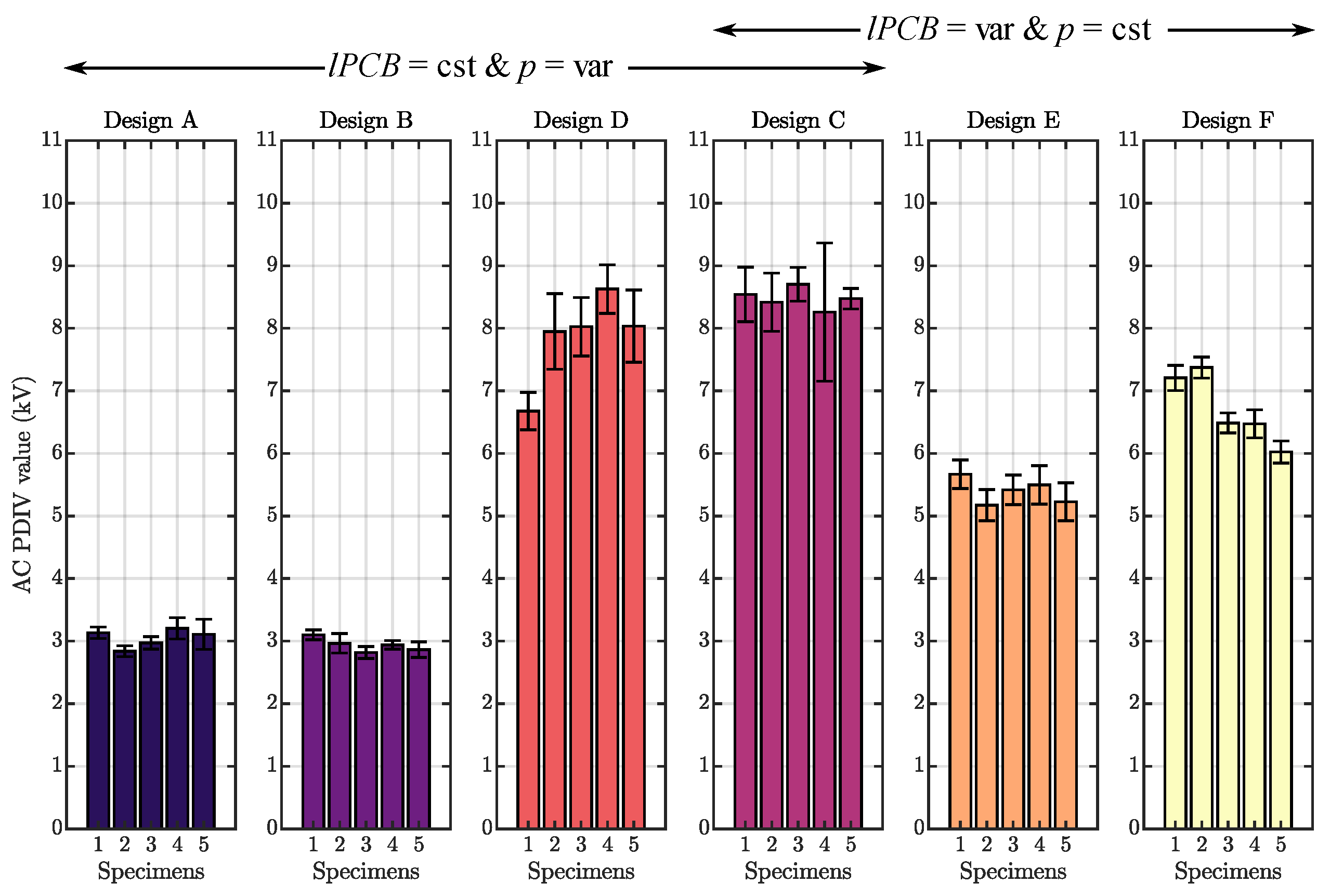
Figure 13 depicts the mean PDIV values of the five specimens of each configuration with associated standard deviations. The maximum and minimum PDIVs with the associated standard deviations of each design are summarized in Table 4. The table also gives the maximum deviation (ΔPDIV), which is the difference between the maximum and the minimum PDIV of each design. Due to the relative uniformity of the results per design, the global average of all designs (mean of the five specimens) was computed. The results are summarized in Figure 14a, and Table 5 provides some inputs on the influence of the p parameter on the PDIV. With a difference of −3.61% for design B compared to the reference case, the capacitive field grading effect is limited with p equals to 0 mm, contrary to what was observed in the electric field simulations. The other configurations give increases of +178%, +158%, +77%, and +120%, respectively, for designs C, D, E, and F. These increases are facilitated by the FP equipotential prolongation and confirm the trend observed in the simulation with a high reduction of the electric field in the air. Conditions for the inception of PD events are therefore rejected to higher voltage values.
To link the simulation and experimental works, the PDIV results were also analyzed based on the x1 parameter (distance inside the PCB between the FP and the PCB edges) and are depicted in Figure 14b. The results indicate a global increase in PDIV values as x1 increases with, for example, +57% in design C compared to design E with a fivefold increase in x1. Taking design E as a reference (with the smallest x1), the relative increase in PDIV for the other design is given in Table 6. Interesting behavior lies in the comparison of designs F and D with equal board edge distances, x1 = 1 mm. Indeed, despite the same design in x1, the PDIV results of designs F and D are, respectively, equal to 6.71 kV and 7.86 kV, i.e., a +17% increase for the latter. This observation does not match with the parametric study carried out in the numerical simulation, where the independent behavior of the Efield resulted as PCB length increase was obtained for a constant equipotential prolongation. This comment can underline a possible weakness of the electric field simulation as design criteria with an incomplete representativeness of real physical phenomena. This is particularly true for pre-breakdown or breakdown phenomena and therefore for partial discharge activity.
Finally, a global increase in PDIV results was obtained with an increase between +77% and +158% for the p parameter ranging from 2.5 mm to 4 mm. However, this increase needs to be counterbalanced by the geometry of the PCB edge characterized by x1. Despite a global increase with p, a proper selection of x1 allows for better enhancing PDIV results with an increased range from +77% to +178%, due to a good balance between the FP equipotential prolongation and the board edge influence. To conclude, the PDIV characterization underlines the advantages of the capacitive field grading concept.
However, PDIV is not the only information of interest for PD characterization; an important aspect lies in the PD activity of the different PCB designs when PD activity is maintained on time. The next section aims to study the PD activity of all configurations.
4. Experimental Characterization of AC Sinus 50 Hz PD Activity
The objective of this section is to compare and analyze the PD activity of each configuration of Figure 11. The same specimens as in the previous section were used. PD activity was characterized with a defined protocol, represented in Figure 15. AC sinus voltage was linearly increased at 0.4 kV/s until it reached a plateau, defined as 110% of the calculated PDIV. The 10% margin above the PDIV value guaranteed a clear evaluation of PD activity on each tested sample. This voltage was maintained for 30 s in order to record data. The RMS voltage was finally decreased at the same slope as the increasing one. This protocol was repeated five times for each sample in order to deduce the following average values:
- The maximum charge Qmax during PD activity characterization;
- The average charge Qavg during PD activity characterization;
- The number of PD events per second N during PD activity characterization;
- The partial discharge extinction voltage (PDEV), which represents the voltage value when PD events lower than a defined threshold, i.e., 10 pC, were measured.
Figure 16a represents the phase-resolved partial discharge (PRPD) patterns of sample 1 from design A. As can be seen, a background noise band around ±10 pC is measured and interpreted as PD activity during the measurement if not removed. Without any PD activity, the background noise of the setup is about ±300 fC, but due to the automatic gain adaptation of the Omicron setup, this background noise is increased when PD events of strong magnitude are measured. As these results may distort some quantities like N and Qavg, all PD events lower than the noise level are deleted before computing the quantities.
Example of PRPD pattern for designs A, B, and E are, respectively, represented in Figure 16b, Figure 16c, and Figure 16d. As can be observed, PDs mainly occur in the first and third quadrants of the voltage phase. With a PD activity maintained on time, PD events can occur at voltage values lower than the maximum one, even close to zero, due to the presence of space charges at the surface of the PCB [19]. The phase of the PD events confirms the presence of surface PDs on tested samples, i.e., PD in the air and not in the volume of the PCB [19,20]. The symmetrical PRPD signature between positive and negative half-cycles is due to the symmetrical structure of the test samples.
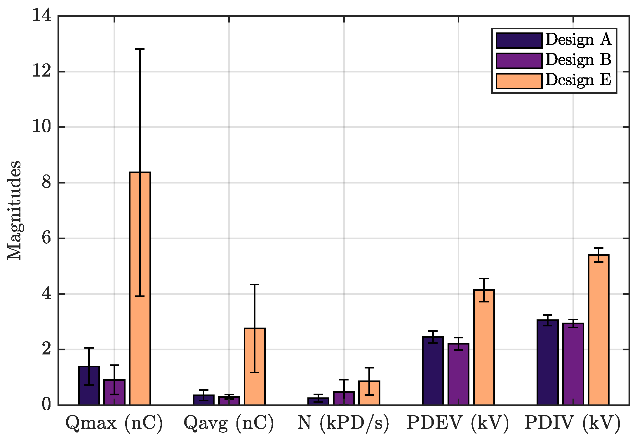
To enable comparison of PD activity, the overall mean values with the standard deviations (five patterns of five specimens per configuration) of all quantities are summarized in Figure 17 for designs A, B, and E. Note that the PD activity characterization is not possible for designs C, D, and F. Indeed, due to the effect of the FPs, respective PDIVs are too close to the BDV and thus some BDV events are observed during PDIV characterization for these configurations. Table 7 summarizes the mean values of all the quantities and are systematically compared to design A, which is taken as the reference. It can be noticed that in terms of Qmax and Qavg, design B exhibits a lower PD activity but with a higher N. A small decrease in the PDIV is observed for design B. With a factor of 6, 7.8, and 3.42 in, respectively, Qmax, Qavg, and N compared to the reference design A, design E exhibits much higher PD activity but also with a 1.77-times higher PDIV, meaning that the tests on this design are performed with a voltage nearly 2 times higher. With the ratio between PDIV and PDEV, respectively, equal to 1.24, 1.33, and 1.30 for designs A, B, and E, the conditions of the PD extinction are similar for all the designs. Finally, the previous results and the general trends observed in Figure 17 underline the specific behavior of design E compared to designs A and B.
The experimental characterization of PD activity of each configuration allows for us to gain a deeper understanding of the PD behavior of PCBs with FPs. Some preliminary results can be pronounced:
- The small differences between the PDIV results of samples A and B are confirmed in terms of PD activity, highlighting the limited impact of multilayer PCBs if the FPs do not ensure an equipotential prolongation.
- When the PDIV is reached, the PD activity of design E is clearly higher than those of designs A and B. This higher PD activity and the fact that the other designs with FPs—i.e., designs C, D, and F—are often subjected to breakdown for voltages reaching 110% of the PDIV reveal that FPs with equipotential prolongation improve the PDIV but reduce the margin between PDIV and breakdown.
5. Optical Characterization of Partial Discharge Localization
Previous PDIV characterizations of PCBs without and with FPs allowed for us to demonstrate the impact of equipotential prolongation p with an increase in PDIV values. The objective of this section is to experimentally verify the localization of PD events for different PCB configurations and compare with the simulation study.
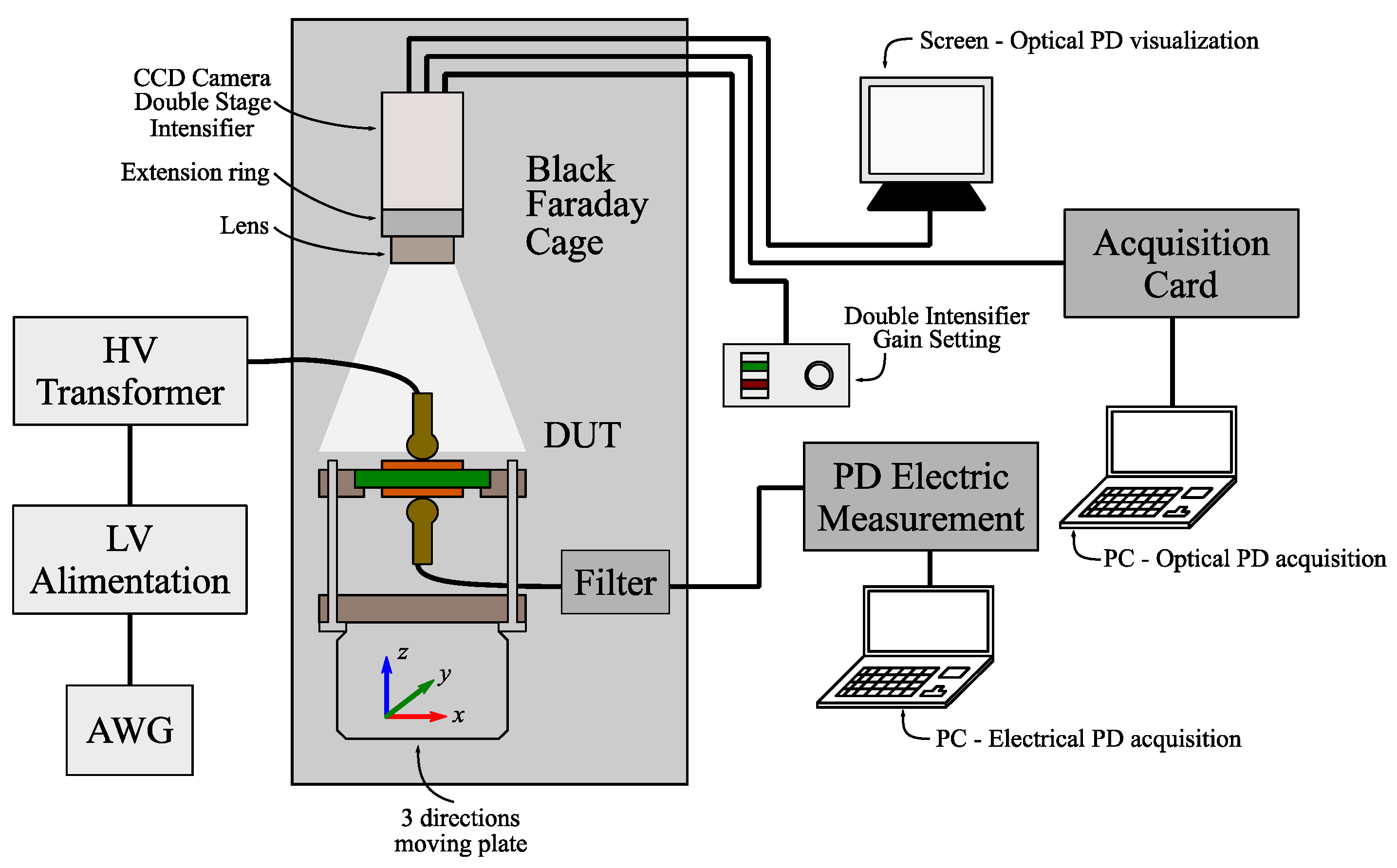
The characterization of PD localization is based on an optical measurement in a dark enclosure [21,22], which makes it possible to visualize the photons emitted by PD events. The experimental test bench used for this characterization is depicted in Figure 18. Optical visualization was carried out thanks to a high-sensitivity camera constituted by a charge-coupled device (CCD) image sensor coupled to a double-stage image intensifier. This type of measurement is well suited to the tested vehicles developed in this article since the dielectric domain, i.e., the air, is transparent and the PD events are located at the PCB surface. Additionally, the epoxy resin used in the PCB manufacturing process is not electroluminescent. An acquisition card allowed for registering pictures from the CCD camera and a dedicated screen allowed for online PD visualization. A more detailed description of the test bench in Figure 18 is given in [22]. Classical electrical PD measurement can be performed at the same time to visualize the PRPD pattern.
Only one face of the device under test (DUT) can be visualized with the CCD camera, i.e., only PD events on the upper surface of the PCB can be observed. As the objective of this characterization is to compare with simulation results, a symmetrical configuration of the electric field is mandatory, with a sufficient air domain near the ground electrode. Each PCB was therefore mounted on a plastic frame to connect to the lower electrode.
The first step of the characterization aimed to set the focus, with a little amount of light, of the CCD camera by setting the gain of the double-stage intensifier and the quality of the lens. Figure 19a depicts a typical result of this focus part with a clear dissociation of the different areas of the DUT. The red lines represent the PCB corners while the dashed blue ones represent the corners of the outer metallization. Note that the white part of Figure 19a represents the HV wire used for the connection of the HV transformer output to the DUT. It is visible when carrying out the focusing but is not visible during PD tests, which are performed in a totally dark environment.
The second step of the characterization aimed to visualize the PD events with the CCD camera and conclude the PD localization. For that, the AC sinus 50 Hz RMS voltage value was increased until PD events were measured with the PD electric measurement system. When PD state was reached and PD events were visualized with the online screen, a picture could be registered. The registered picture represents the average of five consecutive measurements to reduce the intrinsic noise of the camera. Figure 19d allows for us to visualize the light spot emitted by the PD event at the surface of the reference sample without FPs.
The AC sinus 50 Hz PD localization characterization was carried out for one sample of designs A, B, and E. The other configurations, i.e., designs C, D, and F, were not tested due to the conclusion highlighted in the previous section that showed that the BDV and PDIV values were too close. Indeed, in the case of a BDV event on a tested sample, the light emitted by the plasma channel could saturate the double-stage intensifier and deteriorate the CCD camera. Experimental results of designs A, B, and E are, respectively, summarized in Figure 19d, Figure 19e, and Figure 19f. The associated focus results are depicted in Figure 19a–c. HVs applied to each sample of the presented results are summarized in Table 8 with the associated PD localization. With applied voltage higher than the global PDIV of each design, it can be confirmed that light spots on each picture are PD events.
With this setup, the PD localizations of each design were determined and compared to the results of the numerical simulations. For design A, a light spot is located at one corner of the outer metallization, which represents one triple point of the PCB geometry. This result is coherent with the numerical simulation results of Figure 4, where the maximum Efield is identified at point A. Figure 19e shows that, for design B, three different light spots are located in three corners, which all refer to triple points of the PCB geometry. Once again, this result is consistent with the simulation part where, despite the presence of FPs, a null equipotential prolongation induces a maximum Efield at point A. Finally, in design E, multiple light spots were identified on the edge of the PCB. This last result confirms the benefit of FP disposition inside the PCB with a clear shift in PDs, from the triple point to the PCB edge, as was observed in the simulation study with the maximum Efield on the V line like in case 3 or 4 of Table 2.
Despite the agreement between the maximum Efield location in the simulation and the PD experimental localization, it can be noticed that the right angles formed by the copper plates at the PCBs surface add supplementary singularities that induce higher Efield values and thus are an ideal place for the PDs appearance. This phenomenon shows the limitation of 2D simulations for those setups.
6. Conclusions
In this paper, the management of the electric fields of 3D power modules isolated with air was studied. More specifically, a capacitive field grading solution dedicated to PCB embedding technology was evaluated. The originality of the present work is in the study of the electric field repartition inside and outside the volume of the PCB, with the blocking voltage applied across its thickness.
Numerical simulation of different field plate configurations allowed for us to conclude on the attenuation of the electric field at the triple point thanks to equipotential prolongation p. This reduction was, however, counterbalanced by a shift in the maximum electric field in the air to other areas, i.e., on the horizontal or vertical surface of the PCB. This shifting was exposed with a parametric study of parameters like the equipotential prolongation and field plate edge distance x1 to the PCB edge. A proper definition of both design parameters allowed for reducing the maximum electric field compared to the PCB without field plates and maximized this reduction. Also, simulation results highlighted a possible gain in power density with a reduction in PCB size under constant field constraints.
From experimental characterizations, a global increase in PDIV with the presence of FPs was observed. With an equipotential prolongation p of 2.5 mm, an increase of 178% was observed compared to the PCB without FPs. With the decrease in PCB surface and the conservation of p = 2.5 mm, increases of 77% and 120% were observed. These last results also confirmed the benefits of equipotential prolongation and the influence of PCB edge distance with a decrease in PDIV values when parameter x1 is decreased.
An opportunity for future work includes exploring the possibility of a six-layer PCB with two FPs for HV and ground potentials, respectively. Cairnie et al. [23] studied this assembly for a busbar application with an optimization algorithm. In the future, the same type of assembly could be simulated and characterized in the case of a PCB-embedded power module with high voltage applied in the thickness of PCB.
While performing PD activity assessment thanks to a PRPD pattern analysis, it was observed that PDs always occur at the surface of the PCB. It was also observed that for designs with an effective equipotential FP prolongation, the margin between PDIV and breakdown was reduced. That means that FP increases PDIV, but the PD ignition Efield is close to the breakdown ignition Efield. This result will have to be considered while defining a design rule for PCBs with FPs.
Next, optical PD localization measurements were carried out. The displacement of PD events from triple points to the edge of the PCB was highlighted and this confirmed the displacement of electric field intensification zones observed with numerical simulations.
Despite all the advantages, some limits were underlined. Firstly, a 2D representation of the simulated geometry is too restrictive with the absence of some areas of electric field strengthening. This comment is supported by the optical localization measurement with PD events in the corners of the metallization that are not represented by 2D simulations. Secondly, while being aware that simulation of the Laplacian electric field cannot simulate all the electric stresses present on a PCB, a fairly good correlation between simulation and measurement was observed, particularly concerning the PD locations. Finally, future additional works aim to study and characterize this capacitive field grading concept with high dv/dt square voltage constraints to get as close as possible to real power electronic voltage constraints.
Author Contributions
Conceptualization, P.B., E.V. and Y.A.; methodology, P.B., E.V. and Y.A.; software, P.B.; validation, P.B., E.V. and Y.A.; investigation, P.B., E.V. and Y.A.; writing—original draft preparation, P.B.; writing—review and editing, P.B., E.V. and Y.A.; supervision, E.V. and Y.A.; project administration, Y.A.; funding acquisition, Y.A. All authors have read and agreed to the published version of the manuscript.
Funding
This research was funded by Region Auvergne-Rhônes-Alpes (TAPIR project—Pack Ambition Recherche 2021) and ANR agency (ANR-21-CE05-0037).
Data Availability Statement
The original contributions presented in this study are included in the article; further inquiries can be directed to the corresponding author.
Acknowledgments
The authors would like to personally thank Rachelle Hanna and Olivier Lesaint for their valuable help on the partial discharge localization experiments.
Conflicts of Interest
The authors declare no conflicts of interest.
References
- Mantooth, H.A.; Ang, S.S. Packaging Architectures for Silicon Carbide Power Electronic Modules. In Proceedings of the 2018 International Power Electronics Conference (IPEC-Niigata 2018-ECCE Asia), Niigata, Japan, 20–24 May 2018; pp. 153–156. [Google Scholar]
- Risch, R.; Biela, J. PCB-Embedded Packaging for Ultra-Fast Switching of SiC MOSFETs. In Proceedings of the CIPS 2022—12th International Conference on Integrated Power Electronics Systems, Berlin, Germany, 15–17 March 2022; pp. 1–7. [Google Scholar]
- Bikinga, W.-F.; Mezrag, B.; Avenas, Y.; Schanen, J.-L.; Guichon, J.-M.; Alkama, K.; Dupont, L.; Bley, V.; Vagnon, E. TAPIR (compacT and modulAr Power Modules with IntegRated Cooling) Technology: Goals and Challenges. In Proceedings of the 2021 Third International Symposium on 3D Power Electronics Integration and Manufacturing (3D-PEIM), Osaka, Japan, 21–23 June 2021; pp. 1–6. [Google Scholar]
- Domurat-Linde, A.; Hoene, E. Analysis and Reduction of Radiated EMI of Power Modules. In Proceedings of the 2012 7th International Conference on Integrated Power Electronics Systems (CIPS), Nuremberg, Germany, 6–8 March 2012. [Google Scholar]
- Wang, L.; Zeng, Z.; Sun, P.; Ai, S.; Zhang, J.; Wang, Y. Electric-Field-Dominated Partial Discharge in Medium Voltage SiC Power Module Packaging: Model, Mechanism, Reshaping, and Assessment. IEEE Trans. Power Electron. 2022, 37, 5422–5432. [Google Scholar] [CrossRef]
- Cairnie, M.; DiMarino, C. Review of Electric Field Reduction Methods for Medium-Voltage Power Modules. In Proceedings of the CIPS 2022—12th International Conference on Integrated Power Electronics Systems, Berlin, Germany, 15–17 March 2022; pp. 1–6. [Google Scholar]
- Waltrich, U.; Bayer, C.F.; Reger, M.; Meyer, A.; Tang, X.; Schletz, A. Enhancement of the Partial Discharge Inception Voltage of Ceramic Substrates for Power Modules by Trench Coating. In Proceedings of the 2016 International Conference on Electronics Packaging (ICEP), Hokkaido, Japan, 20–22 April 2016; pp. 536–541. [Google Scholar]
- Reynes, H.; Buttay, C.; Morel, H. Protruding Ceramic Substrates for High Voltage Packaging of Wide Bandgap Semiconductors. In Proceedings of the 2017 IEEE 5th Workshop on Wide Bandgap Power Devices and Applications (WiPDA), Albuquerque, NM, USA, 30 October–1 November 2017; pp. 404–410. [Google Scholar]
- Hourdequin, H.; Laudebat, L.; Locatelli, M.-L.; Bidan, P. Design of Packaging Structures for High Voltage Power Electronics Devices: Electric Field Stress on Insulation. In Proceedings of the 2016 IEEE International Conference on Dielectrics (ICD), Montpellier, France, 3–7 July 2016; Volume 2, pp. 999–1002. [Google Scholar]
- Ravi, L.; Lin, X.; Dong, D.; Burgos, R. A 16 kV PCB-Based DC-Bus Distributed Capacitor Array with Integrated Power-AC-Terminal for 10 kV SiC MOSFET Modules in Medium-Voltage Inverter Applications. In Proceedings of the 2020 IEEE Energy Conversion Congress and Exposition (ECCE), Detroit, MI, USA, 11–15 October 2020; pp. 3998–4005. [Google Scholar]
- Cairnie, M.; DiMarino, C. Optimization of Electric-Field Grading Plates in a PCB-Integrated Bus Bar for a High-Density 10 kV SiC MOSFET Power Module. In Proceedings of the 2021 IEEE Applied Power Electronics Conference and Exposition (APEC), Phoenix, AZ, USA, 14–17 June 2021; pp. 1464–1471. [Google Scholar]
- Bruyere, P.; Vagnon, E.; Avenas, Y.; Khattabi, M.E. Metal-Air-FR4 Electrical Field Management with Embedded Electrical Field Plates for PCB Embedded Power Electronics. In Proceedings of the Conference on Integrated Power Electronics Systems (CIPS), Dusseldorf, Germany, 12–14 March 2024. [Google Scholar]
- Nath, D.; Yang, Q.; Montanari, G.; Yin, W.; Xiong, H.; Younsi, K. Modeling and Characterization of Surface Discharges in Insulating Material for Spacers: Electrode Shape, Discharge Mode, and Revision of the Creepage Concept. Materials 2023, 16, 989. [Google Scholar] [CrossRef] [PubMed]
- Yang, Q.; Montanari, G.C.; Nath, D. A Global Approach to the Design of Insulation Systems for Aerospace Electrical Assets: Focus on Printed Circuit Board. IEEE Trans. Aerosp. Electron. Syst. 2023, 59, 5613–5623. [Google Scholar] [CrossRef]
- Bayer, C.F.; Baer, E.; Waltrich, U.; Malipaard, D.; Schletz, A. Simulation of the Electric Field Strength in the Vicinity of Metallization Edges on Dielectric Substrates. IEEE Trans. Dielectr. Electr. Insul. 2015, 22, 257–265. [Google Scholar] [CrossRef]
- Neumayr, D.; Bortis, D.; Kolar, J.W. The Essence of the Little Box Challenge—Part A: Key Design Challenges & Solutions. CPSS Trans. Power Electron. Appl. 2020, 5, 158–179. [Google Scholar] [CrossRef]
- Neumayr, D.; Bortis, D.; Kolar, J.W. The Essence of the Little Box Challenge—Part B: Hardware Demonstrators & Comparative Evaluations. CPSS Trans. Power Electron. Appl. 2020, 5, 251–272. [Google Scholar] [CrossRef]
- Anand, S.; Vagnon, E.; Guillet, M.; Buttay, C. Optical Detection of Partial Discharges Under Fast Rising Square Voltages in Dielectric Liquids. IEEE Access 2022, 10, 89758–89768. [Google Scholar] [CrossRef]
- Illias, H.; Yuan, T.S.; Bakar, A.H.A.; Mokhlis, H.; Chen, G.; Lewin, P.L. Partial Discharge Patterns in High Voltage Insulation. In Proceedings of the 2012 IEEE International Conference on Power and Energy (PECon), Kota Kinabalu, Malaysia, 2–5 December 2012; pp. 750–755. [Google Scholar]
- Lebey, T.; Malec, D.; Dinculescu, S.; Costan, V.; Breit, F.; Dutarde, E. Partial Discharges Phenomenon in High Voltage Power Modules. IEEE Trans. Dielect. Electr. Insul. 2006, 13, 810–819. [Google Scholar] [CrossRef]
- Auge, J.-L.; Lesaint, O.; Thi, A.T.V. Partial Discharges in Ceramic Substrates Embedded in Liquids and Gels. IEEE Trans. Dielect. Electr. Insul. 2013, 20, 262–274. [Google Scholar] [CrossRef]
- Dorji, C.; Lesaint, O.; Hanna, R.; Khazaka, R. Partial Discharges and Electroluminescence Measurements on Power Electronic Substrates Embeded in Liquids. In Proceedings of the 2023 IEEE 22nd International Conference on Dielectric Liquids (ICDL), Worcester, MA, USA, 25–28 June 2023; pp. 1–4. [Google Scholar]
- Cairnie, M.; DiMarino, C. Bayesian Optimization of PCB-Integrated Field Grading for a High-Density 10 kV SiC Power Module Interface. IEEE Trans. Power Electron. 2022, 37, 7590–7603. [Google Scholar] [CrossRef]
Figure 1.
PCB-embedded switching cell made of two flip-chipped WBG dies.

Figure 2.
(a) A field plate concept dedicated to PCB-embedded assemblies with the study zone located inside the dashed rectangle and zoomed in (b) with the representation of both horizontal and vertical surfaces.
Figure 2.
(a) A field plate concept dedicated to PCB-embedded assemblies with the study zone located inside the dashed rectangle and zoomed in (b) with the representation of both horizontal and vertical surfaces.

Figure 3.
(a) Schematic pattern of PCB geometry without FPs and (b) zoom (blue square of (a)) on the modified outer metallization edge with simulation mesh around the triple point and the dot representing point A, the electric field measurement point.
Figure 3.
(a) Schematic pattern of PCB geometry without FPs and (b) zoom (blue square of (a)) on the modified outer metallization edge with simulation mesh around the triple point and the dot representing point A, the electric field measurement point.

Figure 4.
Equipotential lines and field mapping results for PCB without FPs.

Figure 5.
(a) Schematic pattern of PCB geometry with FPs and (b) zoom (blue square of (a)) and simulation mesh around the FP edge.
Figure 5.
(a) Schematic pattern of PCB geometry with FPs and (b) zoom (blue square of (a)) and simulation mesh around the FP edge.

Figure 6.
Equipotential lines and field mapping results for PCB with FPs.

Figure 7.
(a) Different measurement locations: point A, H line, and V line represent, respectively, the triple point measurement point, horizontal line, and vertical line. (b) Zoom on point A.
Figure 7.
(a) Different measurement locations: point A, H line, and V line represent, respectively, the triple point measurement point, horizontal line, and vertical line. (b) Zoom on point A.

Figure 8.
Numerical simulation results of parametric study for PCB with FPs where (a) represents the simulation results with p variation and lPCB = 10 mm. (b) Simulation results with lPCB variation and p = 1 mm. Efield represents the maximum values along the measurement lines.
Figure 8.
Numerical simulation results of parametric study for PCB with FPs where (a) represents the simulation results with p variation and lPCB = 10 mm. (b) Simulation results with lPCB variation and p = 1 mm. Efield represents the maximum values along the measurement lines.

Figure 9.
Numerical simulation Efield map of PCB domain with p variation: (a) representation of the PCB domain, (b) PCB Efield map of marker (3) from Figure 8a, (c) PCB Efield map of marker (2), and (d) PCB Efield map of marker (1).
Figure 9.
Numerical simulation Efield map of PCB domain with p variation: (a) representation of the PCB domain, (b) PCB Efield map of marker (3) from Figure 8a, (c) PCB Efield map of marker (2), and (d) PCB Efield map of marker (1).

Figure 10.
Numerical simulation Efield map of PCB domain with lPCB variation: (a) representation of the PCB domain, (b) PCB Efield map of marker (4) from Figure 8b, and (c) PCB Efield map of marker (5).
Figure 10.
Numerical simulation Efield map of PCB domain with lPCB variation: (a) representation of the PCB domain, (b) PCB Efield map of marker (4) from Figure 8b, and (c) PCB Efield map of marker (5).

Figure 11.
Synoptic pattern of different PCB configurations with (a) design A, (b) design B, (c) design C, (d) design D, (e) design E, (f) design F, and (g) top view of PCB configurations with FPs where the solid black rectangle represents the edges of the FPs (dimensions in mm).
Figure 11.
Synoptic pattern of different PCB configurations with (a) design A, (b) design B, (c) design C, (d) design D, (e) design E, (f) design F, and (g) top view of PCB configurations with FPs where the solid black rectangle represents the edges of the FPs (dimensions in mm).

Figure 12.
Synoptic pattern of (a) test vessel for PD characterization and (b) AC sinus 50 Hz PD test bench.
Figure 12.
Synoptic pattern of (a) test vessel for PD characterization and (b) AC sinus 50 Hz PD test bench.

Figure 13.
Mean AC PDIV experimental results of each specimen from all configurations: lPCB is the same for designs A, B, C, and D while p is variable, and p is the same for designs C, E, and F while lPCB is variable.
Figure 13.
Mean AC PDIV experimental results of each specimen from all configurations: lPCB is the same for designs A, B, C, and D while p is variable, and p is the same for designs C, E, and F while lPCB is variable.

Figure 14.
Global mean AC PDIV results of all configurations in relation to (a) p parameter and (b) x1 parameter.
Figure 14.
Global mean AC PDIV results of all configurations in relation to (a) p parameter and (b) x1 parameter.

Figure 15.
AC sinus 50 Hz RMS value protocol for PD activity characterization.

Figure 16.
(a) Classical PRPD result of PD activity characterization (design A specimen 1), (b) PRPD result of design A with noise band suppression at 10 pC, (c) PRPD result of design B with noise band suppression at 10 pC, and (d) PRPD result of design E with noise band suppression at 80 pC.
Figure 16.
(a) Classical PRPD result of PD activity characterization (design A specimen 1), (b) PRPD result of design A with noise band suppression at 10 pC, (c) PRPD result of design B with noise band suppression at 10 pC, and (d) PRPD result of design E with noise band suppression at 80 pC.

Figure 17.
PD activity quantities global mean results for designs A, B, and E and associated standard deviations.
Figure 17.
PD activity quantities global mean results for designs A, B, and E and associated standard deviations.

Figure 18.
Synoptic pattern of AC sinus PD localization experimental test bench used in [22]. High voltage applied to the device under test (DUT) is generated by an arbitrary waveform generator (AWG), a low-voltage (LV) alimentation, and a high-voltage (HV) transformer.
Figure 18.
Synoptic pattern of AC sinus PD localization experimental test bench used in [22]. High voltage applied to the device under test (DUT) is generated by an arbitrary waveform generator (AWG), a low-voltage (LV) alimentation, and a high-voltage (HV) transformer.

Figure 19.
AC sinus 50 Hz PD localization experimental results with (a) focus of design A, (b) focus of design B, (c) focus of design E, (d) PD localization picture of design A at 3.9 kV, (e) PD localization picture of design B at 4.6 kV, and (f) PD localization picture of design E at 7.6 kV. All red solid lines represent the PCB edges and dashed blue lines the inner edges of the outer metallization.


Table 1.
Geometrical dimensions and physical parameters of numerical simulations.
| Parameter | Value | Description |
|---|---|---|
| lPCB | 10 mm | PCB length |
| tPCB | 0.8 mm | PCB thickness |
| lcopper | 5 mm | Metallization length |
| tcopper | 35 µm | Metallization thickness |
| p | 1 mm | Equipotential prolongation |
| tFP | 480 µm | FP depth |
| tmid | 570 µm | Distance between both FPs |
| lbox | 1 mm | Infinite box length |
| xbox | 10 mm | x offset infinite box |
| ybox | 6.7 mm | y offset infinite box |
| V | 5 kV | High voltage value |
| εrFR4 | 4.5 | FR4 relative permittivity |
| εrCu | 1 | Cu relative permittivity |
| εrAir | 1.0006 | Air relative permittivity |
Table 2.
Different interesting cases deduced from numerical simulation parametric studies of PCBs with FPs. The different design parameters and maximum Efield results and localizations are also depicted.
Table 2.
Different interesting cases deduced from numerical simulation parametric studies of PCBs with FPs. The different design parameters and maximum Efield results and localizations are also depicted.
| Cases | Patterns | lPCB (mm) | p (mm) | x1 (mm) | Efieldmax (kV/mm) | Localization | Difference with REF Case | |
|---|---|---|---|---|---|---|---|---|
| 0 | PCB without FPs |  | 10 | - | - | 11.4 | Point A | REF |
| 1 | PCB with FPs and p parametric study |  | 10 | 0 | 5 | 7.1 | Point A | −37% |
| 2 |  | 10 | 2.5 | 2.5 | 1.8 | H line | −84% | |
| 3 |  | 10 | 4.9 | 0.1 | 7.7 | V line | −32% | |
| 4 | PCB with FPs and lPCB parametric study |  | 6.5 | 1 | 0.5 | 3.1 | V line | −73% |
| 5 |  | 8 | 1 | 2 | 1.8 | H line | −84% | |
Table 3.
Geometrical dimensions of the PCBs.
| Design | A | B | C | D | E | F |
|---|---|---|---|---|---|---|
| lPCB (mm) | 20 | 20 | 20 | 20 | 16 | 17 |
| LPCB (mm) | 50 | 50 | 50 | 50 | 46 | 47 |
| tFP (µm) | - | 480 | 480 | 480 | 480 | 480 |
| tmid (µm) | - | 570 | 570 | 570 | 570 | 570 |
| p (mm) | - | 0 | 2.5 | 4 | 2.5 | 2.5 |
| x1 (mm) | - | 5 | 2.5 | 1 | 0.5 | 1 |
Table 4.
Maximum and minimum PDIV results of each configuration and associated standard deviations. ΔPDIV represents the difference between PDIVmax and PDIVmin.
Table 4.
Maximum and minimum PDIV results of each configuration and associated standard deviations. ΔPDIV represents the difference between PDIVmax and PDIVmin.
| Design | PDIVmin (kV) | σ (kV) | PDIVmax (kV) | σ (kV) | ΔPDIV (kV) |
|---|---|---|---|---|---|
| A | 2.84 | 0.0879 | 3.21 | 0.170 | 0.37 |
| B | 2.82 | 0.0953 | 3.10 | 0.0783 | 0.28 |
| C | 8.26 | 1.10 | 8.70 | 0.270 | 0.44 |
| D | 6.68 | 0.300 | 8.63 | 0.388 | 1.95 |
| E | 5.17 | 0.250 | 5.67 | 0.228 | 0.5 |
| F | 6.02 | 0.177 | 7.37 | 0.169 | 1.35 |
Table 5.
Global PDIV experimental results and computing of deviations in relation to p parameter.
| Design | p (mm) | Global PDIV (kV) | Differences |
|---|---|---|---|
| A | - | 3.05 | REF |
| B | 0 | 2.94 | −3.61% |
| C | 2.5 | 8.48 | +178% |
| D | 4 | 7.86 | +158% |
| E | 2.5 | 5.40 | +77% |
| F | 2.5 | 6.71 | +120% |
Table 6.
Global PDIV experimental results and computing of deviations in relation to x1 parameter.
| Design | x1 (mm) | Global PDIV (kV) | Differences |
|---|---|---|---|
| E | 0.5 | 5.40 | REF |
| F | 1 | 6.71 | +24% |
| D | 1 | 7.86 | +46% |
| C | 2.5 | 8.48 | +57% |
| B | 5 | 2.94 | −46% |
Table 7.
Global mean PD activity quantities results and comparison.
| Quantities | Design A | Design B | Design E | B/A | E/A |
|---|---|---|---|---|---|
| Qmax (nC) | 1.39 | 0.909 | 8.37 | 0.65 | 6.02 |
| Qavg (nC) | 0.354 | 0.300 | 2.76 | 0.85 | 7.80 |
| N (kPD/s) | 0.250 | 0.465 | 0.855 | 1.86 | 3.42 |
| PDEV (kV) | 2.45 | 2.21 | 4.14 | 0.90 | 1.69 |
| PDIV (kV) | 3.05 | 2.94 | 5.40 | 0.96 | 1.77 |
| PDIV/PDEV | 1.24 | 1.33 | 1.30 | - | - |
Table 8.
HV values applied during PD localization characterization and localization at every light spot with different results. Global PDIV from PDIV characterization and maximum Efield location in numerical simulation allow for comparison of every result.
Table 8.
HV values applied during PD localization characterization and localization at every light spot with different results. Global PDIV from PDIV characterization and maximum Efield location in numerical simulation allow for comparison of every result.
| Designs | HV Value (kV) | Global PDIV (kV) | Experimental PD Localization | Numerical Maximum Efield Location |
|---|---|---|---|---|
| A | 3.9 | 3.05 | Outer metallization corner | Point A |
| B | 4.6 | 2.94 | Outer metallization corners | Point A |
| E | 7.6 | 5.4 | PCB edge | V line |
Disclaimer/Publisher’s Note: The statements, opinions and data contained in all publications are solely those of the individual author(s) and contributor(s) and not of MDPI and/or the editor(s). MDPI and/or the editor(s) disclaim responsibility for any injury to people or property resulting from any ideas, methods, instructions or products referred to in the content. |
© 2024 by the authors. Licensee MDPI, Basel, Switzerland. This article is an open access article distributed under the terms and conditions of the Creative Commons Attribution (CC BY) license (https://creativecommons.org/licenses/by/4.0/).
Share and Cite
MDPI and ACS Style
Bruyere, P.; Vagnon, E.; Avenas, Y. Field Plate Integration for Mitigating Partial Discharge Activity in PCB-Embedded Power Electronic Modules. Energies 2024, 17, 2035. https://doi.org/10.3390/en17092035
AMA Style
Bruyere P, Vagnon E, Avenas Y. Field Plate Integration for Mitigating Partial Discharge Activity in PCB-Embedded Power Electronic Modules. Energies. 2024; 17(9):2035. https://doi.org/10.3390/en17092035
Chicago/Turabian StyleBruyere, Paul, Eric Vagnon, and Yvan Avenas. 2024. "Field Plate Integration for Mitigating Partial Discharge Activity in PCB-Embedded Power Electronic Modules" Energies 17, no. 9: 2035. https://doi.org/10.3390/en17092035
Note that from the first issue of 2016, this journal uses article numbers instead of page numbers. See further details here.