Skip Content
You are currently on the new version of our website. Access the old version .
  • Indexed in
    Scopus
  • 23 days
    Time to First Decision

All Articles (109)

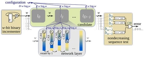
Sorting networks are of prime importance as circuits, with applications in sorting small data chunks, big data analytics, permuting packets, and system interconnects. Finding optimal sorting networks is a highly complex problem, and knowledge on optimal sorting networks is limited. When optimising the network depth or the number of comparators, one of the most expensive tasks is considered to be verification, that is, to verify that the candidate compare-and-swap network actually sorts the data. This grows exponentially with the size of the sorting network. However, FPGAs allow vast amounts of internal parallelism, and our presented work exploits this flexibility using dataflow techniques to achieve unparalleled amounts of speedup for sorting network verification. This work can be used in a modular way to accelerate the search for optimal sorting networks with a high number of inputs, as well for similar verification problems.

4 February 2026

Sorting network verification circuit processing a single input sequence per cycle.

A Review of Thermal Management Techniques Adopted for High-Power-Density GaN-Based Converters

  • Mohamed Belguith,
  • Sonia Eloued and
  • Mahmoud Hamouda
  • + 2 authors

Power converters based on gallium nitride (GaN) are progressing swiftly owing to their exceptional efficiency and tiny dimensions, boosted by high power density and fast switching capabilities. Nevertheless, these benefits are accompanied by considerable thermal management issues that impact reliability, performance, and operational lifespan. This review examines advanced thermal management approaches for high-power-density GaN power converters, including active and passive cooling technologies, sophisticated packaging designs, and the use of novel materials like graphene and diamond to improve heat dissipation. The impacts of thermal boundary resistance, self-heating phenomena, and substrate selection on thermal performance are thoroughly analyzed. Strategies for enhancing printed circuit board (PCB) layouts, thermal vias, and the use of thermal interface materials (TIMs) are also emphasized. The study highlights co-design approaches that optimize thermal resistance and layout efficiency, supporting GaN operation under high-frequency conditions. This thorough investigation offers insights into addressing the thermal challenges linked to GaN technology, promoting its adoption in forthcoming power devices.

22 January 2026

Overview of thermal management approaches in power electronics, including active and passive techniques.

Neuromorphic computing, an interdisciplinary field combining neuroscience and computer science, aims to create efficient, bio-inspired systems. Different from von Neumann architectures, neuromorphic systems integrate memory and processing units to enable parallel, event-driven computation. By simulating the behavior of biological neurons and networks, these systems excel in tasks like pattern recognition, perception, and decision-making. Neuromorphic computing chips, which operate similarly to the human brain, offer significant potential for enhancing the performance and energy efficiency of bio-inspired algorithms. This review introduces a novel five-dimensional comparative framework—process technology, scale, power consumption, neuronal models, and architectural features—that systematically categorizes and contrasts neuromorphic implementations beyond existing surveys. We analyze notable neuromorphic chips, such as BrainScaleS, SpiNNaker, TrueNorth, and Loihi, comparing their scale, power consumption, and computational models. The paper also explores the applications of neuromorphic computing chips in artificial intelligence (AI), robotics, neuroscience, and adaptive control systems, while facing challenges related to hardware limitations, algorithms, and system scalability and integration.

22 January 2026

(a) The first generation: perceptron. (b) The second generation: MLPs. (c) The third generation: SNNs.

A Procedure for Fast Circuit Cross Section Estimation

  • Clayton R. Farias,
  • Tiago R. Balen and
  • Paulo F. Butzen

Semiconductor technologies are susceptible to radiation effects. The particle incidence in susceptible areas of an integrated circuit (IC) can generate physical interactions capable of producing errors. This paper predicts the IC cross sections for Single Event Effects. The cross section is a metric that provides an IC’s susceptibility to radiation. It deals with particle source interaction and physical design volumes. This work evaluates the IC cross section, exploring the physical design characteristics of susceptible regions in logic gates. It explores particles with low LET, identifying the charge collection areas. Also, the heavy ions are used to evaluate the critical cross section range. Distinct benchmark circuits were simulated to characterize sensitivity trends. The influence of circuit input conditions along with cells’ susceptibility reveals significant findings. The results indicate a difference up to ten times between low- and high-energy particles. Consequently, predicting the IC cross section at an early stage of the design flow is essential, especially for electronics devices used in radiation environments.

13 January 2026

Layout of NAND2 in 45nm technology: the complete layout on the left and only visible layer 1 (active area), 9 (poly-silicon), 10 (contacts), and 11 (metal supply and ground connections) in the middle [33].

News & Conferences

Issues

Open for Submission

Editor's Choice

Get Alerted

Add your email address to receive forthcoming issues of this journal.

XFacebookLinkedIn
Chips - ISSN 2674-0729