1. Introduction
Technological innovation is an essential element in improving the quality of our daily lives. In particular, wearable electronic devices are becoming a reality on the technology market for a wide range of applications: physiological signal monitoring, environmental sensing, visual signaling, work safety, etc. [
1,
2,
3]. Wearable devices can be divided into three different categories: accessories (smart watches, smart glasses, etc.), e-textiles (sensors on textiles, fibertronics), and e-patches (sensor patches, e-tattoo, e-skin) [
4,
5]. Among these, textiles, due to their ubiquity in our daily life, represent an interesting platform for the integration of new functionalities. Thanks to the technological evolution, electronic devices are no longer rigid and bulky systems but can be extremely flexible, light, and low-cost, making them easy to integrate into our clothing. Various devices have already been integrated into fabrics: energy storage devices [
6], electrochemical transistors [
7], energy nanogenerators [
8], capacitive chemical sensors [
9], solar cells [
10], etc. In this context, light-emitting devices and integrated fabric displays represent an interesting application due to their capability to directly transmit visual information. All the possible device architectures and technological aspects related to the integration of light emission into textiles have been widely reported [
11]. Organic light-emitting diodes (OLEDs) are one of the most promising technologies for light-emitting textiles due to their nanometer thickness and the flexibility of organic materials. Encapsulated glass-based OLEDs and flexible OLEDs fabricated on top of high-barrier substrates have been integrated into textiles, but in such cases the level of integration is very low and the flexibility and/or conformability of the devices with the fabric are compromised [
12]. Another strategy is to fabricate fiber-based OLEDs, where each layer is deposited directly onto a single fiber using thermal evaporation [
13] or dip-coating methods [
12,
14,
15,
16]. Unfortunately, the latter approach is extremely expensive, as each fiber needs to be functionalized prior to textile fabrication. Furthermore, with the aim of integrating the electroluminescent fibers into a fabric, the fibers and the whole device should be robust enough to be processed like standard fibers (weaving, knitting, etc.), so it must meet some additional mechanical requirements. An alternative hybrid approach is to fabricate OLEDs directly on textile substrates. Due to the discontinuous surface and the high roughness of the fabric, a suitable modification of its surface is mandatory prior to OLED fabrication. This planarization phase is one of the most important processes that determines the performance of this type of fabric-based OLEDs. Fabric planarization provides a defect-free continuous surface that can compensate for the wavy morphology of the fabric while maintaining its flexibility and lightness. Several planarization processes have been reported in the literature, and the planarized substrates have been successfully tested for the fabrication of OLED devices [
11].
Both thermally deposited and solution-processed textile OLEDs have been reported by Prof. Choi’s group. They used a thin polymer film thermally laminated onto the fabric as a planarization layer [
17,
18]. An alternative planarization method has been demonstrated by the same group, which consists of laminating a polyurethane film at room temperature under low pressure. In particular, the planarizing film is composed of two different layers: the first one, in direct contact with the fabric, has a low viscosity and is used to remove the large-scale roughness; the second layer has a high viscosity and is employed to ensure a flat surface [
19,
20]. In 2016, an improvement on this planarization method was reported, consisting in the use of a guide substrate for the application of the high-viscosity PU layer [
21]. In the same year, Song et al. reported the fabrication of an AMOLED panel driven by OTFTs on a polyethylene textile substrate [
22]. In this study, the fabric was planarized by using a two-step process with two different materials: polyurethane (PU) and photo-acrylic (PA). A new technology based on a stress-reducing textile platform has recently been reported, using a thin SU8 layer and an elastomeric strain buffer layer to reduce mechanical stress [
23]. Another approach is to use UV-curable resins as planarization materials, and an efficient flexible top-emitting OLED has been fabricated on a silk fabric whose surface has been smoothed by spin-coating with a UV-curable resin [
24]. Recently, the latter approach has been used to develop an improved planarization method based on the template-stripping process [
25].
Table 1 summarizes all the mentioned planarization methods, together with the device architecture, deposition techniques, and performance. As can be seen from such a table, most of the planarization methods are not fully industrially scalable because they involve multi-step processes and/or laboratory scale deposition (e.g., spin coating).
Moreover, most textile-based OLEDs reported in the literature are top-emitting, using a bottom electrode based on a reflective metal and a semi-transparent top electrode. Two examples of bottom-emitting textile-based OLEDs were reported by Sohn et al. by using a sputtered ITO as the bottom electrode and a reflective top electrode [
26] and by Kim et al. with a PEDOT:PSS-based anode [
18]. Fully transparent devices have also been obtained by using very thin metal films [
27] and dielectric/metal/dielectric electrodes [
28].
In this context, we report the development of a simple and efficient planarization method, which exploits the blade coating deposition of a liquid resin and a silicon “guide substrate” to obtain a fabric with a very low surface roughness. In particular, UV-curing resins with different viscosities were employed to study the effect of viscosity on the morphological and mechanical properties of the planarized fabric, and the best substrates for the fabrication of transparent OLED devices were tested, achieving luminance values higher than 3000 cd/m2 and a current efficiency of 9.3 cd/A. The reliability and mechanical durability of the devices were tested by evaluating the electro-optical performance before and after bending cycles. Such planarization techniques can be easily industrially scalable for the possible implementation of this process with those typically used in the fabric industry. In fact, if the planarization method and the device fabrication process can be carried out using high throughput and easily scalable coating techniques, it is in principle possible to develop a pilot line for the entire fabrication process of fabric-based OLEDs.
In addition, the fabricated OLEDs are fully transparent, since they exploit a PEDOT:PSS anode and an Ag/WO3 semi-transparent bilayer as cathode. Fabricated OLEDs are fully transparent, since they exploit a PEDOT:PSS anode and an Ag/WO3 transparent bilayer as cathode. Fabric-based transparent devices can be particularly interesting from an aesthetic point of view, and in our case, we combined them with fluorescent fabrics to down-convert the colour emitted by the device. Such an approach could be very useful to achieve white emission from a very simple structure.
Therefore, considering all these features, the advantages/innovations of our fabric-based OLEDs are the following:
- -
industrial scalable planarization method based on blade-coating deposition;
- -
fully transparent OLEDs that exploit a polymeric anode
- -
down-converting approach to easily tune the colour emitted by the device.
2. Experimental Section
2.1. Materials
The UV-curable resins (NOA 61, NOA 65 and NOA 68) were supplied by Norland Products Inc (Jamesburg, NJ, USA), Vektron (100% Polyester, 105 g/m2) and Carnival (100% Polyester, 110 g/m2, with conductive fibers) fabrics were supplied by Klopman International S.R.L. (Frosinone, Italy), Clevios PH1000 (PEDOT:PSS ratio = 1:2.5) was purchased from Heraeus Clevios GmbH (Leverkusen, Germany) and was used as anode. Cesium was supplied by Saes Getters (Milano, Italy). All the other employed materials in the OLED device, N,N,N′,N′-Tetrakis (4-methoxyphenyl)benzidine (MeOTPD), 2,3,5,6-Tetrafluoro-7,7,8,8tetracyanoquinodimethane (F4TCNQ), 4,4′-Bis(N-carbazolyl)-1,1′-biphenyl (CBP), Tris [2-phenylpyridinato-C2,N]iridium(III)) (Ir(ppy)3), Batho-phenanthroline (BPhen), silver (Ag), and tungsten(VI) oxide (WO3) were purchased by Merck (Milano, Italy).
2.2. Planarization Method and OLED Fabrication
The planarization consists in a multi-step process. First, a known amount of resin (500 µL) is dropped on top of a flat rigid substrate (glass or silicon wafer); then a piece of fabric (3 × 3 cm2) is placed on top of the dropped resin to allow its impregnation. Finally, the resin is spread by blade coating at the interface between the rigid substrate and the fabric (also removing excess resin). The resin is cured by exposure to a UV lamp for 10 min. Finally, the fabric is peeled off from the rigid substrate and overturned, leaving a piece of fabric with a thin plastic layer on its surface. Pieces of planarized fabric (2.5 × 2.5 cm2) were cleaned with acetone and isopropyl alcohol, dried with nitrogen gas, and applied to a glass substrate. To further remove impurities from the flexible substrates and improve adhesion, a 2′ oxygen plasma treatment (50 W, 30 sscm) was performed on top of the substrates prior to OLED layer deposition. The OLED structure consists of the following components: PEDOT:PSS/MeOTPD p-doped (F4TCNQ)/MeOTPD/CBP:Ir(ppy)3 /BPhen/BPhen n-doped (Cs)/Ag/WO3. The anode layer consists in a thin film of PEDOT:PSS (100 nm) obtained by spin coating deposition (1000 rpm × 60″) of a commercial solution modified by the addition of 5% by volume of dimethylsulfoxide (DMSO) to improve the conductivity, followed by annealing at 120 °C for 1 h. Organic layers, Ag and WO3, were deposited by thermal evaporation in a Kurt J. Lesker multiple high vacuum chamber system.
2.3. Characterization
Morphological and cross-sectional images were obtained by scanning electron microscopy (Zeiss FE-SEM Merlin). Profilometer scans were performed using a surface profiler (Dektak) characterised by a mechanical stylus with a 12 μm tip diameter. The surface morphologies, including roughness parameters, were characterised using atomic force microscopy (no-contact mode, AFM PARK SYSTEMS XE-100).
The opto-electronic characteristics of the OLED devices were measured in a glove box by using an Optronics OL770 spectrometer coupled by an optical fiber to the OL610 telescope unit for the luminance measurements. The entire system was National Institute of Standards and Technology (NIST)-calibrated using a standard lamp and was connected to a Keithley 2420 current-voltage source meter via an RS232 cable. Bending tests were performed using a custom-made system to apply mechanical strain to the samples: After OLED fabrication, two opposite ends of a planarized fabric were constrained using two metal clamps, which were moved automatically so as to get closer to each other and induce bending of the device to a bending radius of 5 mm, at a bending frequency of 1 Hz.
3. Results and Discussion
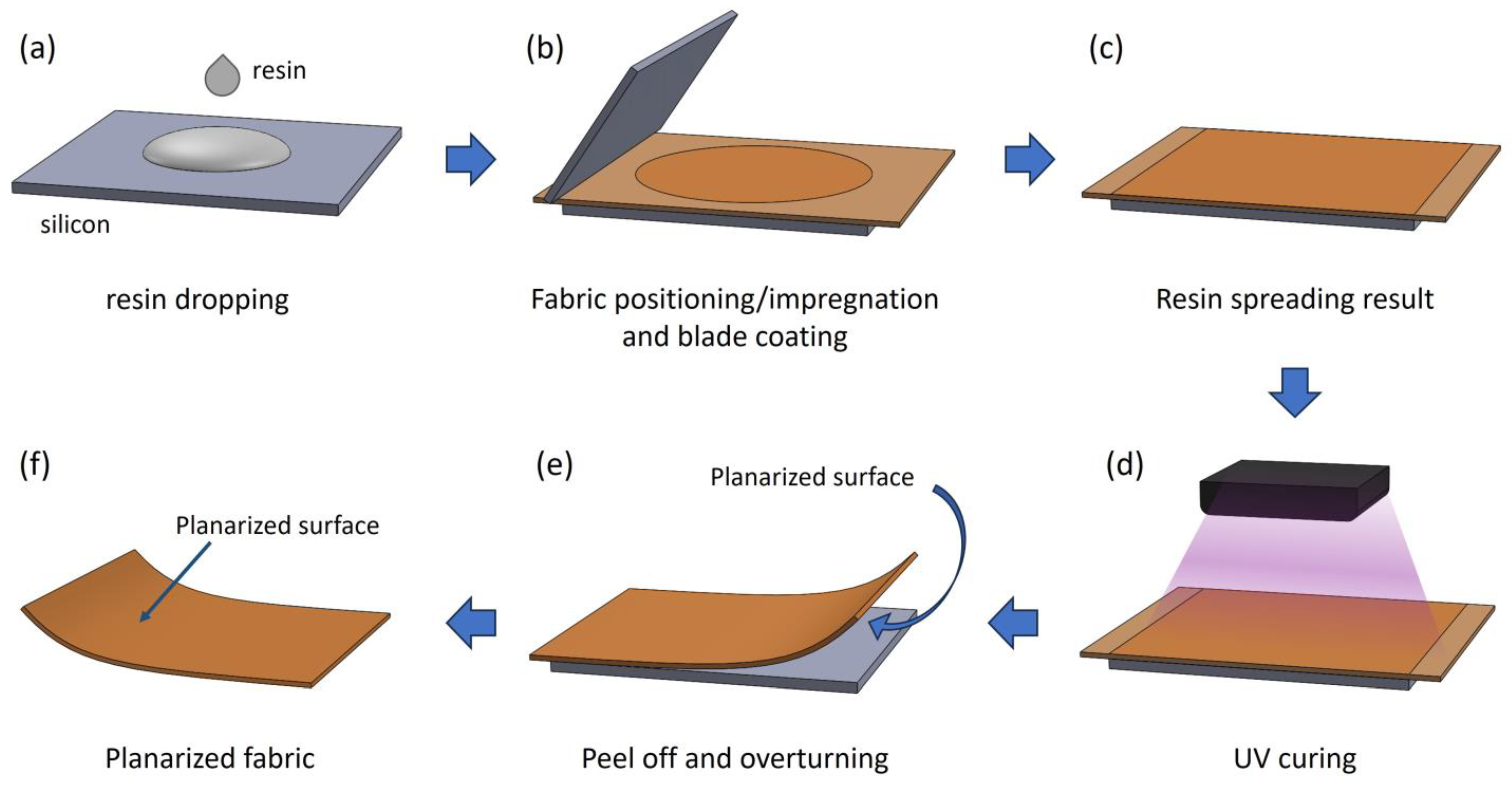
The planarization process is one of the most critical steps in the fabrication of fabric-based OLEDs and other types of wearable electronic devices. The main objective is to achieve a fabric surface that is as flat as possible, eliminating and compensating for the natural wavy structure of the fabric to make it suitable for the manufacture of OLED devices. In this context, a simple and fast planarization method has been developed. The method consists of a multi-step process and is shown schematically in
Figure 1.
First, a liquid resin is dropped onto a flat rigid “guide substrate” (silicon), with a very low surface roughness; then a fabric cutout is placed on top of the liquid resin in order to allow its impregnation; finally, the resin is spread at the interface between the rigid substrate and the fabric by blade coating. The resin is cross-linked by UV irradiation, and the fabric is then peeled off from the silicon substrate. This results in the transfer of surface morphological properties from the silicon to the planarizing resin, resulting in a perfectly flat and defect-free polymer layer that is intrinsically integrated with the fabric.
The process is compatible with any type of liquid resin, but it is obviously preferable to select materials with good mechanical, thermal, and chemical properties to suit the application. Either UV-curable or thermosetting resins can be used. For UV curing, if the fabric has thickness and mesh that allow UV radiation to pass through, silicon can be used as a ‘guide substrate,’ and the UV lamp is positioned on top of the fabric; conversely, a UV transparent substrate can be used as an alternative “guide substrate” (glass, quartz, etc.). In this study, three UV-curable commercial resins (NOA 61, NOA 65, and NOA 68) and two types of fabrics (Vektron and Carnival) were selected to validate the planarization method using silicon as the planarization substrate. The rheological and mechanical properties of the selected resins are reported in
Table 2.
All three materials selected have good flexibility and are suitable for the application. In particular, the three resins were chosen because they have very different viscosities in order to test the effect of such properties on the quality of the planarization layer. The thicknesses of the fabrics before and after the planarization with the different resins selected are given in
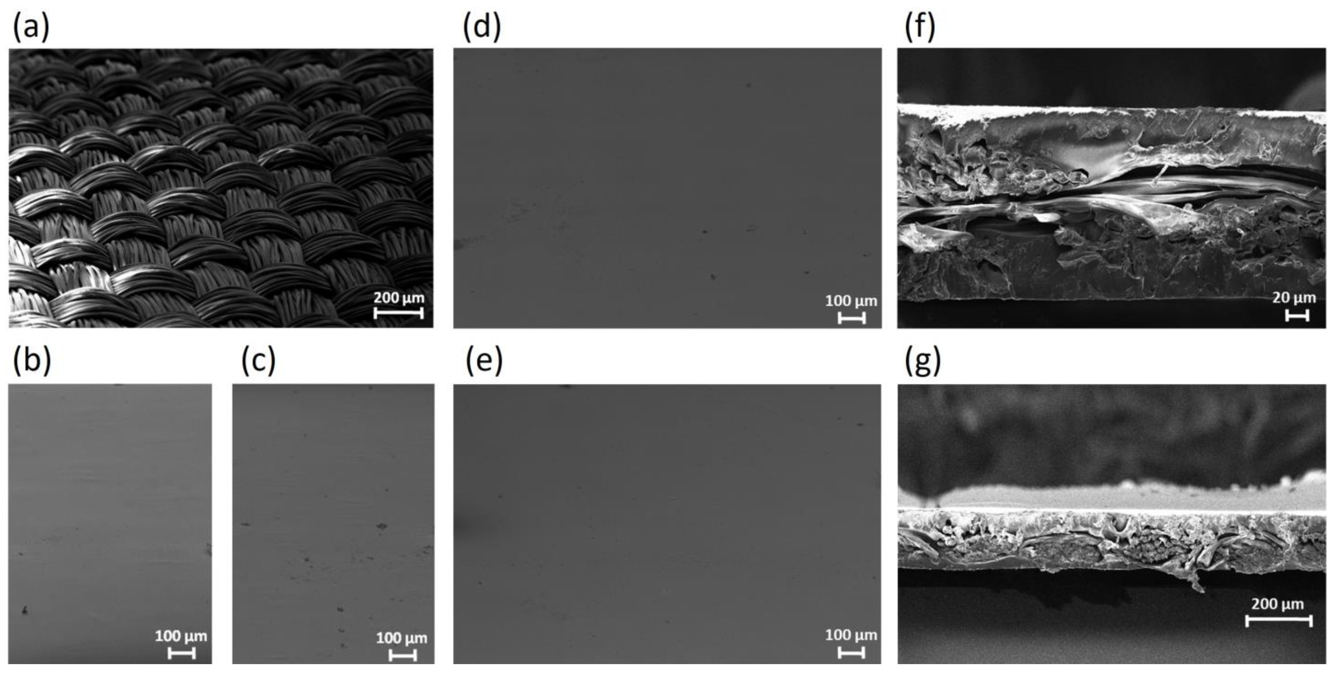
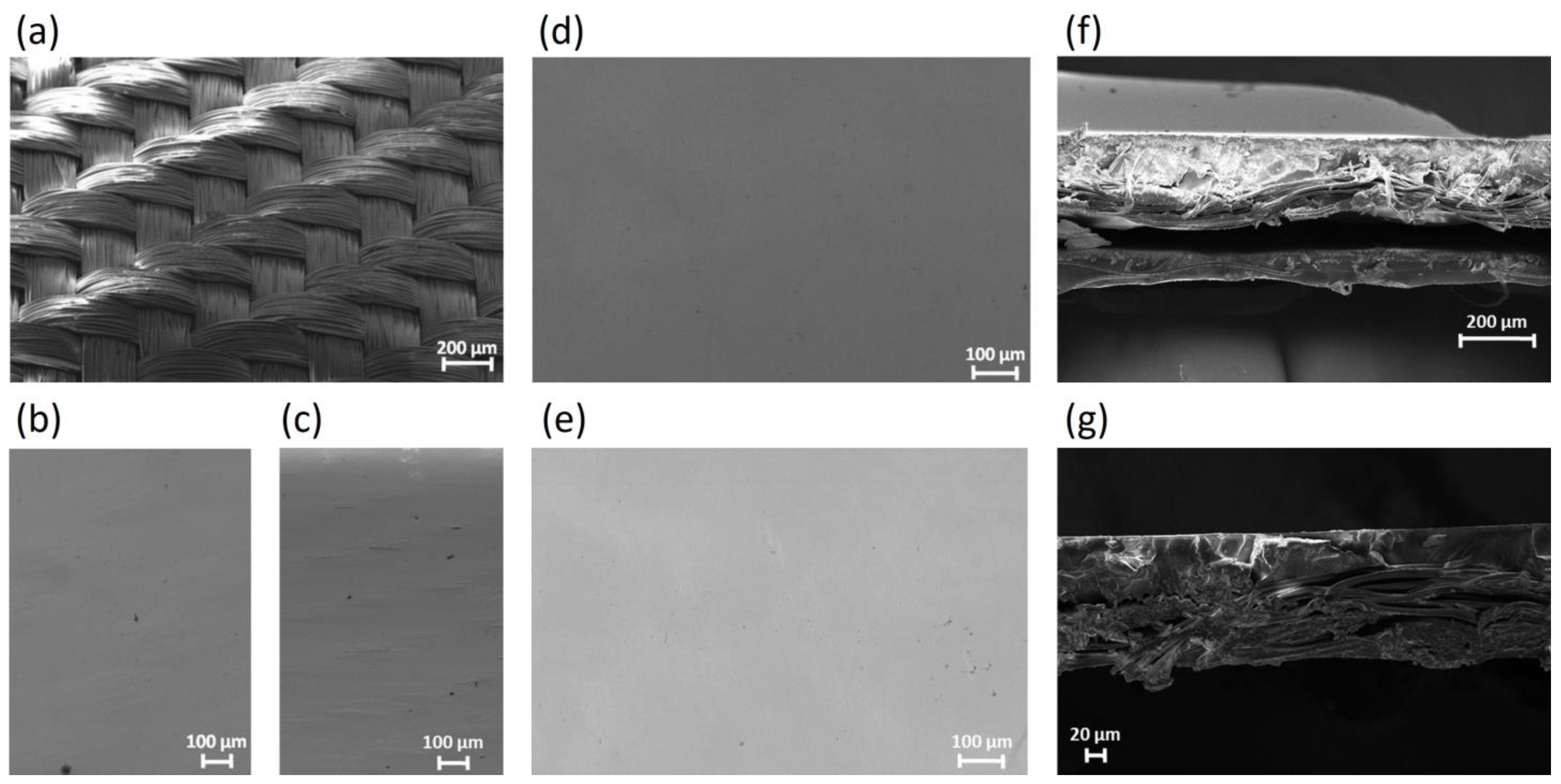
Table 3, while SEM images of the fabric surface before and after planarization are shown in
Figure 2 and
Figure 3. In order better to evaluate the three-dimensional characteristics of the fabric surfaces, the samples were tilted during the SEM measurements.
The classic weft-warp interlaced structure is visible for both types of fabric (
Figure 2a and
Figure 3a), which is also confirmed by the profilometer scans reported in
Figure S1a,c. Instead, a completely different morphology appears after the planarization, as shown in
Figure 2 and
Figure 3. In particular, the surface of the fabrics planarized with NOA 61 still shows the underlying fibers. This effect is minimized by using NOA 65 resin, until it disappears completely with NOA 68. The fabric planarized with NOA 68 shows a very smooth surface, which is ideal as a substrate for OLED fabrication. We attribute this behavior to the variation in resin viscosity: low-viscosity resins tend to be absorbed more easily by the fabric, and the thickness of the outer layer of the resin after the blade coating is not sufficient to ensure a good surface uniformity, leaving some fibers exposed. As the viscosity increases, the resin encounters greater resistance to penetrate into the fibers, and the amount of resin that does not penetrate into the fabric ensures the formation of a homogeneous layer, thick enough to cover the sample surface uniformly, resulting in effective planarization.
This hypothesis is also confirmed by the different thicknesses of the planarized fabrics (
Table 3); although the same quantity of resin is being used for the different samples and the deposition is carried out with the same parameters, the greater thickness is obtained with NOA 68 because less resin penetrates into the fabric.
With the aim of reducing the thickness and improving the flexibility of the planarization layer while maintaining a smooth and uniform surface, a bilayer approach was also tested. A bilayer consisting of a lower layer of NOA 65 and an upper layer of NOA 61 has a thickness of approximately 160–170 µm and the same morphology as observed for NOA 68 (
Figure 2e and
Figure 3e).
The profilometer scans of the planarized fabrics (
Figure S1b,d) confirm what was deduced from the SEM images. Indeed, all resins are able to strongly reduce the valleys– peaks height typical of the fabrics in the range of hundreds/thousands of nm. In particular, fabrics planarized with NOA 61 and NOA 65 show a significant wavy structure and defects due to fibres not being completely covered by the resin. Fabrics planarized with NOA 68 and NOA 65/NOA 61 are almost comparable, with a smooth wavy structure and absence of defects, and such characterisation confirms the suitability of such planarized fabrics for the fabrication of OLED devices. The AFM pictures and associated roughness values shown in
Figure S2 further confirm the possibility of fabricating OLED devices on such planarized fabrics.
The cross-sectional SEM images of the best sample are also shown (
Figure 2f,g and
Figure 3f,g). The fibers and the structure of the fabric are clearly visible together with a smooth and compact upper planarizing layer. The overall thicknesses of the fabric samples planarized with NOA 68 are significantly greater than those with NOA 65 + NOA 61. In addition, it appears that the resin NOA65 + NOA61 is better impregnated and adheres better to the fabric than NOA 68, which could be an advantage in terms of durability and flexibility.
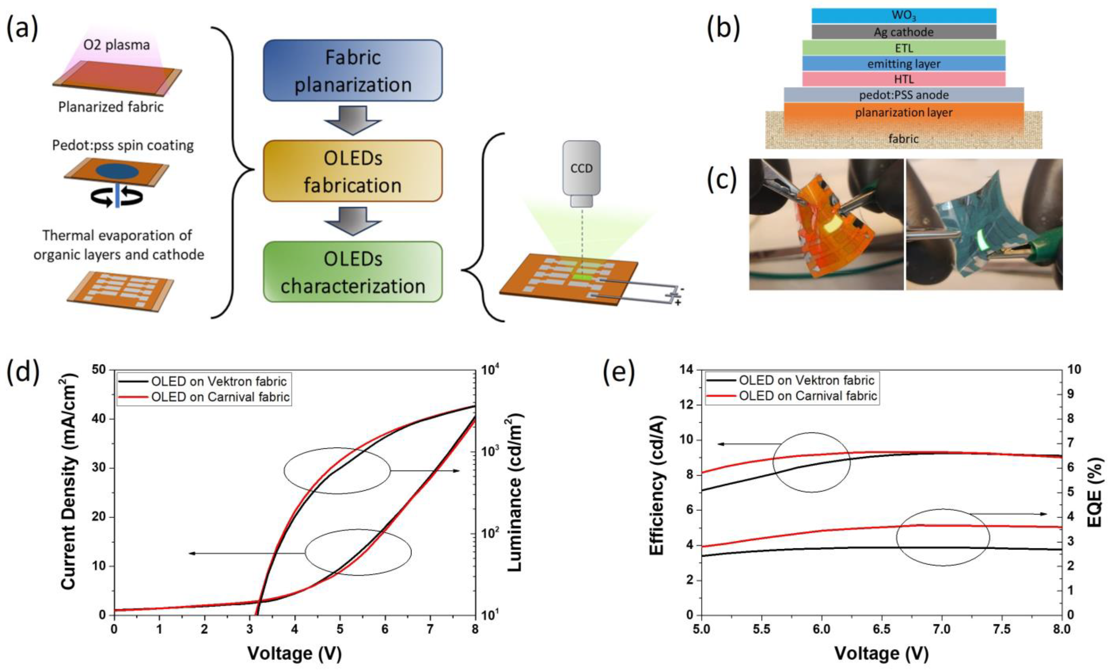
The planarized fabric based on NOA 68 and the bilayer NOA65/NOA61 were tested as flexible substrates for the fabrication of OLED devices. The structure of the devices is as follows: highly conductive (HC) PEDOT:PSS/Hole transport layer (HTL)/Emitting layer (EML)/Electron transport layer (ETL)/Ag/WO
3. Due to the limited visible transmittance of typical fabrics, a transparent top electrode is mandatory. In our case, a transparent cathode based on an Ag/WO
3 bilayer was employed [
29], and a polymeric electrode based on HC PEDOT:PSS was used as the bottom electrode, in order to improve the stability of the device [
30]. Both electrodes show high transmittance in the visible range, and therefore our devices can be considered fully transparent.
The HTL consists of N,N,N′,N′-Tetrakis(4-methoxyphenyl)benzidine (MeoTPD) p-doped with 2,3,5,6-Tetrafluoro-7,7,8,8-tetracyanoquinodimethane (F4TCNQ), the ETL of Bathophenanthroline (Bphen) n-doped with cesium (Cs). The EML is based on a host–guest system using CBP as the matrix and Ir(ppy)
3 (tris(2-phenylpyridine)iridium(III)) as the green emitting dopant. The electro-optical performance of all the prepared devices is reported in
Table 4, and the data for the best devices on top of the two different fabrics are shown in
Figure 4.
There are no significant differences between the two different planarization methods; the best device has a luminance of more than 3000 cd/m2 and a maximum current efficiency of 9.3 cd/A Since the PEDOT:PSS bottom electrode is transparent, the light emitted by the device is partially absorbed by the fabric, reducing the luminance, and therefore the efficiency of the device, compared to an analogue device with a reflective bottom electrode.
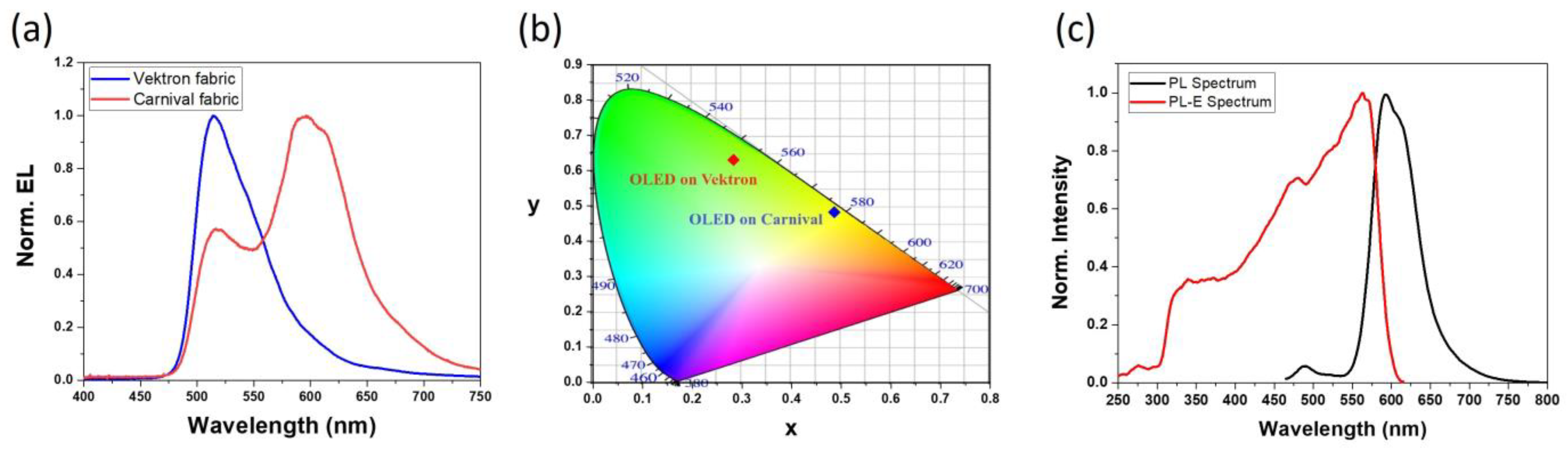
The electroluminescence spectra and the CIE coordinates of the two different types of device are shown in
Figure 5. As can be seen, the device fabricated on the Vektron fabric emits green light, whereas it emits orange light when fabricated on the Carnival fabric. This effect of color variation is due to a re-emission phenomenon on the part of the Carnival fabric. As both electrodes are transparent, light is emitted in all directions and partially absorbed by the fabric. In the case of Carnival, which is made of fluorescent material, the light emitted by the device is able to excite the fluorescent fabric and is re-emitted at a different wavelength, which is characteristic of the “fluorescent fabric”. The color emitted by the device on the “fluorescent fabric” is the result of the primary emission from the device and the re-emission phenomenon from the fabric. The excitation and emission spectra of the Carnival fabric are shown in
Figure 5c and confirm this theory. As a result, it is possible easily to tune the emitted color and even obtain white emission from a monochromatic blue device by using a fluorescent fabric and a transparent bottom electrode. In addition, the use of the “fluorescent fabric” makes it possible to improve the efficiency of the device by improving the quantity of photons emitted by the device. Indeed, whereas with the Vektron fabric the light emitted from the bottom of the device is simply absorbed by the substrate itself (and lost), with the Carnival fabric the light is partially absorbed and re-emitted in all directions, thus improving the total number of emitted photons. In support of this hypothesis, the EQE of devices fabricated on Carnival is higher than that of those fabricated on Vektron (see
Table 4). However, the effect of the efficiency improvement is not so evident from the current efficiency values, as luminance (cd/m
2) measures the luminous flux normalized to the sensitivity of the human eye, and therefore takes into account the emission wavelength (and the color). Moreover, the Vektron and Carnival fabrics could have small differences in terms of reflection, which slightly influences the emission spectrum. As a result, the “green” device has similar luminance values to the “orange” one, although the total number of photons reaching the detector is lower.
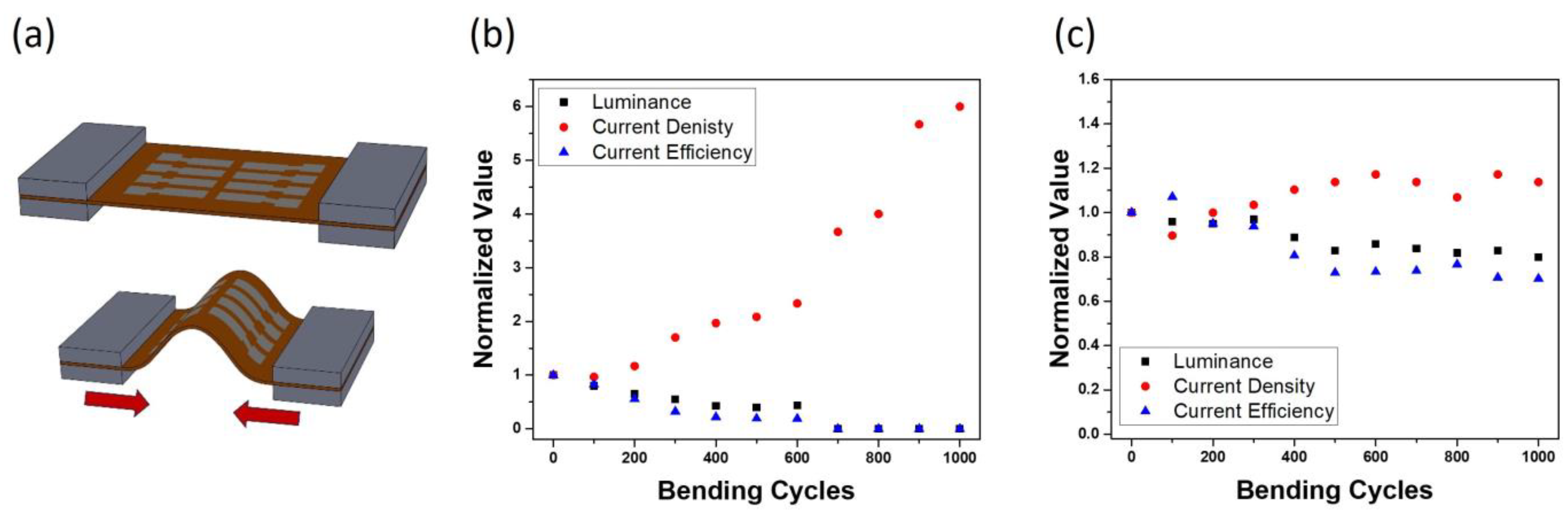
In terms of flexibility, the devices were tested under bending conditions. The variations in luminance, current density, and current efficiency versus bending cycles are reported in
Figure 6. The device manufactured on the NOA 68 planarized fabric degrades rapidly with the number of bending cycles, and there is a total failure of the device after about 600 cycles. Contrarily, the device on NOA 65 + NOA 61/fabric is much more stable and retains almost 80% of the luminance and 70% of the current efficiency of the pristine device after 1000 bending cycles at a bend radius of 5 mm.
Although the tested planarized fabrics have an equally smooth and defect-free surface, there is a significant difference in flexibility. This difference in behavior can be attributed to the thickness of the planarization layer; in fact, a greater thickness corresponds to improved stiffness and greater stress on the film and the entire device. The viscosity of the NOA 65 resin is such that it imparts good surface properties to the fabric, without excessively exceeding the thickness. A thin layer of NOA 61 on the surface of the NOA 65 can further improve the surface quality. The total thickness of the bilayer NOA 65 + NOA 61 is much lower than the planarization layer obtained with NOA 68, and this ensures good flexibility of the planarized fabric. The planarization based on NOA 68 gives a fabric with a high surface morphological quality, but the high thickness confers an excessive stiffness that reduces the fabric flexibility and the durability of the device. Considering the reported results, the planarization method based on the double layer deposition of NOA 65 and NOA 61 is the best solution for the fabrication of fabric-based OLEDs.
4. Conclusions
In this study, an innovative planarization process for textile-based electronic devices has been developed. The planarization is based on the deposition of a liquid resin at the interface between the textile and a “guide substrate” using a blade coating and subsequent cross-linking by UV radiation to obtain a solid polymeric layer on the surface of the fabric. The fabric is then peeled off the substrate together with the planarizing polymer layer. As a result, the smooth and uniform surface of the “guide substrate” is exactly replicated on the surface of the planarizing layer. The planarization process has been validated by using UV curable resins of different viscosities, and it has been observed that a higher viscosity (NOA 68 = 5000 CPS) is essential to ensure a good planarization layer. At the same time, a high viscosity corresponds to a high thickness of the planarization layer and excessive stiffness of the fabric. An alternative planarization method was tested by applying a double layer consisting of NOA 65 (1000 CPS) as the bottom layer and NOA 61 (300 CPS) as the top layer. These planarized fabrics were tested as substrates for the fabrication of textile-based OLED devices. The devices fabricated on top of the planarized fabrics show luminance values higher than 3000 cd/m2 and current efficiencies higher than 9 cd/A. It has also been shown that by using a “fluorescent fabric” and a transparent bottom electrode, it is possible to tune the color emission without changing the device architecture. This aspect may be interesting to obtain different colors and even white emission by using simple monochromatic emitting materials. In addition, such an approach can be used to improve the efficiency of the devices by increasing the number of photons emitted. The devices have been tested under bending conditions, and it has been observed that the device fabricated on the NOA 65 + NOA 61 bilayer retains almost 80% of its luminance and 70% of its current efficiency after 1000 bending cycles.
The reported results can be exploited for the development of wearable electronic devices by using high-throughput, simple, and low-cost deposition techniques. On the other hand, the proposed planarization method, although capable of transferring a good surface morphology to the planarization film, presents a limiting issue related to the generalization of the technique on any type of fabric. In fact, if the weft and warp of the fabric are too dense (reduced presence of voids), during the curing phase a large part of the UV radiation would be absorbed by the fabric itself and the polymerization of the resin might not take place completely. To overcome this issue, a transparent substrate (i.e., glass) could be used as a guide substrate instead of silicon, although a solution would have to be found to minimize the surface roughness of glass, which is known to be higher than that of silicon wafers. The improvement and generalization of the planarization technique proposed here will be investigated in future studies, with the aim of developing a process that is not limited by the type of woven fabric used.

 ,
, 


