
Residue Number System (RNS) and Power Distribution Network Topology-Based Mitigation of Power Side-Channel Attacks


Department of Electrical and Computer Engineering, Iowa State University, Ames, IA 50010, USA
*
Author to whom correspondence should be addressed.
Cryptography 2024, 8(1), 1; https://doi.org/10.3390/cryptography8010001 (registering DOI)
Submission received: 24 October 2023
/
Revised: 8 December 2023
/
Accepted: 19 December 2023
/
Published: 21 December 2023
(This article belongs to the Special Issue Feature Papers in Hardware Security II)
Abstract
:Over the past decade, significant research has been performed on power side-channel mitigation techniques. Logic families based on secret sharing schemes, such as t-private logic, that serve to secure cryptographic implementations against power side-channel attacks represent one such countermeasure. These mitigation techniques are applicable at various design abstraction levels—algorithm, architecture, logic, physical, and gate levels. One research question is when can the two mitigation techniques from different design abstraction levels be employed together gainfully? We explore this notion of the orthogonality of two mitigation techniques with respect to the RNS secure logic, a logic level power side-channel mitigation technique, and power distribution network (PDN), with the decoupling capacitance, a mitigation technique at physical level. Machine learning (ML) algorithms are employed to measure the effectiveness of power side-channel attacks in terms of the success rate of the adversary. The RNS protected LED block cipher round function is implemented as the test circuit in both tree-style and grid-style PDN using the FreePDK 45 nm technology library. The results show that the success rate of an unsecured base design 68.96% for naive Bayes, 67.44% with linear discriminant analysis, 67.51% for quadratic discriminant analysis, and 66.58% for support vector machine. It is reduced to a success rate of 19.68% for naive Bayes, 19.62% with linear discriminant analysis, 19.10% for quadratic discriminant analysis, and 10.54% in support vector machine. Grid-type PDN shows a slightly better reduction in success rate compared to the tree-style PDN.
1. Introduction
Hardware cryptanalysis techniques deployed in side-channel attacks (SCAs) exploit an asymmetry in some physical resource usage in an implementation to reveal a hidden or secret data value. The resources needed for an adversary to mount such a side-channel attack are relatively small. These side-channel attacks bypass the computational security of cryptographic algorithms to access confidential data. If two different key or subkey values exhibit the asymmetric or different measurements of a physical property, such as power [1], timing [2], electromagnetic radiation [3], or sound [4], the adversary is able to infer a partial value of the key or subkey. Power analysis has been shown to be an effective side-channel attack in integrated circuits [5]. This involves tapping the power pins / with low-impedance probes to detect data-dependent leakage. The adversary develops a power model of the secret data based on the correlations between the asymmetric power measurements and the values of a sub-word of secret data. A typical mitigation technique strives to remove this asymmetry—novel devices that consume data-independent energy interconnect to consume data-independent energy, or logic design styles whose energy is data-independent. Since the physics of the nature is not perfectly symmetric, the goal of these mitigation techniques is to remove data-dependent asymmetry to the extent that asymmetry measurements are prohibitively expensive for the adversary or are not feasible with the current measurement technology.
The first successful power side-channel attack tamper-resistant devices [1] were reported by Kocher et al. in 1999. Since then, many researchers have demonstrated several techniques such as template attack [6], correlation-enhanced power analysis collision attack [7], and many others that all exploit the data-dependent switching activity power measurements at the power pin. These data-dependent power models’ effectiveness can be reduced by making the power consumption profile independent of any data values. Cryptographic encryption algorithms make the relationship between plaintext and ciphertext close to random, seemingly eliminating the dependence between the known plaintext values and the switching activity induced by the ciphertext [8,9]. It may seem to reduce the effectiveness of power side-channel attacks, but it does not eliminate the statistical correlation between the observed power due to computational activity of the ciphertext and plaintext data.
The applicability of the power side-channel attacks is on the rise, even within the emerging computational infrastructure [10]. Internet of Things (IoT) devices are naturally susceptible to side-channel attacks since an adversary may have physical access to these devices on the edge. The cloud computing infrastructure seemed to be beyond the reach of power side-channel attacks due to the inability of an adversary to attach digital sampling probes to the power pins of a cloud rack. Zhao and Suh [11], however, devised a remote power side-channel attack on a cloud rack. With the wide adoption of SoC chips containing both hard-wired processing cores and reconfigurable fabric in the cloud, co-resident cloud threads hosted by either a processor core or reconfigurable logic may share a power domain. When the victim process performs significant computation, leading up to high level of switching activity, the corresponding power domain experiences a larger drop from the pin to the actual drains. The logic gates in this power domain will experience higher delay due to this drop. In the shared power domain reconfigurable logic, a time-to-digital converter (TDC) can be built to sample this delay as a proxy remote power measurement device. Such TDCs have been able to leak the secret key of AES encryption algorithm.
These attacks can be ameliorated if the intermediate values are randomized or obscured to reduce the correlation between the data and the power consumption of the device. The side-channel countermeasure techniques usually utilize an input encoding function to accomplish this purpose. The input encoding process converts the data into encrypted shares, providing both cryptographic and side-channel privacy. This ensures that the data do not leak through side channels. Cryptographic privacy is the difficulty of deciphering encrypted data using traditional cryptanalysis methods. In addition, the output of the encoding function has another interesting feature called the privacy against the side-channel. This is the difference in the data leakage through the power-channel side channel when the secret data are replaced from “0” to “1”. This is the traditional differential entropy used in defining differential privacy [12]. The encoding of input data is meant to obscure power consumption so that the power side-channel observations of the computations based on input values “0” and “1” cannot be distinguished.
Over the last two decades, several countermeasure techniques have been developed, broadly classified into two categories: masking and hiding. The masking countermeasure techniques randomize the intermediate values. This introduces shared or per-intermediate-value random variables during the design. It tends to reduce the correlation in the switching activity of the randomized intermediate variable, computationally derived from the secret value, and the secret value. The secret-sharing scheme [13] is a widely used masking countermeasure based on cryptography for multiparty computation and secret sharing. Ishai et al. [14] developed a bit-level secret sharing technique by splitting each input bit into shares. Each input bit x is encoded into shares. The first t shares are t random values , , , …, . The st share is computed as ⊕⊕⊕⊕ … ⊕. All the shares are needed to reconstruct x. Moreover, these shares are statistically not correlated. An adversary capable of probing up to t circuit nodes in each clock cycle is not able to learn the bit x. In one sense, the t-private circuits can thwart a more powerful adversary, one who can probe up to t internal circuit nodes each clock cycle, than the power side-channel adversary. Hence, it is cryptographically private against up to t probes. However, the computations of all the shares aggregated together still contain the switching activity of the original bit x leading a or higher-order power side-channel to capture some correlation between the secret bit x and the power signatures. Hence, the t-private schema may not be side-channel private.
Countermeasure techniques to obscure the power attempt to maintain the power level constant across different intermediate values during the computation. They do not need additional random values for input or intermediate value encoding as in masking. Different logic design styles to support constant power consumption for the intermediate values with dual-rail logic include sense amplifier-based logic (SABL) [15,16] and wave dynamic differential logic (WDDL) [17]. Dual-rail logic encodes each input as a pair of wires, one with the original signal and the other with its inverse. There are two stages of operation: the pre-charge phase and the evaluation phase. During the pre-charge phase, the voltage or value on the complementary wires are set to the pre-charge voltage. In the evaluation stage, the voltage or value of the complementary wire is determined by logical operations. After the evaluation stage, the value of the complementary wire is set to either (0, 1) or (1, 0) based on the input data, leading to exactly one of the dual rail outputs to switch regardless of the inputs. This leads to consistent data-independent gate level power consumption for the computation of any intermediate values.
Many other devices such as all-spin logic (ASL), memristor technology, and silicon nanowire FETs (SiNWFETs) exhibit more uniform power consumption over all possible switching states, and are hence better-suited for power side-channel attack mitigation. Cryptographic implementations with these device technologies are likely to achieve better security against power side-channel attacks. In [18], Alasad et al. demonstrated the potential of ASL in creating AES circuits resilient to power side-channel attacks. ASL’s distinctive feature of uniform power consumption, regardless of input or output, poses a challenge for PSC attack strategies. Similarly, Khedkar et al. [19] suggested a method that involves using a combination of complementary memristor-based resistive random access memory (RRAM) modules to ensure power traces in AES are balanced, thus making it difficult for DPA attacks to succeed. This approach involves incorporating a dual-state RRAM alongside the main memory, which helps in evenly distributing the power consumption and prevents unauthorized access to information through power profiles. In [20], Giacomin et al. proposed the use of compact silicon nanowire FETs with three independent gates to implement complementary logic in a way that minimizes power variations in input signals, thereby enhancing security against side-channel attacks. This technology, known as SiNWFETs, allows designers to include extra complementary logic, balancing power traces and maintaining a consistent power profile.
1.1. Motivation
t-private circuits offer cryptographic privacy, but very limited side-channel privacy. The side-channel privacy holds only for an adversary limited to up to tth order power side-channel attacks. Dual rail logic provides strong side-channel privacy, but no cryptographic privacy. The RNS logic [21,22] combines both side-channel privacy and cryptographic privacy. There is an average reduction of 25% in the adversary’s machine learning success rate in leaking a block encryption secret with the RNS logic.
Note that the asymmetries in switching or switched capacitance are introduced at many abstraction levels—algorithm, architecture, logic, physical placement, layout, and devices. All these design flow layers have to strive to provide data-independent power or other physical side-channel behavior. Towards that end, we introduced the addition of decoupling capacitances to the power distribution network as a power side-channel mitigation technique at physical placement and the layout level [23]. We show that there is a significant reduction in the adversary power side-channel success rate with such a decoupling capacitance in a power tree. Specifically, the power side-channel success rate goes down from approximately 88% with no decoupling capacitance to 15% with 12 pf decoupling capacitance.
Both of these techniques work at different abstraction levels—RNS logic at the logic level and the decoupling capacitance at physical design level. An interesting research question that arises in such situations is: are these techniques orthogonal or are they correlated? If they were to be orthogonal, significant additive gains in side-channel resistance can be realized by adding a second technique to a design that has already integrated a first mitigation technique. If they were correlated, no such significant advantages may accrue. We raised this question with respect to RNS logic and the decoupling capacitance power distribution network as a preliminary answer to a more general question for a collection of multiple abstraction level mitigation techniques.
A second research question addressed in this paper pertains to power distribution networks. Our original paper [23] illustrates the effectiveness of decoupling capacitances in a tree power distribution network. Tree power distribution networks were popular in the 1980s and 1990s. A grid style power distribution network is a more common choice in recent designs. An interesting question is that of whether the decoupling capacitance as a power side-channel mitigation technique is specific to the topology of the power distribution network? Is it more effective in one topology than the others? We had performed a preliminary assessment of power side-channel mitigation through decoupling capacitance in a grid PDN in [23]. We answer this question more completely in this paper to show that the effectiveness of the decoupling capacitance is dependent on the power distribution network topology. Specifically, a grid power distribution network is more effective at mitigating power side-channels than tree power distributions networks.
This leads to yet another research question: is the only way to compare the two power distribution network topologies to perform detailed SPICE-level simulations of power side-channel leakage? We develop an analytical technique for a first order comparison of two power distribution network topologies, back of the envelope calculation, in Section 4.
1.2. Contributions
In this paper, the orthogonality of two power side-channel mitigation techniques, one at the logic level, RNS logic [21], and the other at the physical design level, decoupling capacitance in the power distribution network, is explored. The RNS logic is a logic style based on a secret-sharing scheme derived from residues, which also offers homomorphic encryption. Security-aware PDN is a side-channel attack (SCA) countermeasure technique employed during the physical design phase that places a decoupling capacitance along the power path to reduce data-dependent leakage reaching external . The power signature of the circuit switching activity is abstracted as a characteristic vector originating at a logic block node. This characteristic vector propagates through the PDN to the power pins. The characteristic vector visible at the power pins is used by a power side-channel adversary to infer the secret data. We need heuristics for propagating features from logic blocks to power pins through the PDN with the decoupling capacitance. The RNS protecting the LED block cipher round function is implemented as the test circuit in both tree-style and grid-style PDN using the North Carolina State University (NCSU) FreePDK 45 nm technology library. The side-channel resistance is evaluated by the success rates of machine learning classifiers such as naive Bayes (NB), linear discriminant analysis (LDA), quadratic discriminant analysis (QDA), and support vector machine (SVM) trained with the feature vectors. We also evaluate the area and security trade-offs of power distribution networks with decoupling capacitance. In summary, the key contributions are:
- 1.
- An analytical feature vector propagation-based model for a quick and dirty power distribution network power side-channel vulnerability evaluation.
- 2.
- A KCL-based algebraic model of a power distribution network whose algebraic power/degree is an indicator of the ease of learning of this model, particularly the machine learning’s accuracy in determining the secret from power feature vector samples. This allows a designer to assess and compare two alternative PDN topologies for power side-channel vulnerabilities without undertaking extensive SPICE level simulations. This again provides a quick discriminant for power distribution network evaluation.
- 3.
- Established through analytical modeling as well as empirical ML evaluation the superiority of grid PDN over tree PDN in suppressing power feature vectors.
- 4.
- Demonstrating that the RNS logic style and PDN integrating decoupling capacitance are two orthogonal techniques with respect to the power side-channel feature vector suppression. This means that the benefits of deploying the two techniques are mostly additive. The broader message from this observation is that several power side-channel mitigation techniques from various design abstraction levels—architecture, logic, physical, device—could be used together to provide additive benefits.
1.3. Paper Organization
This paper is organized as follows. In Section 2, a summary of the power distribution networks and related research is provided. Additionally, a brief overview of relevant background information is included. In Section 3, the basic principles of an RNS secure logic are described. The propagation of the data leakage feature vector in a power distribution network is discussed in Section 4. Section 5 presents a practical implementation of the RNS protected algorithm in different PDN topologies and the corresponding results with respect to the machine learning success rate. Finally, Section 6 summarizes and concludes the paper.
2. Background and Related Works
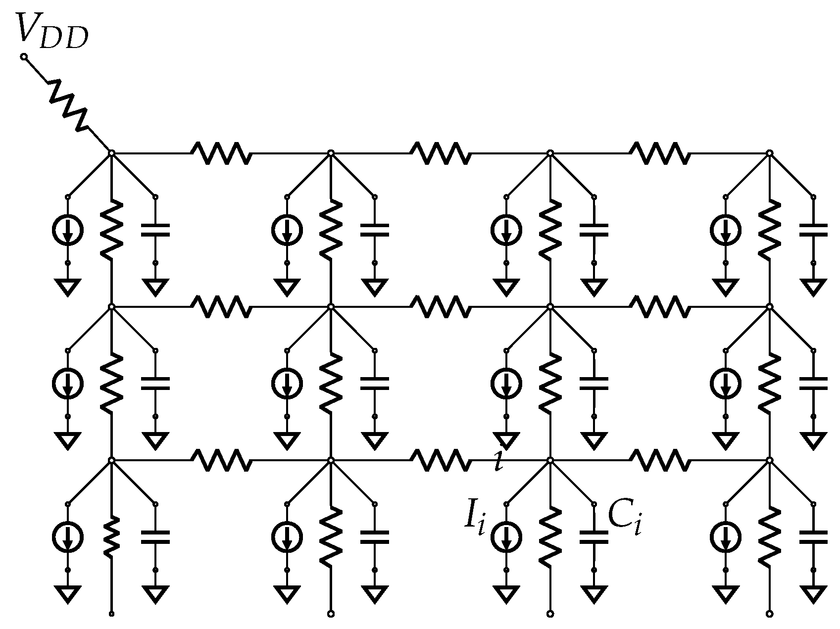
As the number of nets and gates continues to increase, it is becoming more difficult to provide all the transistor source and drain terminals with consistent and satisfactory and with a reasonable voltage drop. An excessive drop can reduce the swing voltage across a CMOS gate resulting in increased delay, increased short circuit current, the introduction of race conditions, and other undesirable characteristics. A power distribution network is responsible for maintaining acceptable drops and hence is a critical component in today’s integrated circuits. It is responsible for connecting logic cells to the / pin. The electrical power and ground buses on the chip are routed in Metal-1 or Metal-2 layers. A basic circuit is used to model the metal interconnections, as demonstrated in Figure 1. The current symbol at each node represents the current demands of the corresponding logic block. The main goals of the power distribution network are to ensure that a steady voltage is supplied to all logic cells, with low noise levels to meet their peak and average current draw requirements. The PDN is designed with low resistance in the metal layer to minimize losses.
Let node i experience a signal transition resulting in the current drawn from the power source, denoted in Figure 1. The external pin is connected to all the internal nodes with minimal voltage drop. Even though the external power pins are kept at voltage , the internal node voltage changes in response to the switching activity of the logic node. A high level of switching activity results in a higher current draw, which causes the voltage in the logic block to be . The external power pin’s current draw is a time-dependent variable varying in response to the logic block’s activity, which is transmitted through the power distribution network. The connection between the internal logic node i and the external pin also sources the current for other logic nodes at various junction points along the path. More common power path topologies between external pin and logic nodes i are in a tree or a grid style. The structure of the on-chip PDN design plays an important role in satisfying the design’s electrical characteristics requirements. In tree-style PDNs, each logic node has exactly one dedicated power path to . The tree-style PDN design supports limited interconnection resource requirements for low-cost ICs. On the other hand, a grid-style PDN connects logic nodes and with multiple paths. This provides a robust and high-performance current distribution network for high-speed integrated circuits, although at a higher interconnect cost than a tree-style PDN.
Most of the research efforts in PDN design focus on modeling IR drop [24,25,26] and power switching noise [27,28]. These models are used to iteratively refine the PDN design for low voltage drop and noise. In 2014, Mayhew and Muresan proposed a countermeasure technique by placing an nMOS gate capacitance near the logic block [29,30]. The nMOS capacitance temporarily supplies the current as needed and separates the logic block from the power distribution network. Dofe and Yu conducted a correlation power analysis attack and presented a success value indicator to assess the effectiveness of the countermeasure. In 2018, they proposed a correlation power analysis attack in 3D ICs that exploit power distribution noise [31]. The following year, Kenarangi et al. presented an on-chip sensor to detect power analysis attacks in real-time by monitoring the voltage variation on the power distribution network [32]. Additionally, Muresan et al. proposed a CMOS-based self-decoupling battery cell system to power security-sensitive modules when the voltage drops to a minimum threshold [33]. This research examines the impact of various power distribution networks and distributed decoupling capacitance on power side-channel attacks. Additionally, it looks at the random scheduling of the decoupling capacitance and the sampling requirements for the adversary to construct machine learning models. It is distinct from other studies in that it goes beyond the runtime detection of power analysis attacks.
Higher-Order Attacks
Higher-order side-channel analysis (HO-SCA) is a form of physical cryptanalysis that takes advantage of the combined leakage of multiple individual shares through power consumption. It is mainly used to thwart a system that is protected against first-order power analysis attacks [34]. Messerges et al. demonstrated the first higher-order SCA in the software implementation of the crypto-algorithms and on the ST16 smartcard. This study employs higher-order statistical moments to uncover the secret value of a cryptographic algorithm. Later in 2005, Mangard et al. stated that glitches contributed to significant power consumption and showed a theoretical analysis of DPA resistance in masked gates [35]. Different arrival times are very common in practice for inputs. Mask values are likely to arrive at a different time than the input for the masked gates. This occurs since a completely independent digital circuit component creates the masks. Mangard et al. also supported their theoretical analysis with results from practical attacks using SPICE simulation. A t-private S-box of the present block cipher is synthesized and analyzed for the second-order power analysis attack using correlation-enhanced collision analysis [36]. Later, in [37], the correlation collision attack schema was extended to employ higher-order attacks on the threshold implementation.
Nikova et al. [38] proposed a secret sharing scheme similar to t private circuits called threshold implementation. This secret-sharing approach is also based on multiparty computation. It has been shown to be secure against differential power analysis (DPA) with fewer assumptions about hardware leakage. Nevertheless, threshold implementation techniques are still vulnerable to higher-order power analysis attacks, as discussed in [37,39]. In 2022, Ming and colleagues conducted an assessment of the security of the IPM scheme against a higher-order correlation analysis [40]. They carried out a non-profile side-channel attack on the safeguarded IPM scheme. Most existing countermeasures are not equipped to protect against or detect higher-order power analysis attacks due to two main reasons. Firstly, the leakage of intermediate values is distributed over shares, which is the primary SCA mitigation technique, rather than masking the value of shares.
Furthermore, these shares use a linear function to restore the original data. Consequently, it is quite easy for a malicious actor to replicate the leakage of the shared secret implementation. If the shares are processed with a shared voltage source and ground pins, the combined power consumption can cause leakage from a vulnerable implementation in intermediate values. Additionally, the secure implementation stays in the Boolean domain. In this situation, the adversary can simulate the leakage with a hypothetical secret value and some extra mask bits to correlate with the leakage of the target implementation.
3. Masking with RNS Secure Logic
In this section, the conceptual framework of RNS secure logic is discussed. This technique involves the representation of the original data from the message space, which consists of binary values (“0” or “1”) to the residue code space. The corresponding Boolean gates are also transformed to manipulate the residue representation. This collection of residue values consists of l-bit numbers that are manipulated through modular addition and multiplication.
At the output end, the encrypted shares can be combined into a single encrypted value with Chinese remainder theorem in a residue number system. Secure logic based on a residue number system is referred to as RNS secure logic. The binary input values are transformed from the message space to the residual code space as residues of multiple moduli along with some masking. The conversion from a binary message to the residue domain is performed by an input encoding stage. For additional security, the encoder could be on a separate chip than the computing chip using RNS secure logic.
In Boolean message space, we use ⨁ and & to denote the logical addition (XOR) and multiplication (AND) operations over . Similarly, we use + for addition and for multiplication in residue space over . A q bit vector (, , , …, ) denoted by represents the data in message space and its equivalent residue code is represented by (, , , …, ) denoted as .
Once the computations are finished in the residue space, the results are converted into the binary space. Decoding does not need to take place on the secure RNS chip. The residue shares of a result can be sent to the end client on a bus in a system-on-chip or over a network. The end client can decode the residue shares using CRT with the moduli and random seed values.
The RNS logic encodes the input message using a function referred to as the input encoder (Enc). This encoder maps each binary input x to an l-bit residue code, denoted by , where is the selected modulus. The selection of the modulus is critical in ensuring that the decoding from the residue domain output representation to the binary is feasible. The magnitude of the residue space is determined by a variable l—the size of the moduli. We first selected an l-bit random number and a modulus from the set of the relatively prime moduli = {, , , …, }. The encoding function is the modulo addition of the random value and the binary input x over , which is mathematically represented in Equation (1).
The security of the secret RNS shares is completely dependent on the random value and the modulus . Without the random value , the binary bit x would be visible in the residue domain. The modulus could be selected for each chip implementation or could be dynamically selected per computation. The secure RNS logic could be designed either way. The random seed values ; however, are renewed for each computation instance. These are produced by a random number generator that has been tested statistically.
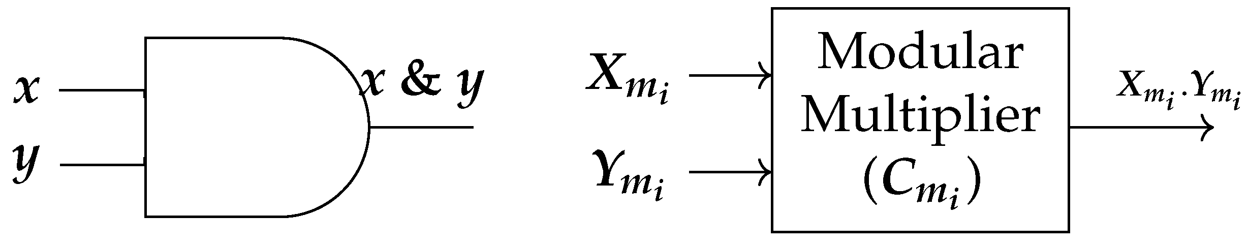
In RNS logic, binary operators, such as AND and XOR, are converted into their equivalent residue operators by combining the modulo multiplication and modulo addition to securely carry out the operation. An RNS gate equivalent to a Boolean AND gate is illustrated in Figure 2. The size of this circuit is not dependent on the number of shares, but rather on the modulus size (l).
The computation is replicated for the number of selected moduli shares. Each input vector participates in the computation unit for each modulus . The residue domain representation of the output Z is the linear congruence of the binary value z with respect to the modulus . To determine the final binary output bit, the Chinese remainder theorem (CRT) is used on the residue shares of the output from the RNS circuit.
Theorem 1
(Chinese remainder theorem). Let , where all the elements of M are pairwise co-prime. let , , …, be integers ∈℧. Then, the system of congruences, (mod ) for , has a unique solution modulo M = , which is given by:
where and (mod ) for .
Proof.
Notice that gcd(,) = 1 for . Therefore, the ’s all exist. Now, notice that, since (mod ), we have (mod ) for . On the other hand, (mod ) if . Thus, we see that (mod ) for . □
In order to use the Chinese remainder theorem, the modulus values used to create shares must be relatively prime to each other. To uncover the mask, the value e must be subtracted from the result of the CRT, followed by a mod 2 operation. In this example, the value e is calculated as .
SCA Characteristics
The RNS secure logic utilizes an encoding scheme that transforms all binary inputs into multiple residues with modulo-different co-prime moduli, as expressed in Equation (1). Many adversary models exist depending on the implementation. How many residues are visible to the adversary? Note that different residues could be computed on different chips or on the same chip in different power domains, or on the same chip in the same power domain. Each of these presents different complexities to the adversary. If the modulus is known, and the residue is in the open, the input bit is also known. A randomly generated number then helps conceal the binary value through the application of the modulo addition operation. In contrast to other side-channel countermeasures, the shares are produced by means of modular addition. This has the potential to uncover the connection between a residue and the related input bit by looking at the distributions of bits within the residue. Across the range of all hidden parameters, modulus , and random value , an input bit value of 0 is associated with a multitude of residues, denoted by . Similarly, an input bit of 1 is associated with a set of residues . It is desirable that the two sets and are indistinguishable to the adversary. This property, referred to as residue indistinguishability or symmetry, conceals the connection between the input and the residue.
where i varies from 1 to . r is a random value.
Symmetry is the probability that the adversary is unable to tell the difference between the input bit states based on the distribution of residue values. In a realistic attack, the adversary does not have access to the residue values, and instead makes an educated guess about the residue state through a power side-channel. Generally, these power models are based on the Hamming weight. Consequently, the main factor that distinguishes different residues is their Hamming weight difference. The adversary tries to learn the state of the input bit (0 or 1) by measuring slight variations in the average Hamming weight related to the residues of input bits 0 and 1. If the average Hamming weights are the same, there is perfect symmetry, which denies the adversary this information. Equation (2) demonstrates this concept for a fixed modulus value . The targeted chip is operational with a fixed , and thus the uncertainty for the adversary is generated by the random mask .
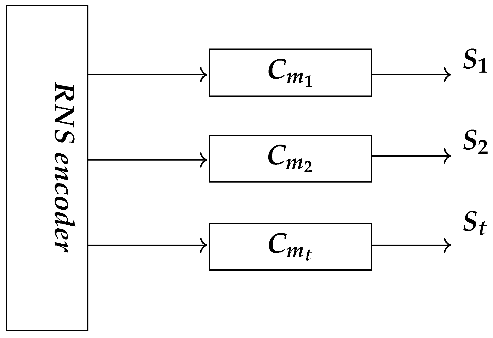
In addition to the residue indistinguishability property, the RNS logic has another interesting feature known as multi-lane computation, as shown in Figure 3. The RNS encoding produces encrypted shares that are congruent with each other with respect to the moduli . This allows the hardware designer to create separate hardware for each share. Each share computation can occur completely independently from the others, allowing for a variety of architectures to share across multiple power domains, or multiple chips, or multiple racks, or multiple cloud nodes-leading to increasing complexity for the adversary.
4. Security Analysis of PDN Topology
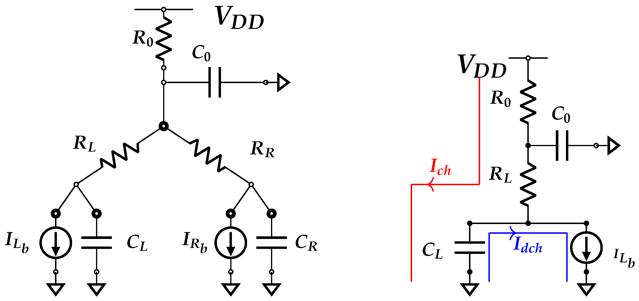
We discussed the power distribution network from the drop stability point of view. In this section, we focus on the PDN characteristics that are pertinent to side-channel analysis. As discussed in Section 3, the power distribution networks are depicted as an plane, with R and C representing the parasitic resistance and capacitance of the metal wires in the PDN design. The nodes of the logic blocks are leaves of the power distribution network. We illustrate the activities of the power distribution network with a single layer circuit, as shown in Figure 4. The current draw for the switching activity of the logic blocks and is represented by the nodes and . The resistance and capacitance of the left and right branches of the power grid, , , , and , are the parasitic components of the metal layer. The resistor and capacitor near the pin are the only components accessible to the adversary in power analysis attacks. The current drawn across the resistor is equivalent to the power leakage captured at by the adversary across the off-chip power network. According to Kirchoff’s current law, the current across the resistor is expressed in Equation (3).
The parasitic capacitances of the power grid , , and have a negligible effect on the overall power consumption. This causes the current to be equal to the sum of the current drawn by the circuits and .
We investigated the power side-channel characteristics of the PDN by assuming a sensitive circuit block that processes the secret data values and a non-sensitive circuit block that introduces noise to the power side-channel adversary. The adversary’s objective is to exploit the power-data correlation leakage that is caused by the switching activity of the internal logic block through the off-chip power supply network. The trace contains all the information needed to extract a certain feature vector, including peaks and time slopes. The peak is associated with the state of an internal circuit that experiences the most switching during computing. The peak values in the current trace differ depending on the amount of data-dependent charging and discharging of the transistors. Logic gates are designed to generate steady outputs within their allotted time frames, based on the clock. The scheduling specification permits the logic gates to switch at different times, which determines the maximum current and the rate of change in the current between successive stages (the current slope). The resistive path of the power distribution network only reduces/increases the magnitude of the current peak through the resistive spread, but the number of peaks stays the same regardless of the PDN parameters.
The decoupling capacitor based on CMOS technology is able to store enough charge to meet the current draw needs of the logic block for a short period of time. Even one clock cycle of switching activity charge on a decoupling capacitor can put off a power side-channel adversary. This capacitance allows the secret value-dependent circuit activity to be almost disconnected from the pin for some duration. During this phase, the capacitor charges or discharges the logic block . A minimal current is drawn from the pin, which has an impact on the transmission of feature vectors to the pin.
The cycle of charging and discharging of the decoupling capacitor is shown in Figure 4. When the circuit is powered on, the decoupling capacitor is charged quickly. This charge is then used to provide current to the logic cells. The power distribution network is constantly supplied through the pin as per the circuit’s specifications. The stability of the input power supply allows for a steady current flow in each branch of the power distribution network. When the demand for the switching current is greater than the constant branch current, i.e., > , the capacitor begins to discharge. The rate of discharge is determined by the switching activity level at the logic cell.
The amount of side-channel leakage is determined by the current demand at the node, which is caused by the propagation of the switching current . The discharge of the decoupling capacitance has a significant effect on the propagation of the current profile. This discharge cycle is data-dependent, and the current profile is similar to the switching current profile of the logic cell. Therefore, the branch current can be expressed as:
where is the time interval for decoupling the capacitance discharge cycle; and is voltage drop at the logic node .
At time , the logic block current is less than the branch current , causing the decoupling capacitance to switch to the charging cycle. During this period, the capacitor draws current from the pin to recharge at a steady rate. The total branch current is then:
where is the total time period of the charging cycle. is the total resistance of the path from to the logic block .
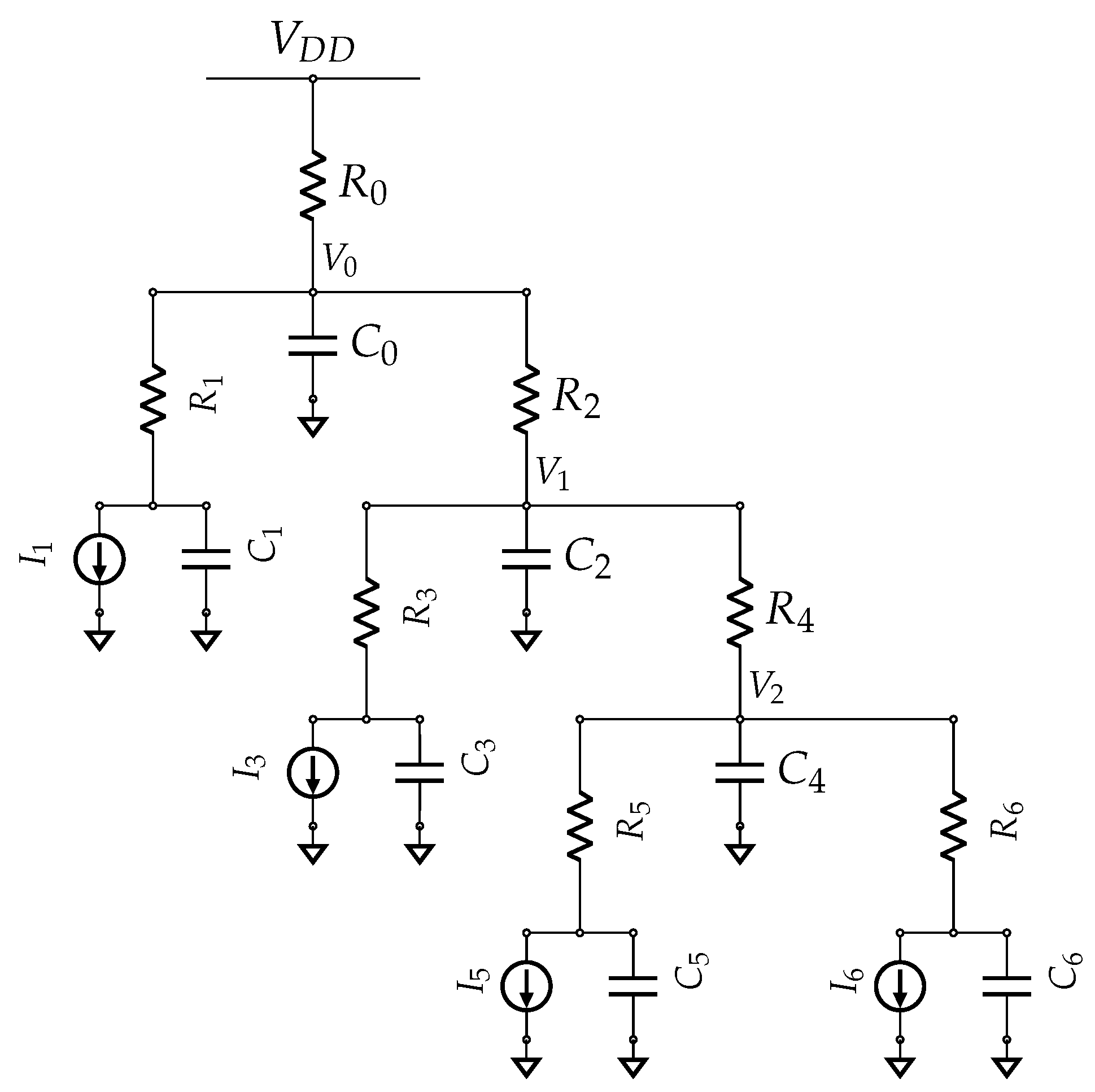
4.1. Modeling Tree-Style PDN Side-Channel Leakage
Traditionally, a PDN is designed to supply voltage to the logic nodes with minimal fluctuation so that the transistors operate at close to full swing voltage. There are two different PDN topologies that are more common in any CMOS circuit: (i) tree-style PDN; and (ii) grid-style PDN.
For tree-structured PDN, the order of the model k is proportional to the depth of tree-style PDN. Therefore, the depth of the tree plays a vital role in the propagation of data-dependent leakage. A higher order, degree of polynomial in the model, presents more challenges to a machine learning adversary. In order to estimate the degree or order of the model, we apply KCL techniques.
For depth 1:
In closed form solution, the transfer function at I1 is given by
where:
The closed form solution for depth 2 and depth 3 tree PDN can be computed the same way. The order or degree of the higher depth tree PDNs are shown in Table 1. For tree-style PDN, the order or degree of the model is proportional to the depth, as shown in Figure 5. Hence, the complexity of modeling the PDN increases with the depth of the logic block in a PDN. If the order is high, the side-channel adversary finds it difficult to model the propagation of data-dependent leakage to the external . Alternately, a machine learning technique needs a larger model to learn a higher-order PDN model. The higher model dimensionality leads to a larger feature space size to maintain the same accuracy.
4.2. Modeling Grid-Style PDN Side-Channel Leakage
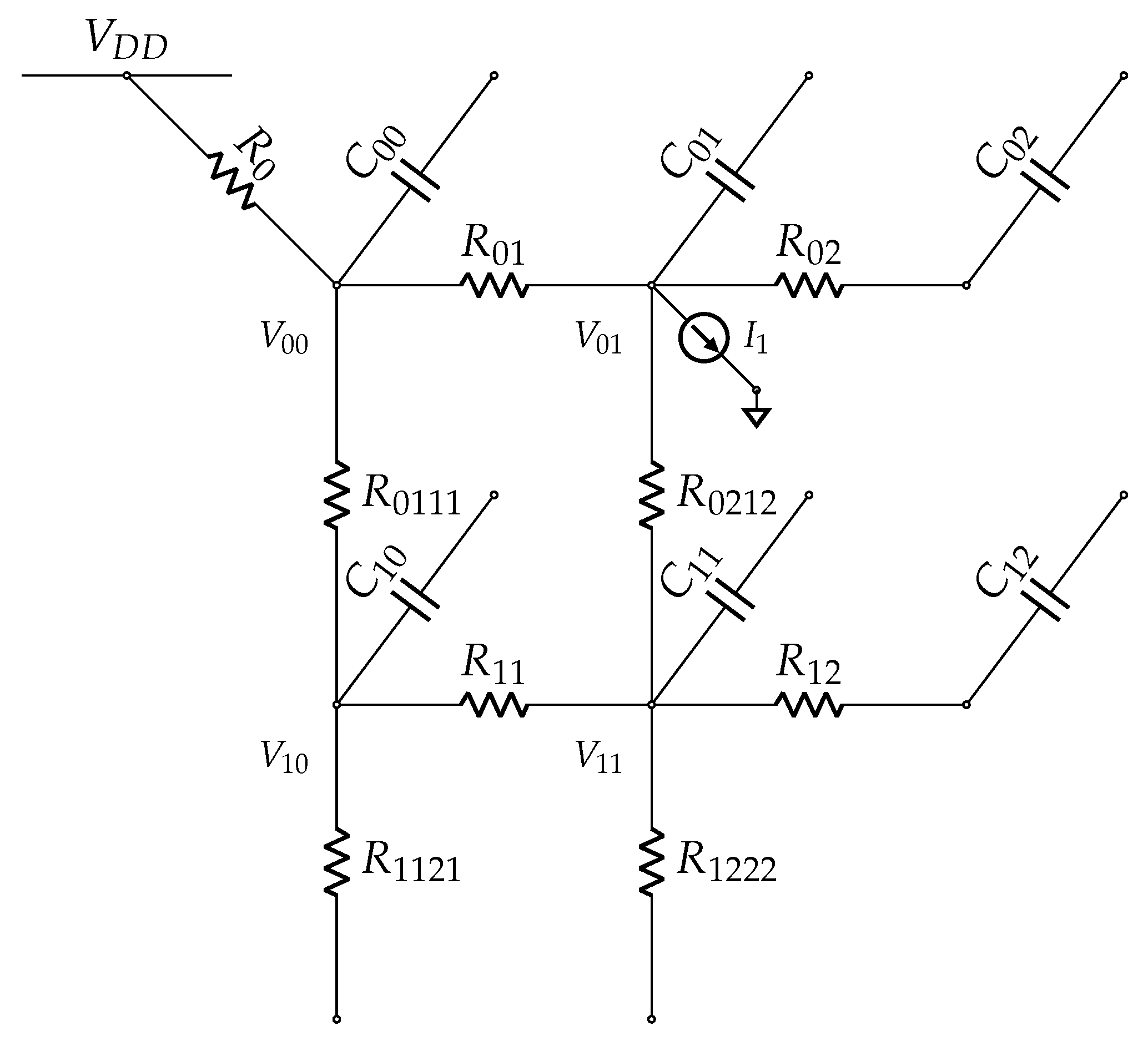
Unlike tree-style PDN, the grid structure closed-form model computation is not straightforward. The reason is that a logic block in the grid structure has multiple power paths to the external pin leading to a parallel RC network. There are specialized nodes in the grid-style PDN that completely block the voltage source from reaching the logic block, as shown in Figure 6. Such a combination of nodes is denoted as a “cut”. The size of the cut, the minimum number of edges that need to be cut to make the PDN graph disconnected with the critical logic block in one set, and pin in the other set, plays a role in determining the data-dependent leakage to the external . Once again, we apply KCL to build such a model.
The closed form solution of the power path from to is given by
where:
From Equation (9), it is clear that modeling data-dependent leakage that occurs at node requires an order 4 solution which is more complex compared to tree-style PDN. For a successful power side-channel attack against distributed decoupling capacitance, the adversary has to learn a model of the PDN with an order 7 model for the cut size 4. When comparing the order of two different topologies, it is evident that the grid-style PDN design reduces the side-channel leakage from the targeted logic block to the external pin.
5. Results and Discussion
In general, power side-channel countermeasures are designed to use random bits to mask the secret value or to generate noise to weaken side-channel leakage by making the computing signature more like white noise. To date, all SCA countermeasure techniques have been individually investigated for side-channel resistance. RNS secure logic is a logic level technique that encrypts input data with the RNS input encoder to create multiple residue shares of each input bit. The residue domain gates process these input bits into an output result residue, which can then be converted back into Boolean domain with CRT. PDN with the decoupling capacitance decouples the logic node for a short time to obfuscate the propagation of side-channel leakage reaching the external pin. One of the goals of this paper is to evaluate whether these two techniques from logic level and physical level were integrated together, would the side-channel mitigation be better than if only one of them were used. In other words, if these techniques are orthogonal and additive. The more general question is that of whether the side-channel mitigation techniques at different design flow abstraction levels are likely to be orthogonal and additive.
The second important question addressed in this paper is the relative evaluation of different PDN topologies, specifically tree and grid PDNs, with respect to power side-channel leakage. We have already developed a KCL-based model for side-channel leakage for a PDN in Section 4. The order or degree of this model provides us with the side-channel leakage suppression capabilities of two PDNs. The higher the order of the model, the higher the side-channel leakage resistance. This model does not provide an absolute measure of the power side-channel resistance. We perform a machine learning-based evaluation of the side-channel leakage of the tree PDN and grid PDN topologies for a 64-bit block encryption LED algorithm [41].
5.1. Experiment
In RNS secure logic, high-level masking is applied using a homomorphic encryption technique. Furthermore, the RNS secure circuit ensures strong cryptographic privacy and side-channel privacy through the symmetry and switching properties. The power profile of the RNS secure circuit may be the same for different secret values due to the symmetric residue value. However, the transition probability of the residue share in the RNS secure circuit is biased towards the most significant bit of the residue values. This may open an opportunity for an adversary to mount a side-channel attack. The combined side-channel resistance of the RNS secure logic with the decoupling capacitance and security-aware PDN may overcome such potential vulnerabilities.
The LED algorithm, a 64-bit block encryption algorithm with a 64-bit key, is evaluated for side-channel leakage. Specifically, the S-box is the targeted stage for the secret data leakage. All the other algorithm stages AddRoundKey, AddConstant, and MixColumn, are considered as other logic blocks adding noise.
5.1.1. RNS Implementation
The RNS secure logic of the LED-64 round function is implemented using the NCSU FreePDK 45 nm technology library in Cadence Virtuoso. LED-64 is one of the symmetric key light-weight algorithms which uses a 64-bit secret key. Each round of LED-64 has four operations; S-box (SB), AddRoundKey (ARK), AddRoundConstants (ARC), and MixColumn (MXC). Each of these operations corresponds to a functional block. The RNS schema uses 3-bit moduli and random values. A 3-bit random value is used only in the input encoder. Note that there are many variations of RNS schema with a variable use of random variables. A higher number of random variables results in higher side-channel resistance. The input encoder random variable use is the minimal schema with the lowest side-channel resistance compared to the base design.
5.1.2. PDN Implementation
A tree-style PDN is constructed with a depth of 3 for the RNS-protected LED round functions. For all of our experiments, each functional block has separate inputs for the computation, and the outputs are connected to a fixed load capacitance of 0.5 . In this work, the adversary’s goal is to infer the secret data values from the feature vectors extracted from the voltage drop and the switching current caused by the circuits’ transitions on the power distribution network. The S-box function is considered to be a critical targeted function in any encryption for side-channel analysis; for this reason, the S-box function (SB) is assumed to be a target function for an adversary. Each branch of the power tree is constructed with parasitic resistance R and capacitance C.
For this experiment, the decoupling capacitance was selected in the range of 1.20–60 pico-farads. The capacitance was evenly spread out at the points where the power distribution network (PDN) branches off. The presence of a decoupling capacitance significantly reduces the transmission of the feature vector and makes it less visible at the external pin. This hinders the adversary’s capacity to create a model and thus protects the secret data from being revealed.
The distribution of the decoupling capacitance along the power tree provides a momentary supply of power to the logic block node and reduces the visibility of the feature vector at . In comparison to the single-capacitance model, the current draw of other logic block junctions with multiple capacitances is more complex and unpredictable. This makes it more difficult for an adversary to succeed in their attempts. To further confuse the adversary, a randomized decoupling schedule can be activated, which assigns a fixed capacitance value to the power path. We evaluated such randomized decoupling schedules in this experiment.
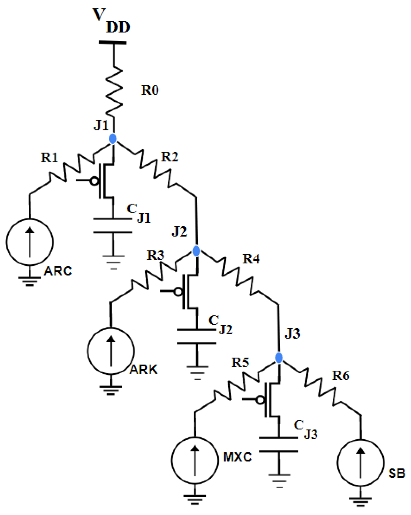
In tree-style PDN, the decoupling capacitance is placed at the junction along the power path from the logic node to , as shown in Figure 7. There are three decoupling capacitances placed at junction nodes , , and with the same capacitance value. For each input vector, a random value is generated to randomly enable PMOS switches to connect any two decoupling capacitances in the power tree. The total capacitance on the power path that is activated is referred to as , and the ML results related to this are presented in Table 2. A similar setting is applied for the RNS-protected LED functional block, and the success rate of the ML adversary is given in Table 3. The maximum decoupling capacitance for the LED functional block and its RNS secure logic is 12 and 60 , respectively. The decoupling capacitance for the LED functional block is limited to 12 due to the complexity of the simulation time, while the decoupling capacitance for the LED-RNS secure logic is increased to 60 due to the increased current demand at the logic nodes. The success rate for the highest values of the 60 decoupling capacitor is 13%, which is a reduction of 84% compared to the unprotected circuit.
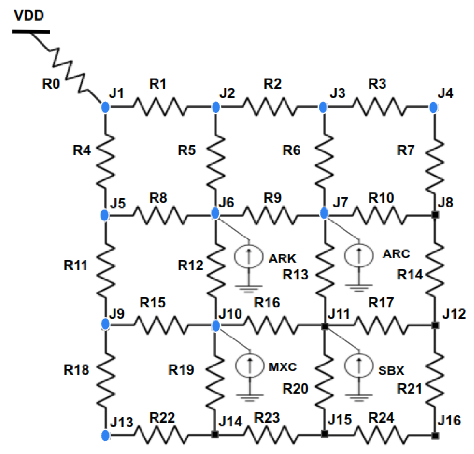
A grid-style power distribution network (PDN) is arranged with logic blocks in a grid pattern, with each junction providing and ground. This structure is more resilient and has less noise than the power tree. We constructed a 4 × 4 power grid with a route resistance of 1 to analyze the side-channel resistance for this PDN, as shown in Figure 8. The junction nodes J6, J7, J10, and J11 are linked to the AddRoundKey (ARK), AddConstant (ARC), MixColumn (MXC), and S-box (SB) functional blocks, respectively.
The decoupling capacitance is placed at the junction to cut off the power path between the logic node and . Ten decoupling capacitances are placed along with PMOS switches at the junction nodes of the power path that connect the logic blocks, which are shown in Figure 8 with the same capacitance value. For each input vector, a random value is generated to activate four decoupling capacitances in the power grid. The success rate of the ML adversary for the LED functional block and RNS protected circuits are given in Table 4 and Table 5. The success rate for the highest values of the 60 decoupling capacitor is approximately 10%, which is a reduction of 88% compared to the unprotected circuit.
5.2. Machine Learning for Side-Channel Leakage
All experiments were carried out using 10,000 randomly generated inputs. Four different machine learning classifiers were used—naive Bayes (NB), linear discriminant analysis (LDA), quadratic discriminant analysis (QDA), and support vector machine (SVM). In order to train machine learning classifiers, feature vectors are created with the peak voltage and current values observed on the pins. These feature vectors are labeled with secret data values, which are the input values of the S box. The success rate of the ML adversary is higher when the power distribution network transmits the power feature vector from the RNS secure S-box to the node without any suppression; however, if the leakage is suppressed by the decoupling capacitors or other methods, the success rate of the ML adversary is lower.
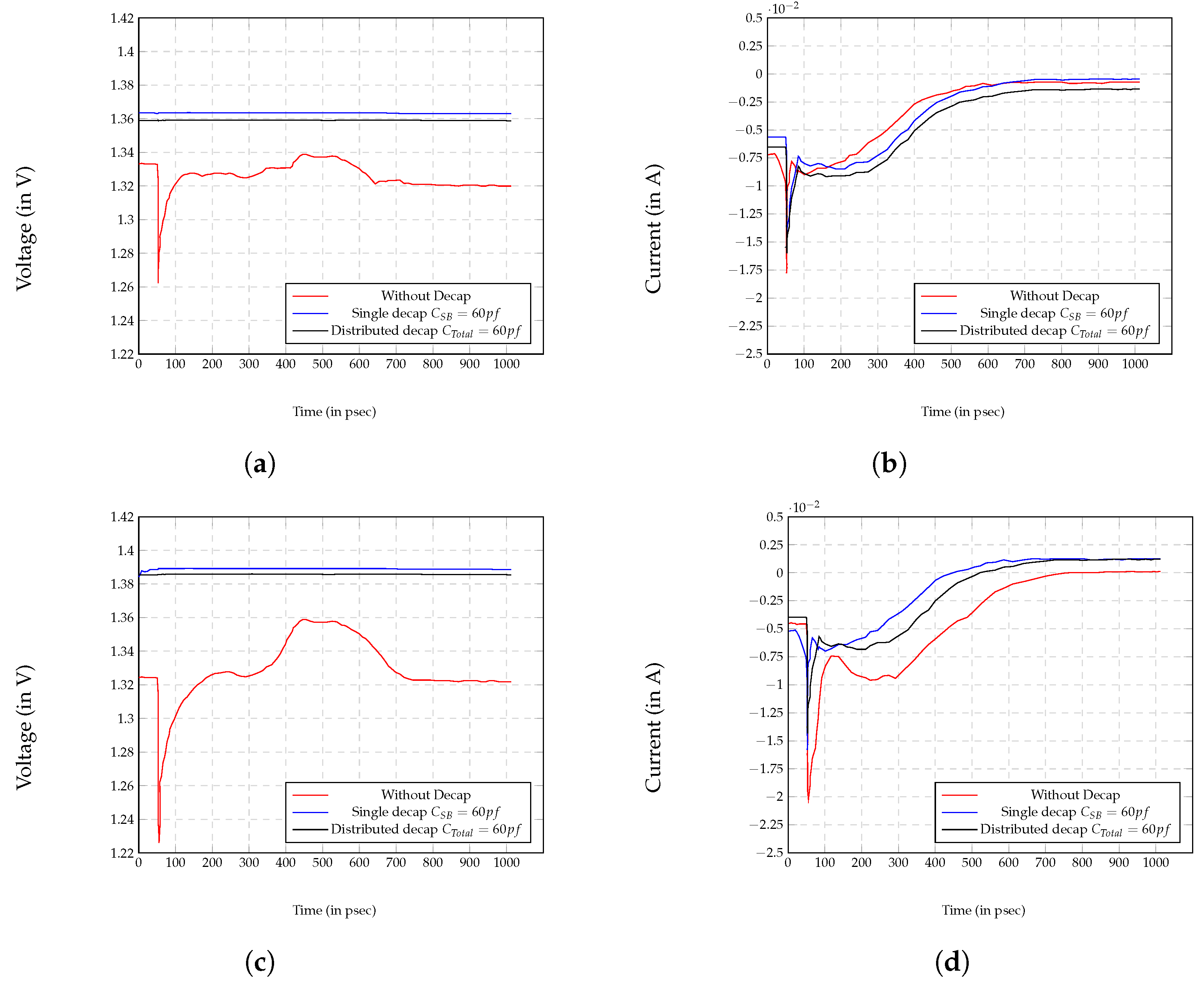
An adversary utilizing a power analysis attack can constantly monitor the pin for the model feature vectors created from the switching current of the sensitive logic block. The charge/discharge cycle of the decoupling capacitance has a major impact on the peak and slope seen at the pin. As shown in Figure 9, the power tree’s sensitivity to the decoupling capacitance is evident. The voltage signal with the 60 single lumped capacitance for a tree PDN (Figure 9c) shows a slight jitter at the beginning for 30–50 ps. In all other cases, with the distributed 60 pf capacitance, it is a flat profile. For grid PDN, the voltage signal (Figure 9a) is always flat. This is in contrast to the voltage signal without a decoupling capacitance which shows a significant amount of variance, potentially revealing sensitive information. For the current profile, both tree PDN and grid PDN show significant variation—the tree PDN has a slightly higher variation than the grid PDN with no decoupling capacitance. For the tree PDN (Figure 9d), both lumped and distributed capacitance values of 60 pf moderate this variation significantly, and distributed capacitance a little more. Similarly, in grid PDN (Figure 9b), the same pattern holds. The initial valley at about 50 ps is suppressed a bit more for grid PDN than in the tree PDN. Again, the distributed capacitance performs slightly better, but less so than in the tree PDN case. The decoupling capacitance during the discharge cycle reduces the peak current values in its branch. Furthermore, the peak value traveling through the power distribution network increases the switching noise from other logic cells. This switching noise makes the characteristics observed at the pin difficult to exploit by an adversary.
5.3. Results
Row 1 of Table 2 shows the base LED implementation without any decoupling capacitance on the tree PDN-neither of the RNS logic or decoupling capacitance PDN protections is applied. The success rate of SVM on this base case is 88.31%. Similarly, Row 1 of Table 4 shows the base LED implementation without any decoupling capacitance on grid PDN. The success rate of SVM on this base case is 66.58%. This demonstrates the base advantage of grid PDN over the tree PDN.
Comparing Rows 2–5 of Table 2 and Table 4 corresponding to decoupling capacitances of 1.2 , 3.6 , 6 , and 12 , respectively, for tree PDN and grid PDN. In almost all of these cases, the SVM success rate goes down, 53.43% → 52.68% for 1.2 case, again confirming the superiority of grid PDN over tree PDN in suppressing side-channel leakage.
Consider the Rows 1–5 of Table 2 where the decoupling capacitance in a tree PDN progressively increases from 0 to 12 . The success rate goes down progressively from 88.31% to 15.72% illustrating the effectiveness of decoupling capacitance as a side-channel mitigation technique. The same trend holds for grid PDN (Table 4) where SVM success rate goes down from 66.58% to 13.49%.
Now, let us look at Table 3 for tree PDN with RNS logic. Compare the SVM success rates against Table 2 for the tree PDN without RNS logic. As Table 6 shows, the RNS logic implementation takes roughly twice the area of the base LED implementation. This would imply that roughly double the switched capacitance will occur in the RNS LED logic blocks than in the base LED logic blocks. This means that a decoupling capacitance of C in the base LED implementation would have the same effect on the ML success rate as 2*C decoupling capacitance in RNS LED implementation. A corresponding switching event in RNS LED will need twice the amount of charge for the same event in base LED. In practice, the results in Table 2 show that the effective switched capacitance in the RNS LED compared to the base LED is five times larger. Hence, for example, the 12 row of Table 2 should be compared against the 60 row of Table 3. This does show an SVM success rate improvement from 15.72% to 13.15%.
Similarly, for the grid PDN, let us compare Table 4 and Table 5. Once again, the 12 row of Table 4 is comparable to the 60 row of Table 5. It shows a success rate improvement from 13.49% to 10.54%.
Overall, these results do confirm that the two side-channel mitigation techniques, one at the logic level and the other at the physical level, are orthogonal and additive.
5.4. Discussion
Let us first start with the area comparison of RNS LED and base LED implementations. The area overhead is given in Table 6. In this scenario, the RNS-protected LED round function area overhead is approximately 2.5 times compared to the base LED round function. The decoupling capacitors cost the additional area. The area of silicon occupied by the decoupling capacitance is 118.12 um for a capacitance of 2 .
We expect the decoupling capacitance values up to the load capacitances of the targeted logic block to show a decrease in the success rate. The decoupling capacitor would be able to hide the switching pattern from the pin adversary up to that point. We limited our experiments to decoupling capacitance values approximately up to 30% of the logic block load capacitance. Even though the ML adversary success rate continuously decreases, the decoupling capacitance value for the LED functional block is limited to 12 due to the complexity of the simulation time. Similarly, the decoupling capacitance value for the LED-RNS secure circuit is evaluated at 60 . The upper limit of the decoupling capacitance for the RNS-protected LED circuit is increased because of the increased current demand at the logic node. The RNS-protected LED functional logic increases the area and power by approximately 200% compared to the base LED functional logic block.
6. Conclusions
In this paper, we raised two questions. One was concerned with the orthogonality of the power side-channel mitigation techniques at different design abstraction levels. We set out to assess the orthogonality of the RNS secure logic at the logic level with the decoupling capacitance PDN at the physical level. As our results show, the effectiveness of an LED block cipher combining both mitigation techniques is higher than with only either one of the techniques. The validation of the broader question would require further research into a broader set of power side-channel mitigation techniques. A quick resolution of the potential feature vectors’ orthogonality from different abstraction levels would be a useful design tool in answering such questions.
The second question answered by this paper is the comparison of two PDN topologies, tree and grid, with respect to power side-channel mitigation. We showed that grid PDN almost always performs better—in terms of an abstract feature vector propagation analysis, in terms of an implementation’s ML success rate, and in terms of an analytical model based on KCL. The KCL-based model, whose degree is a strong indicator of the power side-channel mitigation potential, is a useful back of the envelope analysis tool for comparing two different PDN topologies. It is a significant contribution in itself.
Many other interesting research questions remain in this domain. Are there synergies between placement and PDN design? Could dynamically shifting placements in a reconfigurable fabric offer a good mitigation technique? Could these decoupling capacitances be repurposed out of existing blocks whose active schedules are disjoint from the target block so that the target block charge could be sourced partially from the inactive logic blocks? We are looking into these research questions.
Author Contributions
A.T. and R.S. conceived, designed the experiments and wrote the paper; R.S. performed the experiments and analyzed the data. All authors have read and agreed to the published version of the manuscript.
Funding
This research received no external funding.
Data Availability Statement
Data are contained within the article.
Conflicts of Interest
The authors declare no conflict of interest.
Abbreviations
The following abbreviations are used in this manuscript:
| ASL | All-Spin Logic |
| CPA | Correlation Power Analysis |
| CRT | Chinese Remainder Theorem |
| DPA | Differential Power Analysis |
| FPGA | Field Programmable Gate Array |
| GE | Gate Equivalence |
| HO-SCA | Higher-Order Side-Channel Attack |
| HOA | Higher-Order Attacks |
| IoT | Internet of Things |
| KL Divergence | Kullback–Leibler Divergence |
| LDA | Linear Discriminant Analysis |
| ML | Machine Learning |
| NB | Naive Bayes |
| NCSU | North Carolina State University |
| PDN | Power Distribution Network |
| QDA | Quadratic Discriminant Analysis |
| RNS | Residue Number System |
| RRAM | Resistive Random Access Memory |
| SABL | Sense Amplifier-Based Logic |
| SCA | Side-Channel Attack |
| SiNWFETs | Silicon Nanowire FETs |
| SVM | Support Vector Machine |
| WDDL | Wave Dynamic Differential Logic |
References
- Kocher, P.C.; Jaffe, J.; Jun, B. Differential power analysis. In Proceedings of the Advances in Cryptology-CRYPTO ’99, 19th Annual International Cryptology Conference, Santa Barbara, CA, USA, 15–19 August 1999; pp. 388–397. [Google Scholar]
- Kocher, P.C. Timing attacks on implementations of diffie-hellman, rsa, dss, and other systems. In Proceedings of the Advances in Cryptology—CRYPTO ’96, Santa Barbara, CA, USA, 18–22 August 1996; Koblitz, N., Ed.; Springer: Berlin/Heidelberg, Germany, 1996; pp. 104–113. [Google Scholar]
- Quisquater, J.J.; Samyde, D. Electromagnetic analysis (ema): Measures and counter-measures for smart cards. In Proceedings of the International Conference on Research in Smart Cards, Cannes, France, 19–21 September 2001; Springer: Berlin/Heidelberg, Germany, 2001; pp. 200–210. [Google Scholar]
- Genkin, D.; Pipman, I.; Tromer, E. Get your hands off my laptop: Physical side-channel key-extraction attacks on pcs. In Proceedings of the Cryptographic Hardware and Embedded Systems—CHES 2014, Busan, Republic of Korea, 23–26 September 2014; Batina, L., Robshaw, M., Eds.; Springer: Berlin/Heidelberg, Germany, 2014; pp. 242–260. [Google Scholar]
- Zhou, Y.; Feng, D. Side-Channel Attacks: Ten Years after Its Publication and the Impacts on Cryptographic Module Security Testing. 2005. Available online: http://eprint.iacr.org/2005/388 (accessed on 2 December 2023).
- Chari, S.; Rao, J.R.; Rohatgi, P. Template attacks. In Proceedings of the Cryptographic Hardware and Embedded Systems-CHES 2002, 4th International Workshop, Redwood Shores, CA, USA, 13–15 August 2002; pp. 13–28. [Google Scholar]
- Moradi, A.; Mischke, O.; Eisenbarth, T. Correlation-enhanced power analysis collision attack. In Proceedings of the Cryptographic Hardware and Embedded Systems, CHES 2010, 12th International Workshop, Santa Barbara, CA, USA, 17–20 August 2010; pp. 125–139. [Google Scholar]
- Shannon, C. A mathematical theory of cryptography. In Memorandum MM 45-110-02; Classified Report; Evervault: Dublin, Ireland, 1945. [Google Scholar]
- Goldreich, O.; Goldwasser, S.; Micali, S. How to construct random functions. J. ACM 1986, 33, 792–807. [Google Scholar] [CrossRef]
- Conti, M.; Losiouk, E.; Poovendran, R.; Spolaor, R. Side-channel attacks on mobile and iot devices for cyber–physical systems. Comput. Netw. 2022, 207, 108858. [Google Scholar] [CrossRef]
- Zhao, M.; Suh, G.E. FPGA-Based Remote Power Side-Channel Attacks. In Proceedings of the IEEE Symposium on Security and Privacy (SP), San Francisco, CA, USA, 21–23 May 2018; pp. 229–244. [Google Scholar]
- Randolph, M.; Diehl, W. Power Side-Channel Attack Analysis: A Review of 20 Years of Study for the Layman. Cryptography 2020, 4, 15. [Google Scholar] [CrossRef]
- Shamir, A. How to share a secret. Commun. ACM 1979, 22, 612–613. [Google Scholar] [CrossRef]
- Ishai, Y.; Sahai, A.; Wagner, D.A. Private circuits: Securing hardware against probing attacks. In Proceedings of the Advances in Cryptology, 23rd Annual International Cryptology Conference (CRYPTO 2003), Santa Barbara, CA, USA, 17–21 August 2003; Boneh, D., Ed.; Springer: Berlin/Heidelberg, Germany, 2003; Volume 2729, pp. 463–481. [Google Scholar]
- Bucci, M.; Giancane, L.; Luzzi, R.; Trifiletti, A. Three-phase dual-rail pre-charge logic. In Proceedings of the Cryptographic Hardware and Embedded Systems, 8th International Workshop (CHES 2006), Yokohama, Japan, 10–13 October 2006; Goubin, L., Matsui, M., Eds.; Springer: Berlin/Heidelberg, Germany, 2006; Volume 4249, pp. 232–241. [Google Scholar]
- Tiri, K.; Verbauwhede, I. Design method for constant power consumption of differential logic circuits. In Proceedings of the Conference on Design, Automation and Test in Europe, Munich, Germany, 7–11 March 2005. [Google Scholar]
- Guilley, S.; Chaudhuri, S.; Sauvage, L.; Graba, T.; Danger, J.; Hoogvorst, P.; Vong, V.; Nassar, M.; Flament, F. Shall We Trust WDDL? Vieweg + Teubner: Wiesbaden, Germany, 2009; pp. 208–215. [Google Scholar]
- Alasad, Q.; Yuan, J.; Lin, J. Resilient aes against side-channel attack using all-spin logic. In Proceedings of the 2018 on Great Lakes Symposium on VLSI, GLSVLSI ’18, Chicago, IL, USA, 23–28 May 2018; Association for Computing Machinery: New York, NY, USA, 2018; pp. 57–62. [Google Scholar]
- Khedkar, G.; Donahue, C.; Kudithipudi, D. Towards leakage resiliency: Memristor-based AES design for differential power attack mitigation. In Machine Intelligence and Bio-Inspired Computation: Theory and Applications VIII; Blowers, M., Williams, J., Eds.; International Society for Optics and Photonics, SPIE: Cergy-Pontoise, France, 2014; Volume 9119, p. 911907. [Google Scholar]
- Giacomin, E.; Gaillardon, P.E. Differential power analysis mitigation technique using three-independent-gate field effect transistors. In Proceedings of the 2018 IFIP/IEEE International Conference on Very Large Scale Integration (VLSI-SoC), Verona, Italy, 8–10 October 2018; pp. 107–112. [Google Scholar]
- Selvam, R.; Tyagi, A. Power Side Channel Resistance of RNS Secure Logic. In Proceedings of the 2018 31st International Conference On VLSI Design and 2018 17th International Conference On Embedded Systems (VLSID), Pune, India, 8–10 January 2018; pp. 143–148. [Google Scholar]
- Selvam, R.; Tyagi, A. An Evaluation of Power Side-Channel Resistance for RNS Secure Logic. Sensors 2022, 22, 2242. [Google Scholar] [CrossRef] [PubMed]
- Selvam, R.; Tyagi, A. Power distribution network capacitive decoupling for side-channel resistance. In Proceedings of the 2021 IEEE International Symposium on Smart Electronic Systems (iSES), Jaipur, India, 18–22 December 2021; pp. 183–188. [Google Scholar]
- Tang, K.T.; Friedman, E.G. Transient ir voltage drops in cmos-based power distribution networks. In Proceedings of the 43rd IEEE Midwest Symposium on Circuits and Systems (Cat.No.CH37144), Lansing, MI, USA, 8–11 August 2000; Volume 3, pp. 1396–1399. [Google Scholar]
- Mao, J.; Kim, W.; Choi, S.; Swaminathan, M.; Libous, J.; O’connor, D. Electromagnetic modelling of switching noise in on-chip power distribution networks. In Proceedings of the 8th International Conference on Electromagnetic Interference and Compatibility, Chenai, India, 18–19 December 2003; pp. 47–52. [Google Scholar]
- Tanaka, H.; Matsushima, T.; Yano, Y.; Wada, O. Compensating method of equivalent current sources of lsi-core macromodel considering voltage fluctuations in on-chip power distribution network. IEEE Trans. Electromagn. Compat. 2022, 64, 1250–1256. [Google Scholar] [CrossRef]
- Tang, K.T.; Friedman, E.G. Simultaneous switching noise in on-chip cmos power distribution networks. IEEE Trans. Very Large Scale Integr. Syst. 2002, 10, 487–493. [Google Scholar] [CrossRef]
- Joo, J.; Sun, Y.; Lee, J.; Kong, S.; Kang, S.; Song, I.; Hwang, C. Modeling of power supply noise associated with package parasitics in an on-chip ldo regulator. In Proceedings of the 2021 IEEE International Joint EMC/SI/PI and EMC Europe Symposium, Raleigh, NC, USA, 26 July–13 August 2021; pp. 395–399. [Google Scholar]
- Mayhew, M.; Muresan, R. Modeling the effect of nmos gate capacitance in an on-chip decoupling capacitor paa countermeasure. In Proceedings of the 2014 IEEE 57th International Midwest Symposium on Circuits and Systems (MWSCAS), College Station, TX, USA, 3–6 August 2014; pp. 121–124. [Google Scholar]
- Mayhew, M.; Muresan, R. On-chip nanoscale capacitor decoupling architectures for hardware security. IEEE Trans. Emerg. Top. Comput. 2014, 2, 4–15. [Google Scholar] [CrossRef]
- Dofe, J.; Yu, Q. Exploiting PDN noise to thwart correlation power analysis attacks in 3d ics. In Proceedings of the 20th System Level Interconnect Prediction Workshop, SLIP@DAC 2018, San Francisco, CA, USA, 23 June 2018; pp. 6:1–6:6. [Google Scholar]
- Kenarangi, F.; Partin-Vaisband, I. Exploiting machine learning against on-chip power analysis attacks: Tradeoffs and design considerations. IEEE Trans. Circuits Syst. Regul. Pap. 2019, 66, 769–781. [Google Scholar] [CrossRef]
- Muresan, R. On-chip cmos self-decoupling battery cell system for security protection. Can. J. Electr. Comput. Eng. 2020, 43, 83–91. [Google Scholar] [CrossRef]
- Messerges, T.S. Using second-order power analysis to attack DPA resistant software. In Proceedings of the Cryptographic Hardware and Embedded Systems, Second International Workshop (CHES 2000), Worcester, MA, USA, 17–18 August 2000; Koç, Ç.K., Paar, C., Eds.; Springer: Berlin/Heidelberg, Germany, 2000; Volume 1965, pp. 238–251. [Google Scholar]
- Mangard, S.; Popp, T.; Gammel, B.M. Side-channel leakage of masked CMOS gates. In Proceedings of the Topics in Cryptology, Cryptographers’ Track at the RSA Conference 2005 (CT-RSA 2005), San Francisco, CA, USA, 14–18 February 2005; Menezes, A., Ed.; Springer: Berlin/Heidelberg, Germany, 2005; Volume 3376, pp. 351–365. [Google Scholar]
- Goddard, Z.N.; LaJeunesse, N.; Eisenbarth, T. Power analysis of the t-private logic style for fpgas. In Proceedings of the International Symposium on Hardware Oriented Security and Trust (HOST 2015), Washington, DC, USA, 5–7 May 2015; IEEE Computer Society: Washington, DC, USA, 2015; pp. 68–71. [Google Scholar]
- Moradi, A. Statistical tools flavor side-channel collision attacks. In Proceedings of the Advances in Cryptology, 31st Annual International Conference on the Theory and Applications of Cryptographic Techniques (EUROCRYPT 2012), Cambridge, UK, 15–19 April 2012; Pointcheval, D., Johansson, T., Eds.; Springer: Berlin/Heidelberg, Germany, 2012; Volume 7237, pp. 428–445. [Google Scholar]
- Nikova, S.; Rechberger, C.; Rijmen, V. Threshold implementations against side-channel attacks and glitches. In Proceedings of the Information and Communications Security, Proceedings of the 8th International Conference (ICICS 2006), Raleigh, NC, USA, 4–7 December 2006; Ning, P., Qing, S., Li, N., Eds.; Springer: Berlin/Heidelberg, Germany, 2006; Volume 4307, pp. 529–545. [Google Scholar]
- Takarabt, S.; Bahrami, J.; Ebrahimabadi, M.; Guilley, S.; Karimi, N. Security Order of Gate-Level Masking Schemes. In Proceedings of the 2023 IEEE International Symposium On Hardware Oriented Security Furthermore, Trust (HOST), San Jose, CA, USA, 1–4 May 2019; pp. 57–67. [Google Scholar]
- Ming, J.; Zhou, Y.; Cheng, W.; Li, H. Optimizing Higher-Order Correlation Analysis Against Inner Product Masking Scheme. IEEE Trans. Inf. Forens. Secur. 2022, 17, 3555–3568. [Google Scholar] [CrossRef]
- Guo, J.; Peyrin, T.; Poschmann, A.; Robshaw, M. The LED Block Cipher. In Proceedings of the Cryptographic Hardware and Embedded Systems—CHES 2011, Nara, Japan, 28 September–1 October 2011; Preneel, B., Takagi, T., Eds.; Lecture Notes in Computer Science. Springer: Berlin/Heidelberg, Germany, 2011; Volume 6917. [Google Scholar] [CrossRef]
Figure 1.
Power distribution network.

Figure 2.
RNS circuit AND.

Figure 3.
RNS secure circuit’s multi-lane computation.

Figure 4.
Switching current propagation.

Figure 5.
Tree-style power distribution network with depth 3.

Figure 6.
Grid-style power distribution network for cut 1.

Figure 7.
Tree-style PDN with pMOS-enabled decoupling capacitance.

Figure 8.
Grid-style PDN with pMOS-enabled decoupling capacitances.

Figure 9.
Extraction of feature vectors: (a) voltage drop in grid-style PDN; (b) switching current in grid-style PDN; (c) voltage drop in tree-style PDN; and (d) switching current in tree-style PDN.
Figure 9.
Extraction of feature vectors: (a) voltage drop in grid-style PDN; (b) switching current in grid-style PDN; (c) voltage drop in tree-style PDN; and (d) switching current in tree-style PDN.


Table 1.
Closed form analysis of PDN topology.
| PDN Topology | Cut/Depth | Order |
|---|---|---|
| Tree-Style PDN | 1 | 2 |
| 2 | 3 | |
| 3 | 4 | |
| Grid-Style PDN | 1 | 4 |
| 2 | 5 | |
| 3 | 6 | |
| 4 | 7 |
Table 2.
ML success rate of LED with tree-style PDN.
| NB | LDA | QDA | SVM | |
|---|---|---|---|---|
| 0 pf | 86.17% | 83.95% | 84.72% | 88.31% |
| 1.20 pf | 51.56% | 52.31% | 52.98% | 53.43% |
| 3.60 pf | 38.29% | 37.14% | 38.06% | 33.28% |
| 6.00 pf | 29.73% | 29.56% | 27.32% | 22.75% |
| 12.00 pf | 20.91% | 21.71% | 20.38% | 15.72% |
Table 3.
ML success rate of hybrid scheme with tree-style PDN.
| NB | LDA | QDA | SVM | |
|---|---|---|---|---|
| 0 pf | 59.23% | 58.94% | 61.27% | 54.63% |
| 1.20 pf | 65.41% | 64.06% | 64.52% | 55.19% |
| 3.60 pf | 65.89% | 63.11% | 63.86% | 54.75% |
| 6.00 pf | 59.37% | 59.38% | 58.92% | 53.05% |
| 12.00 pf | 50.67% | 51.22% | 52.71% | 47.96% |
| 24.00 pf | 40.34% | 42.73% | 42.98% | 35.27% |
| 36.00 pf | 31.56% | 33.24% | 32.57% | 22.43% |
| 60.00 pf | 20.15% | 21.67% | 21.50% | 13.15% |
Table 4.
ML success rate of LED with grid-style PDN.
| NB | LDA | QDA | SVM | |
|---|---|---|---|---|
| 0 pf | 68.96% | 67.44% | 67.51% | 66.58% |
| 1.20 pf | 48.73% | 51.06% | 51.13% | 52.68% |
| 3.60 pf | 39.67% | 40.67% | 40.85% | 43.46% |
| 6.00 pf | 19.25% | 21.38% | 21.46% | 19.07% |
| 12.00 pf | 16.04% | 17.43% | 15.34% | 13.49% |
Table 5.
ML success rate of hybrid scheme with grid-style PDN.
| NB | LDA | QDA | SVM | |
|---|---|---|---|---|
| 0 pf | 54.68% | 55.25% | 54.97% | 51.02% |
| 1.20 pf | 51.86% | 52.07% | 52.12% | 46.67% |
| 3.60 pf | 48.41% | 48.63% | 47.46% | 37.32% |
| 6.00 pf | 44.38% | 43.91% | 44.87% | 30.14% |
| 12.00 pf | 39.46% | 39.17% | 39.25% | 25.91% |
| 24.00 pf | 31.09% | 31.42% | 30.14% | 16.89% |
| 36.00 pf | 26.23% | 26.97% | 27.55% | 13.06% |
| 60.00 pf | 19.68% | 19.62% | 19.10% | 10.54% |
Table 6.
Area estimation of LED block cipher.
| Without RNS | With RNS | |||||
|---|---|---|---|---|---|---|
| Logic | Gate | Cell | Area (um) | Gate | Cell | Area (um) |
| S-box | 488 | 592 | 1374.10 | 1032 | 1244 | 3320.10 |
| MixColumn | 389 | 284 | 1096.30 | 859 | 587 | 2304.64 |
| AddRoundKey + AddConstant | 192 | 128 | 540.60 | 428 | 361 | 1132.38 |
| Total (w/o decoupling capacitance) | 1069 | 1004 | 3011.00 | 2319 | 2192 | 6757.12 |
Disclaimer/Publisher’s Note: The statements, opinions and data contained in all publications are solely those of the individual author(s) and contributor(s) and not of MDPI and/or the editor(s). MDPI and/or the editor(s) disclaim responsibility for any injury to people or property resulting from any ideas, methods, instructions or products referred to in the content. |
© 2023 by the authors. Licensee MDPI, Basel, Switzerland. This article is an open access article distributed under the terms and conditions of the Creative Commons Attribution (CC BY) license (https://creativecommons.org/licenses/by/4.0/).
Share and Cite
MDPI and ACS Style
Selvam, R.; Tyagi, A. Residue Number System (RNS) and Power Distribution Network Topology-Based Mitigation of Power Side-Channel Attacks. Cryptography 2024, 8, 1. https://doi.org/10.3390/cryptography8010001
AMA Style
Selvam R, Tyagi A. Residue Number System (RNS) and Power Distribution Network Topology-Based Mitigation of Power Side-Channel Attacks. Cryptography. 2024; 8(1):1. https://doi.org/10.3390/cryptography8010001
Chicago/Turabian StyleSelvam, Ravikumar, and Akhilesh Tyagi. 2024. "Residue Number System (RNS) and Power Distribution Network Topology-Based Mitigation of Power Side-Channel Attacks" Cryptography 8, no. 1: 1. https://doi.org/10.3390/cryptography8010001