Review

β-Ga2O3-Based Heterostructures and Heterojunctions for Power Electronics: A Review of the Recent Advances

by
Dinusha Herath Mudiyanselage
1,†,
Bingcheng Da
1,†,
Jayashree Adivarahan
1,
Dawei Wang
1,
Ziyi He
1,
Kai Fu
2,
Yuji Zhao
3 and
Houqiang Fu
1,*
1
School of Electrical, Computer, and Energy Engineering, Arizona State University, Tempe, AZ 85281, USA
2
Department of Electrical and Computer Engineering, The University of Utah, Salt Lake City, UT 84112, USA
3
Department of Electrical and Computer Engineering, Rice University, Houston, TX 77005, USA
*
Author to whom correspondence should be addressed.
These authors contributed equally to this work.
Electronics 2024, 13(7), 1234; https://doi.org/10.3390/electronics13071234
Submission received: 24 February 2024 / Revised: 20 March 2024 / Accepted: 21 March 2024 / Published: 27 March 2024
(This article belongs to the Special Issue Young Investigators in Electronics)

Abstract

:
During the past decade, Gallium Oxide (Ga2O3) has attracted intensive research interest as an ultra-wide-bandgap (UWBG) semiconductor due to its unique characteristics, such as a large bandgap of 4.5–4.9 eV, a high critical electric field of ~8 MV/cm, and a high Baliga’s figure of merit (BFOM). Unipolar β-Ga2O3 devices such as Schottky barrier diodes (SBDs) and field-effect transistors (FETs) have been demonstrated. Recently, there has been growing attention toward developing β-Ga2O3-based heterostructures and heterojunctions, which is mainly driven by the lack of p-type doping and the exploration of multidimensional device architectures to enhance power electronics’ performance. This paper will review the most recent advances in β-Ga2O3 heterostructures and heterojunctions for power electronics, including NiOx/β-Ga2O3, β-(AlxGa1−x)2O3/β-Ga2O3, and β-Ga2O3 heterojunctions/heterostructures with other wide- and ultra-wide-bandgap materials and the integration of two-dimensional (2D) materials with β-Ga2O3. Discussions of the deposition, fabrication, and operating principles of these heterostructures and heterojunctions and the associated device performance will be provided. This comprehensive review will serve as a critical reference for researchers engaged in materials science, wide- and ultra-wide-bandgap semiconductors, and power electronics and benefits the future study and development of β-Ga2O3-based heterostructures and heterojunctions and associated power electronics.

1. Introduction

Although Ga2O3 was synthesized over six decades ago, it has remained largely ignored as an ultra-wide-bandgap (UWBG) semiconductor material [1]. It was not until 2011 that Higashiwaki et al. [2] demonstrated its potential by featuring a field-effect transistor (FET) constructed using epitaxially grown β-Ga2O3 on bulk Ga2O3 single crystals. Shortly thereafter, the potential of Ga2O3 was recognized, especially for power electronics, leading to extensive research efforts [3]. These developments are particularly promising for future power electronics. For example, the power electronics industry is projected to play a significant role in providing 80% of the nation’s electricity flow by 2030 in the U.S. [4]. This industry will cater to various growing needs, including the expansion of electric vehicles, data centers, renewable energy, consumer electronics, and the space telecommunication sector, with the potential to drastically reduce energy losses in the years to come. The driving force behind this rapid development of β-Ga2O3 power devices primarily stemmed from β-Ga2O3′s large bandgap of 4.5–4.9 eV, high critical electric field of ~8 MV/cm, impressive Baliga’s figure of merit (BFOM) (i.e., ~3000 times larger than that of Si), presence of large native substrates, and controllable n-type doping capabilities across a wide range of ~1015–1020 cm−3 [1,2,3,5,6,7,8]. Ga2O3 exists in five polymorphs, with β-Ga2O3 being the most thermodynamically stable phase [8]. β-Ga2O3 substrates are readily available in sizes up to 4 inches in diameter, and they can be mass-produced using the Edge-Defined Film-Fed Growth (EFG) method [9]. Additionally, high-quality epitaxial layers can be grown on these substrates using various techniques, including halide vapor-phase epitaxy (HVPE) [10], molecular beam epitaxy (MBE) [11], and metal–organic chemical vapor-phase deposition (MOCVD) [12]. Moreover, Ga2O3 and its composites can be synthesized using solution-based techniques such as sol-gel [13], hydrothermal [14], and chemical bath methods [15] and electrochemical deposition [16]. These methods enable large-area deposition and a high yield with simple processing at low temperatures in ambient conditions, thereby reducing the complexity and energy consumption during manufacturing. Additionally, these wet chemical solution processes are effective for preparing various types of Ga2O3-based nanomaterials [17]. Ga2O3 was also investigated for memristors and neuromorphic computing, with resistive switching mechanisms reliant on the formation and dissolution of conductive filaments in a metal–semiconductor–metal (MSM) structure, mainly due to the oxygen vacancies in Ga2O3 [18,19]. For n-type dopants, the Group IV elements Si, Ge, and Sn form shallow donor states in Ga2O3 [20]. The theoretical mobility of β-Ga2O3 is ~200 cm2/V·s and is primarily limited by interactions with longitudinal optical phonons [21,22,23]. At low temperatures, a remarkably high carrier mobility exceeding 23,000 cm2/V·s was demonstrated [12]. The saturation velocity of β-Ga2O3 is estimated to be 1 × 107 cm/s [24]. β-Ga2O3 exhibits a considerably lower thermal conductivity in comparison to other WBG materials such as GaN and SiC [25]. Therefore, effective thermal management stands as an important challenge for the practical use of Ga2O3 in power electronic device applications. β-Ga2O3 possesses a monoclinic crystal structure with anisotropic physical and electrical properties that vary across different crystallographic orientations [8]. Consequently, attributes such as the dielectric constant [26], thermal conductivity [25], and electron mobility [27] exhibit variations depending on the crystallographic direction. This anisotropy presents both challenges in device fabrication and opportunities for innovative device architectures and operations.
One prominent challenge in the field is the absence of p-type β-Ga2O3, primarily attributed to significant difficulties in the introduction of acceptor impurities and the generation of holes within the material. Theoretical predictions indicate that the activation energy for acceptors (such as Mg, Zn, Be, and N) in β-Ga2O3 is exceptionally high (>1 eV), posing a fundamental hurdle in achieving hole conductivity [28]. Additionally, its flat valence band results in a large effective hole mass, low hole mobility, and a low diffusion constant [29]. To make things worse, holes tend to be localized in β-Ga2O3 as small polarons due to lattice distortion rather than behaving as “free” holes [30]. These factors limit the development of electronic devices based on β-Ga2O3 and hinder the realization of its full potential as a UWBG semiconductor. Consequently, the majority of the demonstrated β-Ga2O3 devices are unipolar, such as FETs [7] and Schottky barrier diodes (SBDs) [31]. Nevertheless, ongoing research endeavors are focused on achieving p-type conductivity in β-Ga2O3 through methods such as ion implantation [32], co-doping [33], and the formation of heterojunctions with other materials [34]. Heterojunction formation, in particular, has garnered significant attention due to its demonstrated excellent electrical characteristics, including a low on-resistance (Ron), a high ON/OFF ratio, and a large reverse blocking voltage [35]. These advances enable further exploration of β-Ga2O3’s full potential as a UWBG material, challenging its counterparts like GaN and SiC, where p-type doping is available [36,37].
This review primarily focuses on the utilization of β-Ga2O3 heterostructures in power electronics applications, which is organized into the following sections. The first section discusses p-NiOx/β-Ga2O3 heterojunctions, which emerge as a viable solution for the lack of p-type doping in β-Ga2O3 [35]. The second part of the review mainly focuses on β-(AlxGa1−x)2O3/β-Ga2O3 heterostructures and their applications in both vertical and lateral devices. The formation of two-dimensional electron gas (2DEG) at the β-(AlxGa1−x)2O3/β-Ga2O3 heterostructure through Si modulation doping enables the development of modulation-doped FETs (MODFETs). Furthermore, the review explores β-Ga2O3 heterostructures and heterojunctions with various other materials for innovative device architectures, including GaN, SiC, SnO, Cu2O, CuI, and UWBG semiconductors like diamond, aluminum nitride (AlN), and boron nitride (BN). Finally, the discussion extends to β-Ga2O3 heterostructures and heterojunctions with two-dimensional (2D) materials like graphene, molybdenum disulfide (MoS2), tungsten disulfide (WS2), tungsten diselenide (WSe2), and black phosphorus (BP). These novel 2D materials possess unique characteristics suitable for diverse device configurations that can achieve efficient carrier transport. This timely review will serve as a valuable reference for the advancement of β-Ga2O3-based heterostructures in power electronics applications.

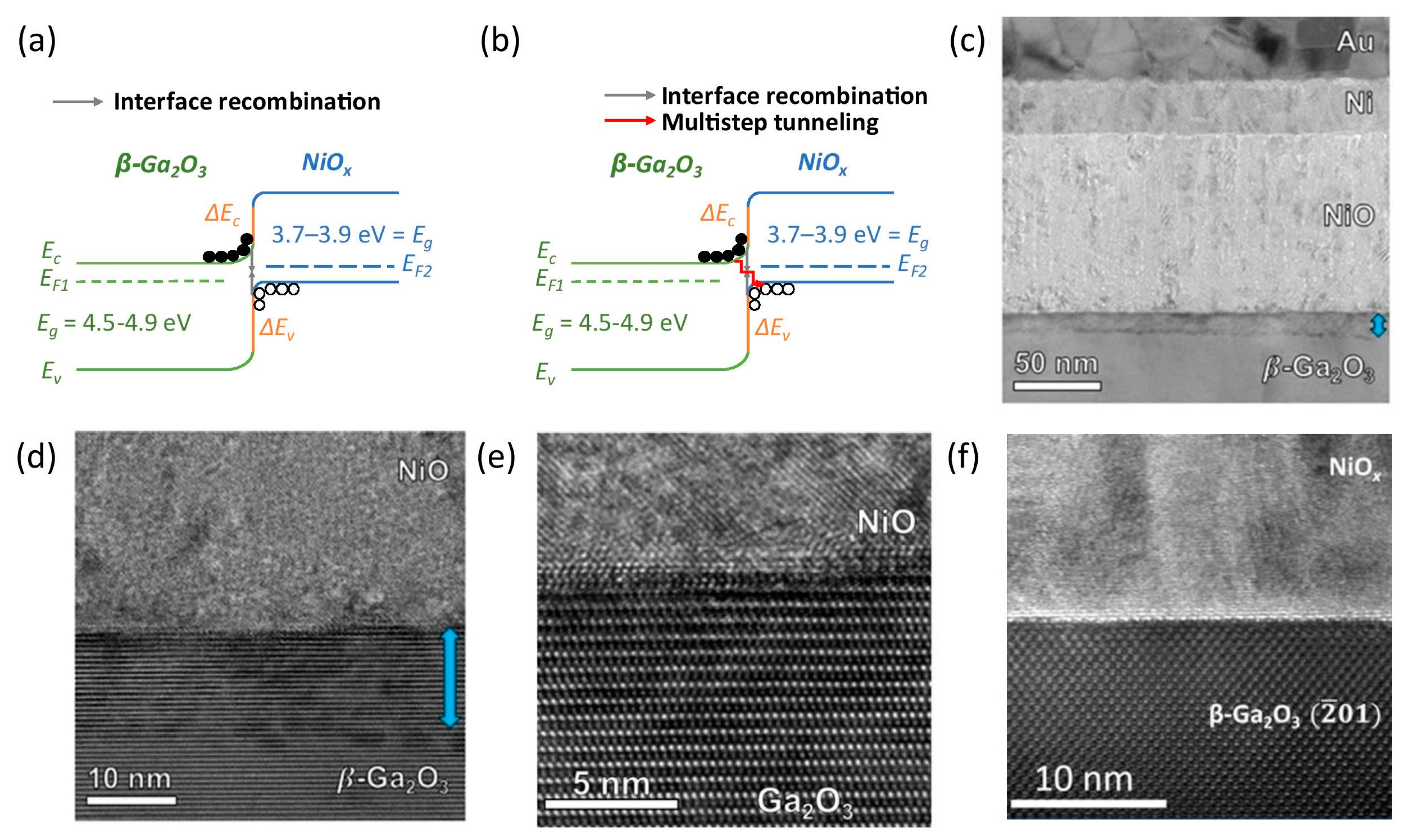
2. p-NiOx/β-Ga2O3 Heterojunction

Recently, NiOx has attracted significant attention as a promising p-type material for forming heterojunctions with n-type β-Ga2O3 [35]. While the incorporation of NiOx with β-Ga2O3 is a relatively recent development, NiOx has a well-established history of serving as hole contact in solar cell applications [38]. In particular, NiOx is highly regarded for its efficient extraction of generated holes, notably in perovskite solar cells [39]. Various NiOx deposition techniques are available, encompassing diverse methods such as sol-gel spin coating [40], RF sputtering [41], plasma-assisted laser deposition [42], electron beam (e-beam) evaporation [43], and the thermal oxidation of Ni [44]. Each of these methods presents its unique advantages and drawbacks. Among these techniques, RF sputtering is the most extensively researched method due to its capability to produce uniform polycrystalline films and control NiOx doping by adjusting the O2/Ar gas ratios and deposition pressure. More information about the RF sputtering deposition details can be found elsewhere [41,45,46]. It is important to note, however, that RF sputtering also causes damage to the β-Ga2O3 surface, as the high-energy plasma involved can induce interface states that can detrimentally impact the device performance [47]. Nevertheless, it has been demonstrated that sputtering can yield abrupt NiOx/β-Ga2O3 interfaces.
Li et al. [41] and Xia et al. [45] have conducted investigations into the band alignment, bandgap, and resistivity and the influence of the post-annealing temperature on NiOx films produced via RF magnetron sputtering. Their studies revealed that the bandgap of NiOx varied from 3.9 to 3.7 eV due to the annealing process, as illustrated in Figure 1a. In Figure 1b, the X-ray photoelectron spectroscopy (XPS) spectrum shows distinct Ni and O peaks. During the deposition process, Ni2+ and Ni3+ ions can interact with O2 to form NiO or Ni2O3, and the extent of this reaction strongly depends on the O2/Ar gas flow, as demonstrated in Figure 1d. Figure 1c,f illustrate that annealing led to a reduction in Ni2O3 and an increase in NiO, as further confirmed by X-ray diffraction (XRD) measurements. Additionally, it has been observed that the bandgap and resistivity of the films were closely associated with the O2/Ar gas flow (Figure 1e). Moreover, as described earlier, annealing resulted in a decrease in the bandgap and an increase in the resistivity of the films. Stoichiometric NiO is a wide-bandgap antiferromagnetic insulator [48]. The p-type properties of NiOx primarily arise from the presence of Ni vacancies and O interstitials (native accepter defects) [49]. NiOx can also be p-type-doped with alkali metals such as Li and K [50]. The elevated O2 flow during deposition and post-deposition annealing can enhance the stoichiometry of the NiOx films, resulting in films with a high resistivity and an improved hole mobility. In other words, native acceptor defects are thermally unstable and can be readily eliminated through an annealing process [49]. Furthermore, it has been observed that the polycrystalline nature improved with thermal annealing due to the crystalline grain growth [51].
Kokubun et al. [40] pioneered the development of the first NiOx/β-Ga2O3 heterostructure with Li-doped p-NiOx using a sol-gel spin coating process. While these devices exhibited favorable rectifying behavior, issues such as a high Ron and a low breakdown voltage (BV) limited their performance. It was deduced that the prevailing current transport mechanism was attributed to carrier recombination rather than carrier diffusion. Recent reports have further affirmed that, owing to the type-II band alignment of NiOx/β-Ga2O3 devices, carrier diffusion does not play a significant role under low-bias conditions. Instead, interface recombination (Figure 2a) and multi-step tunneling (Figure 2b) have emerged as the predominant mechanisms governing current transport in these heterojunctions [49,51,52]. Consequently, the quality of the interface holds the utmost importance for such devices. In Figure 2c, a transmission electron microscope (TEM) image of the fabricated NiOx/β-Ga2O3 diodes is presented, showing Au, Ni, NiOx, and β-Ga2O3 layers. It should be noted that Ni/Au contact acts as good Ohmic contact for NiOx with the aid of thermal annealing [51]. Figure 2d emphasizes the abrupt nature of the heterojunction using a high-resolution TEM (HRTEM) image; however, it also reveals regions that have incurred damage due to the high-energy plasma involved during sputtering (~150 W) [47]. To mitigate such issues, lower-energy plasma (~70 W) can be employed for NiOx deposition, resulting in an abrupt and smooth NiOx/β-Ga2O3 interface, as depicted in Figure 2e [53]. The damage that occurs during sputtering can introduce interface states that impact the device performance, potentially leading to increased leakage current and degradation of the device functionality. An alternative solution involves the use of e-beam-deposited NiOx, where the interface quality is improved, as illustrated in Figure 2f [43].
The anisotropic nature of NiOx/β-Ga2O3 in different crystal orientations has also been investigated. Deng et al. [54] investigated the dependence of the band alignment of NiOx/β-Ga2O3 heterostructures on various crystal orientations and revealed differences in the conduction and valence band offsets. Specifically, (–201) exhibited the lowest conduction and highest valence band offsets, while (010) showed the opposite trend. Subsequent investigations involved the use of e-beam-evaporated NiOx in various β-Ga2O3 crystal orientations, confirming clear interfaces across different orientations through HRTEM studies [43]. However, a significant disparity in the electronic properties was observed between (–201) [or (001)] and (010) orientations, manifesting as variations in the turn-on voltage, ON/OFF ratio, interface defect density, and temperature-dependent forward current transport. These differences are primarily attributed to distinct atomic configurations, the density of the dangling bonds, and variations in the interface trap-state densities across different crystal planes [43]. NiOx/β-Ga2O3 heterostructures commonly exhibit hysteresis, attributed to the interface traps at the NiOx/β-Ga2O3 heterojunction. Hao et al. [55] demonstrated a reduction in I–V hysteresis by subjecting the devices to 350 °C thermal annealing for 3 min post-fabrication. This annealing process resulted in a decrease in the interface trap states from 1.04 × 10¹² to 1.33 × 10¹¹ eV−1cm−2 and a reduction in the ideality factor from 3.02 to 1.27 after annealing. Following optimization, the devices achieved a BV of 1.63 kV with a high power figure of merit (PFOM) of 0.65 GW/cm2. Gong et al. [52] and Yan et al. [56] investigated interface trap states using capacitance–frequency (C–F) measurements and fitted the data with equations that assumed the distribution of the interface states into two energy states. The use of two states proved more effective, representing the interface states closer to the conduction band and others with deeper energy levels [43]. Gong et al. [52] and Yan et al. [56] both observed interface states in the order of ~1010 eV−1cm−2, which are among the lowest reported values. In addition, Li et al. [57] demonstrated the thermal annealing stability of NiOx/β-Ga2O3 p-n diodes from 300 to 500 °C in comparison with the as-deposited NiOx/β-Ga2O3 p-n diodes. Annealing at 300 °C resulted in a reduced low forward bias current, while the specific on-resistance (Ron,sp) remained relatively stable. However, annealing at higher temperatures from 400 to 500 °C degraded the Ron,sp due to the increased resistivity of the NiOx and degraded Ni/Au contact. Between 300 and 500 °C, the reverse leakage current decreased compared to in the as-deposited samples, with the 300 °C annealed sample exhibiting the highest BV. This indicates that temperature optimization is crucial to enhancing the heterointerface in these devices.
Lu et al. [58] demonstrated a NiOx/β-Ga2O3 heterojunction p-n diode with a low Ron,sp of 3.5 mΩ·cm2 and a high BV of 1.06 kV. A low reserve leakage of <1 µA/cm2 was observed until its breakdown. Zhang et al. [59] showcased a p-n diode featuring an impressive BV of 8.32 kV and an Ron,sp of 5.24 mΩ·cm2, resulting in a PFOM of 13.2 GW/cm2. In Figure 3a, the device configuration is depicted, featuring two NiOx regions and a field plate (FP) structure designed to withstand high BVs. Utilizing a double NiOx layer provided a low Ron,sp for the device while maintaining the BV [49]. The devices had drift regions of 7.5 and 13 µm with an unintentional doping (UID) concentration of 5–7 × 1015 cm−3. Figure 3b illustrates the forward I–V characteristics and Ron,sp curves for both device types. Additionally, these devices exhibited remarkable thermal stability up to 150 °C, as indicated in Figure 3c. Figure 3d presents the BV curves for these devices, marking a significant milestone in the NiOx/β-Ga2O3 p-n diode research. Li et al. [47] presented a noteworthy achievement with a 4.7 kV NiOx/β-Ga2O3 p-n diode through meticulous optimization of the thickness of the lower NiOx layer. Their device fabrication process aligned with the TCAD simulations, which indicated that extending the NiOx layer beyond the contact area could effectively alleviate electric field crowding, ultimately leading to a high BV. In Figure 3e, the device structure is depicted, while Figure 3f illustrates the forward I–V curves for the fabricated devices with varying thicknesses of the lower NiOx layer in comparison to a conventional β-Ga2O3 SBD. Figure 3g showcases the corresponding BVs, and Figure 3h presents the forward I–V curves in log scale, along with a comparison of the Ron,sp of the devices. These devices showed a notable PFOM of 2 GW/cm2. The same authors conducted a comprehensive study to optimize the NiOx doping, thickness, and junction termination extension (JTE) for NiOx/β-Ga2O3 devices with kV-class operation using Silvaco TCAD simulations [60]. Additionally, they successfully demonstrated high-BV devices with a maximum of 6.5 kV, achieved through thermal annealing optimization [57]. They also showcased p-n diodes with a 3.6 kV BV and a 4.8 A current capability within a 1 mm2 device area [61].
Xiao et al. [62] demonstrated a ~3.5 kV NiOx/β-Ga2O3 p-n diode with multiple JTEs of NiOx layers with different lengths (Figure 4a). This mechanism allows a gradual decrease in the effective charge carriers away from the device’s active region to smoothen the electric field crowding at the anode edge, as in Figure 4b. The bottom two JTEs consisted of lightly doped NiOx, while the top JTE was highly doped. This structure reduces the crowded electric field at the anode by reducing the surface electric field. Figure 4c shows the BV of devices with JTEs fabricated on two sets of wafers and without JTEs. Zhou et al. [63] presented a p-n diode featuring a bevel structure, as shown in Figure 4d, which exhibited remarkable characteristics, including a high BV of 2.04 kV and an impressive Ron,sp of 2.26 mΩ·cm2. These devices demonstrated a significant BFOM of 1.84 GW/cm2 (2.87 GW/cm2) with DC (pulsed) measurements. In Figure 4e, the BV curves of these diodes compared to a conventional β-Ga2O3 SBD with and without bevel edge termination are depicted. Figure 4f illustrates an effective reduction in electric field crowding using various bevel angles. Furthermore, this device exhibited a rapid reverse recovery time of 16.4 ns, outperforming Si fast-recovery diodes (Si FRDs), showing a significant advancement in current technology (Figure 4g). Hao et al. [64] demonstrated a 2.6 kV p-n diode by employing a JTE and annealing the device at 300 °C for 10 min. This diode exhibited stability at high temperatures and a BV of 1.77 kV at 250 °C. Furthermore, a low Ron,sp of 2.5 mΩ.cm2 resulted in a PFOM of 2.83 GW/cm2. Wang et al. [65] achieved a 2.41 kV p-n diode with a JTE and a small-angle beveled FP, boasting a remarkable Ron,sp of 1.12 mΩ·cm2 and a record BFOM of 5.18 GW/cm2. Gong et al. [66] demonstrated a 1.86 kV NiOx/β-Ga2O3 p-n diode that showed stability at 400 K with the use of double NiOx layers. Most recently, a NiOx/β-Ga2O3 p-n diode with a 7.5 kV BV, a PFOM of 6.2 GW/cm2, and an ON/OFF ratio of >1013 was demonstrated [67]. Collectively, these works highlight the immense potential of p-NiOx/β-Ga2O3 heterojunctions for advanced power device applications.
In addition to p-n junctions, NiOx can serve as a material for edge termination in β-Ga2O3 devices. This facilitates charge balance at the heterojunction, reducing electric field crowding and enhancing the device’s high-voltage-handling capabilities. NiOx-based JTEs [56,62,68], guard rings [69], and reduced surface field structures (RESURFs) [70,71] have been reported as edge terminations for β-Ga2O3 devices. Yan et al. [56] demonstrated a β-Ga2O3 SBD with NiOx heterojunction edge termination and a SiO2 FP structure (Figure 5a). These devices showed an average BV of 1.86 kV and an Ron,sp of 3.12 mΩ·cm2, yielding a BFOM of 1.11 GW/cm2. Furthermore, these devices showed a low interface trap density of 4.13 × 10¹⁰ eV−1cm−2. Figure 5b–d show the forward I–V, Ron,sp, and BV of SBDs with different anode diameters. Gong et al. [69] showcased a high-performance SBD with p-NiOx field-limiting rings (FLRs). A BFOM of 0.46 GW/cm2 was obtained with a 1.89 kV BV and an Ron,sp of 7.7 mΩ·cm2 for an SBD with an FLR width/spacing of 2 µm. It should be noted that an 8 µm JTE is also included in the design before the FLRs, as in Figure 5e. In this work, the authors fabricated p-n diodes, junction barrier Schottky diodes (JBS), conventional SBDs, and SBDs with 2 and 3 µm FLRs. Figure 5f–h show the forward I–V, Ron,sp, and BV of all the fabricated devices. Wang et al. [68] presented an SBD with three JTEs stacked on top of each other. These JTEs served to inhibit the electric field crowding in proximity to the Schottky contact, thus facilitating efficient charge extraction during device switching. Ma et al. [46] demonstrated the control of p-type doping in NiOx in the range of <1018 to 2 × 1018 cm−3 by changing the O2 partial pressure during RF magnetron sputtering. Precise control of p-type doping allows for charge balance in the n-type Ga2O3 region, leading to SBDs with ~8 kV BV. Recently, Qing et al. [71] presented an SBD featuring a NiOx RESURF structure that achieves a BV exceeding 10 kV, both at room temperature and 200 °C. Achieving a 10 kV performance at both room temperature and 200 °C marks a significant milestone in power electronics, highlighting the substantial potential of NiOx/β-Ga2O3 devices.
The JBS diodes combine the advantages of both SBDs and p-n diodes, offering the low turn-on voltage of SBDs and the low reverse leakage current of p-n diodes. During forward bias conditions, the Schottky regions are activated, allowing for efficient high-current transport, while at reverse bias, the Schottky regions were shielded from a high electric field due to the potential barrier from the p-n junction regions. Therefore, JBS devices have reduced resistive losses during forward bias (low turn-on) and the capability to handle high blocking voltages during reverse bias. The availability of p-type NiOx enables the fabrication of NiOx/β-Ga2O3 JBS diodes. Multiple JBS diodes have been successfully demonstrated to have the capability for high forward currents and high reverse blocking voltages, some reaching into the kV-class [72,73,74]. These achievements were made possible through the utilization of sputtered and thermally oxidized p-NiOx. Lv et al. [72] showed a JBS diode featuring an Ron,sp of 3.45 mΩ·cm2, along with a BV of 1.75 kV for a small-area device (100 µm2). This small-area device exhibited an impressive BFOM of 0.85 GW/cm2. For a larger-area device (1 mm2), it delivered 5 A of forward current and could withstand voltages up to ~0.7 kV. The NiOx was obtained through thermal oxidation, involving the exposure of a 5 nm Ni layer to a temperature of 600 °C for a duration of 10 min in an O2 atmosphere. In the resulting devices, SBD exhibited a turn-on voltage of 0.7 V, while the JBS diode had a slightly higher turn-on voltage of 1.0 V. This slight difference in voltage is due to the lateral depletion of the NiOx/β-Ga2O3 heterojunctions in the JBS diode. Yan et al. [73] reported a JBS diode with an Ron,sp of 1.94 mΩ·cm2 and a BV of 1.34 kV, resulting in a PFOM of 0.93 GW/cm2. The reduction in the β-Ga2O3 fin width was identified as a contributing factor to minimizing the reverse leakage current due to the enhanced sidewall depletion in the p-NiOx. The devices were manufactured using sputtered NiOx and varying β-Ga2O3 fin widths, specifically 1.5, 3, and 5 µm. Wu et al. [74] presented a JBS diode with and without a beveled FP. The incorporation of a beveled FP effectively reduced the electric field crowding from 7.8 to 5.1 MV/cm. These JBS diodes exhibited a di/dt of ~400 A/µs, a reverse recovery time of 26.8 ns, and a reverse recovery charge of 46.2 nC. Additionally, these devices were assembled and used to construct a voltage multiplier, demonstrating the practical applicability of NiOx/β-Ga2O3 JBS diodes. These results highlight the promising future of NiOx/β-Ga2O3 JBS diodes for high-current, high-voltage applications, paving the way for energy-efficient power electronics.
Over the years, β-Ga2O3-based lateral FETs have shown significant advancements in their electrical properties [7]. However, to approach the material’s limits with β-Ga2O3, achieving a lower Ron and a higher BV is imperative. Introducing NiOx beneath the gate in β-Ga2O3-based lateral FETs can enhance the Ron and improve the breakdown characteristics. This innovative configuration is referred to as a NiOx/β-Ga2O3-based junction field-effect transistor (JFET). In lateral FETs, higher channel doping can lead to a lower Ron, but it may also decrease the device’s BV. However, by incorporating NiOx under the gate, vertical depletion within β-Ga2O3 can allow for higher doping to optimize the Ron without compromising the device’s BV. Moreover, lateral depletion can reduce the electric field crowding on the drain side of the gate, further enhancing the device’s BV. Wang et al. [75] introduced the first NiOx/β-Ga2O3 JFET. The output and transfer characteristics of the devices feature an Ron of 38 mΩ·mm and an ON/OFF ratio of 1010. The device exhibited a subthreshold slope (SS) of 76 mV/Dec and a BV of 1.12 kV. Zhou et al. [76] presented a normally-off NiOx/β-Ga2O3 JFET with a recessed gate and a NiOx layer. This device exhibited a threshold voltage (Vth) of 0.9 V, an Ron of 151.5 Ω·mm, a BV of 0.98 kV, and a SS of 73 mV/Dec. These results indicate promising early developments for NiOx/β-Ga2O3 JFETs.
Recent advancements in NiOx/β-Ga2O3 heterojunction devices showcase their remarkable potential in high-voltage and high-power applications. These innovations encompass kV-class p-n diodes, NiOx edge-terminated Ga2O3 SBDs, JBS diodes, and JFETs. These devices offer enhanced electrical characteristics and exhibit impressive voltage handling capabilities ranging from ~1 to 10 kV. It is worth noting that even though p-type doping of β-Ga2O3 might be realized in the future, heterojunction p-n diodes still present some advantages over homojunction p-n diodes. Heterojunction diodes allow for tuning of the electronic properties based on the conduction and valence band offsets, which offers unique device characteristics, such as fast switching. Moreover, heterojunctions offer a cost-effective approach to device processing and enable advanced device designs that homojunction devices struggle to achieve. These remarkable advancements highlight the substantial progress made in the application of NiOx/β-Ga2O3 heterojunction devices, setting the stage for more energy-efficient and high-performance power electronics that are well suited to meet the demands of the next decade.

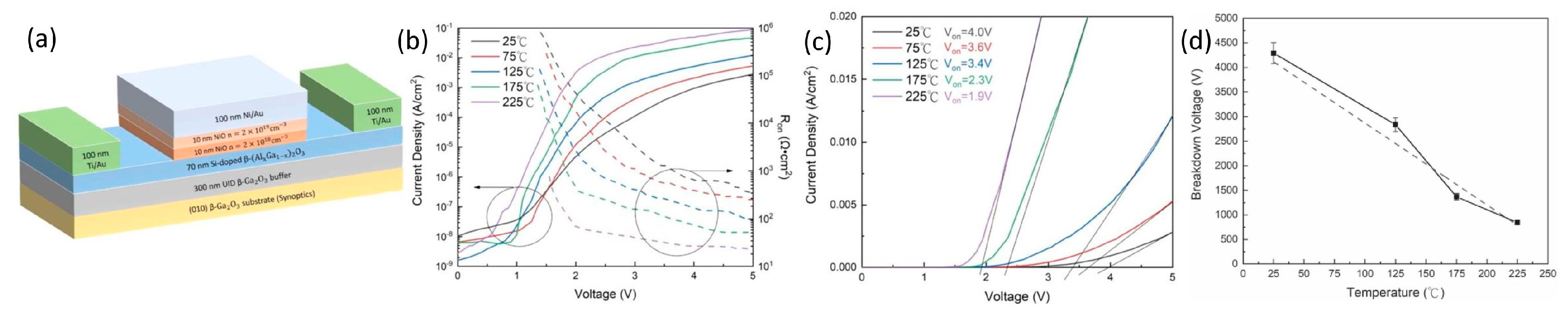
3. β-(AlxGa1−x)2O3/β-Ga2O3 Heterostructures

Alloying Ga2O3 with Al2O3 results in (AlxGa1−x)2O3 [77], which possesses an increased bandgap (e.g., 4.8–6.2 eV for x = 0 to 0.71) [78]. β-(AlxGa1–x)2O3 represents a monoclinic ternary alloy expected to offer a higher BFOM than β-Ga2O3, rendering it more suitable for power electronics applications [77]. A significant challenge lies in the production of high-quality β-(AlxGa1−x)2O3 layers with a substantial Al content, such as exceeding 20% in (010) β-Ga2O3 substrates [79]. This challenge arises from the fact that β-Ga2O3 has a monoclinic crystalline structure, while Al2O3 tends to adopt a corundum structure, leading to phase separation with a high Al content [80]. Additionally, the lattice mismatch with a high Al composition makes the epitaxial growth of β-(AlxGa1−x)2O3 on β-Ga2O3 a particularly demanding task. The primary approaches to growing β-(AlxGa1−x)2O3 are MBE [1] and MOCVD [78]. It is worth noting that other methods, such as pulsed laser deposition (PLD) [81] and sputtering [82], can also be employed for depositing β-(AlxGa1−x)2O3. This section primarily focuses on β-(AlxGa1−x)2O3/β-Ga2O3 heterostructures grown using MBE and MOCVD for power electronics.
Oshima et al. [83] presented the early stages of β-(AlxGa1−x)2O3/β-Ga2O3 growth using plasma-assisted MBE (PAMBE) on (100) β-Ga2O3 single crystals grown via the floating zone (FZ) method. During PAMBE growth, Ga and Al were evaporated from the effusion cells within RF-generated O plasma, resulting in the formation of β-(AlxGa1−x)2O3 thin films. More detailed growth parameters are provided elsewhere [76,77]. The Al content in the grown films was estimated by analyzing the shift in the high-resolution X-ray diffraction (HRXRD) spectra between the β-Ga2O3 and β-(AlxGa1−x)2O3 (020) peaks [84]. Using the equation x = 0.4727 × Δθ020, the Al composition in the (010) crystal orientations could be accurately determined, where Δθ020 represents the shift between the β-Ga2O3 and β-(AlxGa1−x)2O3 (020) peaks. They successfully incorporated Al up to x = 0.61 while maintaining the integrity of the β-phase crystal structure. However, at x = 0.68, the sample became polycrystalline, and the surface roughness of the samples was high. Stephen et al. [85] demonstrated the growth of β-(AlxGa1−x)2O3/β-Ga2O3 in (010) crystal orientations with a varying Al content in the range of x = 0.1 to 0.18 by optimizing the PAMBE growth conditions, such as substrate temperature and Al flux. These samples showed a good surface morphology with a maximum incorporation of 18% Al.
Zhang et al. [86] demonstrated a two-dimensional electron gas (2DEG) with high electron mobility through modulation doping and the use of Fe-doped semi-insulating β-Ga2O3 substrates. In the band diagram of β-(AlxGa1−x)2O3/β-Ga2O3, the Fermi level is above the conduction band (Figure 6c), leading to carrier accumulation at the interface. The β-(AlxGa1−x)2O3 layer can be modulation-doped with Si (δ-doping) (Figure 6a), and these free carriers migrate to the interface, resulting in the formation of a 2DEG with a sheet electron density of approximately 1012 cm−2. Figure 6b displays the HRXRD spectra of the grown β-(AlxGa1−x)2O3/β-Ga2O3 heterostructures. Two samples were grown with 130 and 360 nm buffer layers. The thicker buffer layer exhibited a higher 2DEG density due to the reduction in the backside depletion. Hall measurements were done using the van der Pauw geometry of the regrown highly doped β-Ga2O3 contact, and the charge density showed a weak temperature dependence (Figure 6d), indicating the presence of a formed 2DEG channel with a high low-temperature mobility of 2790 cm2/V·s at 50 K. The room temperature mobility was measured at 162 cm2/V·s for sample A and 180 cm2/V·s for sample B. The observed mobility was fitted using models for polar optical phonon scattering, remote impurity scattering, background impurity scattering, interface roughness scattering, and acoustic deformation potential scattering. A good agreement between the experimental values and fitting was observed, as demonstrated in Figure 6e,f. These findings demonstrate the formation of a 2DEG channel using β-(AlxGa1−x)2O3/β-Ga2O3 with Si modulation doping.
Miller et al. [87] reported the MOCVD growth of β-(AlxGa1−x)2O3/β-Ga2O3 using the metal–organic precursors trimethylaluminum (TMAl) and triethylaluminium (TEAl) as the Al source and triethylgallium (TEGa) as the Ga source and O2 for oxidation. They successfully achieved β-(AlxGa1−x)2O3 alloys with an Al content x up to 43% on sapphire substrates and demonstrated β-(AlxGa1−x)2O3/β-Ga2O3 superlattices. Compared to MBE, MOCVD is the industrial standard tool for the mass production of epitaxial compound semiconductor films. However, MBE operates under an ultra-high vacuum and requires the substrate temperature to be kept at <700 °C to reduce the decomposition of Ga2O3 into volatile suboxides. This limits the maximum Al2O3 incorporation into β-Ga2O3 to around 25% using MBE [88]. In contrast, the low to medium pressure in MOCVD allows the growth of β-(AlxGa1−x)2O3 at substrate temperatures >800 °C, with high solubility of the Al2O3 in β-Ga2O3. This prevents the formation of volatile suboxides and enables a high Al content in the β-(AlxGa1−x)2O3 barriers. The MOCVD growth has a large temperature window and precise control of the precursor flow, which makes it suitable for growing high-Al-fraction β-(AlxGa1−x)2O3 thin films. Such a high Al content is critical to realizing the formation of a 2DEG in the β-(AlxGa1−x)2O3/β-Ga2O3 heterojunctions and achieving a sufficiently large conduction band offset to confine the electrons [85]. Recent efforts involving the incorporation of Al through MOCVD have achieved 99% incorporation in the (100) orientation. However, the (010) and (−201) orientations exhibited lower Al incorporation, which was limited to 29% and 16%, respectively [89].
Ranga et al. [78] demonstrated n-type degenerate doping in β-(Al0.26Ga0.74)2O3 thin films grown through MOCVD and employed modulation doping in β-(Al0.26Ga0.74)2O3/β-Ga2O3 heterostructures. The Hall measurements unveiled a high carrier concentration ranging from 0.6 to 7.3 × 1019 cm−3, accompanied by a corresponding electron mobility of 53–27 cm2/V·s within the uniformly doped β-(Al0.26Ga0.74)2O3 layers. To assess the quality of the Si-doped β-(AlxGa1−x)2O3 epilayers, HRXRD measurements were taken to determine the Al composition of these epilayers. The results indicate Al mole fractions of approximately 0.26, closely matching the precursor molar flow ratio (25%) (Figure 7a), indicating that there were no pre-reactions with a complete incorporation of Al. Following the deposition of Ti/Au, Ohmic contact behavior was observed at room temperature. The temperature-dependent carrier concentration and mobility of the epilayers were assessed using Hall measurements (Figure 7b,c). Among the three samples grown using different silane (SiH4) flows, it was observed that sample A did not form Ohmic contact below 160 K. All three samples showed degenerate doping, as no carrier freeze-out was evident. To further confirm these observations, Figure 7d shows calculations of the separation from the Fermi level and conduction band considering different Al fraction values (α), where α = 0.22 (non-parabolic bands) and α = 0 (parabolic bands) for the three samples. This analysis confirmed that sample A exhibited weakly degenerate characteristics, while samples B and C were strongly degenerate. To achieve a total electron sheet charge of 2.3 × 1012 cm−2, modulation doping in a β-(Al0.26Ga0.74)2O3/β-Ga2O3 heterostructure was utilized, employing a uniformly doped β-(Al0.26Ga0.74)2O3 barrier layer alongside a thin spacer layer, as illustrated in the inset in Figure 7e. In Figure 7e, the HRXRD spectrum of the β-(Al0.26Ga0.74)2O3/β-Ga2O3 heterostructures on a Sn-doped substrate is presented. C–V measurements were conducted to measure the charge density and depth relationship. A peak corresponding to the 2DEG was observed near the estimated barrier thickness obtained from HRXRD, indicating modulation doping at this interface. The sudden drop in the C–V profile with depth (Figure 7f) confirms the carrier confinement at the heterointerface. Figure 7g presents the simulated band diagram using a Poisson–Schrödinger solver, which is closely aligned with the measured 2DEG value from the C–V profile.
Recently, Wang et al. [90] conducted an extensive study using TCAD simulations to gain insights into β-(AlxGa1−x)2O3/β-Ga2O3 heterostructures. The impact of the δ-doping concentration, the influence of the δ-doping position, and the effect of the δ-doping width were systematically investigated [90]. Multiple MODFETs have been developed after the successful growth of high-quality β-(AlxGa1−x)2O3/β-Ga2O3 heterostructures. Ahmadi et al. [91] reported β-(AlxGa1−x)2O3/β-Ga2O3 MODFETs grown via MBE with Ge as the n-type dopant. Their work resulted in a maximum current density of 20 mA/mm and a pinch-off voltage of −6 V, with a 2DEG sheet charge density of 1.2 × 1013 cm−2. Zhang et al. [86] employed the same structure grown using MBE to fabricate a β-(AlxGa1−x)2O3/β-Ga2O3 MODFET (Figure 6a). The heterostructure exhibited a high channel mobility at low temperatures, enabling the measurement of the Shubnikov–de Haas (SdH) oscillations in the transverse magnetoresistance under varying magnetic fields perpendicular to the sample surface. The calculated 2DEG densities from the SdH oscillations were 1.15 × 10¹² and 1.96 × 1012 cm−2 for samples A and B, respectively, aligning with low-field Hall measurements (Figure 6d). The transconductance (gm) decreased at a higher gate bias due to the reduced modulation efficiency resulting from the charge transfer into the barrier layer. The device exhibited ~109 rectification and an SS of ~91mV/Dec. The extracted Vth was 0.5 V, indicating a normally-off operation. High-frequency small-signal measurements conducted on this device showed a cutoff frequency of 3.1 GHz and a maximum oscillation frequency of 13.1 GHz at a VDS of 10 V and a VGS of 1.5 V. Kalarickal et al. [92] achieved a higher 2DEG sheet charge density, reaching up to 4.7 × 1012 cm−2, along with an effective mobility of 150 cm2/V·s using an ultra-thin spacer layer of just 1 nm. Increasing the 2DEG density is important as it aids in reducing the Ron and boosting the drain current in MODFETs. Moreover, a heightened charge density contributes to better screening of the strong polar optical phonon scattering, ultimately enhancing mobility. With a fixed conduction band offset, reducing the spacer thickness can be used to increase the 2DEG density. Furthermore, given that polar optical phonon scattering already limits mobility (~200 cm2/V·s), the potential impact of increased remote ionized impurity scattering on the total mobility is expected to be minimal with a 1 nm spacer. To prevent the diffusion of the Si δ-doping through the thin spacer, a lower growth temperature of 610 °C was used. Additionally, Kalarickal et al. [93] presented an effective field management approach to β-(AlxGa1−x)2O3/β-Ga2O3 MODFETs by employing an extremely high-k dielectric, BaTiO3 (k > 100). This innovative strategy facilitated a more uniform electric field distribution within the gate–drain region of the FET. Using this method, average breakdown fields of 1.5 and 4 MV/cm were achieved at gate-to-drain spacings (LGD) of 6 and 0.5 μm, respectively, with a high channel sheet charge density of 1.6 × 1013 cm−2. This resulted in a record PFOM of 376 MW/cm2 at an LGD of 3 μm.
Zhang et al. [94] demonstrated a double heterostructure MODFET (DHFET), as in Figure 8a. In this configuration, the β-(AlxGa1−x)2O3/β-Ga2O3/β-(AlxGa1−x)2O3 heterostructure acts as a quantum well and provides a 2DEG charge density higher than that of a single heterostructure. The Hall measurements indicated a mobility of 1775 cm2/V·s at 40 K and 123 cm2/V·s at room temperature. Figure 8b,c show the output and transfer curves of the demonstrated device with the physical dimensions and the biasing conditions. Figure 8d shows a simulation of the energy band diagram of the double heterostructure with and without parallel conducting channels. The important thing to note is that parallel conducting channels in the β-(AlxGa1−x)2O3 barrier layers can show up at high-impurity doping levels, as in the upper diagram of Figure 8d. These parasitic channels can lower mobility and affect the device performance. Therefore, precise control of Si doping is necessary to minimize the effect of parasitic conducting channels. The channel mobility at room temperature with the depth profile was extracted from a demonstrated transistor, as in Figure 8e. Later, Kalarickal et al. [95] reported a β-(Al0.18Ga0.82)2O3/Ga2O3 DHFET with an average field of 5.5 MV/cm, where a field management strategy with high-k BaTiO3 and low-k SiO2 and Al2O3 was also employed. The measured output characteristics of the β-(Al0.18Ga0.82)2O3/β-Ga2O3 DHFET showed an Ron of 28.6 Ω·mm. The corresponding transfer characteristics revealed a rectification ratio of ~107. The device breakdown voltage increased from 0.66 V to 1.11 kV as the LGD was increased from 1.15 to 5.15 μm. Vaidya et al. [96] reported high-performance β-(AlxGa1−x)2O3/β-Ga2O3 MODFETs with an elevated gm and a peak current density reaching 74 mA/mm. The small signal frequency measurements revealed impressive cutoff frequencies for the current gain and power gain, measuring 30 and 37 GHz, respectively, at a VGS of 1.2 V and a VDS of 10 V. Joishi et al. [97] demonstrated the breakdown characteristics of a field-plated β-(Al0.22Ga0.78)2O3/β-Ga2O3 MODFETs with Si3N4 passivation. A high BV of 1.37 kV was shown for a LGD = 16 µm device with an Ron,sp of 120 Ω·cm2. A comparably high average breakdown field of 3.9 MV/cm was obtained for an LGD = 320 nm device. This work shows effective passivation and field management strategies such as gate-connected FPs can significantly enhance the device performance. Recently, Wang et al. [98] explored a novel current aperture vertical transistor (CAVET) using TCAD simulation by incorporating a β-(AlxGa1−x)2O3/β-Ga2O3 heterostructure. These results indicate the potential of β-(AlxGa1−x)2O3/β-Ga2O3 MODFETs.
As the fabrication techniques for β-(AlxGa1−x)2O3/β-Ga2O3 heterostructures continue to advance, there is a promising future for employing these heterostructures in vertical devices. Nevertheless, the growth of the β-(AlxGa1−x)2O3 layer is constrained by the relatively slow growth rate, and as the layer thickness increases with a higher Al content, the film quality tends to deteriorate. Consequently, kV-class vertical devices based on β-(AlxGa1−x)2O3/β-Ga2O3 have not yet been realized. However, the use of UID of β-(AlxGa1−x)2O3 as a cap layer to enhance the BV of β-Ga2O3 SBDs has been explored [99]. Ahmadi et al. [100] investigated β-(AlxGa1−x)2O3/β-Ga2O3 heterostructures for the fabrication of SBDs with varying Al contents (Figure 9a). The diodes were produced by growing a 400 nm thick β-Ga2O3 layer on Sn-doped β-Ga2O3 (010) substrates, followed by a 100 nm thick β-(AlxGa1−x)2O3 layer with four different Al compositions. The HRXRD measurements (Figure 9b) confirmed the different Al compositions to be 0, 0.038, 0.084, and 0.164. The I–V characteristics revealed that similar Schottky barrier heights were observed in the SBDs with varying Al contents, which is attributed to the lateral fluctuations in the alloy composition leading to no variations in the barrier height. Figure 9c shows the temperature-dependent I–V data for an x = 0.084 composition. Furthermore, an increase in temperature resulted in a decrease in the ideality factor and an increase in the Schottky barrier height of the devices (Figure 9d), indicating an inhomogeneous Ni-Schottky contact. Sundaram et al. [99] introduced a novel structure to enhance the BV by growing a 30 nm β-(AlxGa1−x)2O3 capping layer to increase the Schottky barrier height, as shown in Figure 9e. They fabricated and compared β-(AlxGa1−x)2O3-capped (x = 0.22) SBDs with conventional β-Ga2O3 SBDs. Electrical measurements were conducted on both devices to determine the Schottky barrier height, and the resulting I–V curves are presented in Figure 9f. The extracted Schottky barrier heights for the β-Ga2O3-only and β-(AlxGa1−x)2O3-capped devices were 1.32 and 1.58 eV, respectively. This indicates an increase of 0.26 eV for the β-(AlxGa1−x)2O3-capped sample compared to the β-Ga2O3-only device. In Figure 9g, the reverse I–V characteristics of the two SBDs are shown, where the β-Ga2O3-only device and β-(AlxGa1−x)2O3-capped device exhibit BVs of 246 V and 387 V, respectively. Figure 9h depicts the simulated electric field around the Schottky contact’s edge at reverse breakdown. For the β-Ga2O3-only device, the maximum electric field under the anode edge was 2.5 MV/cm at breakdown (Figure 9h). In the β-(AlxGa1−x)2O3-capped device, the maximum field was 3.6 MV/cm. The additional Schottky barrier height created by the β-(AlxGa1−x)2O3 cap at the Schottky interface reduced the thermionic emission (TE) and thermionic field emission (TFE), thereby increasing the device’s BV.
To gain a deeper understanding of the leakage mechanisms of β-(AlxGa1−x)2O3 SBDs, Mudiyanselage et al. [101] conducted a study on the temperature-dependent reverse I–V characteristics of these devices. β-(AlxGa1−x)2O3 (x = 0.21) thin films were grown via MBE on a (010) Sn-doped β-Ga2O3 substrate, as depicted in Figure 9i. An anode made of Pt/Ti/Au was deposited to form the Schottky contact. Figure 9j presents the temperature-dependent forward I–V characteristics of the devices, showing an increasing current density with increasing temperature. Figure 9k displays the Schottky barrier heights and ideality factors of the vertical β-(AlxGa1−x)2O3 SBD calculated using the TE theory. As the temperature increased, the barrier height varied from 0.91 to 1.18 eV, while the ideality factor changed from 1.8 to 1.1. These changes are attributed to the non-uniform nature of the metal/semiconductor interface (i.e., inhomogeneous Schottky contact), resulting in the clear temperature-dependent behavior of both parameters. In Figure 9l, the leakage mechanisms for the SBDs are depicted. Different temperature ranges activate distinct processes within the semiconductor, as revealed by the reverse I–V measurements. Because of the high Schottky barrier height exceeding 1 eV in the vertical β-(AlxGa1−x)2O3 SBD, the most likely mechanisms include Poole–Frenkel emission (PFE), trap-assisted tunneling (TAT), Fowler–Nordheim tunneling (FNT), field emission (FE), and variable range hopping (VRH). To identify the dominant process, researchers often fit the reverse leakage data using the mathematical expressions of each model. Our analysis identified PFE and TAT as the two dominant mechanisms, with the other mechanisms playing a minor role.
Wan et al. [102] presented a lateral rectifier based on a NiOx/β-(Al0.21Ga0.79)2O3/β-Ga2O3 heterojunction. The structure of these rectifiers is depicted in Figure 10a, with the β-(AlxGa1−x)2O3/β-Ga2O3 heterostructure grown using a MOCVD system. NiOx was deposited using RF magnetron sputtering, and a bilayer structure was employed to optimize the sheet resistance and BV. Figure 10b shows the temperature-dependent forward I–V characteristics and the Ron,sp of the devices on a logarithmic scale, while Figure 10c shows the forward I-V characteristics on a linear scale with the extracted turn-on voltage at each temperature. The device current density increased with temperature, while the device turn-on voltage decreased as the temperature increased. Figure 10d shows the reverse I–V characteristics of the devices, where the negative temperature dependence of the BVs was observed, and thus the breakdown mechanism did not involve avalanche breakdown. They further studied devices with different diameters (50, 75, and 100 µm) [103]. The forward I–V curves of the devices with different diameters showed that the inclusion of the alloy did not significantly degrade the turn-on voltage. The highest BV value exceeding 7 kV was achieved in the 75 µm diameter lateral rectifier. A reverse I–V measurement at a low bias (<−100) indicated that the reverse leakage current in this bias range was primarily governed by TFE.
In short, the above research and the development of β-(AlxGa1−x)2O3/β-Ga2O3 heterostructures have shown considerable promise for power electronics. These heterostructures have been investigated in various device configurations, such as SBDs and MODFETs. The outcomes of these studies provide important insights into their electrical characteristics and potential applications. Further exploration and optimization of these heterostructures may lead to significant advancements in the field.

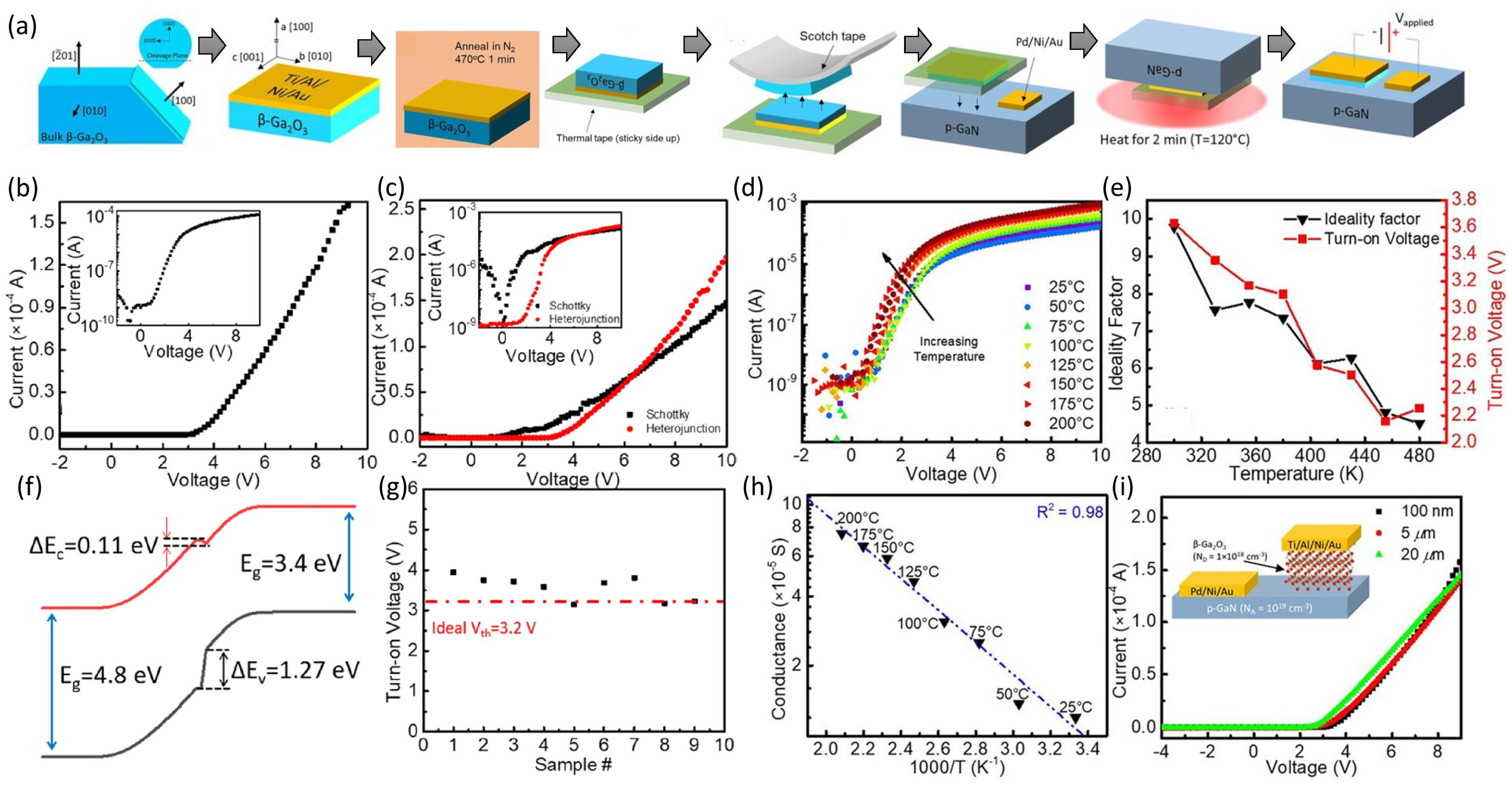
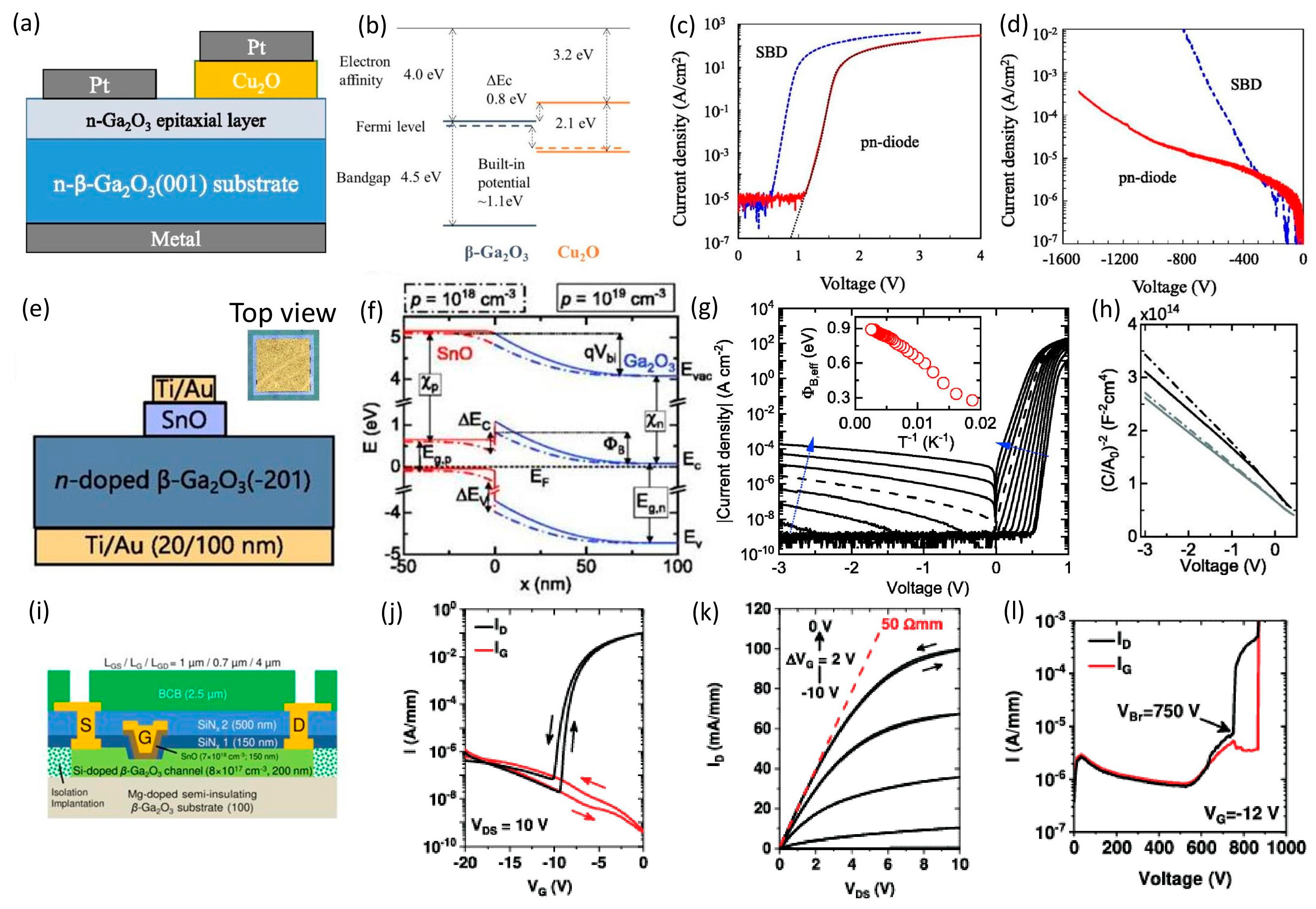
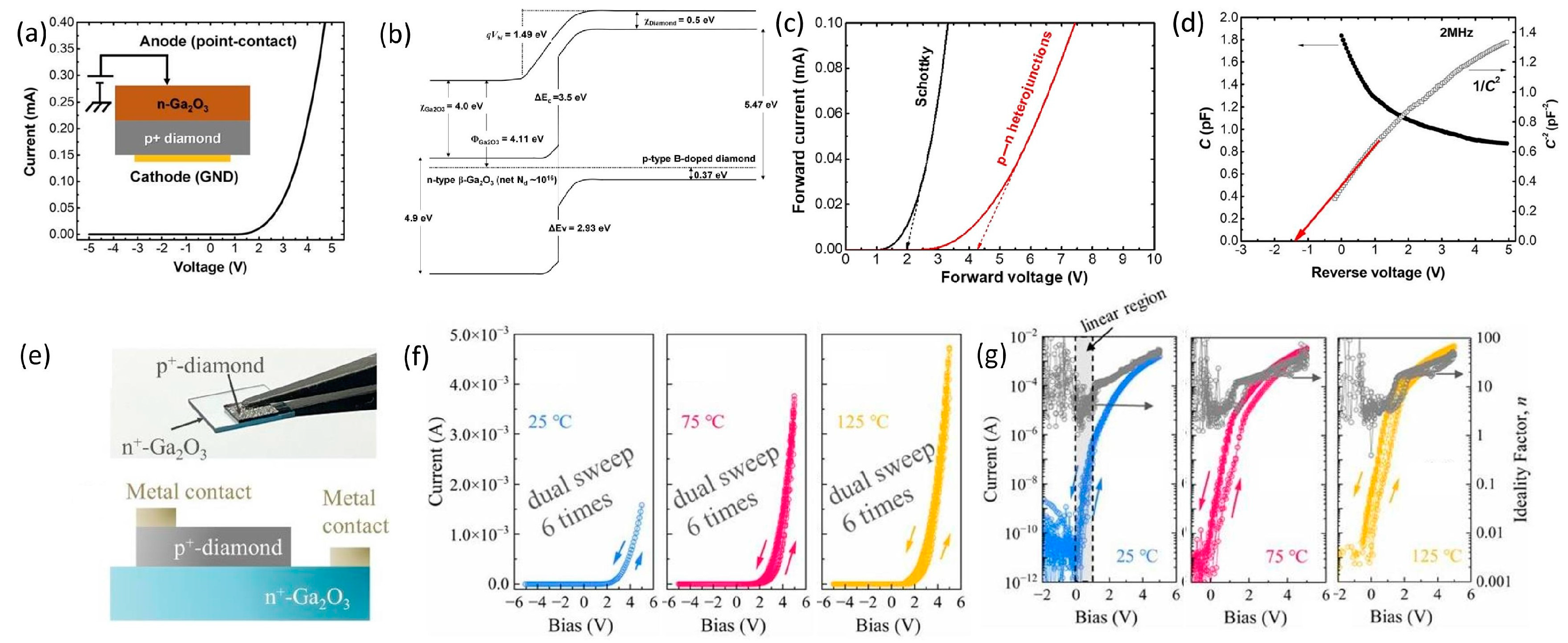
4. β-Ga2O3 Heterojunctions with Other p-Type Materials

In addition to NiOx, other p-type semiconducting materials with wide bandgaps, such as SiC and GaN, and metal oxides like Cu2O, CuI, and SnO have shown promise in forming p-n heterojunctions with β-Ga2O3. However, the exploration and utilization of these heterojunctions, in contrast to NiOx, are still in the early stages of development. Montes et al. [104] demonstrated a p-n heterojunction created using mechanically exfoliated β-Ga2O3 thermally bonded with p-GaN, as depicted in Figure 11a. The electrical characteristics of the devices are presented in Figure 11b on both the linear and logarithmic scales, while Figure 11c provides a comparison between the p-n diode and a simultaneously fabricated β-Ga2O3 SBD. These devices exhibited good temperature behavior, as shown in Figure 11d. Due to a significant number of interface states, the ideality factor for these devices was relatively large and decreased with an increasing temperature. The turn-on voltage of the devices was approximately 3.6 V at room temperature and decreased to around 2.2 V at 200 °C (Figure 11e). A band diagram of the devices was simulated using Silvaco TCAD in Figure 11f. The ideal turn-on voltage from the simulation was 3.2 V, while most of the fabricated devices exhibited a higher turn-on voltage, mainly due to the mechanical bonding of the p-n heterojunction (Figure 11g). In Figure 11h, an Arrhenius plot showed the conductance as a function of temperature at a forward bias of 3.5 V, demonstrating improved conductivity with increasing temperature. Moreover, p-GaN/β-Ga2O3 diodes were created with varying β-Ga2O3 thickness. Figure 11i shows the I–V characteristics of the p-n heterojunction with β-Ga2O3 thicknesses of 100 nm and 5 and 20 μm, indicating similar electrical characteristics across the different thicknesses. Mudiyanselage et al. [105] conducted theoretical investigations into edge termination structures for this p-n heterojunction, utilizing a 5 μm thick β-Ga2O3 drift layer, which has enabled the development of kV-class power diodes. Nandi et al. [106] have conducted research on JBS diodes utilizing this heterostructure, examined the switching characteristics of the devices, and obtained information on the reverse recovery behavior. Furthermore, Mudiyanselage et al. [107] studied JBS diodes by optimizing the p-GaN regions and varying their shapes to minimize the electric field crowding within the devices. Under forward bias, the Schottky regions became active, while under reverse bias, the p-n junctions effectively reduced the leakage currents. Deep UV photodiodes based on β-Ga2O3/SiC heterojunctions were demonstrated [108]. Nakagomi et al. [109] presented a β-Ga2O3/SiC heterojunction diode according to the thermal evaporation of Ga in O2 plasma onto a p-type 6H-SiC substrate. Song et al. [110] investigated a β-Ga2O3/4H–SiC MOSFET using fusion bonding.
Alternative materials such as Cu2O, CuI, and SnO have also been employed to create p-n heterojunctions with β-Ga2O3. Watahiki et al. [111] fabricated p-Cu2O/β-Ga2O3 diodes, as depicted in Figure 12a. The heterojunction demonstrated a significant forward current, pointing to a low conduction band offset at the p-Cu2O/β-Ga2O3 interface (Figure 12b). This device exhibited an Ron of 8.2 mΩ·cm2 and a BV of 1.49 kV (Figure 12c,d). An ideality factor of 1.31 suggested the diffusion current as the dominant mechanism. p-CuI/β-Ga2O3 was also demonstrated [112]. Furthermore, Budde et al. [113] reported vertical p-SnO/β-Ga2O3 heterojunction diodes via PAMBE (Figure 12e). The simulated band diagram is depicted in Figure 12f. These diodes exhibited excellent rectification with an ON/OFF ratio of 2 × 10⁸ at ±1 V, an ideality factor of 1.16, and an Ron,sp of 3.9 mΩ·cm2. The temperature-dependent I–V measurements indicated that TE dominated the transport in the forward bias (Figure 12g). The built-in voltage, calculated from the C–V measurements, was 0.96 V, as in Figure 12h. Moreover, Tetzner et al. [114] demonstrated an advanced lateral heterojunction FET (HJFET) utilizing p-type SnO in combination with (100)-oriented n-type β-Ga2O3 (Figure 12i). These transistors displayed stable switching properties with ON/OFF current ratios exceeding 106 and an Ron,sp below 50 Ω·mm, as demonstrated in Figure 12j,k. In the breakdown measurements, a heterojunction transistor with an LGD of 4 µm achieved a breakdown voltage of 0.75 kV (Figure 12l) and a calculated BFOM of 178 MW/cm2. In summary, p-SnO/β-Ga2O3 and p-Cu2O/β-Ga2O3 diode structures exhibit relatively lower ideality factors, indicating their potential for high-frequency applications and offer promising performance in terms of Ron, BV, and BFOM. However, the calculated critical breakdown field still falls short of the theoretical value for β-Ga2O3, possibly due to surface defects during film growth and the absence of electric field management design. Future studies should systematically explore these characteristics as well.
These findings highlight the potential to enhance novel materials when combined with β-Ga2O3. A key challenge in developing these devices is effectively managing the interface states. The presence of interface states, resulting from factors like the growth or deposition method and lattice mismatch, can limit the device performance. The introduction of a transition layer, such as h-BN, between these materials could help reduce interface states and lead to an improved device performance.

5. β-Ga2O3 Heterostructures with Other UWBG Semiconductors

Researchers are also investigating the use of other UWBG materials such as diamond, AlN, and BN to form heterostructures with β-Ga2O3. Diamond is a promising material for next-generation power electronic devices due to its high carrier mobilities (4500 cm2/V·s for electrons and 3800 cm2/V·s for holes), higher critical electric field (>10 MV/cm), higher thermal conductivity (2000 W/m·K), and ultra-wide bandgap (5.5 eV) [115,116]. It also has p-type doping with boron (B) and has an acceptor concentration ranging from 1015 to 1021 cm−3, which make it an attractive candidate material for exploiting the full potential of β-Ga2O3 [117]. Matsumae et al. [118] have demonstrated the direct bonding of β-Ga2O3 and diamond substrates. OH-terminated β-Ga2O3 and diamond surfaces were directly bonded using a thermal dehydration reaction at low temperatures (250 °C). Recently, MOCVD growth of β-Ga2O3 on (001) diamond substrates was demonstrated [119]. Furthermore, heteroepitaxial growth of β-Ga2O3 thin films on single crystalline diamond (111) wafers using RF magnetron sputtering was also demonstrated [120]. Mishra et al. [121] conducted a theoretical investigation into the electrical and thermal characteristics of diamond/β-Ga2O3 super-junction Schottky barrier diodes (SJSBDs) with a 20 nm thick Al2O3 interlayer. This interlayer will play a crucial role in practical device realization because it protects the Ga2O3 from microwave plasma etching during the chemical vapor deposition (CVD) growth of diamond. Furthermore, the oxide interlayer aids in securing the nano-diamond seeds necessary for the growth of polycrystalline diamond (PCD). Additionally, this design permits the attainment of high electric fields in both the p-type and n-type regions, exploiting the UWBG characteristics of these materials. Achieving a charge balance between the p and n regions is essential for the device to operate effectively at the highest BV. A charge imbalance would diminish the device performance by inducing an asymmetric electric field within the device, leading to premature breakdown. Notably, the incorporation of a p-type diamond into this structure also enhanced the device’s thermal performance, addressing one of the main challenges associated with β-Ga2O3, i.e., low-thermal conductivity [3], as pointed out earlier. Sittimart et al. [117] employed a low-temperature direct bonding method to fabricate diamond/β-Ga2O3 p-n heterojunction diodes (inset Figure 13a). These diodes exhibited an impressive rectifying ratio exceeding 108 at ± 10 V. Additionally, the leakage current was exceptionally low, measuring less than 10−12 A. The forward I–V curve is presented in Figure 13a. The ideality factor and barrier height for these diodes were estimated to be 2.7 and 1.5 eV, respectively. The band alignment of this heterojunction is illustrated in Figure 13b. In Figure 13c, a comparison is presented between the β-Ga2O3 SBD and the diamond/β-Ga2O3 p-n heterojunction, highlighting their differences and characteristics. Figure 13d shows the C–V characteristics of one of the demonstrated p-n diodes. Malakoutian et al. [122] demonstrated polycrystalline diamond epitaxial growth on β-Ga2O3 with a CVD method for device-level thermal management. A thermal conductivity of 110 W/m·K for the diamond and a thermal boundary resistance of 30.2 m2K/GW were measured. Recently, Rahaman et al. [123] demonstrated the mechanical integration of diamond/β-Ga2O3 as an effortless fabrication method to demonstrate a p-n heterojunction, as in Figure 13e. The devices show a remarkable ON/OFF ratio of 108 and a low ideality factor of 1.28, while the device operation spans from 25 °C up to 125 °C (Figure 13f,g). This work provides a novel pathway for integrating UWBG material with different thermal expansion coefficients.
AlN exhibits a wide bandgap of 6.2 eV, making it highly suitable for power applications [124]. Chen et al. [125] conducted a study on the band alignment of AlN/β-Ga2O3 heterostructures and determined valence band offsets of 0.09 eV (type II alignment) for AlN grown via plasma-enhanced atomic layer deposition (PEALD) on β-Ga2O3 and 0.72 eV (type I alignment) for AlN prepared using thermal atomic layer deposition (T-ALD) on β-Ga2O3. Song et al. [126] explored an AlN/β-Ga2O3 heterostructure, employing polarization-induced doping to create high-performance enhancement-mode transistors with a 2DEG concentration reaching up to 8.1 × 1019 cm−3 (Figure 14a). A p-GaN gate was utilized to achieve a normally-off operation with a positive Vth. In Figure 14b, the distribution of the polarization charge in the different material regions is depicted, and Figure 14c shows the band diagram and 2DEG confinement, with Figure 14d displaying the device’s output characteristics. Nonetheless, growing high-quality AlN or Al-rich AlGaN thin films on β-Ga2O3 with good interfaces remains a challenge. Furthermore, since GaN has a narrower bandgap compared to β-Ga2O3, p-GaN itself has a lower critical field, which could potentially impact the device breakdown performance. Alternatively, using wider-bandgap p-type materials like p-AlGaN layers may offer advantages for gate materials. Furthermore, researchers are actively exploring the use of UWBG materials such as AlN and h-BN thin interlayers for β-Ga2O3 SBDs to achieve higher Schottky barrier heights and BVs. Recently, Baskaran et al. [127] investigated an AlN/β-Ga2O3 high-electron-mobility transistor (HEMT) on a SiC substrate for power converters and RF applications. Similar to AlN, BN is emerging as a UWBG material with a bandgap of ~6.0 eV and a critical field of ~10 MV/cm [128,129,130]. However, BN predominantly functions as a dielectric material rather than a semiconductor. A recent study by Xu et al. [130] showcased a kV-class β-Ga2O3 metal–insulator–semiconductor (MIS) diode incorporating a thin BN nitride layer aimed at enhancing device breakdown. The introduction of a 2.8 nm thin BN layer (Figure 14e) significantly elevated the device breakdown from 0.73 to 1.03 kV, highlighting the potential of this approach (Figure 14h). It is worth noting that this enhancement may result in an increased turn-on voltage and Ron,sp in the devices. Nevertheless, this technique serves as an effective means of tuning the device breakdown voltage. Figure 14f,g depict the forward I–V curves of both diodes, with and without the BN interlayer, on the linear and log scales. These results indicate that the combination of UWBG materials with Ga2O3 opens up new device architectures to explore.

6. β-Ga2O3 Heterostructures with 2D Materials

Recent years have witnessed significant advancements in 2D materials such as MoS2, WS2, WSe2, BP, and graphene [131,132]. Researchers have also explored the integration of 2D materials with β-Ga2O3. This section discusses some of the noteworthy research efforts and the latest developments. Yan et al. [133] demonstrated graphene/β-Ga2O3 vertical barristor heterostructures, and the device structure is depicted in Figure 15a. The fabrication process began with the mechanical exfoliation and transfer of graphene onto a SiO2/Si wafer, with the SiO2 layer measuring 285 nm in thickness. Next, β-Ga2O3 was exfoliated and transferred onto the wafer, where it overlapped with the graphene flake. β-Ga2O3 was intentionally kept undoped to provide a reasonable estimate of the breakdown field. After that, the contact regions were defined using e-beam lithography, followed by Ti/Au (5/45 nm) metal evaporation. Figure 15b presents a cross-sectional energy band diagram of the heterostructure, illustrating the charge transport mechanisms under different biasing conditions. The graphene layer plays a crucial role in enabling electron injection while enabling a high electric field due to the back-gate (Si substrate) bias. Cross-sectional HRTEM images of the fabricated graphene/β-Ga2O3 heterostructure are showcased in Figure 15c. Electrical measurements revealed a remarkable breakdown field of 5.2 MV/cm perpendicular to the (100) plane.
Kim et al. [134] demonstrated a depletion-mode β-Ga2O3 HJFET with an n-channel configuration, achieved via van der Waals bonding to an exfoliated p-WSe2 flake, as shown in Figure 15d. The use of van der Waals interaction allows for layered materials separated from their bulk crystals to be assembled into a strain-free heterostructure. Figure 15e shows a band diagram of the device with its conduction and valence band offsets. The p-WSe2/β-Ga2O3 heterostructure diode exhibited typical diode characteristics with a rectifying ratio of ~105. The layered HJFETs displayed exceptional output (Figure 15f) and transfer characteristics. These devices boasted a high ON/OFF ratio of ~108 and a low SS of ~133 mV/Dec. Saturated output currents were observed with a Vth of −5.1 V, and a three-terminal breakdown voltage of 144 V was obtained. Leblanc et al. [135] demonstrated p-n heterojunctions using p-WSe2, WS2, and BP on β-Ga2O3, and the fabricated device structure is depicted in Figure 15g. Their study focused on optimizing 2D/3D vertical diodes on β-Ga2O3 by considering three key factors, including the β-Ga2O3 crystal orientation, the choice of 2D material, and the type of metal contact. The I–V characteristics of the p-n diodes in (–201) β-Ga2O3 orientations are presented in Figure 15h. Figure 15i shows the variation in the ideality factor with the choice of 2D material and β-Ga2O3 crystal orientations. These results suggest that 2D/3D β-Ga2O3 vertical heterojunctions can be optimized by employing substrate orientation (–201), combining it with 2D WS2 exfoliated layers and Ti contact. These optimized devices exhibited record rectification ratios (>106) while maintaining a high ON-current density (>103 Acm−2), making them promising for applications in power rectifiers. The above results showcase the potential of 2D material/β-Ga2O3 for transistors and diodes.

7. Conclusions and Outlook

β-Ga2O3 heterostructures and heterojunctions hold significant promise for future power electronics technology advancements. A wide range of heterojunctions/heterostructures and configurations have been explored to harness the unique properties of β-Ga2O3 for high-power electronics. NiOx/β-Ga2O3 heterojunctions open the door for advanced power devices, high-frequency applications, and enhanced functionality. Further optimizations and innovations in incorporating NiOx/β-Ga2O3 heterostructures into power devices can be expected, and the stability and reliability of such devices warrant special attention. Precise control over the p-type doping of NiOx is essential to achieve the necessary charge balance between the p- and n-type regions, as any imbalance can hinder the device BV and overall performance. While researchers have demonstrated some degree of tunability in p-type doping, further optimization of NiOx/β-Ga2O3 heterojunction diodes is warranted. Exploring various edge termination structures and multidimensional device architectures is crucial to surpass unipolar BFOM limitations. Novel device architectures hold promise for achieving higher performance levels. β-(AlxGa1−x)2O3/β-Ga2O3 heterostructures have unique properties, such as high breakdown voltages and excellent 2DEG control, making them the workhorse for high-frequency devices. In these heterostructures, precise control over the Si δ-doping channel width and position is paramount. At elevated doping levels, parasitic conduction channels may arise, emphasizing the importance of accurate Si doping for an optimal device performance. Implementing multiple-channel devices with multiple quantum wells could enhance the device performance compared to single- or double-channel devices. The inclusion of UWBG materials like diamond, AlN, and BN brings new opportunities for β-Ga2O3 electronics as both device active regions and passivation structures. The growth of wide- and ultra-wide-bandgap materials on Ga2O3 necessitates reducing the defect density and improving the material quality due to significant lattice mismatches. Interface engineering and optimized growth techniques hold the potential to enhance the material quality and consequently the device performance. Furthermore, the versatile nature of β-Ga2O3 allows it to be combined with different materials, including 2D materials like graphene, MoS2, WS2, WSe2, and BP for novel device applications, and new and exciting material combinations are expected. Incorporating 2D materials presents challenges, as the surface roughness plays a crucial role in promoting the adhesion between Ga2O3 and 2D materials. Future developments may involve exploring new material combinations and device configurations that leverage the anisotropic nature of β-Ga2O3. Additionally, improving the Ohmic and Schottky contacts in 2D/3D β-Ga2O3 devices is essential to enhancing their current transport capabilities. While there are challenges, such as interface engineering and material compatibility, active research is ongoing to address these issues. Furthermore, issues arising from the low thermal conductivity of Ga2O3 can be mitigated with the use of heterostructures involving integration with high-thermal-conductivity diamond and SiC. The research on β-Ga2O3 heterostructures and heterojunctions has the potential to significantly expand the capability of Ga2O3 power electronics and facilitate their maturity. This review can be a valuable reference for recent developments in Ga2O3-based heterojunctions and serve as an important gateway to further development of Ga2O3-based electronics and their heterostructures to address future energy demands.

Author Contributions

Conceptualization, D.H.M. and H.F.; writing—original draft preparation, D.H.M., B.D., J.A., D.W., Z.H. and H.F.; writing—review and editing, D.H.M., B.D., K.F., Y.Z. and H.F.; supervision, K.F., Y.Z. and H.F.; funding acquisition, H.F. All authors have read and agreed to the published version of the manuscript.

Funding

This work was supported as part of ULTRA, an Energy Frontier Research Center funded by the U.S. Department of Energy (DOE), the Office of Science, Basic Energy Sciences (BES), under Award # DE-SC0021230. This work is also partially supported by the National Science Foundation (NSF) under Award # 2302696.

Data Availability Statement

The data supporting the results and conclusions of this study are available within the article.

Conflicts of Interest

The authors declare no conflicts of interest.

References

  1. Gallium Oxide; Springer: Berlin/Heidelberg, Germany, 2020; Volume 293. [CrossRef]
  2. Higashiwaki, M.; Sasaki, K.; Kuramata, A.; Masui, T.; Yamakoshi, S. Gallium Oxide (Ga2O3) Metal-Semiconductor Field-Effect Transistors on Single-Crystal β-Ga2O3 (010) Substrates. Appl. Phys. Lett. 2012, 100, 013504. [Google Scholar] [CrossRef]
  3. Higashiwaki, M. β-Ga2O3 Material Properties, Growth Technologies, and Devices: A Review. AAPPS Bull. 2022, 32, 3. [Google Scholar] [CrossRef]
  4. Tolbert, L.M. Power Electronics for Distributed Energy Systems and Transmission and Distribution Applications: Assessing the Technical Needs for Utility Applications; Oak Ridge National Laboratory: Oak Ridge, TN, USA, 2005. [Google Scholar]
  5. Wang, C.; Zhang, J.; Xu, S.; Zhang, C.; Feng, Q.; Zhang, Y.; Ning, J.; Zhao, S.; Zhou, H.; Hao, Y. Progress in state-of-the-art technologies of Ga2O3 devices. J. Phys. D Appl. Phys. 2021, 54, 243001. [Google Scholar] [CrossRef]
  6. Green, A.J.; Speck, J.; Xing, G.; Moens, P.; Allerstam, F.; Gumaelius, K.; Neyer, T.; Arias-Purdue, A.; Mehrotra, V.; Kuramata, A.; et al. β-Gallium Oxide Power Electronics. APL Mater. 2022, 10, 029201. [Google Scholar] [CrossRef]
  7. Chabak, K.D.; Leedy, K.D.; Green, A.J.; Mou, S.; Neal, A.T.; Asel, T.; Heller, E.R.; Hendricks, N.S.; Liddy, K.; Crespo, A.; et al. Lateral β-Ga2O3 Field Effect Transistors. Semicond. Sci. Technol. 2020, 35, 013002. [Google Scholar] [CrossRef]
  8. Pearton, S.J.; Yang, J.; Cary, P.H., IV; Ren, F.; Kim, J.; Tadjer, M.J.; Mastro, M.A. A Review of Ga2O3 Materials, Processing, and Devices. Appl. Phys. Rev. 2018, 5, 011301. [Google Scholar] [CrossRef]
  9. Mastro, M.A.; Eddy, C.R., Jr.; Tadjer, M.J.; Hite, J.K.; Kim, J.; Pearton, S.J. Assessment of the (010) β-Ga2O3 Surface and Substrate Specification. J. Vac. Sci. Technol. A 2020, 39, 013408. [Google Scholar] [CrossRef]
  10. Goto, K.; Konishi, K.; Murakami, H.; Kumagai, Y.; Monemar, B.; Higashiwaki, M.; Kuramata, A.; Yamakoshi, S. Halide Vapor Phase Epitaxy of Si Doped β-Ga2O3 and Its Electrical Properties. Thin Solid Films 2018, 666, 182–184. [Google Scholar] [CrossRef]
  11. Higashiwaki, M. MBE Growth and Device Applications of Ga2O3. In Molecular Beam Epitaxy; John Wiley & Sons, Inc.: Hoboken, NJ, USA, 2019; pp. 411–422. ISBN 9781119354987. [Google Scholar]
  12. Seryogin, G.; Alema, F.; Valente, N.; Fu, H.; Steinbrunner, E.; Neal, A.T.; Mou, S.; Fine, A.; Osinsky, A. MOCVD Growth of High Purity Ga2O3 Epitaxial Films Using Trimethylgallium Precursor. Appl. Phys. Lett. 2020, 117, 262101. [Google Scholar] [CrossRef]
  13. Sinha, G.; Adhikary, K.; Chaudhuri, S. Effect of Annealing Temperature on Structural Transformation of Gallium Based Nanocrystalline Oxide Thin Films and Their Optical Properties. Opt. Mater. 2007, 29, 718–722. [Google Scholar] [CrossRef]
  14. Suman, S.; Mukurala, N.; Kushwaha, A.K. Annealing Induced Surface Restructuring in Hydrothermally Synthesized Gallium Oxide Nano-Cuboids. J. Cryst. Growth 2021, 554, 125946. [Google Scholar] [CrossRef]
  15. Fujihara, S.; Shibata, Y.; Hosono, E. Chemical Deposition of Rodlike GaOOH and β-Ga2O3 Films Using Simple Aqueous Solutions. J. Electrochem. Soc. 2005, 152, C764. [Google Scholar] [CrossRef]
  16. Ghazali, N.M.; Mahmood, M.R.; Yasui, K.; Hashim, A.M. Electrochemically Deposited Gallium Oxide Nanostructures on Silicon Substrates. Nanoscale Res. Lett. 2014, 9, 120. [Google Scholar] [CrossRef]
  17. Chiang, J.-L.; Yadlapalli, B.K.; Chen, M.-I.; Wuu, D.-S. A Review on Gallium Oxide Materials from Solution Processes. Nanomaterials 2022, 12, 3601. [Google Scholar] [CrossRef]
  18. Al-Hardan, N.H.; Abdul Hamid, M.A.; Jalar, A.; Firdaus-Raih, M. Unleashing the Potential of Gallium Oxide: A Paradigm Shift in Optoelectronic Applications for Image Sensing and Neuromorphic Computing Applications. Mater. Today Phys. 2023, 38, 101279. [Google Scholar] [CrossRef]
  19. Asif, M.; Kumar, A. Resistive Switching in Emerging Materials and Their Characteristics for Neuromorphic Computing. Mater. Today Electron 2022, 1, 100004. [Google Scholar] [CrossRef]
  20. Neal, A.T.; Mou, S.; Rafique, S.; Zhao, H.; Ahmadi, E.; Speck, J.S.; Stevens, K.T.; Blevins, J.D.; Thomson, D.B.; Moser, N.; et al. Donors and Deep Acceptors in β-Ga2O3. Appl. Phys. Lett. 2018, 113, 062101. [Google Scholar] [CrossRef]
  21. Ma, N.; Tanen, N.; Verma, A.; Guo, Z.; Luo, T.; Xing, H.; Jena, D. Intrinsic Electron Mobility Limits in β-Ga2O3. Appl. Phys. Lett. 2016, 109, 212101. [Google Scholar] [CrossRef]
  22. Kang, Y.; Krishnaswamy, K.; Peelaers, H.; Van de Walle, C.G. Fundamental Limits on the Electron Mobility of β-Ga2O3. J. Phys. Condens. Matter 2017, 29, 234001. [Google Scholar] [CrossRef]
  23. Ghosh, K.; Singisetti, U. Ab Initio Calculation of Electron–Phonon Coupling in Monoclinic β-Ga2O3 Crystal. Appl. Phys. Lett. 2016, 109, 072102. [Google Scholar] [CrossRef]
  24. Ghosh, K.; Singisetti, U. Ab Initio Velocity-Field Curves in Monoclinic β-Ga2O3. J. Appl. Phys. 2017, 122, 035702. [Google Scholar] [CrossRef]
  25. Guo, Z.; Verma, A.; Wu, X.; Sun, F.; Hickman, A.; Masui, T.; Kuramata, A.; Higashiwaki, M.; Jena, D.; Luo, T. Anisotropic Thermal Conductivity in Single Crystal β-Gallium Oxide. Appl. Phys. Lett. 2015, 106, 111909. [Google Scholar] [CrossRef]
  26. Gopalan, P.; Knight, S.; Chanana, A.; Stokey, M.; Ranga, P.; Scarpulla, M.A.; Krishnamoorthy, S.; Darakchieva, V.; Galazka, Z.; Irmscher, K.; et al. The Anisotropic Quasi-Static Permittivity of Single-Crystal β-Ga2O3 Measured by Terahertz Spectroscopy. Appl. Phys. Lett. 2020, 117, 252103. [Google Scholar] [CrossRef]
  27. Fu, H.; Chen, H.; Huang, X.; Baranowski, I.; Montes, J.; Yang, T.-H.; Zhao, Y. A Comparative Study on the Electrical Properties of Vertical ( 2 - 01) and (010) β-Ga2O3 Schottky Barrier Diodes on EFG Single-Crystal Substrates. IEEE Trans. Electron Devices 2018, 65, 3507–3513. [Google Scholar] [CrossRef]
  28. Lyons, J.L. A Survey of Acceptor Dopants for β-Ga2O3. Semicond. Sci. Technol. 2018, 33, 05LT02. [Google Scholar] [CrossRef]
  29. He, H.; Orlando, R.; Blanco, M.A.; Pandey, R.; Amzallag, E.; Baraille, I.; Rérat, M. First-Principles Study of the Structural, Electronic, and Optical Properties of Ga2O3 in Its Monoclinic and Hexagonal Phases. Phys. Rev. B 2006, 74, 195123. [Google Scholar] [CrossRef]
  30. Gake, T.; Kumagai, Y.; Oba, F. First-Principles Study of Self-Trapped Holes and Acceptor Impurities in Ga2O3 Polymorphs. Phys. Rev. Mater. 2019, 3, 44603. [Google Scholar] [CrossRef]
  31. Ji, X.; Lu, C.; Yan, Z.; Shan, L.; Yan, X.; Wang, J.; Yue, J.; Qi, X.; Liu, Z.; Tang, W.; et al. A Review of Gallium Oxide-Based Power Schottky Barrier Diodes. J. Phys. D Appl. Phys. 2022, 55, 443002. [Google Scholar] [CrossRef]
  32. Higashiwaki, M.; Wong, M.H.; Goto, K.; Murakami, H.; Kumagai, Y. (Keynote) Nitrogen-Ion Implantation Doping of Ga2O3 and Its Application to Transistors. ECS Meet. Abstr. 2019, MA2019-02, 1169. [Google Scholar] [CrossRef]
  33. Zhang, L.; Yan, J.; Zhang, Y.; Li, T.; Ding, X. A Comparison of Electronic Structure and Optical Properties between N-Doped β-Ga2O3 and N–Zn Co-Doped β-Ga2O3. Phys. B Condens. Matter 2012, 407, 1227–1231. [Google Scholar] [CrossRef]
  34. Shivani; Kaur, D.; Ghosh, A.; Kumar, M. A Strategic Review on Gallium Oxide Based Power Electronics: Recent Progress and Future Prospects. Mater. Today Commun. 2022, 33, 104244. [Google Scholar] [CrossRef]
  35. Lu, X.; Deng, Y.; Pei, Y.; Chen, Z.; Wang, G. Recent Advances in NiO/Ga2O3 Heterojunctions for Power Electronics. J. Semicond. 2023, 44, 061802. [Google Scholar] [CrossRef]
  36. Kaplar, R.J.; Allerman, A.A.; Armstrong, A.M.; Crawford, M.H.; Dickerson, J.R.; Fischer, A.J.; Baca, A.G.; Douglas, E.A. Review—Ultra-Wide-Bandgap AlGaN Power Electronic Devices. ECS J. Solid State Sci. Technol. 2017, 6, Q3061. [Google Scholar] [CrossRef]
  37. Tsao, J.Y.; Chowdhury, S.; Hollis, M.A.; Jena, D.; Johnson, N.M.; Jones, K.A.; Kaplar, R.J.; Rajan, S.; Van de Walle, C.G.; Bellotti, E.; et al. Ultrawide-Bandgap Semiconductors: Research Opportunities and Challenges. Adv. Electron Mater. 2018, 4, 1600501. [Google Scholar] [CrossRef]
  38. Di Girolamo, D.; Di Giacomo, F.; Matteocci, F.; Marrani, A.G.; Dini, D.; Abate, A. Progress, Highlights and Perspectives on NiO in Perovskite Photovoltaics. Chem. Sci. 2020, 11, 7746–7759. [Google Scholar] [CrossRef]
  39. Zhang, B.; Su, J.; Guo, X.; Zhou, L.; Lin, Z.; Feng, L.; Zhang, J.; Chang, J.; Hao, Y. NiO/Perovskite Heterojunction Contact Engineering for Highly Efficient and Stable Perovskite Solar Cells. Adv. Sci. 2020, 7, 1903044. [Google Scholar] [CrossRef] [PubMed]
  40. Kokubun, Y.; Kubo, S.; Nakagomi, S. All-Oxide p–n Heterojunction Diodes Comprising p-Type NiO and n-Type β-Ga2O3. Appl. Phys. Express 2016, 9, 091101. [Google Scholar] [CrossRef]
  41. Li, J.-S.; Xia, X.; Chiang, C.-C.; Hays, D.C.; Gila, B.P.; Craciun, V.; Ren, F.; Pearton, S.J. Deposition of Sputtered NiO as a P-Type Layer for Heterojunction Diodes with Ga2O3. J. Vac. Sci. Technol. A 2022, 41, 013405. [Google Scholar] [CrossRef]
  42. Schlupp, P.; Splith, D.; von Wenckstern, H.; Grundmann, M. Electrical Properties of Vertical P-NiO/n-Ga2O3 and p-ZnCo2O4/n-Ga2O3 Pn-HeterodiodGa2O3es. Phys. Status Solidi (a) 2019, 216, 1800729. [Google Scholar] [CrossRef]
  43. Mudiyanselage, D.H.; Mandia, R.; Wang, D.; Adivarahan, J.; He, Z.; Fu, K.; Zhao, Y.; McCartney, M.R.; Smith, D.J.; Fu, H. Anisotropic Electrical Properties of NiOx/β-Ga2O3p-n Heterojunctions on ( 2 - 01), (001), and (010) Crystal Orientations. Appl. Phys. Express 2023, 16, 094002. [Google Scholar] [CrossRef]
  44. Hajakbari, F. Characterization of Nanocrystalline Nickel Oxide Thin Films Prepared at Different Thermal Oxidation Temperatures. J. Nanostruct. Chem. 2020, 10, 97–103. [Google Scholar] [CrossRef]
  45. Xia, X.; Li, J.-S.; Chiang, C.-C.; Yoo, T.J.; Ren, F.; Kim, H.; Pearton, S.J. Annealing Temperature Dependence of Band Alignment of NiO/β-Ga2O3. J. Phys. D Appl. Phys. 2022, 55, 385105. [Google Scholar] [CrossRef]
  46. Ma, Y.; Qin, Y.; Porter, M.; Spencer, J.; Du, Z.; Xiao, M.; Wang, B.; Wang, Y.; Jacobs, A.G.; Wang, H.; et al. Wide-Bandgap Nickel Oxide with Tunable Acceptor Concentration for Multidimensional Power Devices. Adv. Electron Mater. 2023, 2300662. [Google Scholar] [CrossRef]
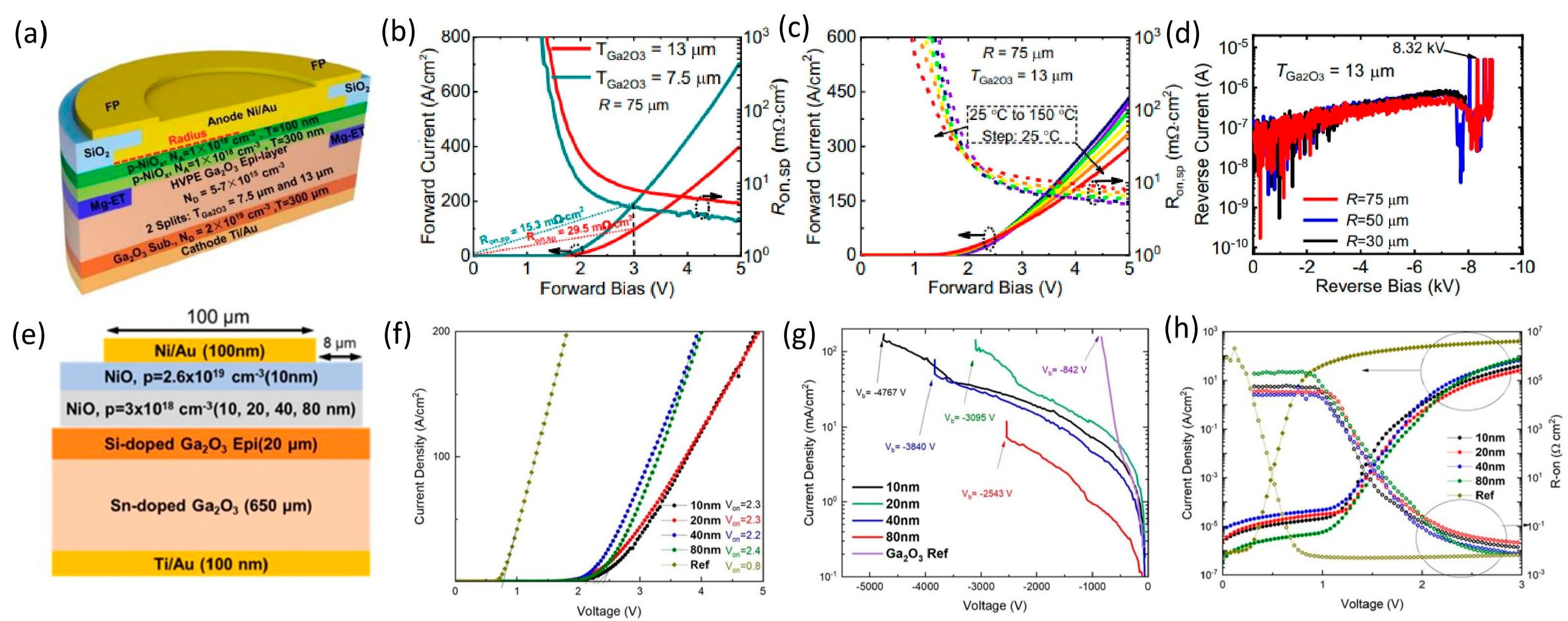
  47. Li, J.-S.; Chiang, C.-C.; Xia, X.; Yoo, T.J.; Ren, F.; Kim, H.; Pearton, S.J. Demonstration of 4.7 KV Breakdown Voltage in NiO/β-Ga2O3 Vertical Rectifiers. Appl. Phys. Lett. 2022, 121, 042105. [Google Scholar] [CrossRef]
  48. Attri, R.; Panda, D.P.; Ghatak, J.; Rao, C.N.R. High Crystalline Epitaxial Thin Films of NiO by Plasma-Enhanced ALD and Their Properties. APL Mater. 2023, 11, 091105. [Google Scholar] [CrossRef]
  49. Liao, C.; Lu, X.; Xu, T.; Fang, P.; Deng, Y.; Luo, H.; Wu, Z.; Chen, Z.; Liang, J.; Pei, Y.; et al. Optimization of NiO/β-Ga2O3 Heterojunction Diodes for High-Power Application. IEEE Trans. Electron Devices 2022, 69, 5722–5727. [Google Scholar] [CrossRef]
  50. Wrobel, F.; Park, H.; Sohn, C.; Hsiao, H.-W.; Zuo, J.-M.; Shin, H.; Lee, H.N.; Ganesh, P.; Benali, A.; Kent, P.R.C.; et al. Doped NiO: The Mottness of a Charge Transfer Insulator. Phys. Rev. B 2020, 101, 195128. [Google Scholar] [CrossRef]
  51. Luo, H.; Zhou, X.; Chen, Z.; Pei, Y.; Lu, X.; Wang, G. Fabrication and Characterization of High-Voltage NiO/β-Ga2O3 Heterojunction Power Diodes. IEEE Trans. Electron Devices 2021, 68, 3991–3996. [Google Scholar] [CrossRef]
  52. Gong, H.; Chen, X.; Xu, Y.; Chen, Y.; Ren, F.; Liu, B.; Gu, S.; Zhang, R.; Ye, J. Band Alignment and Interface Recombination in NiO/β-Ga2O3 Type-II p-n Heterojunctions. IEEE Trans. Electron Devices 2020, 67, 3341–3347. [Google Scholar] [CrossRef]
  53. Li, J.-S.; Wan, H.-H.; Chiang, C.-C.; Xia, X.; Yoo, T.J.; Kim, H.; Ren, F.; Pearton, S.J. Reproducible NiO/Ga2O3 Vertical Rectifiers with Breakdown Voltage >8 KV. Crystals 2023, 13, 886. [Google Scholar] [CrossRef]
  54. Deng, Y.; Yang, Z.; Xu, T.; Jiang, H.; Ng, K.W.; Liao, C.; Su, D.; Pei, Y.; Chen, Z.; Wang, G.; et al. Band Alignment and Electrical Properties of NiO/β-Ga2O3 Heterojunctions with Different β-Ga2O3 Orientations. Appl. Surf. Sci. 2023, 622, 156917. [Google Scholar] [CrossRef]
  55. Hao, W.; He, Q.; Zhou, K.; Xu, G.; Xiong, W.; Zhou, X.; Jian, G.; Chen, C.; Zhao, X.; Long, S. Low Defect Density and Small I−V Curve Hysteresis in NiO/β-Ga2O3 Pn Diode with a High PFOM of 0.65 GW/cm2. Appl. Phys. Lett. 2021, 118, 043501. [Google Scholar] [CrossRef]
  56. Yan, Q.; Gong, H.; Zhou, H.; Zhang, J.; Ye, J.; Liu, Z.; Wang, C.; Zheng, X.; Zhang, R.; Hao, Y. Low Density of Interface Trap States and Temperature Dependence Study of Ga2O3 Schottky Barrier Diode with P-NiOx Termination. Appl. Phys. Lett. 2022, 120, 092106. [Google Scholar] [CrossRef]
  57. Li, J.-S.; Wan, H.-H.; Chiang, C.-C.; Ren, F.; Pearton, S.J. Annealing Stability of NiO/Ga2O3 Vertical Heterojunction Rectifiers. Crystals 2023, 13, 1174. [Google Scholar] [CrossRef]
  58. Lu, X.; Zhou, X.; Jiang, H.; Ng, K.W.; Chen, Z.; Pei, Y.; Lau, K.M.; Wang, G. 1-KV Sputtered p-NiO/n-Ga2O3 Heterojunction Diodes with an Ultra-Low Leakage Current Below μA/cm2. IEEE Electron Device Lett. 2020, 41, 449–452. [Google Scholar] [CrossRef]
  59. Zhang, J.; Dong, P.; Dang, K.; Zhang, Y.; Yan, Q.; Xiang, H.; Su, J.; Liu, Z.; Si, M.; Gao, J.; et al. Ultra-Wide Bandgap Semiconductor Ga2O3 Power Diodes. Nat. Commun. 2022, 13, 3900. [Google Scholar] [CrossRef]
  60. Chiang, C.-C.; Li, J.-S.; Wan, H.-H.; Ren, F.; Pearton, S.J. The Optimization of NiO Doping, Thickness, and Extension in KV-Class NiO/Ga2O3 Vertical Rectifiers. Crystals 2023, 13, 1124. [Google Scholar] [CrossRef]
  61. Li, J.-S.; Chiang, C.-C.; Xia, X.; Wan, H.-H.; Ren, F.; Pearton, S.J. 1 Mm2, 3.6 KV, 4.8 A NiO/Ga2O3 Heterojunction Rectifiers. ECS J. Solid State Sci. Technol. 2023, 12, 085001. [Google Scholar] [CrossRef]
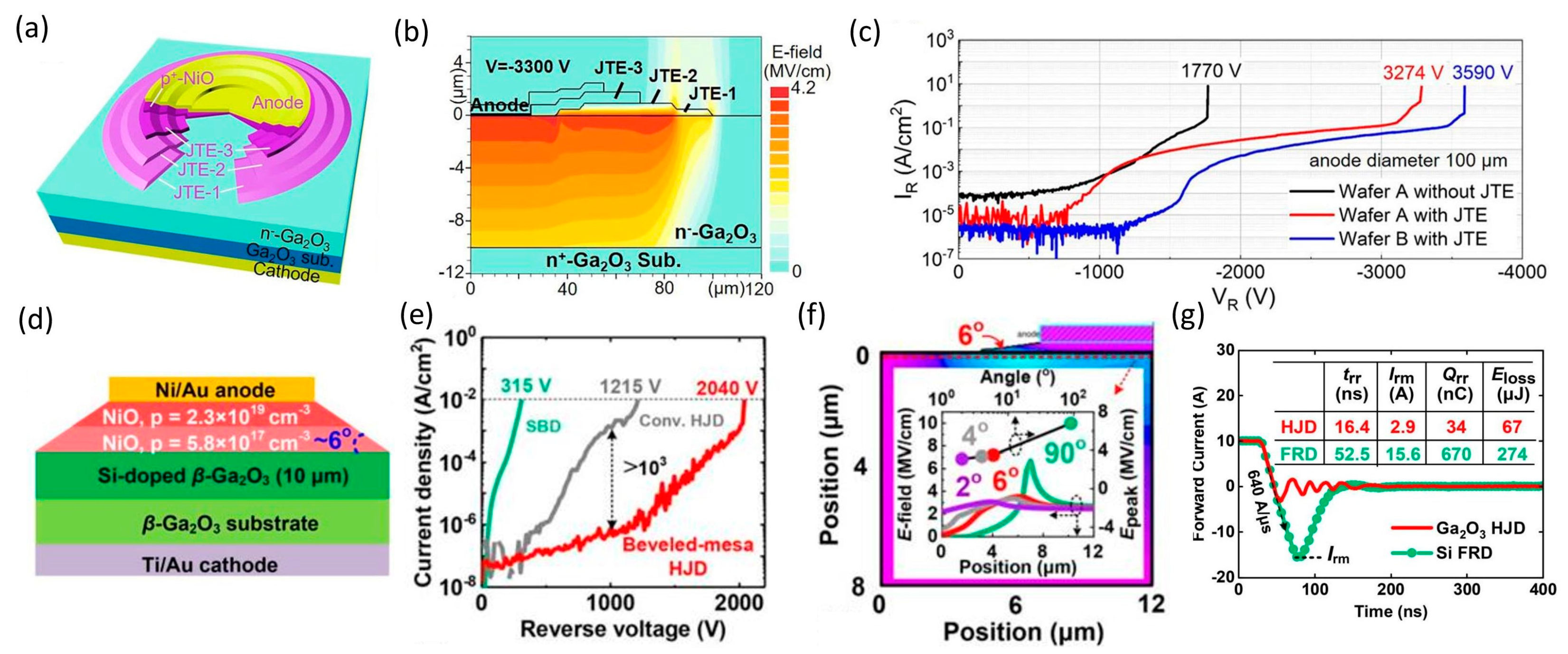
  62. Xiao, M.; Wang, B.; Spencer, J.; Qin, Y.; Porter, M.; Ma, Y.; Wang, Y.; Sasaki, K.; Tadjer, M.; Zhang, Y. NiO Junction Termination Extension for High-Voltage (>3 kV) Ga2O3 Devices. Appl. Phys. Lett. 2023, 122, 183501. [Google Scholar] [CrossRef]
  63. Zhou, F.; Gong, H.H.; Wang, Z.P.; Xu, W.Z.; Yu, X.X.; Yang, Y.; Ren, F.-F.; Gu, S.L.; Zhang, R.; Zheng, Y.D.; et al. Over 1.8 GW/cm2 Beveled-Mesa NiO/β-Ga2O3 Heterojunction Diode with 800 V/10 A Nanosecond Switching Capability. Appl. Phys. Lett. 2021, 119, 262103. [Google Scholar] [CrossRef]
  64. Hao, W.; He, Q.; Zhou, X.; Zhao, X.; Xu, G.; Long, S. 2.6 KV NiO/Ga2O3 Heterojunction Diode with Superior High-Temperature Voltage Blocking Capability. In Proceedings of the 2022 IEEE 34th International Symposium on Power Semiconductor Devices and ICs (ISPSD), Vancouver, BC, Canada, 22–25 May 2022; pp. 105–108. [Google Scholar]
  65. Wang, Y.; Gong, H.; Lv, Y.; Fu, X.; Dun, S.; Han, T.; Liu, H.; Zhou, X.; Liang, S.; Ye, J.; et al. 2.41 KV Vertical P-Nio/n-Ga2O3 Heterojunction Diodes with a Record Baliga’s Figure-of-Merit of 5.18 GW/cm2. IEEE Trans. Power Electron 2022, 37, 3743–3746. [Google Scholar] [CrossRef]
  66. Gong, H.H.; Chen, X.H.; Xu, Y.; Ren, F.-F.; Gu, S.L.; Ye, J.D. A 1.86-KV Double-Layered NiO/β-Ga2O3 Vertical p–n Heterojunction Diode. Appl. Phys. Lett. 2020, 117, 022104. [Google Scholar] [CrossRef]
  67. Li, J.-S.; Chiang, C.-C.; Xia, X.; Wan, H.-H.; Ren, F.; Pearton, S.J. 7.5 KV, 6.2 GW cm−2 NiO/β-Ga2O3 Vertical Rectifiers with on–off Ratio Greater than 1013. J. Vac. Sci. Technol. A 2023, 41, 030401. [Google Scholar] [CrossRef]
  68. Wang, B.; Xiao, M.; Spencer, J.; Qin, Y.; Sasaki, K.; Tadjer, M.J.; Zhang, Y. 2.5 KV Vertical Ga2O3 Schottky Rectifier with Graded Junction Termination Extension. IEEE Electron Device Lett. 2023, 44, 221–224. [Google Scholar] [CrossRef]
  69. Gong, H.H.; Yu, X.X.; Xu, Y.; Chen, X.H.; Kuang, Y.; Lv, Y.J.; Yang, Y.; Ren, F.-F.; Feng, Z.H.; Gu, S.L.; et al. β-Ga2O3 Vertical Heterojunction Barrier Schottky Diodes Terminated with p-NiO Field Limiting Rings. Appl. Phys. Lett. 2021, 118, 202102. [Google Scholar] [CrossRef]
  70. Wang, Y.; Gong, H.; Jia, X.; Han, G.; Ye, J.; Liu, Y.; Hu, H.; Ou, X.; Ma, X.; Hao, Y. First Demonstration of RESURF and Superjunction ß-Ga2O3 MOSFETs with p-NiO/n-Ga2O3 Junctions. In Proceedings of the 2021 IEEE International Electron Devices Meeting (IEDM), San Francisco, CA, USA, 11–16 December 2021; pp. 36.6.1–36.6.4. [Google Scholar]
  71. Qin, Y.; Xiao, M.; Porter, M.; Ma, Y.; Spencer, J.; Du, Z.; Jacobs, A.G.; Sasaki, K.; Wang, H.; Tadjer, M.; et al. 10-KV Ga2O3 Charge-Balance Schottky Rectifier Operational at 200 °C. IEEE Electron Device Lett. 2023, 44, 1268–1271. [Google Scholar] [CrossRef]
  72. Lv, Y.; Wang, Y.; Fu, X.; Dun, S.; Sun, Z.; Liu, H.; Zhou, X.; Song, X.; Dang, K.; Liang, S.; et al. Demonstration of β-Ga2O3 Junction Barrier Schottky Diodes with a Baliga’s Figure of Merit of 0.85 GW/cm2 or a 5A/700 V Handling Capabilities. IEEE Trans. Power Electron 2021, 36, 6179–6182. [Google Scholar] [CrossRef]
  73. Yan, Q.; Gong, H.; Zhang, J.; Ye, J.; Zhou, H.; Liu, Z.; Xu, S.; Wang, C.; Hu, Z.; Feng, Q.; et al. β-Ga2O3 Hetero-Junction Barrier Schottky Diode with Reverse Leakage Current Modulation and BV2/Ron,Sp Value of 0.93 GW/cm2. Appl. Phys. Lett. 2021, 118, 122102. [Google Scholar] [CrossRef]
  74. Wu, F.; Wang, Y.; Jian, G.; Xu, G.; Zhou, X.; Guo, W.; Du, J.; Liu, Q.; Dun, S.; Yu, Z.; et al. Superior Performance β-Ga2O3 Junction Barrier Schottky Diodes Implementing p-NiO Heterojunction and Beveled Field Plate for Hybrid Cockcroft–Walton Voltage Multiplier. IEEE Trans. Electron Devices 2023, 70, 1199–1205. [Google Scholar] [CrossRef]
  75. Wang, C.; Gong, H.; Lei, W.; Cai, Y.; Hu, Z.; Xu, S.; Liu, Z.; Feng, Q.; Zhou, H.; Ye, J.; et al. Demonstration of the P-NiOx/n-Ga2O3 Heterojunction Gate FETs and Diodes with BV2/Ron,Sp Figures of Merit of 0.39 GW/cm2 and 1.38 GW/cm2. IEEE Electron Device Lett. 2021, 42, 485–488. [Google Scholar] [CrossRef]
  76. Zhou, X.; Liu, Q.; Hao, W.; Xu, G.; Long, S. Normally-off β-Ga2O3 Power Heterojunction Field-Effect-Transistor Realized by p-NiO and Recessed-Gate. In Proceedings of the 2022 IEEE 34th International Symposium on Power Semiconductor Devices and ICs (ISPSD), Vancouver, BC, Canada, 22–25 May 2022; pp. 101–104. [Google Scholar]
  77. Ashwin Kumar Saikumar, S.D.N.; Sundaram, K.B. A Review of Recent Developments in Aluminum Gallium Oxide Thin Films and Devices. Crit. Rev. Solid State Mater. Sci. 2022, 47, 538–569. [Google Scholar] [CrossRef]
  78. Ranga, P.; Rishinaramangalam, A.; Varley, J.; Bhattacharyya, A.; Feezell, D.; Krishnamoorthy, S. Si-Doped β-(Al0.26Ga0.74)2O3 Thin Films and Heterostructures Grown by Metalorganic Vapor-Phase Epitaxy. Appl. Phys. Express 2019, 12, 111004. [Google Scholar] [CrossRef]
  79. Okumura, H.; Kato, Y.; Oshima, T.; Palacios, T. Demonstration of Lateral Field-Effect Transistors Using Sn-Doped β-(AlGa)2O3 (010). Jpn. J. Appl. Phys. 2019, 58, SBBD12. [Google Scholar] [CrossRef]
  80. Peelaers, H.; Varley, J.B.; Speck, J.S.; Van de Walle, C.G. Structural and electronic properties of Ga2O3-Al2O3 alloys. Appl. Phys. Lett. 2018, 112, 242101. [Google Scholar] [CrossRef]
  81. Zhang, F.; Saito, K.; Tanaka, T.; Nishio, M.; Arita, M.; Guo, Q. Wide Bandgap Engineering of (AlGa)2O3 Films. Appl. Phys. Lett. 2014, 105, 162107. [Google Scholar] [CrossRef]
  82. Wang, C.-C.; Yuan, S.-H.; Ou, S.-L.; Huang, S.-Y.; Lin, K.-Y.; Chen, Y.-A.; Hsiao, P.-W.; Wuu, D.-S. Growth and Characterization of Co-Sputtered Aluminum-Gallium Oxide Thin Films on Sapphire Substrates. J. Alloys Compd. 2018, 765, 894–900. [Google Scholar] [CrossRef]
  83. Oshima, T.; Okuno, T.; Arai, N.; Kobayashi, Y.; Fujita, S. β-Al2xGa2-2xO3 Thin Film Growth by Molecular Beam Epitaxy. Jpn. J. Appl. Phys. 2009, 48, 070202. [Google Scholar] [CrossRef]
  84. Oshima, Y.; Ahmadi, E.; Badescu, S.C.; Wu, F.; Speck, J.S. Composition Determination of β-(AlxGa1−x)2O3 Layers Coherently Grown on (010) β-Ga2O3 Substrates by High-Resolution X-Ray Diffraction. Appl. Phys. Express 2016, 9, 061102. [Google Scholar] [CrossRef]
  85. Kaun, S.W.; Wu, F.; Speck, J.S. β-(AlxGa1−x)2O3/Ga2O3 (010) Heterostructures Grown on β-Ga2O3 (010) Substrates by Plasma-Assisted Molecular Beam Epitaxy. J. Vac. Sci. Technol. A 2015, 33, 041508. [Google Scholar] [CrossRef]
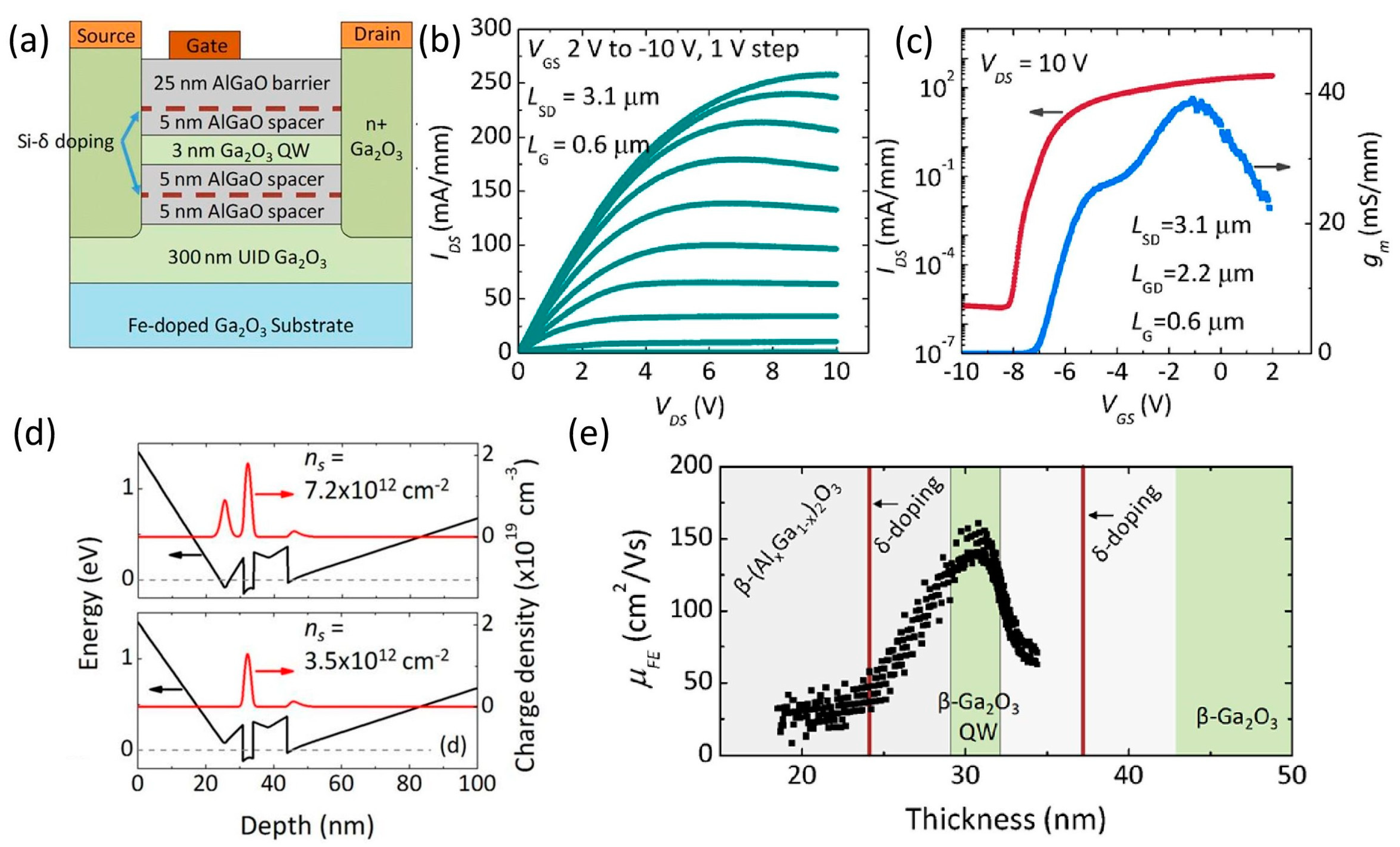
  86. Zhang, Y.; Neal, A.; Xia, Z.; Joishi, C.; Johnson, J.M.; Zheng, Y.; Bajaj, S.; Brenner, M.; Dorsey, D.; Chabak, K.; et al. Demonstration of High Mobility and Quantum Transport in Modulation-Doped β-(AlxGa1−x)2O3/Ga2O3 Heterostructures. Appl. Phys. Lett. 2018, 112, 173502. [Google Scholar] [CrossRef]
  87. Miller, R.; Alema, F.; Osinsky, A. Epitaxial β-Ga2O3 and β-(AlxGa1−x)2O3/β-Ga2O3 Heterostructures Growth for Power Electronics. IEEE Trans. Semicond. Manuf. 2018, 31, 467–474. [Google Scholar] [CrossRef]
  88. Zhang, Y.; Mauze, A.; Speck, J.S. Development of β-(AlxGa1−x)2O3/Ga2O3 Heterostructures; University of California: Santa Barbara CA, USA, 2019. [Google Scholar]
  89. Bhuiyan, A.F.M.A.U.; Meng, L.; Huang, H.-L.; Chae, C.; Hwang, J.; Zhao, H. Al Incorporation up to 99% in Metalorganic Chemical Vapor Deposition-Grown Monoclinic (AlxGa1−x)2O3 Films Using Trimethylgallium. Phys. Status Solidi (RRL)–Rapid Res. Lett. 2023, 17, 2300224. [Google Scholar] [CrossRef]
  90. Wang, D.; Mudiyanselage, D.H.; Fu, H. Design Space of Delta-Doped β-(AlxGa1-x)2O3/Ga2O3 High-Electron Mobility Transistors. IEEE Trans. Electron Devices 2022, 69, 69–74. [Google Scholar] [CrossRef]
  91. Ahmadi, E.; Koksaldi, O.S.; Zheng, X.; Mates, T.; Oshima, Y.; Mishra, U.K.; Speck, J.S. Demonstration of β-(AlxGa1−x)2O3/β-Ga2O3 Modulation Doped Field-Effect Transistors with Ge as Dopant Grown via Plasma-Assisted Molecular Beam Epitaxy. Appl. Phys. Express 2017, 10, 071101. [Google Scholar] [CrossRef]
  92. Kalarickal, N.K.; Xia, Z.; McGlone, J.F.; Liu, Y.; Moore, W.; Arehart, A.R.; Ringel, S.A.; Rajan, S. High Electron Density β-(Al0.17Ga0.83)2O3/Ga2O3 Modulation Doping Using an Ultra-Thin (1 Nm) Spacer Layer. J. Appl. Phys. 2020, 127, 215706. [Google Scholar] [CrossRef]
  93. Kalarickal, N.K.; Feng, Z.; Anhar Uddin Bhuiyan, A.F.M.; Xia, Z.; Moore, W.; McGlone, J.F.; Arehart, A.R.; Ringel, S.A.; Zhao, H.; Rajan, S. Electrostatic Engineering Using Extreme Permittivity Materials for Ultra-Wide Bandgap Semiconductor Transistors. IEEE Trans. Electron Devices 2021, 68, 29–35. [Google Scholar] [CrossRef]
  94. Zhang, Y.; Joishi, C.; Xia, Z.; Brenner, M.; Lodha, S.; Rajan, S. Demonstration of β-(AlxGa1−x)2O3/Ga2O3 Double Heterostructure Field Effect Transistors. Appl. Phys. Lett. 2018, 112, 233503. [Google Scholar] [CrossRef]
  95. Kalarickal, N.K.; Xia, Z.; Huang, H.-L.; Moore, W.; Liu, Y.; Brenner, M.; Hwang, J.; Rajan, S. β-(Al0.18Ga0.82)2O3/Ga2O3 Double Heterojunction Transistor with Average Field of 5.5 MV/Cm. IEEE Electron Device Lett. 2021, 42, 899–902. [Google Scholar] [CrossRef]
  96. Vaidya, A.; Saha, C.N.; Singisetti, U. Enhancement Mode β-(AlxGa1−x)2O3/Ga2O3 Heterostructure FET (HFET) with High Transconductance and Cutoff Frequency. IEEE Electron Device Lett. 2021, 42, 1444–1447. [Google Scholar] [CrossRef]
  97. Joishi, C.; Zhang, Y.; Xia, Z.; Sun, W.; Arehart, A.R.; Ringel, S.; Lodha, S.; Rajan, S. Breakdown Characteristics of β-(Al0.22Ga0.78)2O3/Ga2O3 Field-Plated Modulation-Doped Field-Effect Transistors. IEEE Electron Device Lett. 2019, 40, 1241–1244. [Google Scholar] [CrossRef]
  98. Wang, D.; Mudiyanselage, D.H.; Fu, H. Design of KV-Class and Low RON E-Mode β-Ga2O3 Current Aperture Vertical Transistors with Delta-Doped β-(AlxGa1−x)2O3/Ga2O3 Heterostructure. IEEE Trans. Electron Devices 2023, 70, 5795–5802. [Google Scholar] [CrossRef]
  99. Sundaram, P.P.; Alema, F.; Osinsky, A.; Koester, S.J. β-(AlxGa1−x)2O3/Ga2O3 Heterostructure Schottky Diodes for Improved VBR2/RON. J. Vac. Sci. Technol. A 2022, 40, 043211. [Google Scholar] [CrossRef]
  100. Ahmadi, E.; Oshima, Y.; Wu, F.; Speck, J.S. Schottky Barrier Height of Ni to β-(AlxGa1−x)2O3 with Different Compositions Grown by Plasma-Assisted Molecular Beam Epitaxy. Semicond. Sci. Technol. 2017, 32, 035004. [Google Scholar] [CrossRef]
  101. Mudiyanselage, D.H.; Wang, D.; Fu, H. Ultrawide Bandgap Vertical β-(AlxGa1−x)2O3 Schottky Barrier Diodes on Free-Standing β-Ga2O3 Substrates. J. Vac. Sci. Technol. A 2023, 41, 023201. [Google Scholar] [CrossRef]
  102. Wan, H.-H.; Li, J.-S.; Chiang, C.-C.; Xia, X.; Ren, F.; Masten, H.N.; Lundh, J.S.; Spencer, J.A.; Alema, F.; Osinsky, A.; et al. Operation of NiO/β-(Al0.21Ga0.79)2O3/Ga2O3 Heterojunction Lateral Rectifiers at up to 225 °C. ECS J. Solid State Sci. Technol. 2023, 12, 075008. [Google Scholar] [CrossRef]
  103. Wan, H.-H.; Li, J.-S.; Chiang, C.-C.; Xia, X.; Ren, F.; Masten, H.N.; Lundh, J.S.; Spencer, J.A.; Alema, F.; Osinsky, A.; et al. NiO/β-(AlxGa1−x)2O3/Ga2O3 Heterojunction Lateral Rectifiers with Reverse Breakdown Voltage >7 kV. J. Vac. Sci. Technol. A 2023, 41, 032701. [Google Scholar] [CrossRef]
  104. Montes, J.; Yang, C.; Fu, H.; Yang, T.-H.; Fu, K.; Chen, H.; Zhou, J.; Huang, X.; Zhao, Y. Demonstration of Mechanically Exfoliated β-Ga2O3/GaN p-n Heterojunction. Appl. Phys. Lett. 2019, 114, 162103. [Google Scholar] [CrossRef]
  105. Herath Mudiyanselage, D.; Wang, D.; Fu, H. Wide Bandgap Vertical KV-Class β-Ga2O3/GaN Heterojunction p-n Power Diodes with Mesa Edge Termination. IEEE J. Electron Devices Soc. 2022, 10, 89–97. [Google Scholar] [CrossRef]
  106. Nandi, A.; Rana, K.S.; Bag, A. Design and Analysis of P-GaN/N-Ga2O3 Based Junction Barrier Schottky Diodes. IEEE Trans. Electron Devices 2021, 68, 6052–6058. [Google Scholar] [CrossRef]
  107. Mudiyanselage, D.H.; Wang, D.; Fu, H. Design and Analysis of KV-Class Ultrawide Bandgap β-Ga2O3/p-GaN Heterojunction Barrier Schottky Diodes. In Proceedings of the 2022 Compound Semiconductor Week (CSW), Ann Arbor, MI, USA, 1–3 June 2022; pp. 1–2. [Google Scholar]
  108. Nakagomi, S.; Momo, T.; Takahashi, S.; Kokubun, Y. Deep Ultraviolet Photodiodes Based on β-Ga2O3/SiC Heterojunction. Appl. Phys. Lett. 2013, 103, 072105. [Google Scholar] [CrossRef]
  109. Nakagomi, S.; Hiratsuka, K.; Kakuda, Y.; Yoshihiro, K. Beta-Gallium Oxide/SiC Heterojunction Diodes with High Rectification Ratios. ECS J. Solid State Sci. Technol. 2016, 6, Q3030. [Google Scholar] [CrossRef]
  110. Song, Y.; Bhattacharyya, A.; Karim, A.; Shoemaker, D.; Huang, H.-L.; Roy, S.; McGray, C.; Leach, J.H.; Hwang, J.; Krishnamoorthy, S.; et al. Ultra-Wide Band Gap Ga2O3-on-SiC MOSFETs. ACS Appl. Mater. Interfaces 2023, 15, 7137–7147. [Google Scholar] [CrossRef]
  111. Watahiki, T.; Yuda, Y.; Furukawa, A.; Yamamuka, M.; Takiguchi, Y.; Miyajima, S. Heterojunction P-Cu2O/n-Ga2O3 Diode with High Breakdown Voltage. Appl. Phys. Lett. 2017, 111, 222104. [Google Scholar] [CrossRef]
  112. Gallagher, J.C.; Koehler, A.D.; Tadjer, M.J.; Mahadik, N.A.; Anderson, T.J.; Budhathoki, S.; Law, K.-M.; Hauser, A.J.; Hobart, K.D.; Kub, F.J. Demonstration of CuI as a P–N Heterojunction to β-Ga2O3. Appl. Phys. Express 2019, 12, 104005. [Google Scholar] [CrossRef]
  113. Budde, M.; Splith, D.; Mazzolini, P.; Tahraoui, A.; Feldl, J.; Ramsteiner, M.; von Wenckstern, H.; Grundmann, M.; Bierwagen, O. SnO/β-Ga2O3 Vertical Pn Heterojunction Diodes. Appl. Phys. Lett. 2020, 117, 252106. [Google Scholar] [CrossRef]
  114. Tetzner, K.; Egbo, K.; Klupsch, M.; Unger, R.-S.; Popp, A.; Chou, T.-S.; Anooz, S.B.; Galazka, Z.; Trampert, A.; Bierwagen, O.; et al. SnO/β-Ga2O3 Heterojunction Field-Effect Transistors and Vertical p–n Diodes. Appl. Phys. Lett. 2022, 120, 112110. [Google Scholar] [CrossRef]
  115. Umezawa, H. Recent Advances in Diamond Power Semiconductor Devices. Mater. Sci. Semicond. Process 2018, 78, 147–156. [Google Scholar] [CrossRef]
  116. Isberg, J.; Hammersberg, J.; Johansson, E.; Wikström, T.; Twitchen, D.J.; Whitehead, A.J.; Coe, S.E.; Scarsbrook, G.A. High Carrier Mobility in Single-Crystal Plasma-Deposited Diamond. Science 2002, 297, 1670–1672. [Google Scholar] [CrossRef] [PubMed]
  117. Sittimart, P.; Ohmagari, S.; Matsumae, T.; Umezawa, H.; Yoshitake, T. Diamond/β-Ga2O3 Pn Heterojunction Diodes Fabricated by Low-Temperature Direct-Bonding. AIP Adv. 2021, 11, 105114. [Google Scholar] [CrossRef]
  118. Matsumae, T.; Kurashima, Y.; Umezawa, H.; Tanaka, K.; Ito, T.; Watanabe, H.; Takagi, H. Low-Temperature Direct Bonding of β-Ga2O3 and Diamond Substrates under Atmospheric Conditions. Appl. Phys. Lett. 2020, 116, 141602. [Google Scholar] [CrossRef]
  119. Nandi, A.; Cherns, D.; Sanyal, I.; Kuball, M. Epitaxial Growth of (−201) β-Ga2O3 on (001) Diamond Substrates. Cryst. Growth Des. 2023, 23, 8290–8295. [Google Scholar] [CrossRef] [PubMed]
  120. Kusaba, T.; Sittimart, P.; Katamune, Y.; Kageura, T.; Naragino, H.; Ohmagari, S.; Valappil, S.M.; Nagano, S.; Zkria, A.; Yoshitake, T. Heteroepitaxial Growth of β-Ga2O3 Thin Films on Single Crystalline Diamond (111) Substrates by Radio Frequency Magnetron Sputtering. Appl. Phys. Express 2023, 16, 105503. [Google Scholar] [CrossRef]
  121. Mishra, A.; Abdallah, Z.; Pomeroy, J.W.; Uren, M.J.; Kuball, M. Electrical and Thermal Performance of Ga2O3–Al2O3–Diamond Super-Junction Schottky Barrier Diodes. IEEE Trans. Electron Devices 2021, 68, 5055–5061. [Google Scholar] [CrossRef]
  122. Malakoutian, M.; Song, Y.; Yuan, C.; Ren, C.; Lundh, J.S.; Lavelle, R.M.; Brown, J.E.; Snyder, D.W.; Graham, S.; Choi, S.; et al. Polycrystalline Diamond Growth on β-Ga2O3 for Thermal Management. Appl. Phys. Express 2021, 14, 55502. [Google Scholar] [CrossRef]
  123. Rahaman, I.; Ellis, H.D.; Fu, K. Robust Diamond/{eta}-Ga2O3 Hetero-p-n-Junction Via Mechanically Integrating Their Building Blocks. arXiv 2023, arXiv:2311.16323. [Google Scholar]
  124. Hickman, A.L.; Chaudhuri, R.; Bader, S.J.; Nomoto, K.; Li, L.; Hwang, J.C.M.; Xing, H.G.; Jena, D. Next Generation Electronics on the Ultrawide-Bandgap Aluminum Nitride Platform. Semicond. Sci. Technol. 2021, 36, 44001. [Google Scholar] [CrossRef]
  125. Chen, J.-X.; Tao, J.-J.; Ma, H.-P.; Zhang, H.; Feng, J.-J.; Liu, W.-J.; Xia, C.; Lu, H.-L.; Zhang, D.W. Band Alignment of AlN/β-Ga2O3 Heterojunction Interface Measured by x-Ray Photoelectron Spectroscopy. Appl. Phys. Lett. 2018, 112, 261602. [Google Scholar] [CrossRef]
  126. Song, K.; Zhang, H.; Fu, H.; Yang, C.; Singh, R.; Zhao, Y.; Sun, H.; Long, S. Normally-off AlN/β-Ga2O3 Field-Effect Transistors Using Polarization-Induced Doping. J. Phys. D Appl. Phys. 2020, 53, 345107. [Google Scholar] [CrossRef]
  127. Baskaran, S.; Shunmugathammal, M.; Sivamani, C.; Ravi, S.; Murugapandiyan, P.; Ramkumar, N. UWBG AlN/β-Ga2O3 HEMT on Silicon Carbide Substrate for Low Loss Portable Power Converters and RF Applications. Silicon 2022, 14, 11079–11087. [Google Scholar] [CrossRef]
  128. He, Z.; Fu, K.; Xu, M.; Zhou, J.; Li, T.; Zhao, Y. Understanding the Breakdown Behavior of Ultrawide-Bandgap Boron Nitride Power Diodes Using Device Modeling. Phys. Status Solidi (RRL)–Rapid Res. Lett. 2023, 2200397. [Google Scholar] [CrossRef]
  129. Biswas, A.; Xu, M.; Fu, K.; Zhou, J.; Xu, R.; Puthirath, A.B.; Hachtel, J.A.; Li, C.; Iyengar, S.A.; Kannan, H.; et al. Properties and Device Performance of BN Thin Films Grown on GaN by Pulsed Laser Deposition. Appl. Phys. Lett. 2022, 121, 092105. [Google Scholar] [CrossRef]
  130. Xu, M.; Biswas, A.; Li, T.; He, Z.; Luo, S.; Mei, Z.; Zhou, J.; Chang, C.; Puthirath, A.B.; Vajtai, R.; et al. Vertical β-Ga2O3 Metal–Insulator–Semiconductor Diodes with an Ultrathin Boron Nitride Interlayer. Appl. Phys. Lett. 2023, 123, 232107. [Google Scholar] [CrossRef]
  131. Lemme, M.C.; Akinwande, D.; Huyghebaert, C.; Stampfer, C. 2D Materials for Future Heterogeneous Electronics. Nat. Commun. 2022, 13, 1392. [Google Scholar] [CrossRef]
  132. Su, S.-K.; Chuu, C.-P.; Li, M.-Y.; Cheng, C.-C.; Wong, H.-S.P.; Li, L.-J. Layered Semiconducting 2D Materials for Future Transistor Applications. Small Struct. 2021, 2, 2000103. [Google Scholar] [CrossRef]
  133. Yan, X.; Esqueda, I.S.; Ma, J.; Tice, J.; Wang, H. High Breakdown Electric Field in β-Ga2O3/Graphene Vertical Barristor Heterostructure. Appl. Phys. Lett. 2018, 112, 032101. [Google Scholar] [CrossRef]
  134. Kim, J.; Mastro, M.A.; Tadjer, M.J.; Kim, J. Heterostructure WSe2−Ga2O3 Junction Field-Effect Transistor for Low-Dimensional High-Power Electronics. ACS Appl. Mater. Interfaces 2018, 10, 29724–29729. [Google Scholar] [CrossRef] [PubMed]
  135. Leblanc, C.; Herath Mudiyanselage, D.; Song, S.; Zhang, H.; Davydov, A.V.; Fu, H.; Jariwala, D. Vertical van Der Waals Heterojunction Diodes Comprising 2D Semiconductors on 3D β-Ga2O3. Nanoscale 2023, 15, 9964–9972. [Google Scholar] [CrossRef] [PubMed]
Figure 1. (a) Band alignment of NiOx/β-Ga2O3 with annealing at varying temperatures (up to 600 °C). (b) X-ray photoelectron spectroscopy (XPS) spectra illustrating the composition of deposited NiOx. (c) X-ray diffraction (XRD) pattern of NiOx at different annealing temperatures. (d) Variation in O/Ni and Ni2O3/NiO ratios and (e) variation in bandgap and resistivity achieved by changing the O2/Ar gas flow. (f) Variation in bandgap and Ni2O3/NiO ratio with annealing temperature. (a) reproduced with permission from X. Xia et al., J. Phys. D: Appl. Phys. 55, 385105 (2022) [45]. Copyright 2022 IOP Publishing. (bf) reproduced with permission from J.-S. Li et al., J. Vac. Sci. Technol. A 41, 013405 (2022) [41]. Copyright 2022 American Vacuum Society.
Electronics 13 01234 g001
Figure 2. (a) Band alignment and interface recombination at low bias (<~1.5 V) and (b) multi-step tunneling at high bias (>1.5 V) in a NiOx/β-Ga2O3 p-n diode. (c) Transmission electron microscope (TEM) image of a fabricated p-n diode encompassing all regions. (d) The p-n diode interface with a sputtered NiOx layer, with the blue arrow indicating some interface deformation due to the involvement of high-energy plasma (150 W). (e) Low-power sputtered heterojunction with minimal damage to the interface (70 W). (f) E-beam-deposited p-n diode featuring an abrupt interface. (c,d) reproduced with permission from J.-S. Li et al., Appl. Phys. Lett. 121, 042105 (2022) [47]. Copyright 2022 AIP Publishing. (e) reproduced with permission from J.-S. Li et al., Crystals (Basel) 13, 886 (2023) [53]. Copyright 2023 under the terms of CC BY 4.0. (f) reproduced with permission from D. H. Mudiyanselage et al., Appl. Phys. Express 16, 094002 (2023) [43]. Copyright 2023 IOP Publishing.
Electronics 13 01234 g002
Figure 3. (a) A p-n diode with an 8.32 kV BV. (b) Forward I–V and Ron,sp of devices with 7.5 and 13 µm drift layers. (c) Temperature-dependent forward I–V and Ron,sp. (d) Reverse BV curve of the device with a 13 µm drift layer with different-diameter Ohmic contacts. (e) A 4.7 kV BV p-n diode. (f) Forward I–V and (g) reverse BV of demonstrated devices. (h) Forward I–V and Ron,sp on log scale. (ad) reproduced with permission from J. Zhang et al., Nat. Commun. 13, 3900 (2022) [59]. Copyright 2022 under the terms of CC BY 4.0. (eh) reproduced with permission from J.-S. Li et al., Appl. Phys. Lett. 121, 042105 (2022) [47]. Copyright 2022 AIP Publishing.
Electronics 13 01234 g003
Figure 4. (a) A NiOx/β-Ga2O3 p-n diode with multiple JTEs of various lengths. (b) Electric field profile of the device with 3.3 kV reverse bias. (c) BV curves of devices with and without JTEs. (d) A 2.04 kV p-n diode with beveled mesa edge termination. (e) BV comparison of SBD, heterojunction diode, and beveled mesa heterojunction diode. (f) Simulation of and reduction in electric field crowding with bevel angle. (g) Comparison of reverse recovery curves of NiOx/β-Ga2O3 heterojunction and Si FRD. (ac) reproduced with permission from M. Xiao et al., Appl. Phys. Lett. 122, 183501 (2023) [62]. Copyright 2023 AIP Publishing. (dg) F. Zhou et al., Appl. Phys. Lett. 119, 262103 (2021) [63]. Copyright 2021 AIP Publishing.
Electronics 13 01234 g004
Figure 5. (a) β-Ga2O3 SBD with a p-NiOx heterojunction edge termination and SiO2 FP. (b) Forward I–V and Ron,sp of devices with different diameters. (c) Forward I–V on log scale. (d) BV curves of devices with and without heterojunction and FP. (e) Schematic of SBD with and without FLRs. (f) Forward I–V of JBS, SBD, and SBD-FLR devices on a log scale. (g) Forward I–V on a linear scale and Ron,sp of devices. (h) BV curves of all demonstrated devices. (ad) reproduced with permission from Q. Yan et al., Appl. Phys. Lett. 120, 092106 (2022) [56]. Copyright 2022 AIP Publishing. (eh) H. H. Gong et al., Appl. Phys. Lett. 118, 202102 (2021) [69]. Copyright 2021 AIP Publishing.
Electronics 13 01234 g005
Figure 6. (a) A modulation-doped FET (MODFET) grown using MBE with Si modulation doping (δ-doping). (b) The HRXRD spectra of the grown films A and B. (c) A band diagram of the heterostructure and confinement of 2DEG. (d) The carrier density vs. temperature from Hall measurements. The measured and fitted mobility in samples (e) A and (f) B. (af) reproduced with permission from Y. Zhang et al., Appl. Phys. Lett. 112, 173502 (2018) [86]. Copyright 2018 AIP Publishing.
Electronics 13 01234 g006
Figure 7. (a) A HRXRD plot of β-(AlxGa1−x)2O3 epilayers grown using MOCVD (inset: the grown structure). (b) Carrier concentration and (c) mobility vs. temperature plots for three different samples, A, B, and C. (d) Fermi level separation from the conduction band with increasing temperature. (e) A HRXRD plot of β-(AlxGa1−x)2O3 epilayers grown on Sn-doped substrate (inset: the grown structure). (f) The carrier concentration versus depth profile extracted from C–V measurements. (g) The band diagram simulated from a Poisson–Schrödinger solver. (ag) reproduced with permission from P. Ranga et al., Appl. Phys. Express 12, 111004 (2019) [78]. Copyright 2019 IOP Publishing.
Electronics 13 01234 g007
Figure 8. (a) Schematic of a double heterostructure MODFET (DHFET). (b) Output and (c) transfer characteristics of demonstrated device. (d) Energy band diagrams with and without parallel conducting channels and the corresponding 2DEG charge distributions. (e) Depth profile vs. mobility of a demonstrated FET. (ae) reproduced with permission from Y. Zhang et al., Appl. Phys. Lett. 112, 233503 (2018) [94]. Copyright 2018 AIP Publishing.
Electronics 13 01234 g008
Figure 9. (a) Schematic of vertical β-(AlxGa1−x)2O3 SBD. (b) An HRXRD plot of the grown films with different Al compositions of x = 0, 0.038, 0.084, and 0.164. (c) Temperature-dependent I–V curves for x = 0.084 SBD. (d) The variation in Schottky barrier height and ideality factor with temperature as extracted from (c). (e) β-Ga2O3 SBD with a thin β-(AlxGa1−x)2O3 cap (x = 0.22). (f) Forward I–V characteristics on a log scale (inset: forward I–V characteristics on a linear scale). (g) The reverse breakdown of the capped and conventional SBDs. (h) The simulated electric field at the anode edge with and without β-(AlxGa1−x)2O3 cap. (i) A fabricated vertical β-(AlxGa1−x)2O3 SBD (x = 0.21). (j) Temperature-dependent I–V curves. (k) The variation in Schottky barrier height and ideality factor with temperature. (l) Reverse leakage mechanisms of the fabricated SBDs. (ad) E. Ahmadi et al., Semicond. Sci. Technol. 32, 035004 (2017) [100]. Copyright 2017 IOP Publishing. (eh) reproduced with permission from P. P. Sundaram et al., J. Vac. Sci. Technol. A 40, 043211 (2022) [99]. Copyright 2022 American Vacuum Society. (il): D.H. Mudiyanselage et al., J. Vac. Sci. Technol. A 41, 023201 (2023) [101]. Copyright 2023 American Vacuum Society.
Electronics 13 01234 g009
Figure 10. (a) Demonstrated NiOx/β-(Al0.21Ga0.79)2O3/β-Ga2O3 heterojunction lateral p-n diode. (b) Temperature-dependent forward I–V and Ron,sp on a log scale. (c) Temperature-dependent I–V characteristics on a linear scale and extracted turn-on voltages. (d) Variation in BV with temperature. (ad) reproduced with permission from H.-H. Wan et al., ECS J. Solid State Sci. Technol. 12, 075008 (2023) [102]. Copyright 2023 under the terms of CC BY 4.0.
Electronics 13 01234 g010
Figure 11. (a) Process of mechanical exfoliation and forming the p-GaN/β-Ga2O3 p-n diodes. (b) The forward I–V curve on a linear scale (inset: forward I–V curve on a log scale). (c) Comparison of forward I–V between the SBD and p-n diode on a linear scale (inset: forward I–V curves on a log scale). (d) Temperature-dependent I–V curves. (e) The variation in ideality factor and turn-on voltage of the device with temperature. (f) Simulated band diagram of the p-n heterojunction. (g) Variation in turn-on voltage in fabricated devices. (h) Arrhenius plot of a device at 3.5 V forward bias. (i) Forward I–V curves for β-Ga2O3 with different thicknesses. (ai) reproduced with permission from J. Montes et al., Appl. Phys. Lett. 114, 162103 (2019) [104]. Copyright 2019 AIP Publishing.
Electronics 13 01234 g011
Figure 12. (a) Schematics of Cu2O/β-Ga2O3 p-n diode and Pt/β-Ga2O3 SBD. (b) Band alignment of Cu2O/β-Ga2O3 heterojunction. (c) Forward and (d) reverse I–V characteristics of the p-n diode and SBD. (e) Schematic of the vertical SnO/β-Ga2O3 heterojunction diodes. (f) Band diagram of SnO/β-Ga2O3 heterojunction. (g) Temperature-dependent I–V characteristics of SnO/β-Ga2O3 p-n diode on a log scale (inset: variation in barrier height with temperature). (h) 1/C2–V measurements of two p-n diodes. (i) Schematic of SnO/β-Ga2O3 HJFET. (j) Transfer and (k) output characteristics of the fabricated SnO/β-Ga2O3 HJFET with LGD = 4 µm. (l) Off-state breakdown of the HJFET. (ad) reproduced with permission from T. Watahiki et al., Appl. Phys. Lett. 111, 222104 (2017) [111]. Copyright 2017 AIP Publishing. (eh) reproduced with permission from M. Budde et al., Appl. Phys. Lett. 117, 252106 (2020) [113]. Copyright 2020 AIP Publishing. (il) reproduced with permission from K. Tetzner et al., Appl. Phys. Lett. 120, 112110 (2022) [114]. Copyright 2022 AIP Publishing.
Electronics 13 01234 g012
Figure 13. (a) Forward I–V characteristics of a diamond/β-Ga2O3 p-n diode (inset: demonstrated p-n diode with thermal bonding). (b) The simulated band diagram. (c) Forward I–V of characteristics a SBD and a p-n diode. (d) C–V measurements of a p-n diode. (e) Mechanically integrated diamond/β-Ga2O3 p-n diode. (f) Temperature-dependent forward I–V curves on a linear scale. (g) Temperature-dependent forward I–V curve and the ideality factor on a log scale. (ad) reproduced with permission from P. Sittimart et al., AIP. Adv. 11, 105114 (2021) [117]. Copyright 2021 under the terms of CC BY 4.0. (eg) reproduced from I. Rahaman et al., arXiv:2311.16323 (2023) [123].
Electronics 13 01234 g013
Figure 14. (a) AlN/β-Ga2O3 heterostructure FET. (b) The variation in polarization charges across different materials. (c) Simulated band diagram. (d) The output characteristics of the device. (e) BN/β-Ga2O3 MIS diode. The forward I–V curve of conventional SBD and MIS diode on (f) a linear scale and (g) a log scale. (h) Reverse breakdown of both diodes. (ad) reproduced with permission from K. Song et al., J. Phys. D: Appl. Phys. 53, 345107 (2020) [126]. Copyright 2020 IOP Publishing. (eh) reproduced with permission from M. Xu et al., Appl. Phys. Lett. 123, 232107 (2023) [130]. Copyright 2023 AIP Publishing.
Electronics 13 01234 g014
Figure 15. (a) Demonstrated graphene/β-Ga2O3 heterostructure. (b) The simulated band diagram of SiO2/graphene/β-Ga2O3. (c) HRTEM image of the structure. (d) Schematics of WSe2/β-Ga2O3 HJFET. (e) The band diagram of WSe2/β-Ga2O3 heterojunction. (f) Output characters of the WSe2/β-Ga2O3 HJFET. (g) Schematic of 2D/3D β-Ga2O3 p-n diode structure. (h) Forward I–V curves on (–201) plane with WS2, WSe2, and BP 2D materials. (i) The variation in ideality factor with different 2D materials and β-Ga2O3 planar orientation. (ac) reproduced with permission from X. Yan et al., Appl. Phys. Lett. 112, 032101 (2018) [133]. Copyright 2018 AIP Publishing. (df) reproduced with permission from J. Kim et al., ACS Appl. Mater. Interfaces 10, 29724 (2018) [134]. Copyright 2018 American Chemical Society. (gi) reproduced with permission from C. Leblanc et al., Nanoscale 15, 9964 (2023) [135]. Copyright 2023 RSC Publishing.
Electronics 13 01234 g015
Disclaimer/Publisher’s Note: The statements, opinions and data contained in all publications are solely those of the individual author(s) and contributor(s) and not of MDPI and/or the editor(s). MDPI and/or the editor(s) disclaim responsibility for any injury to people or property resulting from any ideas, methods, instructions or products referred to in the content.

