


Wideband Low Phase-Noise Signal Generation Using Coaxial Resonator in Cascaded Phase Locked Loop


Faculty of Electrical Engineering, University of Ljubljana, 1000 Ljubljana, Slovenia
*
Author to whom correspondence should be addressed.
Electronics 2024, 13(10), 1934; https://doi.org/10.3390/electronics13101934
Submission received: 13 April 2024
/
Revised: 6 May 2024
/
Accepted: 13 May 2024
/
Published: 15 May 2024
(This article belongs to the Special Issue Feature Papers in Microwave and Wireless Communications Section)
Abstract
:The generation of high-quality wideband frequency sweeps presents a significant challenge, particularly in modern telecommunication, radar, and measurement systems where miniaturization is paramount. While phase-locked loops (PLLs) have become the dominant technique for signal generation, their application in broadband sweeps necessitates fractional-N operation. This, in turn, degrades phase noise and introduces unwanted spurs. This paper proposes a novel approach for broadband signal generation. By cascading two PLLs and utilizing a coaxial resonator, we achieve a high-performance oscillator that operates without the excessive fractional spurs, maintaining their level below −80 dBc across the entire frequency band. The prototype demonstrates non-degraded phase noise performance, reaching −102 dBc/Hz at 100 kHz offset and −121 dBc/Hz at 1 MHz offset for signals at 10 GHz. Despite significant frequency jumps, our design achieves lock times below 41 µs. These results, supported by theoretical analysis, validate the proposed method’s effectiveness in generating low-noise broadband frequency sweeps, ideal for local oscillator applications.
1. Introduction
The relentless growth of data traffic in modern communication systems and radar-based sensing compels advancements in signal generation technologies. While traditional narrowband signals served past needs well, they are inadequate for the ever-expanding bandwidth requirements [1]. Modern systems often necessitate adaptability, accommodating diverse regional regulations and dynamic operating conditions [2,3]. This shift demands a paradigm change from simple, predetermined narrowband oscillators to sophisticated signal generation schemes. Local oscillators (LOs) now push the boundaries of performance, operating at frequencies exceeding several GHz while maintaining exceptional phase noise characteristics essential for complex digital modulations [4]. Furthermore, minimizing spurious components is critical to prevent interference with non-permissible bands, as such interference would render the end device unusable due to its inability to comply with strict regulations [5].
Over the past four decades, extensive research has explored methodologies for generating low-noise LO signals across a wide frequency range [6,7,8]. While these techniques share the common goal of achieving such performance, they can be broadly classified into three distinct design approaches: analog, digital, and hybrid. Analog implementations leverage frequency mixing and doubling techniques. Digital approaches utilize high-speed digital-to-analog converters (DACs) for direct digital synthesis (DDS) [3]. Finally, hybrid methods, typically implemented as phase-locked loops, combine both analog and digital functionalities.
Purely analog designs for LO generation have become less prevalent due to their reliance on multiple mixing stages with analog filtering and signal switching. These stages increase production costs significantly. DDS systems suffer other issues. While offering programmability, their maximum achievable frequency is ultimately constrained by lithography advancements [9]. Additionally, high-speed operation often leads to significant heat dissipation challenges. For these reasons, phase-locked loops have emerged as the dominant architecture for LO generation. Combining both analog and digital functionalities, PLLs offer a balance between performance and cost. Recently, advancements in lithography have enabled the integration of PLL structures and high-frequency oscillators onto a single silicon wafer [6,10]. Leveraging established chip production processes, this integration facilitates significant cost reductions.
While wideband voltage-controlled oscillators (VCOs) exist, their implementation in silicon remains challenging due to the limitations of integrated varicap diodes [11]. This necessitates the use of multiple narrowband oscillators, switched digitally to achieve wideband operation and maintain cost-effectiveness. However, this approach often requires fractional-N operation during sweeps, introducing unwanted fractional spurs [12].
Several techniques like dithering, multi-stage noise shaping (MASH) modulators, and current balancing have been employed to reduce fractional spurs, but complete suppression remains elusive [7,13,14]. Alternatively, operating solely in integer-N mode eliminates fractional spurs, but a swept reference frequency must be implemented. However, traditional DDS circuits employed for this method struggle with heat dissipation and require complex, power-hungry digital signal processing (DSP) systems [15,16].
Leveraging advancements in PLL technology and integrated VCOs, a new approach has been proposed: utilizing a fractional-N PLL to generate a high-frequency reference for a subsequent PLL stage [17]. This configuration offers operation within a fractional spur-free region, enabling the development of wideband frequency sweeps or hopping functionalities that can be nearly automated.
Recent research has explored this concept, focusing on significant improvements in phase noise (achieving exceptional results of −110 dBc/Hz at 100 kHz offset [10]) and fractional spur suppression (keeping them below −70 dBc [15]). However, to our knowledge, no existing work has addressed true wideband sweep operations applicable across diverse applications while simultaneously considering all of these challenges. Consequently, current designs are optimized for specific tasks, limiting their broader utility.
This paper presents a novel local oscillator design that surpasses traditional PLL architectures by achieving minimal fractional spurs, low phase noise, and a reduction in overall circuit complexity. This two-stage design offers a synergistic approach: the first stage operates in fractional mode for efficient frequency sweeps, while the second stage functions in integer mode to virtually eliminate fractional spurs, keeping them below −80 dBc. To further enhance phase noise performance, a ceramic coaxial resonator is introduced within the first-stage oscillator.
The paper meticulously evaluates the design’s performance. Measured phase noise results are presented and compared at 5 GHz and 10 GHz, demonstrating a −102.5 dBc/Hz at a 100 kHz offset. The impact of the coaxial resonator on both phase noise and loop bandwidth within the first PLL stage is also rigorously analyzed. Functionality is further validated through measurements of fractional spurs and lock time. The design’s practicality is solidified by a functional prototype encompassing a wide frequency range of 2-16 GHz, all within a compact 50 × 20 mm footprint (four-layer PCB). This effectively demonstrates the reduced complexity achieved by this wideband sweep oscillator design.
This work is organized in the following manner: Chapter 2 provides an overview of the theoretical foundation of phase-locked loop operation, with a specific emphasis on phase noise. In Chapter 3, a two-stage cascaded PLL loop structure with a high-Q coaxial resonator is proposed. In Chapter 4, measurements of phase noise, switching time, and comparisons with existing implementations are presented. Chapter 5 summarizes the main findings of the working prototype and emphasizes the benefits of the proposed solution. Lastly, Chapter 6 explores the potential for integrating the entire structure onto a single silicon wafer.
2. Phase-Locked Loop Principle and Phase Noise
2.1. Phase-Locked Loop
Modern radio systems require adjustable frequency sources with high accuracy, long-term stability, and low phase noise. While high-frequency oscillators using varicap diodes lack these qualities, crystal oscillators, known for excellent phase noise and stability, suffer from limited frequency tunability. Phase-locked loops address this challenge by combining the strengths of both oscillator types. In a PLL, a crystal oscillator acts as a highly stable reference, while a feedback loop with a frequency divider and a phase detector ensures the output signal remains synchronized (locked) to the reference in phase and frequency. The integer value of the modulo divider allows for the precise adjustment of the output frequency. Figure 1 illustrates the basic structure of a PLL loop.
The behavior of a PLL can also be represented mathematically. Here, and represent the gains of the charge pump (CP) and the VCO, respectively, where
and
Building upon the concept of individual component gains, the overall loop transfer function of the PLL can be described as follows:
The PLL filter is typically characterized by its zeros and poles , represented mathematically as
and
Equation (3) can be rewritten in a more concise form by substituting the values derived in Equations (4) and (5):
When the phase error between the reference signal and the output oscillator becomes sufficiently small, the loop achieves lock. Utilizing the PLL’s transfer function, as presented in Equation (6), we can express the phase error or the output signal phase as follows:
In many applications, output frequencies require steps smaller than the reference frequency. To achieve this fractional-N synthesis, the PLL architecture is modified by incorporating a sigma-delta modulator (Σ-∆). This modulator precisely adjusts the value of the divider between N and N + 1, effectively generating a fraction of the reference frequency based on a desired percentage.
However, a crucial aspect of fractional-N PLLs is minimizing the appearance of unwanted spectral components called fractional spurs around the output frequency [18]. The switching pattern of the N divider should closely resemble ambient noise to mitigate these spurs. Unfortunately, complete elimination is not possible, especially within the loop filter’s bandwidth. To address this challenge, fractional-N PLLs typically employ high-order loop filters, such as third or fourth-order designs. These filters offer a steeper transition to the stopband, resulting in a greater attenuation of the Σ-∆ modulator spurs and improved overall spectral purity of the output signal.
A persistent challenge arises near fractional N-division values. In these regions, the loop bandwidth may be insufficient to adequately attenuate spurs. Additionally, traditional countermeasures, such as dithering and current balancing, can significantly degrade overall phase noise performance [19]. This work proposes a novel approach that mitigates the impact of these spurs by strategically operating the PLLs away from these critical fractional N-division values.
2.2. Phase Noise in PLL
PLLs offer a powerful technique for not only enhancing the stability and accuracy of high-frequency oscillators, but also for shaping the output noise spectrum [19]. As described by Equation (7), the output signal’s phase is directly determined by the reference signal’s phase and the loop transfer function. The components within the PLL architecture can either contribute additional phase noise (non-linear elements) or modify the existing noise characteristics (passive components). By carefully selecting the loop’s operating conditions, significant improvements in phase noise performance can be achieved compared to a standalone high-frequency oscillator [20]. Figure 2 exemplifies the impact of non-linear components on the resulting noise spectrum.
In PLLs utilizing a high-quality reference oscillator, such as a piezoelectric resonator, the VCO and the Σ-∆ modulator become the primary contributors to the output signal’s phase noise [21]. While the modulator’s noise in fractional-N mode cannot be entirely eliminated, a low-pass filter following the charge pump can influence its contribution. However, for stability reasons, the loop filter’s corner frequency must remain significantly lower than the phase detector (PD) operating frequency. At low frequency offsets, the PD noise, along with the reference phase noise, dominates the overall noise profile. Conversely, at higher offsets, the VCO noise becomes the primary contributor. To minimize the impact of the inherently wide VCO phase noise, a narrow loop bandwidth is desirable. Narrower filters result in longer PLL lock times, therefore there is a trade-off with this method. As shown in Equation (3), a faster PD, a higher-order narrow-band filter, and a lower VCO voltage-to-frequency gain all contribute to improved phase noise performance.
The simulation results in Figure 3 visually demonstrate the influence of different loop filter bandwidths on the output phase noise. When a narrow filter is employed, the output noise is primarily dominated by the oscillators’ intrinsic noise. In contrast, wider bandwidth filters allow the Σ-∆ modulator’s noise to have a more significant impact on the overall noise profile [22].
Even with exceptional PLL characteristics, the inherent phase noise of the VCO becomes the dominant factor at larger frequency offsets [21]. High-Q resonators are crucial for minimizing phase noise [23]. While crystal oscillators boost Q-factors in the 105 range, traditional LC-VCOs typically achieve Q-factors limited to a few hundred due to the challenges associated with fabricating high-quality inductors [24]. However, crystal oscillators with fundamental frequencies above 100 MHz are unattainable, and cavity resonators become impractical below 5 GHz due to their size constraints. Ceramic coaxial resonators offer a viable alternative for the intermediate frequency range. These passive devices exhibit low loss, and their characteristics are primarily determined by their physical dimensions, making them well-suited for bandpass filter applications [25,26,27,28].
Incorporating a λ/2 or λ/4 coaxial resonator within an active loop enables the creation of a high-Q oscillator [29,30]. When coupled with a suitable varicap diode, this approach facilitates the development of a narrowband VCO [31,32]. While not a prevalent technique in existing literature, this research proposes the utilization of a coaxial resonator-based VCO to achieve superior phase noise performance [33]. The phase noise measurements presented in Chapter 4 validate the rationale behind this approach and demonstrate the effectiveness of this construction method.
2.3. DDS for High-Frequency Generation
To fully comprehend the contribution of this work, a brief discussion on high-frequency signal generation using digital synthesis is necessary. Direct digital synthesis offers remarkable versatility and is widely employed in high-end, high-frequency devices [34]. From an electronics perspective, its design is arguably simpler than a PLL loop. It essentially functions as a DAC, translating a digitally generated signal into the physical domain. The software nature allows for easy customization, enabling the creation of diverse signals through simple updates. Furthermore, DDS facilitates the generation of complex modulation signals, functionally equivalent to intricate hardware implementations but requiring significantly fewer components [35,36].
However, DDS is not without limitations. Transforming the desired analog signal into the digital domain is a non-trivial task. In most cases, high-speed execution necessitates the use of a Field Programmable Gate Array (FPGA) circuit, which significantly increases system cost. Additionally, high-performance DACs are essential, and these come at a premium in terms of both cost and power consumption [35]. While a simple continuous wave (CW) signal generator can be realized with DDS using a single housing for both digital and analog components, thermal management due to DAC operation remains a challenge [36].
Decades of advancements in high-frequency technology highlight a persisting truth: PLL structures remain superior for achieving ultra-high frequency generation across a broad range with minimal power consumption. Conversely, DDS excels in generating intricate, arbitrary signals [4]. For most local oscillator implementations, the complexity and cost associated with DDS implementation, both in terms of thermal design and software development, render it an unsuitable choice.
This work, acknowledging these limitations, deliberately avoids DDS and proposes a novel PLL-based implementation that rivals DDS in generating signals with fractional frequency ratios relative to the reference clock—a historical shortcoming of many PLL structures.
3. Proposed Design of Cascaded PLLs
Figure 4 illustrates the proposed wideband signal generator, which leverages a cascaded architecture employing two independent PLLs with dedicated VCOs. This design offers distinct advantages in terms of phase noise and fractional spur suppression compared to conventional approaches.
In conventional wideband signal generators, a common strategy utilizes a fractional mode of a second PLL. The first PLL multiplies a relatively slow reference signal to enhance the performance of the second stage. While this approach facilitates faster sweeps, it inherently introduces fractional spurs, particularly when aiming to use the full bandwidth of the VCO. If mitigating fractional spurs is critical, a DDS can be implemented instead of the first PLL and integer-N mode selected for the second one. However, a DDS typically leads to increased power consumption and higher DSP circuit complexity. Additionally, a wideband VCO, often fabricated on non-silicon substrates and packaged in ceramic enclosures, becomes a necessity, resulting in significantly higher costs.
This work departs from conventional methods and proposes a new solution strategy for the problem. A high-frequency oscillator, comprising multiple independent narrowband oscillators (#7), is integrated onto a single silicon die alongside the entire PLL structure, except for the loop filter (#6). This integrated circuit, designated as PLL 2 in Figure 4, can be any commercially available option. To eliminate fractional spurs in the signal spectrum, this PLL operates in integer mode. Its loop filter (#6) is designed with a reasonable bandwidth to ensure rapid lock during oscillator switching.
Thus, in the suggested architecture, the first PLL operates in fractional mode, replacing the commonly used DDS. It then drives the second (main) PLL, which is programmed to work in integer mode. This configuration allows for retaining low phase noise and obtaining a reasonable lock time. To further enhance the lock time of both PLLs, the loop bandwidth can be dynamically controlled through two methods: (1) by switching an additional resistor in or out of the loop (#8), and (2) by adjusting the charge pump current. Lower current values narrow the filter, while higher currents widen it. This technique has been previously demonstrated as effective, yielding good phase noise performance during narrowband and fast locking for wideband sweeps.
Figure 5 presents the selection of ICs and their corresponding operating frequencies, which serve to validate the feasibility of the proposed design. A 40 MHz temperature-controlled oscillator (TCXO) (#1) was selected due to its widespread use in Global Navigation Satellite System (GNSS) receivers, offering excellent phase noise and temperature stability. The LMX2491 and MAX2609, along with an additional buffer amplifier (#5), constitute the first PLL. Due to the LMX2491’s 1/N1 limitations with a minimum division ratio of 16 and the STuW81300 input range, the reference frequency is initially divided by 2. This necessitates an oscillator (#3) output frequency exceeding 320 MHz. The STuW81300 can accept reference frequencies up to 800 MHz. Therefore, it is advantageous to generate frequencies with PLL 1 as close to this limit as possible to maximize the operating frequency of the phase detector within PLL 2. Additionally, the STuW81300’s 1/R2 divider also has an upper limit, requiring an additional reference division factor of 4. This selection helps maintain the low phase noise of the STuW81300’s integrated oscillators (#7).
The MAX2609 with integrated varicap diodes was chosen as the VCO as its small package enables a compact design. It requires an external inductor (#4) to form a resonant circuit. While a high-quality wire-wound inductor is typically used to determine the nominal VCO frequency, our results demonstrate that it can be replaced with a ceramic coaxial resonator for enhanced performance. Additional buffer amplifiers are employed to raise the signal level and further improve isolation between the two PLL stages.
Figure 6 details the chosen frequency selection and required divider values for the implemented integrated circuits. While alternative ICs may necessitate different structure, the chosen STuW81300 offers several advantages: a wide operating frequency range exceeding a decade, integrated low-dropout regulators (LDOs) for power management, and compatibility with high input frequencies. The LMX2491 complements this choice by enabling versatile automatic sweeps with minimal user intervention. This combination allows the utilization of a standard microcontroller instead of dedicated DSP hardware, simplifying design and potentially reducing cost. For a more detailed explanation of how the sweep is achieved in the manufactured prototype based on the structure in Figure 5, please refer to Appendix A.
4. Experimental Results
To validate the proposed cascaded PLL design, a two-stage prototype was constructed and rigorously tested. Figure 7 depicts the first stage, showcasing the LDO power supply on the left, the LMX2491 integrated circuit in the center, and the oscillator circuit with a coaxial resonator on the right. An SMA connector facilitates switching between the phase noise measurement setup and the semi-rigid coaxial connection to the second stage. The first PLL is configured via serial peripheral interface (SPI) control lines (left side) using an external microcontroller. Embedded code running on this microcontroller allows for parameter adjustments through a custom control interface.
The second PLL stage was fabricated on a commercially produced four-layer PCB to ensure proper thermal management and maintain the package junction temperature within operational limits. Similar connections were made for the microcontroller, and the generated reference clock was linked via a semi-rigid cable. Photographs of the final industrial-grade PCBs are provided in Appendix A (Figure A1).
Throughout the design phase, the signal spectrum, phase noise, and lock time were continuously monitored. The final measurement setup is shown in Figure 8. An Agilent E4445A (Keysight Technologies, Inc., Santa Rosa, CA, USA) served as the primary instrument for measuring frequency spectrum and phase noise. A custom Python script running on a personal computer facilitated automated phase noise measurements and data storage. Parameters of the PLL loops were monitored and adjusted through the MCUs’ serial wire debug interface. A Rigol DHO1102 (RIGOL Technologies, Beijing, China) was utilized to observe the lock time and VCO tuning voltage behavior in both PLL loop filters. The powering and current monitoring of the prototype were achieved using Rigol DP832A (RIGOL Technologies, Beijing, China) and HP 34401A (Keysight Technologies, Inc., Santa Rosa, CA, USA), respectively.
Initial investigations demonstrated significant phase noise improvements when replacing the wire-wound inductor with a coaxial resonator. As depicted in Figure 9a, this substitution resulted in approximately 6.5 dB lower phase noise at a 10 kHz offset (8 kHz loop bandwidth) measured at the 480 MHz output of PLL 1. Notably, with a wider loop bandwidth (demonstrated with 100 kHz loop filter and inductor), the high-quality coaxial resonator within the VCO dictates the loop characteristics, leading to a narrowband response and a drastically altered phase noise profile, as seen in Figure 9b. Consequently, the loop bandwidth was adjusted to roughly match the characteristics of the coaxial resonator, enabling a more relevant comparison of the phase noise change.
The addition of PLL 2 facilitated phase noise measurements at higher frequencies. Figure 10 presents the measured phase noise at 5 GHz (a) and 10 GHz (b). The 5 GHz signal represents the fundamental frequency of the STuW81300’s oscillator, while the 10 GHz signal is internally multiplied. The positive impact of the coaxial resonator in PLL 1 on phase noise is evident here as well. Further improvements were achieved by employing a lower charge pump current in PLL 1 (approximately 30% of the nominal 3 mA). It is noteworthy that these performance changes were observed at the output of PLL 2, despite modifications being made solely to PLL 1 settings or VCO components.
Figure 11 displays the signal spectrum at 9.545 GHz, a scenario where the worst-case settings of both PLL loops could potentially generate fractional spurs. As observed from the spectrum, no significant spurs are present near the carrier signal, or they are at least 80 dBc lower.
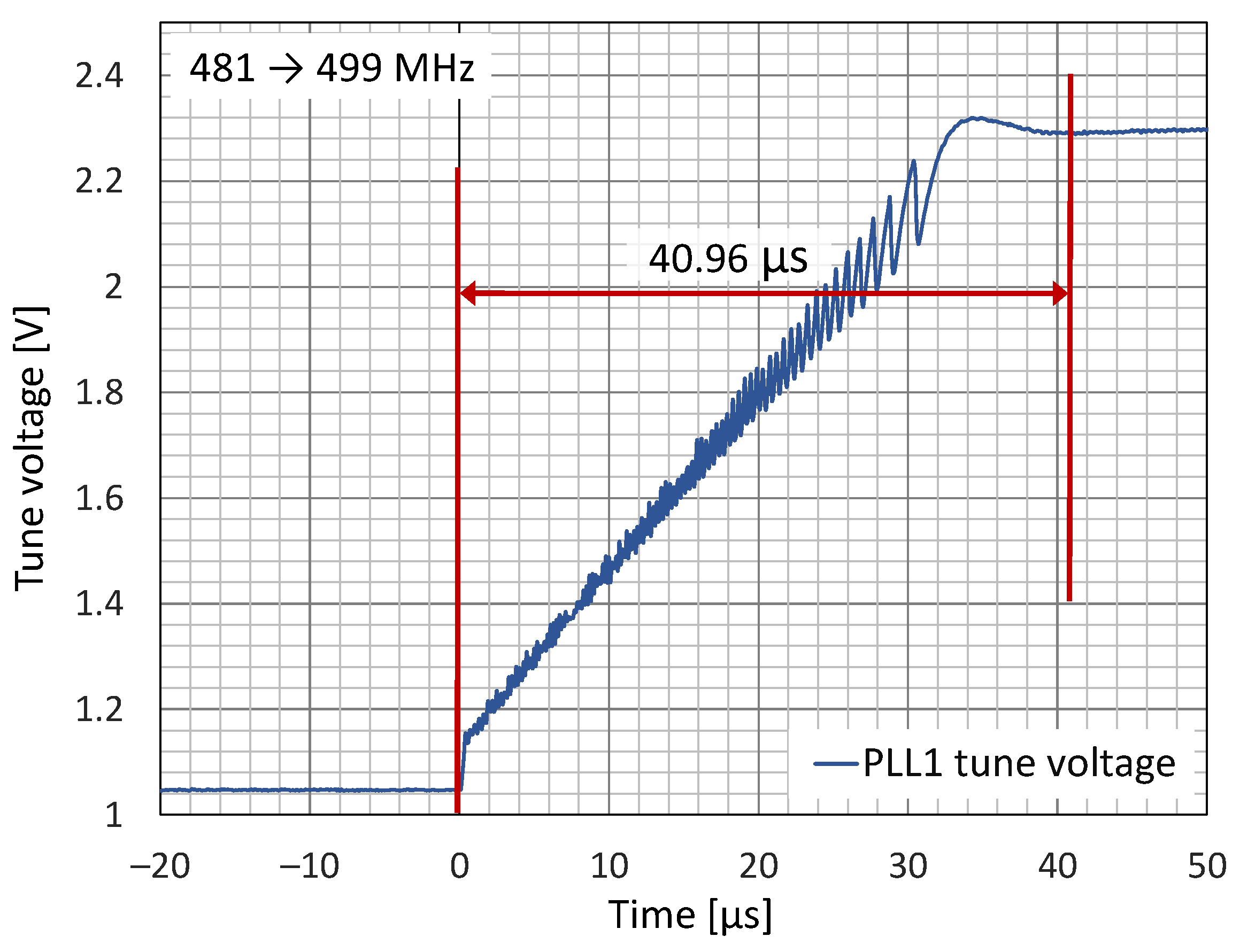
Figure 12 depicts the lock time of the PLL 1 oscillator. This measurement represents the worst-case scenario, where the frequency is swept from its minimum to its maximum value to perform a sufficient sweep at the output of PLL 2.
5. Discussion
The realization of a cascaded PLL design where the first stage performs the actual sweep and the second acts solely as a frequency multiplier became feasible only with recent advancements in integrated circuits incorporating PLL structures. A key limitation stemmed from the use of dual-modulus dividers (e.g., 16/17) for high-frequency division. While these dividers enable contiguous N values, they limit the minimum N achievable (in our case, to 16). To prevent fractional spurs, operation must occur away from integer multiples of the reference frequency. Consequently, the phase detector frequency needs to be approximately 20% higher than the desired sweep bandwidth. Because of the N divider limitation, this typically translates to operation above 300 MHz, a frequency that many traditional PLL ICs cannot handle as a reference input.
As demonstrated in Chapter 4, this approach achieves a fractional spur-free spectrum. However, a trade-off between phase noise and lock time remains, as with all PLLs. Some systems prioritize exceptional phase noise as they only change frequency during channel switching. Others require fast, wideband sweeps, thus necessitating minimal lock times. Spectrum analyzers, on the other hand, demand both qualities: fast sweep times for wider spans and good phase noise for narrowband measurements. In such cases, the otherwise excellent noise performance of the coaxial resonator comes at a cost. We observed that it tends to force the loop bandwidth to be narrower. A coil is a suitable choice in these scenarios, as the loop bandwidth can be more easily influenced by adjusting the charge pump current.
Our research also revealed that PLL 2 should have a loop bandwidth exceeding 10 kHz. Values below this significantly extend lock time for large frequency steps.
Sourcing coaxial resonators presents another challenge. While high-volume manufacturing is possible upon request, they are generally difficult to obtain otherwise. Siemens B69610-G5206 was ordered for the protype design [37].
For this research, 480 MHz was chosen as the first PLL frequency to demonstrate the working principle, as this was the readily available resonator frequency during the investigation. Ideally, this frequency should be closer to 800 MHz for our PLLs. Commercially available components could swiftly achieve 650 MHz without requiring special VCO construction. This option was also tested; however, despite changes in lock time performance, no significant improvement in phase noise was observed.
Table 1 summarizes the performance characteristics of various published wideband PLL synthesizer architectures. Our design demonstrates exceptional fractional spur performance and achieves a reasonable lock time. It is important to acknowledge the inherent challenges in directly comparing phase noise specifications due to the significant variations in operating frequency ranges across the published works. Generally, phase noise performance improves at lower frequencies. For transparency, we have included the worst-case scenario for phase noise reported in the reviewed literature within Table 1.
It is important to note that designs using published DDS techniques, like reference [34], may not achieve such a wide frequency range solely through the DDS implementation. These designs often employ additional multiplication, division, and filtering stages to cover the broader range. In the core of such designs, the DDS itself might operate within a narrower range, such as 0.305–1.1 GHz in reference [34]. Additionally, this reference does not directly report specific spur performance values, but rather their attenuation ratio.
6. Conclusions
This research demonstrates the feasibility of achieving wideband signal generation without the inherent complexity of DDS and dedicated DSP blocks, while preserving functional versatility. Furthermore, the proposed design offers the potential for integration onto a single silicon die, allowing both phase-locked loops to reside within a single compact package. Except for the first VCO coil, which may be challenging to integrate due to spatial constraints, and loop filters that necessitate high-value capacitors achievable only through alternative fabrication processes, most components could be implemented on-chip. This approach is a significant step towards a single-chip, wideband signal generator free from fractional-spur limitations. Such signals are crucial not only for next-generation mobile and satellite networks but also for fiber or wireless distribution systems [39,40]. In these systems, low-phase-noise local oscillator signals are essential for n-QAM wireless transmission, even when the microwave signals (or their lower-frequency references) are distributed optically [41]. This approach can be applied across GHz and potentially sub-THz carrier frequencies [42]. Regardless of the specific application, miniaturization and cost reduction will be key factors in ensuring future product competitiveness. This work paves the way for achieving these goals.
Author Contributions
Conceptualization, A.B.; methodology, A.B.; software, A.B.; validation, A.B.; investigation, A.B.; resources, A.B.; writing—original draft preparation, A.B.; writing—review and editing, B.B.; visualization, A.B.; supervision, B.B.; funding acquisition, B.B. All authors have read and agreed to the published version of the manuscript.
Funding
This research was funded by the Slovenian Research and Innovation Agency, grant numbers J2-3048 and J2-50072 and research core funding No. P2-0246.
Data Availability Statement
Schematic, production files, components list, and detailed measurements can be found at: https://github.com/aljazblatnik/Spectrum-analyzer/tree/main/LO1 (accessed on 2 May 2024).
Conflicts of Interest
The authors declare no conflicts of interest.
Appendix A
While the proposed design offers wideband operation, achieving a linear sweep presents a unique challenge. This section addresses this challenge and outlines the necessary considerations for sweep implementation.
Figure A1 illustrates the behavior observed when modifying the reference frequency (F) of PLL 1 while PLL 2 operates in integer-N mode. As the reference is swept, the entire output frequency range shifts proportionally. However, with each increment of the N value, the step size of this shift also increases. To maintain a constant frequency step size during N changes, the sweep needs to be segmented into smaller sections. Within each section, the reference fractional value (F) must be recalculated based on the current N value.
Figure A1.
Behavior of integer-N divider (N) in PLL 2 under varying reference frequency (F) in PLL 1.
Figure A1.
Behavior of integer-N divider (N) in PLL 2 under varying reference frequency (F) in PLL 1.

For the proposed design depicted in Figure 5, and for frequencies below 6 GHz (12 GHz with ×2 multiplication), the output frequency () can be calculated using Equation (A1).
From this equation, we can isolate N (integer divisor) and F (fractional part) as shown:
and
However, the chosen PLL 2 IC (STuW81300) has a specific requirement for the phase detector frequency. To generate outputs above 6 GHz (12 GHz), Equation (A1) is modified to the following:
N and F are then as follows:
and
This approach is only valid if the integrated oscillator banks cover at least ±80% of the frequency range spanned by the next and previous N values. In simpler terms, the oscillator banks must be able to perform the sweep within a single N value without requiring switching between banks. Unfortunately, not all commercially available ICs meet this requirement.
The influence of the printed circuit board on high-frequency circuits is crucial, as all such connections require a characteristic impedance of 50 Ω. While this is less critical for the PLL1 circuit due to its lower operating frequency and high-impedance reference clock input to PLL2, the high-frequency output of PLL2 presents a significant challenge. Maintaining a constant 50 Ω impedance across the wide bandwidth of 2–16 GHz is difficult to achieve in practice.
The prototype depicted in Figure A2 demonstrates optimized layout for an operational range of 8–12 GHz. Interestingly, during development, it was found that utilizing standard FR4 material offered a more practical solution compared to dedicated high-frequency laminates like the Rogers 4000 Series. Despite exhibiting higher losses due to its epoxy composition, FR4 effectively dampens potential higher-harmonic resonances.
Figure A2.
Photograph of manufactured prototypes (a) PLL1 and (b) PLL2.

A significant design consideration for high-frequency PCBs is the implementation of a multi-layer stack-up. Most manufacturers utilize thin prepregs (approximately 0.21 mm with a dielectric constant of 4.4) on the top and bottom layers. This allows for microstrip design with trace thicknesses of around 0.25 mm and a coplanar waveguide with ground plane on the first inner layer. This trace thickness aligns with the integrated circuit pad size, facilitating the implementation of impedance transformers. In our case, FR4 introduced only an additional 2 dB of loss at 10 GHz, while offering a substantial advantage in terms of reduced PCB manufacturing costs.
The complete reference circuit with all necessary design files is available in the GitHub repository linked in the Data Availability Statement section.
References
- Yang, S.-M.M. Modern Digital Radio Communication Signals and Systems; Springer Science+Business Media: New York, NY, USA, 2018; ISBN 978-3-319-71567-4. [Google Scholar]
- Alhashimi, H.F.; Hindia, M.N.; Dimyati, K.; Hanafi, E.B.; Safie, N.; Qamar, F.; Azrin, K.; Nguyen, Q.N. A Survey on Resource Management for 6G Heterogeneous Networks: Current Research, Future Trends, and Challenges. Electronics 2023, 12, 647. [Google Scholar] [CrossRef]
- Ho, C.-R.; Chen, M.S.-W. Smoothing the Way for Digital Phase-Locked Loops: Clock Generation in the Future with Digital Signal Processing for Mitigating Spur and Interference. IEEE Microw. 2019, 20, 80–97. [Google Scholar] [CrossRef]
- Jothimani, S.; Narmadha, A.; Santhiya, C.; Priya, S.S. Design of Various Modulation Schemes Using DDS. In Proceedings of the 2023 7th International Conference on Computing Methodologies and Communication (ICCMC), Erode, India, 23–25 February 2023; pp. 1–6. [Google Scholar]
- Matinmikko-Blue, M.; Yrjola, S.; Ahokangas, P. Spectrum Management in the 6G Era: The Role of Regulation and Spectrum Sharing. In Proceedings of the 2020 2nd 6G Wireless Summit (6G SUMMIT), Levi, Finland, 17–20 March 2020; pp. 1–5. [Google Scholar]
- Wang, Y.; Liu, Y.; Xu, H.; Li, Z.; Li, Z. A Wideband and Low Reference Spur PLL with Clock Feedthrough Suppressed and Low Current Mismatch Charge Pump and Symmetrical CML Divider. Electronics 2023, 12, 4164. [Google Scholar] [CrossRef]
- Jo, Y.; Kim, J.; Shin, Y.; Park, H.; Hwang, C.; Lim, Y.; Choi, J. A Wideband LO Generator for 5G FR1 Bands Using a Single LC -VCO-Based Subsampling PLL and a Ring-VCO-Based Fractional-Resolution Frequency Multiplier. IEEE J. Solid-State Circuits 2023, 58, 3338–3350. [Google Scholar] [CrossRef]
- Chen, J.; Kuylenstierna, D.; Gunnarsson, S.E.; He, Z.S.; Eriksson, T.; Swahn, T.; Zirath, H. Influence of White LO Noise on Wideband Communication. IEEE Trans. Microw. Theory Tech. 2018, 66, 3349–3359. [Google Scholar] [CrossRef]
- Goldberg, B.-G. Digital Frequency Synthesis Demystified; LLH Technology Publishing: Eagle Rock, VA, USA, 1999; ISBN 978-1-878707-47-5. [Google Scholar]
- Zhang, Y.; Tang, X.; Wei, Z.; Bao, K.; Jiang, N. A Ku-Band Fractional-N Frequency Synthesizer with Adaptive Loop Bandwidth Control. Electronics 2021, 10, 109. [Google Scholar] [CrossRef]
- Bulja, S.; Grebennikov, A. Variable Reflection-Type Attenuators Based on Varactor Diodes. IEEE Trans. Microw. Theory Tech. 2012, 60, 3719–3727. [Google Scholar] [CrossRef]
- Xu, D.; Zhang, Y.; Huang, H.; Sun, Z.; Liu, B.; Fadila, A.A.; Qiu, J.; Liu, Z.; Wang, W.; Xiong, Y.; et al. A 6.5-to-8 GHz Cascaded Dual-Fractional-N Digital PLL Achieving −63.7 dBc Fractional Spurs with 50 MHz Reference. In Proceedings of the 2023 IEEE Custom Integrated Circuits Conference (CICC), San Antonio, TX, USA, 23–26 April 2023; pp. 1–2. [Google Scholar]
- Shu, Z.; Lee, K.L.; Leung, B.H. A 2.4-GHz Ring-Oscillator-Based CMOS Frequency Synthesizer with a Fractional Divider Dual-PLL Architecture. IEEE J. Solid-State Circuits 2004, 39, 452–462. [Google Scholar] [CrossRef]
- Tsai, T.-H.; Sheen, R.-B.; Hsu, S.-Y.; Chang, Y.-T.; Chang, C.-H.; Staszewski, R.B. A Cascaded PLL (LC-PLL + RO-PLL) with a Programmable Double Realignment Achieving 204fs Integrated Jitter (100 kHz to 100 MHz) and −72 dB Reference Spur. In Proceedings of the 2022 IEEE International Solid-State Circuits Conference (ISSCC), San Francisco, CA, USA, 16–20 February 2022; pp. 1–3. [Google Scholar]
- Vishnu, R. A DDS-PLL Hybrid Based Fast Settling Wideband Frequency Synthesizer for Frequency Hopping Radios. Procedia Comput. Sci. 2017, 115, 748–755. [Google Scholar] [CrossRef]
- Bonfanti, A.; Amorosa, F.; Samori, C.; Lacaita, A.L. A DDS-Based PLL for 2.4-GHz Frequency Synthesis. IEEE Trans. Circuits Syst. II 2003, 50, 1007–1010. [Google Scholar] [CrossRef]
- Ishikawa, Y.; Ikeda, S.; Ito, H.; Kasamatsu, A.; Obara, T.; Noguchi, N.; Kamisuki, K.; Jiyang, Y.; Hara, S.; Ruibing, D.; et al. Design of High-Frequency Piezoelectric Resonator-Based Cascaded Fractional-N PLL with Sub-Ppb-Order Channel Adjusting Technique. In Proceedings of the 2017 22nd Asia and South Pacific Design Automation Conference (ASP-DAC), Chiba, Japan, 16–19 January 2017; pp. 43–44. [Google Scholar]
- Chary, P.P.; Shaik Peerla, R.; Dutta, A. A Simplified Gm−C Filter Technique for Reference Spur Reduction in Phase-Locked Loop. JLPEA 2024, 14, 17. [Google Scholar] [CrossRef]
- Biswas, D. Dual-Loop Integer PLL for Phase Noise Reduction. Analog Integr. Circuits Signal Process. 2022, 112, 537–544. [Google Scholar] [CrossRef]
- Vidmar, M. Extending Leeson’s Equation. Inf. MIDEM 2021, 51, 135–146. [Google Scholar] [CrossRef]
- Demir, A.; Mehrotra, A.; Roychowdhury, J. Phase Noise in Oscillators: A Unifying Theory and Numerical Methods for Characterization. IEEE Trans. Circuits Syst. I 2000, 47, 655–674. [Google Scholar] [CrossRef]
- Telba, A.A.; Qasim, S.M.; Noras, J.M.; Almashary, B.; El Ela, M.A. Behavioural Modelling and Simulation of Dual Cascaded PLL Based Frequency Synthesizer. In Proceedings of the 2007 14th International Conference on Mixed Design of Integrated Circuits and Systems, Ciechocinek, Poland, 21–23 June 2007; pp. 407–411. [Google Scholar]
- Boroditsky, R.; Gomez, J. Ultra Low Phase Noise 1 GHz OCXO. In Proceedings of the 2007 IEEE International Frequency Control Symposium Joint with the 21st European Frequency and Time Forum, Geneva, Switzerland, 29 May–1 June 2007; pp. 250–253. [Google Scholar]
- Brannon, A.; Breitbarth, J.; Popovic, Z. A Low-Power, Low Phase Noise Local Oscillator for Chip-Scale Atomic Clocks. In Proceedings of the IEEE MTT-S International Microwave Symposium Digest, Long Beach, CA, USA, 12–17 June 2005; pp. 1535–1538. [Google Scholar]
- Wersing, W. Microwave Ceramics for Resonators and Filters. Curr. Opin. Solid State Mater. Sci. 1996, 1, 715–731. [Google Scholar] [CrossRef]
- San-Blas, A.A.; Guglielmi, M.; Melgarejo, J.C.; Coves, A.; Boria, V.E. Design Procedure for Bandpass Filters Based on Integrated Coaxial and Rectangular Waveguide Resonators. IEEE Trans. Microw. Theory Tech. 2020, 68, 4390–4404. [Google Scholar] [CrossRef]
- Chen, Y.; Wu, K.-L. Metal-Dielectric Coaxial Dual-Mode Resonator for Compact Inline Bandpass Filters. In Proceedings of the 2023 IEEE/MTT-S International Microwave Symposium—IMS 2023, San Diego, CA, USA, 11–16 June 2023; pp. 403–405. [Google Scholar]
- Das, D.; Biswas, B.; Kumar, G.A.; Mondal, S. A Compact Very Narrow Band Coaxial Cavity Resonator Filter at X-Band with SMA Connector Feed. In Proceedings of the 2020 IEEE Calcutta Conference (CALCON), Kolkata, India, 28–29 February 2020; pp. 93–96. [Google Scholar]
- Fiedziuszko, S.J.; Holmes, S. Dielectric Resonators Raise Your High-Q. IEEE Microw. 2001, 2, 50–60. [Google Scholar] [CrossRef]
- Manjunatha, R.H.V.; Manjunath, R.K. Design and Simulation of Ku-Band Voltage Tuned Dielectric Resonator Oscillator. In Proceedings of the 2018 International Conference on Communication and Signal Processing (ICCSP), Chennai, India, 3–5 April 2018; pp. 0299–0304. [Google Scholar]
- Skyworks. Coaxial Resonators for Voltage-Controlled Oscillator (VCO) Applications 2013. Available online: http://www.edatop.com/down/faq/hfss/Coaxial_Resonators_for_VCOs_202664A.pdf (accessed on 23 March 2024).
- Rohde, U.; Poddar, A. Novel Multi-Coupled Line Resonators Replace Traditional Ceramic Resonators in Oscillators/VCOs. In Proceedings of the 2006 IEEE International Frequency Control Symposium and Exposition, Miami, FL, USA, 4–7 June 2006; pp. 432–442. [Google Scholar]
- Hitch, B.; Holden, T. Phase Locked DRO/CRO for Space Use. In Proceedings of the International Frequency Control Symposium, Orlando, FL, USA, 28–30 May 1997; pp. 1015–1023. [Google Scholar]
- Jeon, Y. Study of Ultra-Broadband Synthesizer of Fast Indirect Type in a 0.5–18 GHz Range for SIGINT System. Electronics 2023, 13, 48. [Google Scholar] [CrossRef]
- Mincong, C.; Ruiyu, L.; Tao, H. Study of Optimized Design of DDS Based on FPGA. In Proceedings of the 2019 14th IEEE International Conference on Electronic Measurement & Instruments (ICEMI), Changsha, China, 1–3 November 2019; pp. 150–154. [Google Scholar]
- Nilsson, P.; Gerrits, J.F.M.; Yuan, J. A Low Complexity DDS IC for FM-UWB Applications. In Proceedings of the 2007 16th IST Mobile and Wireless Communications Summit, Budapest, Hungary, 1–5 July 2007; pp. 1–5. [Google Scholar]
- Siemens Matsushita. Coaxial Ceramic Resonators. Available online: https://www.rf-microwave.com/resources/products_attachments/5a4386ce05742.pdf (accessed on 4 April 2024).
- Zhang, X.; Du, Q.; Liu, C.; Zhang, H.; Ma, Y.; Li, Y.; Li, J. A Low Phase Noise Frequency Synthesizer with a Fourth-Order RLC Loop Filter. Electronics 2023, 12, 224. [Google Scholar] [CrossRef]
- Hilt, A. Availability and Fade Margin Calculations for 5G Microwave and Millimeter-Wave Anyhaul Links. Appl. Sci. 2019, 9, 5240. [Google Scholar] [CrossRef]
- Ilgaz, M.A.; Lavric, A.; Batagelj, B. Phase-Noise Degradation of an Optically Distributed Local Oscillator in a Radio Access Network. Radioengineering 2021, 30, 10–15. [Google Scholar] [CrossRef]
- Hilt, A.; Zolomy, A.; Berceli, T.; Jaro, G.; Udvary, E. Millimeter Wave Synthesizer Locked to An Optically Transmitted Reference Using Harmonic Mixing. In Proceedings of the International Topical Meeting on Microwave Photonics, Duisburg, Germany, 3–5 September 1997; pp. 91–94. [Google Scholar]
- Krause, B.; Lavric, A.; Tebart, J.; Stohr, A.; Preu, S. Phase Noise of an Electro-Optic Terahertz Comb. Opt. Express 2024. [Google Scholar] [CrossRef]
Figure 1.
PLL structure.

Figure 2.
Contributions of various noise sources within the phase-locked loop (PLL) to the overall phase noise performance. Note that the noise contributions are presented on separate graphs and are not drawn to the same scale for better visualization of each source’s relative impact.
Figure 2.
Contributions of various noise sources within the phase-locked loop (PLL) to the overall phase noise performance. Note that the noise contributions are presented on separate graphs and are not drawn to the same scale for better visualization of each source’s relative impact.

Figure 3.
Phase noise shaping. Simulation of phase noise contributions at (a) 43 kHz and (b) 103 kHz loop bandwidth. The figure illustrates the contributions of building blocks within a functional loop, rather just individual unlocked pieces.
Figure 3.
Phase noise shaping. Simulation of phase noise contributions at (a) 43 kHz and (b) 103 kHz loop bandwidth. The figure illustrates the contributions of building blocks within a functional loop, rather just individual unlocked pieces.

Figure 4.
Proposed broadband oscillator structure: cascaded connection of two phase-locked loops.

Figure 5.
Specific frequencies and PLL integrated circuits employed in the fabricated prototype.

Figure 6.
Limitations of building blocks for selected integrated circuits in a functioning prototype.
Figure 6.
Limitations of building blocks for selected integrated circuits in a functioning prototype.

Figure 7.
Photograph of the PLL 1 prototype. The coaxial resonator is clearly visible in the lower right corner. This image demonstrates the simplicity of the proposed frequency sweep topology. Implemented on a single-layer PCB without vias, this design is well-suited for rapid prototyping. Notably, this approach translates to a cost-effective solution for industrial applications.

Figure 8.
This photograph shows the experimental setup for the measurements. The computer controls the equipment via GP-IB and USB interfaces. A block diagram detailing the connections is presented in the upper right corner for additional clarity.
Figure 8.
This photograph shows the experimental setup for the measurements. The computer controls the equipment via GP-IB and USB interfaces. A block diagram detailing the connections is presented in the upper right corner for additional clarity.

Figure 9.
Phase noise characteristics of the PLL 1 reference oscillator: (a) the impact of a ceramic coaxial resonator (red curve) versus a standard wire coil (blue curve) within the VCO circuit and (b) the effect of the coaxial resonator (red curve) narrowing the otherwise wideband loop filter (blue curve).
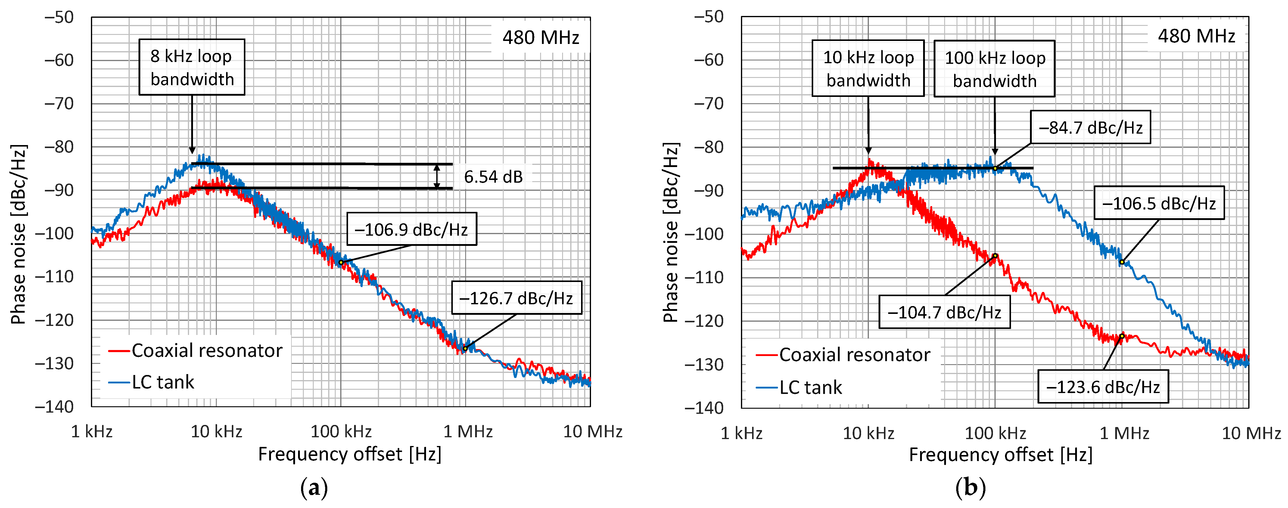
Figure 10.
Measured phase noise at the output of PLL 2 (STuW81300) for (a) 5 GHz and (b) 10 GHz. The curves illustrate the impact of different VCO components within PLL 1 on the overall phase noise. The solid blue and red curves represent the phase noise with a standard inductor and a ceramic coaxial resonator, respectively, used in the VCO circuit of PLL 1. The black curve depicts the phase noise behavior when the loop bandwidth of PLL 2 is reduced by adjusting the charge pump current.

Figure 11.
Spectrum of the output signal (PLL 2) when the reference signal (PLL 1) is set to its least favorable fractional division ratio. This operating condition is chosen to illustrate the maximum level of fractional spurs that may be encountered. In order to improve signal averaging and enhance the visibility of spurs, the resolution bandwidth (RBW) was set to 10 kHz, while the video bandwidth (VBW) was set to 100 Hz.
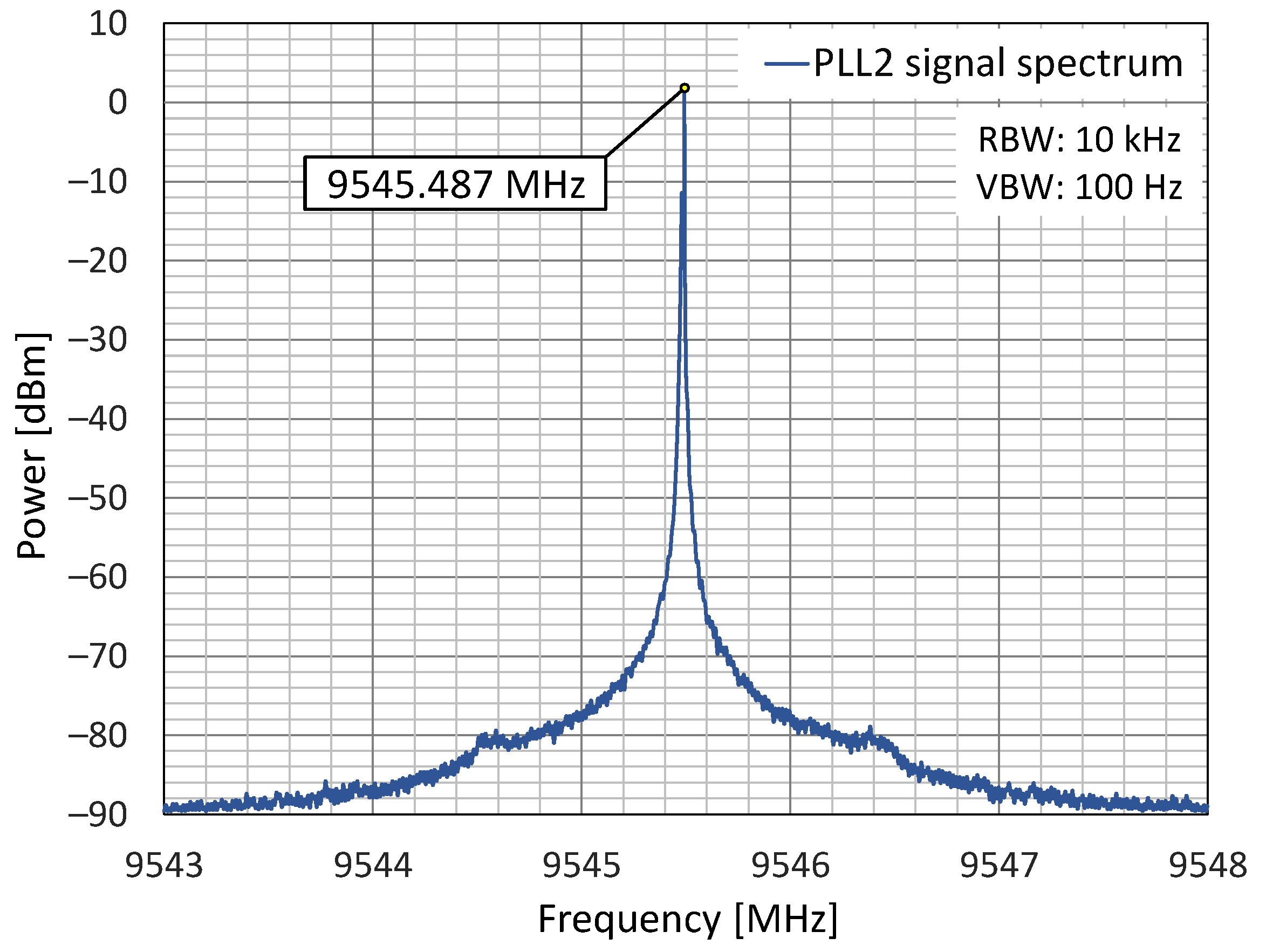
Figure 12.
The lock-in time required for the PLL 1 oscillator when its frequency is swept between 481 MHz and 499 MHz.
Figure 12.
The lock-in time required for the PLL 1 oscillator when its frequency is swept between 481 MHz and 499 MHz.

Table 1.
Comparative analysis of performance with other similar designs previously published.
| Reference | This Work | [15] | [16] | [10] | [38] | [34] |
|---|---|---|---|---|---|---|
| Architecture | PLL-PLL | DDS-PLL | DDS-PLL | Frac PLL | Frac PLL | DDS |
| Frequency Range [GHz] | 1.925–16 | 0.13–1.75 | 2.36–2.44 | 11.37–14.8 | 1.426 | 0.5–18 |
| Phase Noise 1 [dBc/Hz] | −121 @ 1 M −102.5 @ 100 k | −134 @ 1 M −103 @ 100 k | −99 @ 1 M −94 @ 100 k | −112.5 @ 1 M −79 @ 100 k | −138.4 @ 1 M −113.9 @ 100 k | −110.9@ 1 M −112.9 @ 100 k |
| Fractional Spurs 1 [dBc] | −80 | −75 | −53 | N/D | −69 | >−60 |
| Lock Time 1 [µS] | 41 | 51 | 1 | 24 | 94 | N/A |
1 Worst case scenario published.
Disclaimer/Publisher’s Note: The statements, opinions and data contained in all publications are solely those of the individual author(s) and contributor(s) and not of MDPI and/or the editor(s). MDPI and/or the editor(s) disclaim responsibility for any injury to people or property resulting from any ideas, methods, instructions or products referred to in the content. |
© 2024 by the authors. Licensee MDPI, Basel, Switzerland. This article is an open access article distributed under the terms and conditions of the Creative Commons Attribution (CC BY) license (https://creativecommons.org/licenses/by/4.0/).
Share and Cite
MDPI and ACS Style
Blatnik, A.; Batagelj, B. Wideband Low Phase-Noise Signal Generation Using Coaxial Resonator in Cascaded Phase Locked Loop. Electronics 2024, 13, 1934. https://doi.org/10.3390/electronics13101934
AMA Style
Blatnik A, Batagelj B. Wideband Low Phase-Noise Signal Generation Using Coaxial Resonator in Cascaded Phase Locked Loop. Electronics. 2024; 13(10):1934. https://doi.org/10.3390/electronics13101934
Chicago/Turabian StyleBlatnik, Aljaž, and Boštjan Batagelj. 2024. "Wideband Low Phase-Noise Signal Generation Using Coaxial Resonator in Cascaded Phase Locked Loop" Electronics 13, no. 10: 1934. https://doi.org/10.3390/electronics13101934
Note that from the first issue of 2016, this journal uses article numbers instead of page numbers. See further details here.