Article

Disturbance Rejection Control of Grid-Forming Inverter for Line Impedance Parameter Perturbation in Weak Power Grid

by
Mayue Huang
and
Hui Li
*
College of Automation Engineering, Shanghai University of Electric Power, Shanghai 200090, China
*
Author to whom correspondence should be addressed.
Electronics 2024, 13(10), 1926; https://doi.org/10.3390/electronics13101926
Submission received: 22 April 2024 / Revised: 9 May 2024 / Accepted: 13 May 2024 / Published: 14 May 2024
(This article belongs to the Special Issue Applications, Control and Design of Power Electronics Converters)

Abstract

:
When a grid-forming (GFM) inverter is connected to a low- or medium-voltage weak power grid, the line impedance with resistive and inductive characteristics will cause power coupling. Typical GFM decoupling control strategies are designed under nominal line impedance parameters. However, there are deviations between the nominal line impedance and actual parameters, resulting in poor decoupling effects. Aiming at this problem, this paper proposes a power decoupling strategy based on a reduced-order extended state observer (RESO). Firstly, the power dynamic model of the GFM is established based on the dynamic phasor method. Then, the model deviation and power coupling due to line impedance parameter perturbation are estimated as internal disturbances of the system, and the disturbances are compensated on the basis of typical power control strategy and virtual impedance decoupling. Good decoupling performance is obtained under different impedance parameters, improving the control strategy’s robustness. Finally, the effectiveness of the proposed method is verified by the results of RT Box hardware-in-the-loop experiments.

1. Introduction

Conventional fossil energy sources are connected to the grid through Synchronous Generators (SGs), and the presence of a large number of SGs slows down the dynamics of the entire system [1]. With a large number of new energy sources connected to the power system, the proportion of inverter-based resources (IBRs) power generation in the grid has been increasing, replacing most of the SGs and becoming an important trend in the development of the power system [2]. Conventional grid-following (GFL) inverters are synchronized with the grid through the phase-locked loop (PLL), and their proper operation relies on the presence of a voltage source in the system which can build a voltage reference. However, more IBRs also lead to faster system dynamics, and the stable operation of the GFL will be affected, resulting in a lack of voltage support and inertial responsiveness of the grid [3,4].
As a new solution, GFM inverters have been proposed and widely and deeply researched [5,6,7,8]. By simulating the characteristics of a synchronous generator, a GFM applies the rotor motion equations of the synchronous generator and the primary frequency modulation to the control of the inverter [9] so that the external characteristics of the inverter present the inertia and damping characteristics similar to those of the synchronous generator [10]. The system voltage and frequency can be established independently [11,12], thus effectively improving the stability of the power system [13]. In the GFMs above, it is assumed that the impedance of the line is purely inductive, and this assumption is consistent with the case of high-voltage grids. After connecting to the low- and medium-voltage weak grid, the line impedance ratio R/X is relatively large, so there is a significant coupling between active power and reactive power [14].
Power modeling is the basis of theoretical analysis. There are mainly steady-state models and dynamic models. In [15,16,17], the steady-state models of active and reactive power were established to analyze the GFM’s stability and to design power control parameters, respectively. The transfer function of the steady-state model is constant and cannot reflect the dynamic characteristics of the line impedance. The dynamic models of active and reactive power are developed in [18,19]. Due to the low bandwidth of the power control loop, the analysis with the steady-state model also yields results consistent with those analyzed with the dynamic model. However, the power coupling involves transient processes, and it is more appropriate to use the dynamic model. This paper uses the dynamic phasor method [20] to develop a dynamic model that can more accurately describe system behavior during the unsteady state or transient processes.
In order to solve the power coupling problem, many scholars have conducted a series of research studies. In [21,22,23], the virtual power method is used for power decoupling. Based on the impedance angle of the line impedance, the active and reactive power coordinates are transformed into virtual active and reactive power, which are controlled by frequency and voltage magnitude, respectively. However, implementing this method is subject to the accurate acquisition of the resistance–inductance ratio in the line. In [24,25], voltage and frequency cross-channel feedforward compensation methods are proposed for droop control and the virtual synchronous generator (VSG), respectively. In [26], a reactive power feedforward compensation method is proposed to reduce power coupling. Similar problems exist with the virtual power method, as feedforward decoupling requires knowledge of the exact line impedance parameters and the power angle of the GFM. The most common power decoupling method is through the reconstruction of the inverter output impedance by the virtual impedance method [27,28]. In [29], a strategy to introduce virtual inductance in the control system was proposed based on increasing the neutral inductive component of the line impedance, which effectively reduces the power coupling between active power P and reactive power Q. However, it is pointed out in [30] that the power decoupling capability is somewhat constrained due to the inherent d-axis voltage drop caused by the virtual inductor. A virtual negative resistance approach was introduced in [31] that reduces the resistive characteristics of the line impedance. As a result, the line impedance is inductive, and the power coupling between P and Q is reduced.
An easily overlooked issue in existing studies is that the variation of line impedance is not considered. If a parameter perturbation in the line impedance causes it to deviate from the nominal value, the power decoupling performance worsens. In [32], a total sliding-mode controller (TSMC) is used for power decoupling, and excellent decoupling performance can be obtained when the line impedance varies in a small range. However, the jitter phenomenon restricts the robustness of the power decoupling, and the stronger the robustness, the worse the jitter phenomenon. In [33], a feedforward neural network (FNN) framework is used to simulate the TSMC law for robust and accurate decoupling control. The simulation and experimental results verify the robustness of power decoupling, but the design of the control system is complex and cannot be implemented on a microcontroller. In [34], a power decoupling strategy based on an extended state observer is proposed. On the basis of the feedforward decoupling method, the power coupling is estimated as an internal disturbance of the system using an extended state observer (ESO), and the output of the feedforward decoupling method is compensated to improve the robustness of the feedforward decoupling method. Feedforward decoupling can make the strongly coupled channel paired and the weakly coupled channel decoupled. However, when the resistive component of the line impedance is larger than the inductive component, the P-δ and Q-E control channels are weakly coupled, which does not satisfy the principle of optimal pairing of the control channels.
Therefore, this paper proposes a power decoupling strategy based on a RESO. The factors affecting the power control performance, such as model deviation and power coupling caused by line impedance parameter perturbation, are considered internal disturbances. These disturbances are observed in real time by a RESO, and the disturbance compensation is performed based on the virtual impedance decoupling method. Good decoupling performance is obtained even under different impedance parameters, and the robustness of virtual impedance decoupling is improved. The main contributions of this paper are as follows:
  • A small-signal model of the power dynamics of the GFM is established based on the dynamic phasor method, and according to the small-signal model, the disturbances existing in the power control of the GFM after considering the line impedance parameter perturbation are analyzed.
  • A power decoupling strategy based on RESO is proposed. The RESO reduces the amount of control system arithmetic and the system’s phase delay. Good decoupling performance can be obtained even under different impedance parameters, and the robustness of the virtual impedance decoupling method is improved.
  • The transfer functions of the disturbance estimation capability and disturbance estimation error of two ESOs are derived, and the disturbance estimation capability of RESO under different observation bandwidths are analyzed.
The organizational structure of this paper is as follows: Section 2 introduces typical control strategies for GFM inverters and analyzes the disturbance after considering the line impedance parameter perturbation; Section 3 proposes the design of a power decoupling control strategy based on a RESO and analyzes the performance of ESO disturbance estimation; Section 4 illustrates the hardware-in-the-loop experimental results; and Section 5 provides the conclusion.

2. Typical Control and Disturbance Analyses of GFM Inverters

2.1. Typical Control Strategies for GFM Inverters

The main circuit topology and control block diagram of the GFM inverter are shown in Figure 1. The DC source is connected to the AC grid using a three-phase voltage source inverter, and the system as a whole consists of a DC-side equivalent power supply, an inverter bridge, an LCL-type filter, an equivalent line impedance, and a grid configuration. Among them, L1 is the inverter-side inductance; C is the filter capacitance; L2 is the grid-side inductance; Rg and Lg are the equivalent line resistance and inductance between the GFM and the grid; udc is the DC bus voltage, ux is the inverter bridge arm voltage, i1x is the inverter-side inductance current, u2x is the inverter output voltage, i2x is the inverter output current, and ugx is the grid voltage (x = a, b, c); E is the virtual internal potential of the VSG; and δ is the virtual rotor angle, generated by the virtual angular frequency ω.
In the power control of the GFM inverter, the power control link of the virtual synchronous machine plays a crucial role. It consists of two main parts, active and reactive power control, as shown in Figure 1. The active power control link is realized by simulating the real rotor’s equations of motion and the prime mover’s speed-governing equations, using P-ω for control. The specific expression is shown in Equation (1).
P ref ω 0 P ω 0 D p ( ω ω 0 ) = J p d ω d t
where Jp and Dp are the active virtual inertia and droop coefficient of the VSG, respectively; Pref and P are the active power setpoint and the actual active power output from the inverter, respectively; ω0 and ω are the rated and actual output angular frequency of the VSG, respectively.
The reactive power control link adopts Q-E control by simulating the voltage regulation characteristics of the synchronous generator, thus generating the magnitude of the virtual internal potential, with the specific expression shown in Equation (2).
Q ref Q + D q ( E 0 E ) = J q d E d t
where Jq and Dq are the virtual inertia coefficient and droop coefficient of VSG reactive power, respectively; Qref and Q are the set value of reactive power and the actual output reactive power, respectively; and E0 is the peak value of the rated output voltage of VSG.
Considering that the virtual steady-state synchronous complex impedance control can significantly reduce the output impedance of the GFM in the high-frequency range, which further improves the stability of the system, the power decoupling control is carried out based on the virtual steady-state synchronous complex impedance. The mathematical expression of the virtual impedance control link in the dq coordinate system is given by the following:
u 2 dref = E R v i 2 d + X v i 2 q u 2 qref = 0 R v i 2 q X v i 2 d
where Rv and Xv are the virtual resistance and virtual reactance of the GFM, respectively, Xv = ω0·Lv, and Lv is the virtual inductance.
The voltage–current control is controlled by inner-loop inductor current P control and outer-loop output voltage PI control. After the compensation of the virtual impedance link, the voltage reference value is fed into the voltage–current double closed loop to achieve the fast-tracking of the GFM output voltage. Finally, the modulating waves eod and eoq are fed into the space vector pulse width modulation (SVPWM) link for modulation to drive the inverter bridge.

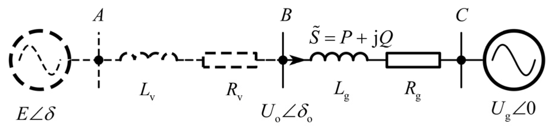
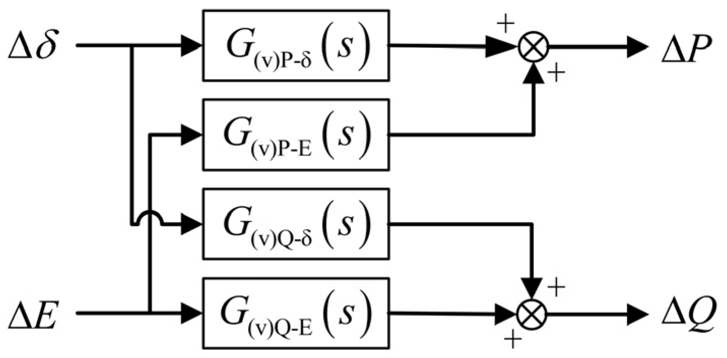
2.2. Disturbance Analysis after Considering Line Impedance Parameter Perturbation

In order to ensure a suitable voltage-following capability for output voltage control, the bandwidth of the voltage–current dual-loop closure is set to be much larger than that of the external power control loop. As a result, the VSG-controlled GFM can be simplified as a controllable voltage source [27]. After introducing the virtual impedance control, the equivalent circuit diagram of its access to the AC grid is shown in Figure 2. Where E is the virtual internal potential amplitude of the VSG; δ is the phase difference between the virtual internal potential of the VSG and the grid voltage, which is the power angle; Uo and δo are the voltage amplitude at the output of the GFM and the phase difference between the GFM output and the grid voltage, respectively, after virtual impedance compensation is performed; and S ˜ , P, and Q are the actual complex power, active power, and reactive power output from the virtual synchronous machine, respectively.
Conventional phase quantities are built on the assumption that the power electronic system is a quasi-steady state, which presupposes that the rate of change in the amplitude and phase of the system voltages, currents, and other physical quantities is much less than the system’s base frequency angular velocity ω0. In a quasi-steady state, the amplitude within the frequency bandwidth (−ω0, ω0) is considered to be constant. Therefore, the electrical quantities can be approximated as a sinusoidal waveform, which can be expressed in terms of the phase quantity method. However, in the dynamic phase volume concept, the phase volume change rate is close to the angular velocity of the fundamental frequency, although it is still less than that. At the same time, its frequency bandwidth is also close to, but less than, the fundamental frequency, and within this bandwidth, the amplitude is no longer constant but varies over a range. Thus, the dynamic phase can more accurately describe the system’s behavior during unsteady or transient processes.
For inductive elements, the dynamic phase model [20] is
U ˙ L = L d I ˙ L d t + j ω 0 L I ˙ L
where U ˙ L is denoted as the dynamic phase form of the variable uL, which is the inductive voltage; I ˙ L is denoted as the dynamic phase form of the variable iL, which is the inductive current. When building the quasi-static model, it will be ignored that the differential terms of the dynamic phasors on the right side of the equal sign with respect to time are often neglected.
According to Figure 2 combined with Equation (4), the relationship between the GFM output voltage and output current I can be obtained as follows:
E ˙ U ˙ o = ( R ν + j X ν ) I ˙ U ˙ o U ˙ g = ( R g + j X g ) I ˙ + L g d I ˙ d t
Since the virtual impedance method is designed by steady-state synchronous impedance control, the differential term is not considered in the virtual impedance modeling.
Laplace transformation of Equation (5) and collation gives the current flowing into the grid as
I ˙ = E δ U o δ o R v + j X v = U o δ o U g 0 R g + j X g + s L g = E δ U g 0 R + j X + s L g
where R = Rv + Rg and X = Xv + Xg. Then, the inverter output complex power can be found as follows:
S ˜ = 3 U ˙ o · I ˙ * = P + j Q = 3 E δ I ˙ R v + j ω L v · I ˙ * = 3 E δ I ˙ * I ˙ I ˙ * R v + j ω L v
The actual output active power P and reactive power Q of the GFM considering the dynamic process can be obtained as follows:
P = 3 R v ( E U g cos δ U g 2 ) + ( R g + s L g ) ( E 2 E U g cos δ ) + X E U g sin δ ( R + s L g ) 2 + X 2 Q = 3 X v ( E U g cos δ U g 2 ) + X g ( E 2 E U g cos δ ) ( R + s L g ) E U g sin δ ( R + s L g ) 2 + X 2
The output power expression of the grid-forming inverter is linearized and small-signal modelled at (δ0, E0). The partial derivatives are obtained for P and Q respectively:
Δ P Δ Q = P δ P E Q δ Q E ( δ 0 , E 0 ) Δ δ Δ E = G v Δ δ Δ E
where
G v s = G v P - δ ( s ) G v P - E ( s ) G v Q - δ ( s ) G v Q - E ( s ) = k 11 s + k 12 g 1 s 2 + g 2 s + g 3 k 21 s + k 22 g 1 s 2 + g 2 s + g 3 k 31 s + k 32 g 1 s 2 + g 2 s + g 3 k 41 s + k 42 g 1 s 2 + g 2 s + g 3
where the individual numerator denominator coefficients of the transfer function are as follows:
g 1 = L g 2 g 2 = 2 L g R g 3 = R 2 + X 2 k 11 = E 0 U g sin δ 0 L g k 12 = E 0 U g cos δ 0 X + sin δ 0 R g R v k 21 = 2 E 0 U g cos δ 0 L g k 22 = U g cos δ 0 R v R g + 2 E 0 R g + U g sin δ 0 X k 31 = E 0 U g cos δ 0 L g k 32 = E 0 U g sin δ 0 X g X v cos δ 0 R k 41 = U g sin δ 0 L g k 42 = U g cos δ 0 X v X g + 2 E 0 X g U g sin δ 0 R
From Equation (11), the power dynamic small-signal model of GFM is shown in Figure 3.
Rewriting the small-signal model in the time–domain progression can be performed as follows:
Δ P ¨ + g 2 g 1 Δ P ˙ + g 3 g 1 Δ P = k 12 g 1 Δ δ + k 11 g 1 Δ δ ˙ + k 21 g 1 Δ E ˙ + k 22 g 1 Δ E Δ Q ¨ + g 2 g 1 Δ Q ˙ + g 3 g 1 Δ Q = k 42 g 1 Δ E + k 41 g 1 Δ E ˙ + k 31 g 1 Δ δ ˙ + k 32 g 1 Δ δ
In actual working conditions, there is a parameter perturbation in the line impedance. Not only is there an accuracy error between the actual and nominal parameters of the components, but also, if the grid is affected by factors such as environment, electromagnetic interference, mechanical stress changes, etc., the line impedance parameters also deviate from the nominal value, and the effect of power decoupling will become worse. Therefore, the system can be separated according to Equation (13) as follows:
Δ P ¨ + g 2 n g 1 n Δ P ˙ + g 3 n g 1 n Δ P = g 2 n g 1 n g 2 g 1 Δ P ˙ + g 3 n g 1 n g 3 g 1 Δ P + k 12 n g 1 n Δ δ + k 12 n g 1 n k 12 g 1 Δ δ + k 11 g 1 Δ δ ˙ + k 21 g 1 Δ E ˙ + k 22 g 1 Δ E Δ Q ¨ + g 2 n g 1 n Δ Q ˙ + g 3 n g 1 n Δ Q = g 2 n g 1 n g 2 g 1 Δ Q ˙ + g 3 n g 1 n g 3 g 1 Δ Q + k 42 n g 1 n Δ E + k 42 n g 1 n k 42 g 1 Δ E + k 31 g 1 Δ δ ˙ + k 32 g 1 Δ δ + k 41 g 1 Δ E ˙
where the coefficients with the label n indicate the use of nominal line impedance parameters, and the coefficients without the label n indicate the use of actual line impedance parameters. As the control structure between active and reactive power is similar, the active power control loop is analyzed as an example. Let
f p = g 2 n g 1 n g 2 g 1 Δ P ˙ + g 3 n g 1 n g 3 g 1 Δ P + k 12 n g 1 n k 12 g 1 Δ δ + k 11 g 1 Δ δ ˙ + k 21 g 1 Δ E ˙ + k 22 g 1 Δ E f = g 2 n g 1 n Δ P ˙ g 3 n g 1 n Δ P + f p
where f is the total disturbance and fp is the disturbance without model information. The total disturbance f has several components, including k 22 g 1 Δ E and k 21 g 1 Δ E ˙ , which are the disturbances coupled between active and reactive power after being compensated by virtual impedance; g 2 n g 1 n g 2 g 1 Δ P ˙ , g 3 n g 1 n g 3 g 1 Δ P and k 12 n g 1 n k 12 g 1 Δ δ are the disturbances due to model deviation; g 2 n g 1 n Δ P ˙ and g 3 n g 1 n Δ P are the model information of the system, which is a part of the model different from the integral series-type standard type, and are estimated together in the estimation of the total disturbances. However, when power decoupling is performed, in order to not change the model of the original system, only the disturbances fp are compensated which does not contain the model information.

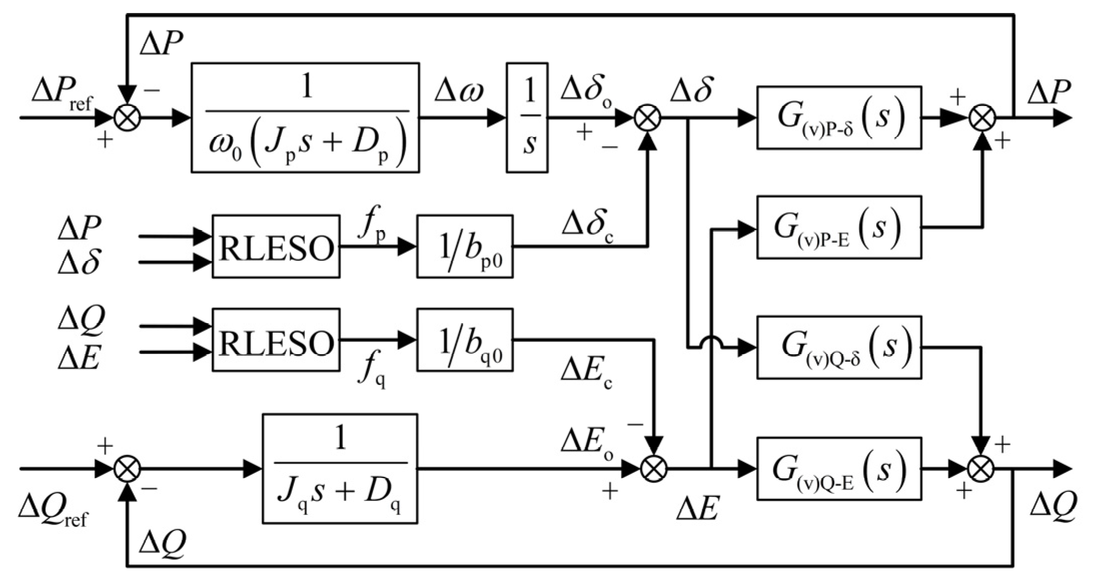
3. Decoupling Control Strategy of GFM Inverter Based on RESO

3.1. Design of RESO

Design the controller as an example of an active power control loop such that
y = Δ P , u = Δ δ , b p 0 = k 12 n g 1 n , a 1 = g 3 n g 1 n , a 2 = g 2 n g 1 n
The state variables are selected as follows:
x 1 = y = Δ P x 2 = y ˙ = Δ P ˙ x 3 = f = a 1 x 1 a 2 x 2 + f p h = f ˙
The expansion equation of state for the GFM active power can be obtained as follows:
x ˙ 1 x ˙ 2 x ˙ 3 = 0 1 0 0 0 1 0 0 0 x 1 x 2 x 3 + 0 0 b p 0 0 0 1 u h y = x 1
It can be seen through Equation (14) that the system is a second-order system and requires the design of a third-order ESO to estimate the total disturbance f. The state equation is
z ˙ 1 = z 2 + β 1 x 1 z 1 z ˙ 2 = z 3 + b p 0 u + β 2 x 1 z 1 z ˙ 3 = β 3 x 1 z 1
where z1, z2, and z3 are the real-time observations of the state variables x1, x2, and x3, respectively, and β1, β2, and β3 are the observer gains.
The performance of the ESO-based controller mainly depends on the accuracy of the state and disturbance estimation [35]. The higher the order of the ESO, the more obvious the hysteresis effect of the observed disturbances is [36], which affects the effectiveness of the compensation of the disturbance fp. Since the output voltage and current of the GFM inverter can be obtained through sensors and the output power of the inverter is calculated, the structure of ESO, by observing the output power, can be deleted, and a RESO can be used to reduce the complexity of the algorithm. Equation (17) can be transformed into
x ˙ 2 x ˙ 3 = 0 1 0 0 x 2 x 3 + b p 0 0 0 1 u h y = x 2
RESO can be designed to:
z ˙ 2 = z 3 + b p 0 u + l 2 x 2 z 2 z ˙ 3 = l 3 x 2 z 2
where l2 and l3 are the reduced-order observer gains. RESO requires the differentiation of ΔP, which introduces high-frequency noise into the control loop and adversely affects the control effectiveness. Therefore, the RESO must be reconstructed to avoid differential operations. This can be obtained by moving the term containing x2 in Equation (19) to the left side of the equation:
z ˙ 2 l 2 x ˙ 1 = z 3 + b p 0 u l 2 z 2 z ˙ 3 l 3 x ˙ 1 = l 3 z 2
The new state variable is introduced such that
z ¯ 2 = z 2 l 2 x 1 z ¯ 3 = z 3 l 3 x 1
According to Equations (21) and (22), the state equation can be obtained as follows:
z ¯ ˙ 2 = z ¯ 3 + l 3 x 1 + b p 0 u l 2 z ¯ 2 + l 2 x 1 z ¯ ˙ 3 = l 3 z ¯ 2 + l 2 x 1
According to the pole configuration method, the poles of the observer are configured to −ωo, which gives an observer gain of
l 2 = 2 ω o , l 3 = ω o 2
If the reconfigured RESO can observe z ¯ 2 , z ¯ 3 correctly, then z1 and z2 can be inversely found according to Equation (22), and fp can be found according to Equation (16). The simplified control block diagram of the GFM power decoupling based on RESO is shown in Figure 4. The compensation amount of decoupling is designed as follows:
Δ δ c = f p / b p 0 Δ E c = f q / b q 0
As an example, the active power control loop is obtained by bringing Equation (25) into Equation (13) in conjunction with Figure 4:
Δ P ¨ + a 2 Δ P ˙ + a 1 Δ P = b p 0 Δ δ + f p = b p 0 Δ δ o Δ δ c + f p = b p 0 Δ δ o f p / b p 0 + f p = b p 0 Δ δ o
The model deviation due to line impedance parameter perturbation and the disturbance fp of power coupling are accurately estimated by RESO, and the disturbance compensation strategy is implemented based on typical power control strategy and virtual impedance decoupling. When the deviation of the actual line impedance parameters occurs, the power coupling can be suppressed, and the independent control of active and reactive power can be realized.

3.2. Frequency Domain Analysis of ESO Disturbance Estimation Performance

In order to analyze the performance of the ESO for disturbance estimation, two transfer functions from the actual total disturbance x3 to the ESO observed total disturbance z3 are established, as well as the transfer function from the actual total disturbance x3 to the total disturbance estimation error e3 = z3x3. Based on the derived transfer functions, the ESO can be analyzed from the frequency domain perspective.
(1) The transfer functions from the actual total disturbance x3 to the ESO observed total disturbance z3.
By associating (17) with Equation (18), the following can be obtained:
x ˙ 1 = x 2 x ˙ 2 = x 3 + b p 0 u z ˙ 1 = z 2 + β 1 x 1 z 1 z ˙ 2 = z 3 + b p 0 u + β 2 x 1 z 1 z ˙ 3 = β 3 x 1 z 1
The Laplace transformation of Equation (27) yields a transfer function from the actual total disturbance x3 to the observed total disturbance z3 as
H 1 ( s ) = z 3 ( s ) x 3 ( s ) = β 3 s 3 + β 1 s 2 + β 2 s + β 3
Let V1(s) = H1(s) − 1 be the transfer function from the actual total disturbance x3 to the total disturbance estimation error e3:
V 1 ( s ) = e 3 ( s ) x 3 ( s ) = s 3 + β 1 s 2 + β 2 s s 3 + β 1 s 2 + β 2 s + β 3
(2) The transfer functions from the actual total disturbance x3 to the RESO observed total disturbance z3.
By associating (17) with Equation (20), the following can be obtained:
x ˙ 2 = x 3 + b 0 u z ˙ 2 = z 3 + b 0 u + l 2 x 2 z 2 z ˙ 3 = l 3 x 2 z 2
The Laplace transformation of Equation (29) yields a transfer function from the actual total disturbance x3 to the observed total disturbance z3 as
H 2 ( s ) = z 3 ( s ) x 3 ( s ) = l 3 s 2 + l 2 s + l 3
Let V2(s) = H2(s) − 1 be the transfer function from the actual total disturbance x3 to the total disturbance estimation error e3:
V 2 ( s ) = e 3 ( s ) x 3 ( s ) = s 2 + l 2 s s 2 + l 2 s + l 3
According to the pole configuration method, the poles of the two ESOs are configured at the same position, taking ωo = 200 rad/s and bringing it into Equations (28), (29), (31) and (32). The Bode plots of V(s) and H(s) of the two ESOs can be obtained, as shown in Figure 5. According to Figure 5a, from the amplitude-frequency curve, the third-order ESO has a stronger suppression ability for high-frequency disturbances; however, from the phase-frequency curve, the third-order ESO has an obvious phase lag, which will lead to a delay in its response to the disturbances of the observed system, and consequently weakening the compensation effect of the disturbances, and the phase lag of the RESO is obviously reduced. From Figure 5b, it can be seen that the estimation error of the RESO is more minor in the low-frequency band.
According to the pole configuration method, the poles of RESO are configured at different positions, taking ωo = 200, 400, 800 rad/s and bringing them into Equations (31) and (32). The Bode plots of V2(s) and H2(s) of the RESO with different bandwidths can be obtained, as shown in Figure 6. From Figure 6a, it can be seen that the RESO has the ability to suppress high-frequency disturbances, but with the increase in the bandwidth, its ability to suppress high-frequency disturbances gradually deteriorates; from the phase-frequency curves, with the increase in the bandwidth, the phase lag of the RESO will gradually decrease. From Figure 6b, it can be seen that the estimation error of RESO is very small for the disturbance in the low-frequency band, and as the bandwidth increases, the estimation error of RESO for the disturbance in the low-frequency band gets smaller and smaller; however, as the frequency of the disturbed signal increases, the estimation ability of RESO gets worse and worse, and when the frequency of the disturbed signal reaches a certain degree, RESO will not be able to estimate it at all.

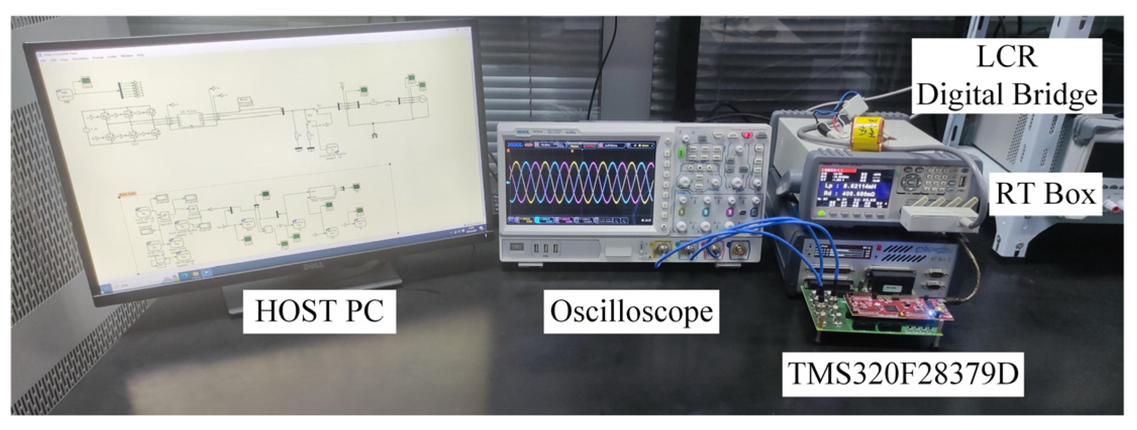
4. Hardware-in-the-Loop Experimental Verification

In order to further verify the effectiveness of the proposed control strategy, a hardware-in-the-loop experimental model of the GFM inverter with a structure corresponding to Figure 1 is constructed. As shown in Figure 7, the hardware-in-the-loop system consists of two parts: the controller and the RT Box. The controller adopts the chip TMS320F28379D control board, which is connected to the RT Box through the interface board, and the sampling data are also sent to the oscilloscope through the ports on the interface board to display the waveforms. The RT Box is a real-time simulator specially designed for power electronics applications. With numerous analog and digital input/output channels and FPGA embedded CPU cores, it is a versatile processing unit for real-time hardware-in-the-loop testing. It is able to perform a real-time simulation of the power stage of a power electronic system and is connected to the host computer through Gigabit Ethernet to realize data interaction.
The main parameters of hardware-in-the-loop are shown in Table 1. The size of the line impedance in the low-voltage micro-network is Rg = 0.642 Ω/km, Xg = 0.083 Ω/km, and the impedance ratio is R/X = 7.7 [37]. The nominal line impedance is selected as the length of the line is 5 km, and the actual line impedance cases are designed as follows: (1) +10% perturbation of the resistance parameter, +10% perturbation of the inductance parameter; (2) +20% perturbation of resistance parameter, +20% perturbation of inductance parameter; (3) +10% perturbation of the resistance parameter, −10% perturbation of the inductance parameter; (4) +20% perturbation of resistance parameter, −20% perturbation of inductance parameter.
The main parameters of the controller are shown in Table 2. In order to ensure a suitable voltage-following capability for output voltage control, it is controlled by inner-loop inductor current P control and outer-loop output voltage PI control. The virtual impedance parameters are designed as Rv = −3 Ω, Lv = 5 mH. When the resistive component of the line impedance is large, it is inappropriate to increase the virtual inductance only by increasing the virtual inductance, and the resistive component of the total equivalent line impedance can be reduced by designing the virtual resistance as a negative value so that the total equivalent line impedance appears to be purely inductive. RT Box can accelerate the simulation using FPGAs. The plant discretization time-step for the experimental model in this paper can be accelerated to 500 ns using FPGAs.

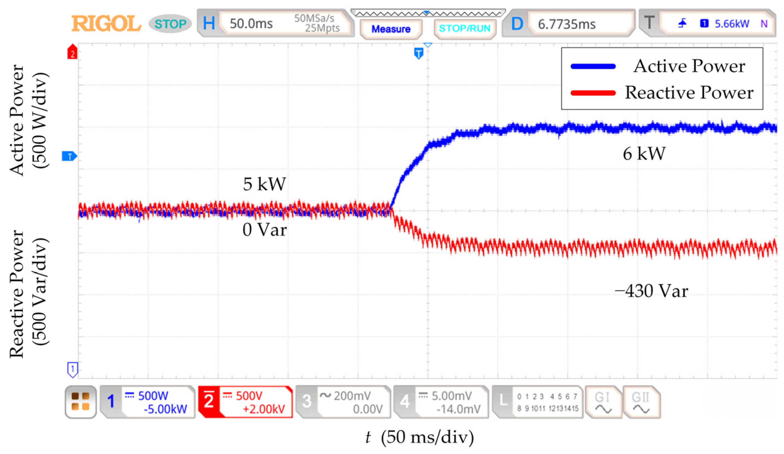
4.1. Verification of the Effect of Line Impedance Parameter Perturbation on Decoupling Ability

Under the initial state, the active power is 5 kW and the reactive power is 0 Var. Figure 8 shows that when the active power setting is increased from 5 kW to 6 kW, the reactive power changes by 1.7 kVar. Since the nominal line impedance is mainly resistive, the power coupling phenomenon is more serious. Figure 9 shows that when using virtual impedance for decoupling, the set value of active power is also increased by 1 kW, and the reactive power only changes by 230 Var, which obviously reduces the coupling between active and reactive power. However, Figure 10 and Figure 11 show that when the GFM inverter is operated at the actual line impedance, the active power set value is increased by the same 1 kW, the reactive power changes 430 Var in Case 1, and the reactive power changes 680 Var in Case 2. It can be seen that the decoupling ability of the virtual impedance method is affected by the line impedance parameter perturbation, which results in the decoupling ability becoming worse. The greater the range of deviation of the impedance parameter, the less effective the decoupling is.

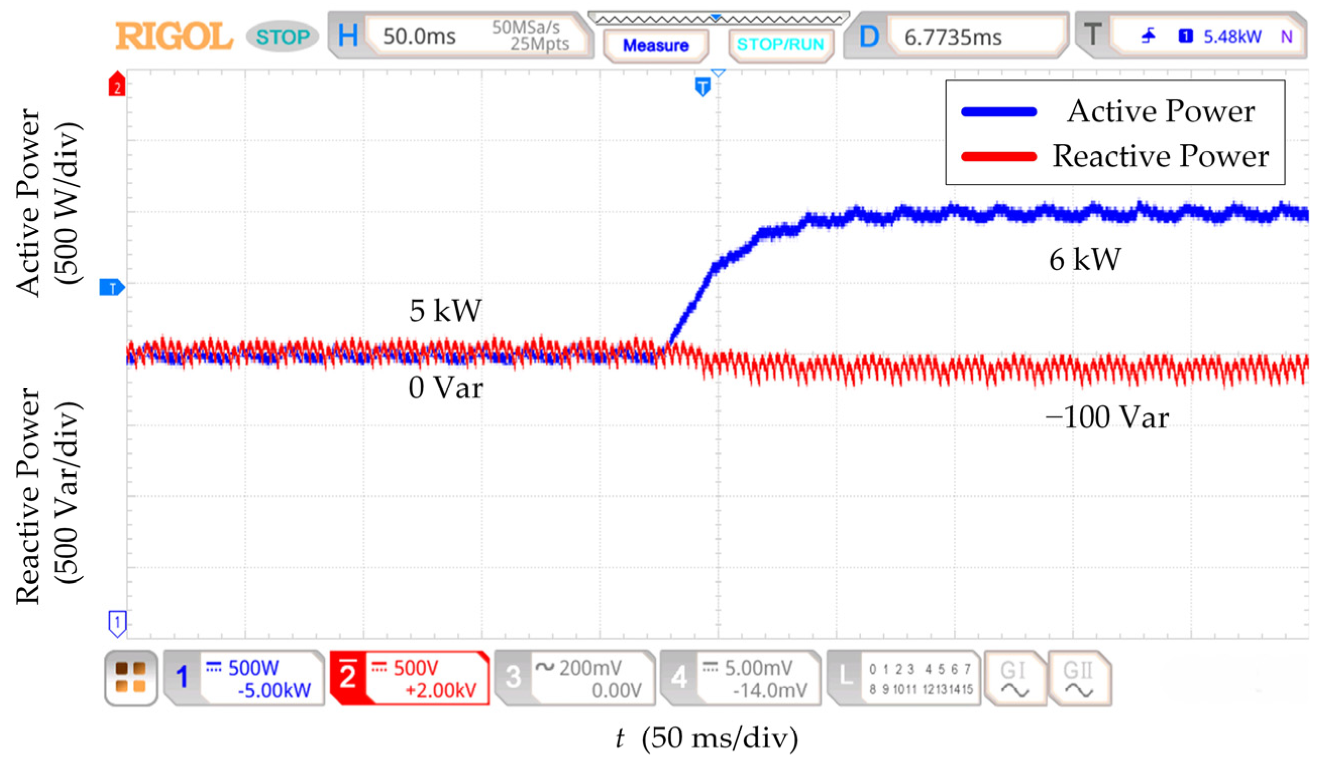
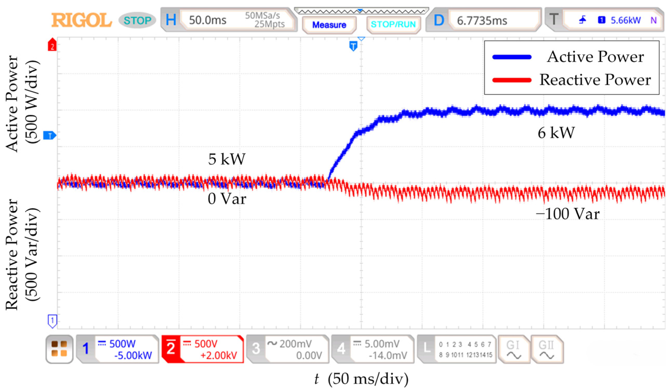
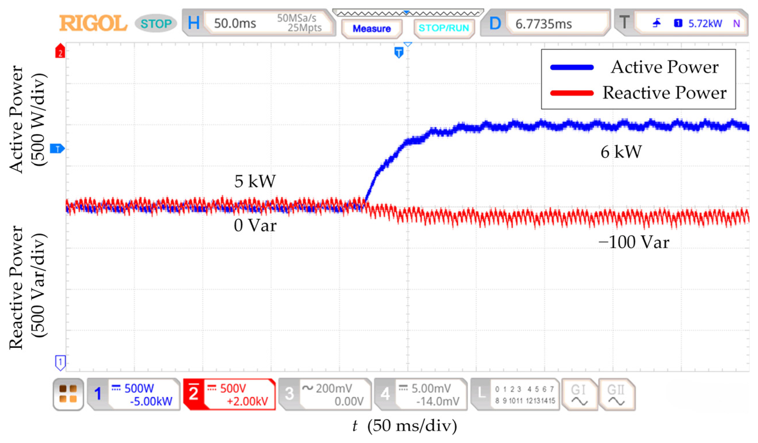
4.2. Verification of ESO-Based Power Decoupling Control Strategy

Under the initial state, the active power is 5 kW, and the reactive power is 0 Var. The parameters of the power decoupling strategy based on RESO are designed at nominal line impedance. Figure 12, Figure 13, Figure 14 and Figure 15 show that the reactive power changes by 100 Var for all four kinds of line impedance parameter perturbation conditions when the active power setpoint is increased from 5 kW to 6 kW. The RESO-based power decoupling strategy has better decoupling capability and more robust decoupling when the line impedance has different sizes of parameter perturbation.

5. Conclusions

In this paper, a power decoupling control strategy based on RESO is proposed in order to improve the robustness of the GFM power decoupling control strategy when line impedance parameter perturbation occurs. The strategy considers the factors affecting the power control performance, such as model deviation and power coupling caused by line impedance parameter perturbation, as internal disturbances. Based on the typical power control strategy and virtual impedance method, these disturbances are observed and compensated in real time by the RESO. The RESO reduces the computing power of the control system and decreases the phase delay of the system. Finally, through RT Box hardware-in-the-loop experimental verification, it is demonstrated that the power decoupling control strategy based on the RESO has better decoupling ability and improves the robustness of the power decoupling control when the line impedance parameter perturbation occurs.

Author Contributions

Conceptualization, M.H.; methodology, M.H. and H.L.; software, M.H.; validation, M.H.; formal analysis, M.H. and H.L.; writing—original draft preparation, M.H.; writing—review and editing, M.H. and H.L.; visualization, M.H.; supervision, M.H. and H.L. All authors have read and agreed to the published version of the manuscript.

Funding

This research was supported by Shanghai Science and Technology Commission Key Program (grant no. 20dz1206100).

Data Availability Statement

Data are unavailable due to privacy.

Conflicts of Interest

All authors claim that this study was conducted without any commercial or financial activities relationships that may be interpreted as potential conflicts of interest.

References

  1. Zhao, G.; Yang, H. Parallel Control of Converters with Energy Storage Equipment in a Microgrid. Electronics 2019, 8, 1110. [Google Scholar] [CrossRef]
  2. Matevosyan, J.; Badrzadeh, B.; Prevost, T.; Quitmann, E.; Ramasubramanian, D.; Urdal, H.; Achilles, S.; MacDowell, J.; Hsien Huang, S.; Vital, V.; et al. Grid-Forming Inverters: Are They the Key for High Renewable Penetration? IEEE Power Energy Mag. 2023, 21, 77–86. [Google Scholar] [CrossRef]
  3. Chen, Y.; Luo, J.; Zhang, X.; Li, X.; Wang, W.; Ding, S. A Virtual Synchronous Generator Secondary Frequency Modulation Control Method Based on Active Disturbance Rejection Controller. Electronics 2023, 12, 4587. [Google Scholar] [CrossRef]
  4. Wang, L.; Zhou, H.; Hu, X.; Hou, X.; Su, C.; Sun, K. Adaptive Inertia and Damping Coordination (AIDC) Control for Grid-Forming VSG to Improve Transient Stability. Electronics 2023, 12, 2060. [Google Scholar] [CrossRef]
  5. Rosso, R.; Wang, X.; Liserre, M.; Lu, X.; Engelken, S. Grid-Forming Converters: Control Approaches, Grid-Synchronization, and Future Trends—A Review. IEEE Open J. Ind. Appl. 2021, 2, 93–109. [Google Scholar] [CrossRef]
  6. Arghir, C.; Jouini, T.; Dörfler, F. Grid-Forming Control for Power Converters Based on Matching of Synchronous Machines. Automatica 2018, 95, 273–282. [Google Scholar] [CrossRef]
  7. Garzon, O.D.; Nassif, A.B.; Rahmatian, M. Grid Forming Technologies to Improve Rate of Change in Frequency and Frequency Nadir: Analysis-Based Replicated Load Shedding Events. Electronics 2024, 13, 1120. [Google Scholar] [CrossRef]
  8. Johnson, B.B.; Sinha, M.; Ainsworth, N.G.; Dörfler, F.; Dhople, S.V. Synthesizing Virtual Oscillators to Control Islanded Inverters. IEEE Trans. Power Electron. 2016, 31, 6002–6015. [Google Scholar] [CrossRef]
  9. Unruh, P.; Nuschke, M.; Strauß, P.; Welck, F. Overview on Grid-Forming Inverter Control Methods. Energies 2020, 13, 2589. [Google Scholar] [CrossRef]
  10. Hu, P.; Jiang, K.; Ji, X.; Cai, Y.; Wang, B.; Liu, D.; Cao, K.; Wang, W. A Novel Grid-Forming Strategy for Self-Synchronous PMSG under Nearly 100% Renewable Electricity. Energies 2023, 16, 6648. [Google Scholar] [CrossRef]
  11. Sun, Z.; Zhu, F.; Cao, X. Study on a Frequency Fluctuation Attenuation Method for the Parallel Multi-VSG System. Front. Energy Res. 2021, 9, 693878. [Google Scholar] [CrossRef]
  12. Shang, L.; Hu, J.; Yuan, X.; Chi, Y.; Tang, H. Modeling and Improved Control of Virtual Synchronous Generators Under Symmetrical Faults of Grid. Zhongguo Dianji Gongcheng Xuebao/Proc. Chin. Soc. Electr. Eng. 2017, 37, 403–411. [Google Scholar] [CrossRef]
  13. Jiang, K.; Liu, D.; Cao, K.; Xiong, P.; Ji, X. Small-Signal Modeling and Configuration Analysis of Grid-Forming Converter under 100% Renewable Electricity Systems. Electronics 2023, 12, 4078. [Google Scholar] [CrossRef]
  14. Song, Z.; Zhang, J.; Tang, F.; Wu, M.; Lv, Z.; Sun, L.; Zhao, T. Small Signal Modeling and Parameter Design of Virtual Synchronous Generator to Weak Grid. In Proceedings of the 2018 13th IEEE Conference on Industrial Electronics and Applications (ICIEA), Wuhan, China, 31 May–2 June 2018; pp. 2618–2624. [Google Scholar]
  15. Wu, H.; Ruan, X.; Yang, D.; Chen, X.; Zhao, W.; Lv, Z.; Zhong, Q.-C. Small-Signal Modeling and Parameters Design for Virtual Synchronous Generators. IEEE Trans. Ind. Electron. 2016, 63, 4292–4303. [Google Scholar] [CrossRef]
  16. Sarojini, R.K.; Palanisamy, K. Small Signal Modelling and Determination of Critical Value of Inertia for Virtual Synchronous Generator. In Proceedings of the 2019 Innovations in Power and Advanced Computing Technologies (i-PACT), Vellore, India, 22–23 March 2019; Volume 1, pp. 1–6. [Google Scholar]
  17. Yu, J.; Qi, Y.; Deng, H.; Liu, X.; Tang, Y. Evaluating Small-Signal Synchronization Stability of Grid-Forming Converter: A Geometrical Approach. IEEE Trans. Ind. Electron. 2022, 69, 9087–9098. [Google Scholar] [CrossRef]
  18. Zhang, L.; Harnefors, L.; Nee, H.-P. Power-Synchronization Control of Grid-Connected Voltage-Source Converters. IEEE Trans. Power Syst. 2010, 25, 809–820. [Google Scholar] [CrossRef]
  19. D’Arco, S.; Suul, J.A.; Fosso, O.B. Small-Signal Modelling and Parametric Sensitivity of a Virtual Synchronous Machine. In Proceedings of the 2014 Power Systems Computation Conference, Wroclaw, Poland, 18–22 August 2014; pp. 1–9. [Google Scholar]
  20. Stankovic, A.M.; Sanders, S.R.; Aydin, T. Dynamic Phasors in Modeling and Analysis of Unbalanced Polyphase AC Machines. IEEE Trans. Energy Convers. 2002, 17, 107–113. [Google Scholar] [CrossRef]
  21. Wu, T.; Liu, Z.; Liu, J.; Wang, S.; You, Z. A Unified Virtual Power Decoupling Method for Droop-Controlled Parallel Inverters in Microgrids. IEEE Trans. Power Electron. 2016, 31, 5587–5603. [Google Scholar] [CrossRef]
  22. De Brabandere, K.; Bolsens, B.; Van den Keybus, J.; Woyte, A.; Driesen, J.; Belmans, R. A Voltage and Frequency Droop Control Method for Parallel Inverters. IEEE Trans. Power Electron. 2007, 22, 1107–1115. [Google Scholar] [CrossRef]
  23. Li, Y.; Li, Y.W. Power Management of Inverter Interfaced Autonomous Microgrid Based on Virtual Frequency-Voltage Frame. IEEE Trans. Smart Grid 2011, 2, 30–40. [Google Scholar] [CrossRef]
  24. Peng, Z.; Wang, J.; Bi, D.; Wen, Y.; Dai, Y.; Yin, X.; Shen, Z.J. Droop Control Strategy Incorporating Coupling Compensation and Virtual Impedance for Microgrid Application. IEEE Trans. Energy Convers. 2019, 34, 277–291. [Google Scholar] [CrossRef]
  25. Peng, Z.; Wang, J.; Wen, Y.; Bi, D.; Dai, Y.; Ning, Y. Virtual Synchronous Generator Control Strategy Incorporating Improved Governor Control and Coupling Compensation for AC Microgrid. IET Power Electron. 2019, 12, 1455–1461. [Google Scholar] [CrossRef]
  26. Li, C.; Yang, Y.; Mijatovic, N.; Dragicevic, T. Frequency Stability Assessment of Grid-Forming VSG in Framework of MPME With Feedforward Decoupling Control Strategy. IEEE Trans. Ind. Electron. 2022, 69, 6903–6913. [Google Scholar] [CrossRef]
  27. Rathnayake, D.B.; Bahrani, B. Multivariable Control Design for Grid-Forming Inverters with Decoupled Active and Reactive Power Loops. IEEE Trans. Power Electron. 2023, 38, 1635–1649. [Google Scholar] [CrossRef]
  28. Guerrero, J.M.; de Vicuna, L.G.; Matas, J.; Castilla, M.; Miret, J. Output Impedance Design of Parallel-Connected UPS Inverters with Wireless Load-Sharing Control. IEEE Trans. Ind. Electron. 2005, 52, 1126–1135. [Google Scholar] [CrossRef]
  29. Rodríguez-Cabero, A.; Roldán-Pérez, J.; Prodanovic, M. Virtual Impedance Design Considerations for Virtual Synchronous Machines in Weak Grids. IEEE J. Emerg. Sel. Top. Power Electron. 2020, 8, 1477–1489. [Google Scholar] [CrossRef]
  30. Wen, T.; Zhu, D.; Zou, X.; Jiang, B.; Peng, L.; Kang, Y. Power Coupling Mechanism Analysis and Improved Decoupling Control for Virtual Synchronous Generator. IEEE Trans. Power Electron. 2021, 36, 3028–3041. [Google Scholar] [CrossRef]
  31. He, J.; Li, Y.W. Analysis, Design, and Implementation of Virtual Impedance for Power Electronics Interfaced Distributed Generation. IEEE Trans. Ind. Appl. 2011, 47, 2525–2538. [Google Scholar] [CrossRef]
  32. Wang, Y.; Wai, R.-J. Newly-Designed Power Decoupling Strategy for Virtual Synchronous Generator in Micro-Grid. In Proceedings of the 2021 IEEE International Future Energy Electronics Conference (IFEEC), Taipei, Taiwan, 16–19 November 2021; pp. 1–6. [Google Scholar]
  33. Wang, Y.; Wai, R.-J. Adaptive Fuzzy-Neural-Network Power Decoupling Strategy for Virtual Synchronous Generator in Micro-Grid. IEEE Trans. Power Electron. 2022, 37, 3878–3891. [Google Scholar] [CrossRef]
  34. Dong, N.; Li, M.; Chang, X.; Zhang, W.; Yang, H.; Zhao, R. Robust Power Decoupling Based on Feedforward Decoupling and Extended State Observers for Virtual Synchronous Generator in Weak Grid. IEEE J. Emerg. Sel. Top. Power Electron. 2023, 11, 576–587. [Google Scholar] [CrossRef]
  35. Han, J. From PID to Active Disturbance Rejection Control. IEEE Trans. Ind. Electron. 2009, 56, 900–906. [Google Scholar] [CrossRef]
  36. Fu, C.; Tan, W. Parameters Tuning of Reduced-Order Active Disturbance Rejection Control. IEEE Access 2020, 8, 72528–72536. [Google Scholar] [CrossRef]
  37. Engler, A.; Soultanis, N. Droop Control in LV-Grids. In Proceedings of the 2005 International Conference on Future Power Systems, Amsterdam, The Netherlands, 18 November 2005; p. 6. [Google Scholar]
Figure 1. Main circuit topology and typical control block diagram of GFM inverter.
Electronics 13 01926 g001
Figure 2. Grid-connected equivalent circuit diagram of GFM.
Electronics 13 01926 g002
Figure 3. GFM power small-signal model (considering virtual impedance).
Electronics 13 01926 g003
Figure 4. Simplified control block diagram of GFM power decoupling based on RESO.
Electronics 13 01926 g004
Figure 5. Frequency domain analysis of observation capabilities of different ESOs.
Electronics 13 01926 g005
Figure 6. Frequency domain analysis of RESO observation capability for different bandwidths.
Electronics 13 01926 g006
Figure 7. Hardware-in-the-loop experimental platform.
Electronics 13 01926 g007
Figure 8. Without power decoupling (running at nominal line impedance).
Electronics 13 01926 g008
Figure 9. Power decoupling with virtual impedance method (running at nominal line impedance).
Electronics 13 01926 g009
Figure 10. Power decoupling with virtual impedance method (running at actual line impedance Case 1).
Electronics 13 01926 g010
Figure 11. Power decoupling with virtual impedance method (running at actual line impedance Case 2).
Electronics 13 01926 g011
Figure 12. Power decoupling strategy based on RESO (running at actual line impedance Case 1, P change of 1 kW).
Electronics 13 01926 g012
Figure 13. Power decoupling strategy based on RESO (running at actual line impedance Case 2, P change of 1 kW).
Electronics 13 01926 g013
Figure 14. Power decoupling strategy based on RESO (running at actual line impedance Case 3, P change of 1 kW).
Electronics 13 01926 g014
Figure 15. Power decoupling strategy based on RESO (running at actual line impedance Case 4, P change of 1 kW).
Electronics 13 01926 g015
Table 1. Hardware-in-the-loop main parameter.
ParametersValue/Unit
Grid phase voltage (RMS)220 V
DC bus voltage750 V
Grid frequency50 Hz
Inverter side inductance2 mH
Network side inductance0.4 mH
Filter capacitor2.2 uF
Nominal line inductance1.32 mH
Nominal line resistance3.21 Ω
Switching frequency100 kHz
Plant discretization time-step500 ns
Table 2. Controller parameter.
ParametersValue
Current inner-loop proportional gain5
Voltage outer-loop proportional gain0.01
Voltage outer-loop integration gain300
Active power observer bandwidth700 rad/s
Reactive power observer bandwidth500 rad/s
Virtual inductors5 mH
Virtual resistors−3 Ω
Virtual inertia factor for active power0.04
Active droop factor10.07
Virtual inertia factor for reactive power5
Reactive droop factor321.5
Disclaimer/Publisher’s Note: The statements, opinions and data contained in all publications are solely those of the individual author(s) and contributor(s) and not of MDPI and/or the editor(s). MDPI and/or the editor(s) disclaim responsibility for any injury to people or property resulting from any ideas, methods, instructions or products referred to in the content.

