Article

A Procedure for Precise Determination and Compensation of Lead-Wire Resistance of a Two-Wire Resistance Temperature Detector

by
Apinai Rerkratn
1,
Supatsorn Prombut
1,
Thawatchai Kamsri
2,
Vanchai Riewruja
1,* and
Wandee Petchmaneelumka
1,*
1
School of Engineering, King Mongkut’s Institute of Technology Ladkrabang, Bangkok 10520, Thailand
2
Thai Microeletronics Center (TMEC), Chachoengsao 24000, Thailand
*
Authors to whom correspondence should be addressed.
Sensors 2022, 22(11), 4176; https://doi.org/10.3390/s22114176
Submission received: 12 April 2022 / Revised: 26 May 2022 / Accepted: 27 May 2022 / Published: 31 May 2022
(This article belongs to the Special Issue Intelligent Circuits and Sensing Technologies)

Abstract

:
A procedure for the precise determination and compensation of the lead-wire resistance of a resistance transducer is presented. The proposed technique is suitable for a two-wire resistance transducer, especially the resistance temperature detector (RTD). The proposed procedure provides a technique to compensate for the lead-wire resistance using a three-level pulse signal to excite the RTD via the long lead wire. In addition, the variation in the lead-wire resistance disturbed by the change in the ambient temperature can also be compensated by using the proposed technique. The determination of the lead-wire resistance from the proposed procedure requires a simple computation method performed by a digital signal processing unit. Therefore, the calculation of the RTD resistance and the lead-wire resistance can be achieved without the requirement of a high-speed digital signal processing unit. The proposed procedure is implemented on two platforms to confirm its effectiveness: the LabVIEW computer program and the microcontroller board. Experimental results show that the RTD resistance was accurately acquired, where the measured temperature varied from 0 °C to 300 °C and the lead-wire resistance varied from 0.2 Ω to 20 Ω, corresponding to the length of the 26 American wire gauge (AWG) lead wire from 1.5 m to 150 m. The average power dissipation to the RTD was very low and the self-heating of the RTD was minimized. The measurement error of the RTD resistance observed for pt100 was within ±0.98 Ω or ±0.27 °C when the lead wire of 30 m was placed in an environment with the ambient temperature varying from 30 °C to 70 °C. It is evident that the proposed procedure provided a performance that agreed with the theoretical expectation.

1. Introduction

Temperature is the most monitored and controlled variable in industrial control systems. A temperature sensor plays the important role in industrial applications of maintaining a certain temperature for a specific process. There are several common types of temperature sensors used in industrial process applications, such as a negative coefficient thermistor (NTC), resistance temperature detector (RTD), thermocouple, and semiconductor junction-based sensor [1,2,3]. The NTC, thermocouple, and semiconductor junction-based sensor require a complex signal conditioning circuit to measure the temperature. The RTD is a passive sensor and produces a positive variation in its resistance to the variation of ambient temperature. The RTD is constructed from platinum wire, which provides distinctive behaviors in terms of high accuracy, high linearity, high stability, and a low hysteresis effect [4,5,6]. In industrial applications, the RTD has become the most considered sensor for temperature measurement due to its behaviors. The distance from the RTD sensor to the signal conditioning circuit requires a long-range lead wire, which is considered as the parasitic resistance for each lead wire. The lead-wire resistance of the wire connected from the RTD to the control station includes the RTD resistance. This is introduced as a large error of temperature measurement in the industrial process. Moreover, the change in the ambient temperature causes variation in the lead-wire resistance due to the thermal property of the metals used for the lead wire, which causes an uncertain error in the measured temperature quantity. If the lead-wire resistance of about 1 Ω is added to the RTD resistance, then the measured temperature error occurs at about 2.4 °C for a pt100 two-wire RTD [7,8,9,10,11]. In addition, the contact resistance of the terminal between the control station and the RTD is added to the lead-wire resistance. The contact resistance including the lead-wire resistance is collectively called the lead-wire resistance in this paper. A drawback of the RTD sensor is the lead-wire resistance, which can be compensated using the RTD with three or four lead wires [2,3,4,5,12,13]. The range of all the lead wires is set to equal, which provides equal lead-wire resistance. Usually, the determination of the process temperature is based on the use of a bridge circuit [1,2,3,11,13,14,15]. A disadvantage of the bridge circuit is that the signal readout directly from the bridge circuit is nonlinear. The technique for a linear readout of the signal from the bridge circuit using a microcontroller and relaxation oscillator is proposed in the literature [10]. The compensation of the lead-wire resistance using a three- or four-wire RTD is also proposed in the recent literature [12,16]. These techniques require several amplifiers and a current source, which adds complexity to the signal conditioning circuit. However, the compensation of lead-wire resistance for three- and four-wire RTDs is efficient only when there is equal resistance in each lead wire. In addition, the RTD with three or four lead wires increases the cost and complexity of the control system, especially for the remote measurement and the multipoint measurements. Therefore, the use of a two-wire RTD sensor is a simple and economical attraction. There are many techniques to reduce the error due to the lead-wire resistance, including the contact resistance of the two-wire resistive sensor, proposed in the literature [7,8,9,10,13,17]. An approach to compensate for the error caused by the lead-wire in a two-wire RTD using a precision shunt voltage reference and current source is proposed in [18]. This technique provides two kinds of excitation signals, a voltage signal and a current signal, for the RTD. The voltage signal from the precision voltage reference of this approach is used to measure the lead-wire resistance, whereas the current signal from the current source is used to obtain the resistance of the RTD, including the lead-wire resistance. Unfortunately, the high magnitude of the voltage signal across the RTD during the lead-wire resistance measurement causes a self-heating effect in the RTD. Therefore, this approach is suitable for when the RTD has a high resistance, such as the pt1000 RTD has, to reduce the current flowing through the RTD. Other approaches based on two diodes acting as an electronic switch connected to the terminal of the RTD to measure the lead-wire resistance are proposed in the recent literature [7,8,9,10,18]. The operation of these approaches is based on the relaxation oscillator and microcontroller. These approaches require the bidirectional current signal to obtain the resistance of the RTD. However, the threshold voltage of the diodes must be equal to avoid the error of the measured variable. For the mismatch of a diode threshold voltage of about 1 mV, the measured error of about 2.5 °C was observed for the pt100 RTD with a 1 mA excitation current [11]. Furthermore, the diode threshold voltage is dependent on the variation in the ambient temperature due to the thermal voltage that is characteristic of diodes. This error becomes a significant parameter, same as the lead-wire resistance. To avoid the error mentioned above, closely matched diodes are required. Unfortunately, the closely matched diodes are impossible for discrete devices. The technique using two diodes is low cost and simple without using specific devices. If the threshold voltage of the diode can be compensated for, then the advantage of this technique will be gained.
In this paper, the procedure to determine and compensate for the lead-wire resistance and the resistance of the RTD using two diodes is proposed. The lead-wire resistance, the RTD resistance, and the diode threshold voltage are accurately determined. The effect of the mismatch of the diodes in terms of the threshold voltage can be prevented with the proposed technique. The proposed procedure provides the bidirectional current signal with three-step pulse levels in the amplitude of the series to excite the RTD sensor. The amplitude of each step of the current signal is doubled in the amplitude of the series. The RTD resistance, the lead-wire resistance, and the diode threshold voltage are determined via a digital signal processing unit using the simple mathematic operations add and subtract. Therefore, the operation time of the proposed procedure is fast and accurate. The proposed procedure is implemented to confirm the accuracy and performance using commercial devices. The temperature readout from the proposed technique exhibits that a maximum error of about 0.27 °C is observed, where the ambient temperature varies from 30 °C to 70 °C. It should be noted that the proposed technique can be applied to many types of resistive sensors in related fields such as civil engineering [19,20,21,22,23,24], automobile engineering [25,26], and mechanical engineering [27], and in the use of scientific and medical equipment [3,4,5,6,28], to measure the quantity of gas, humidity, airflow, force, pressure, and strain. For the example of the application in the field of civil engineering, the resistive sensors are provided for the measurement of the structural parameters to evaluate the structural behaviors of the structural health monitoring system [19,20,21,22,23,24]. In addition, the proposed technique can be applied to investigate the behaviors of construction materials such as fly-ash-based concrete and non-autoclaved silicate materials [29,30]. The resistance readout from the resistive sensor requires an accurate value to make a decision regarding the safety of civil infrastructure [20,24]. Therefore, the proposed technique is suitable for this requirement. The organization of this paper is divided into five sections as follows: Section 2 introduces a conventional technique to compensate for the lead-wire resistance. The proposed procedure and circuit to determine the resistance of the lead wire and the RTD using a three-step pulse signal are also presented in this section. In Section 3, the accuracy of the proposed circuit is analyzed and discussed in detail. Section 4 describes the experimental results of the proposed procedure using two signal processing units. The first signal processing unit is the LabVIEW computer-based program interfaced with an analog input/output board. Another signal processing unit is a microcontroller board. Finally, the conclusion of this paper is described in Section 5.

2. Principle of the Proposed Procedure

The accuracy of the temperature measurement using the RTD is disturbed by the parasitic resistance of the lead wire. The resistance readout from the RTD includes the lead-wire resistance. In addition, the lead-wire resistance is dependent on the change in the ambient temperature, which can cause an uncertain readout of the resistance from the RTD. The compensation of the lead-wire resistance using two diodes is a useful technique and the procedure for determining the lead-wire resistance is described in this section.

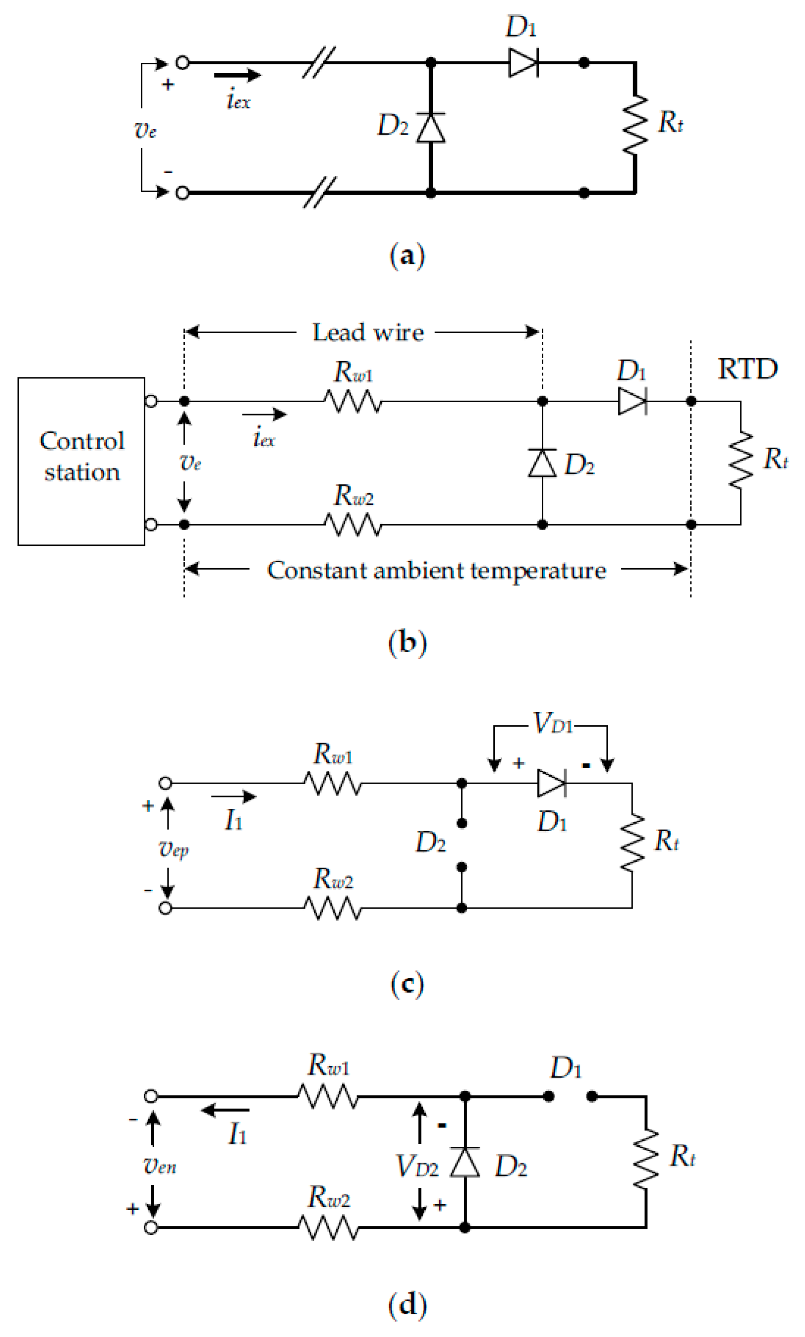
2.1. Conventional Procedure

A diagram of the RTD connected with two diodes is shown in Figure 1a, where Rt is the RTD resistance [7,8,9,10,17]. Two diodes are laid close to the terminals of the RTD to ignore the wiring resistance between the RTD resistance Rt and the diodes. The lead-wire resistance is determined from the RTD to the control station as shown in Figure 1b, where Rw1 and Rw2 are the intrinsic resistances of two lead wires. For recent approaches, the voltages across the diodes D1 and D2 were assumed to be equal. The lead-wire resistance was compensated for in these approaches using bidirectional excitation current iex. From Figure 1c, the excitation current iex = I1 is applied; then, the diodes D1 and D2 are conducted and turned off, respectively, as shown in Figure 1c. The relationship between the voltage signal vep and the excitation current iex can be given by:
v e p = I 1 R t + I 1 R w 1 + I 1 R w 2 + V D 1
where VD1 is the voltage across the diode D1. For the excitation current iex = −I1, the operations of the diodes D1 and D2 are opposite from the previous state, as shown in Figure 1d. Therefore, the voltage ven can be stated as:
v e n = I 1 R w 1 + I 1 R w 2 + V D 2
where VD2 is the voltage across the diode D2. If the closely matched diodes are chosen for diodes D1 and D2, then VD1 = VD2 is obtained. Practically, the intrinsic resistances Rw1 and Rw2 are equal due to the same length of the two lead wires. Therefore, the RTD resistance Rt can be simply obtained by the subtraction of Equations (1) and (2) as:
R t = ( v e p v e n ) I 1
It should be noted that the RTD resistance of Equation (3) is accurately determined only for the constant ambient temperature of the lead wire and the diodes in Figure 1b. In addition, the mismatch of the diodes causes the incomplete cancellation of the voltage across the diodes D1 and D2. The voltage VD across the diode is dependent on the ambient temperature and can be expressed as:
V D = η k T q ln I D I S
where η and IS are the empirical constant and the reverse saturated current of the diode, respectively, k = 1.38 × 10²³ J/K is the Boltzmann constant, q = 1.602 × 10¹⁹ C is the electron charge, and T = (273 + °C) is the absolute temperature in Kelvin. It should be noted that the term kT/q is usually called the thermal voltage VT [31]. The thermal voltage VT is approximated as 25.67 mV at 25 °C of the ambient temperature. In Equation (4), the mismatched diodes are exhibited in terms of the reverse saturated current IS of each diode. Practically, the perfectly matched diodes are not enough in the discrete device and also in the integrated circuit form. In Equation (3), the incomplete cancellation of the diode voltages VD1 and VD2 causes the calculation error of the resistance Rt. The voltage across the diode can be accurately determined using the proposed procedure. Therefore, the requirement of perfectly matched diodes is unnecessary.

2.2. Proposed Procedure

To determine the voltage across diodes VD1 and VD2, the current signal in the form of a three-step pulse signal is provided to excite the RTD as shown in Figure 2a. Each step of the current signal is double the previous current quantity. All resistances in the current signal path can also be simply determined. The circuit diagram for the operation of the proposed procedure is shown in Figure 2b. In Figure 2b, the three-step pulse signal is simplified by three current sources for the explanation of the circuit operation. The microprocessor and controller unit (MCU) is used for the digital signal processing and controlling the analog switch SC to generate the three-step pulse signal. The operation of the circuit diagram in Figure 2b can be considered in two stages of the excitation signals: stage I for the positive current signal and stage II for the negative current signal. For stage I of the procedure, the magnitude I1 of the excitation current iex in the second step in Figure 2a is set as the reference current. The current magnitudes of the first step and third step are assigned to equal I1/2 and 2I1, respectively. An operating diagram for stage I is shown in Figure 2c. In Figure 2c, the diodes D1 and D2 are conduct and cutoff, respectively. For the first step of the excitation current iex = I1/2, the voltage vep1 can be stated as:
v e p 1 = ( R w 1 + R w 2 + R t ) I 1 2 + V D 1 = ( R w 1 + R w 2 + R t ) I 1 2 + η V T ln I 1 2 I S 1
where IS1 denotes the reverse saturated current of the diode D1. The voltage vep1 is converted to digital form by an analog-to-digital converter (ADC) and transferred to the MCU. For the second step of the excitation current iex = I1, the voltage vep2 can be given by:
v e p 2 = ( R w 1 + R w 2 + R t ) I 1 + η V T ln I 1 I S 1
The voltage vep22 is assigned as double the magnitude of the voltage vep2, which is calculated by the MCU. Therefore, the voltage vep22 can be written as:
v e p 22 = 2 ( R w 1 + R w 2 + R t ) I 1 + 2 η V T ln ( I 1 I S 1 )
It should be noted that doubling the voltage across diode VD1, written as 2VD1, corresponds to the term of ηVTln(I1/IS1)2. Therefore, Equation (7) can be rewritten as:
v e p 22 = 2 ( R w 1 + R w 2 + R t ) I 1 + η V T ln ( I 1 I S 1 ) 2
For the third step, the excitation current iex = 2I1 is set. Then, the voltage vep3 can be expressed as:
v e p 3 = 2 ( R w 1 + R w 2 + R t ) I 1 + η V T ln 2 I 1 I S 1
From Equations (8) and (9), the subtraction result veps1 of the voltages vep22 and vep3 can be given by:
v e p s 1 = η V T ( ln ( I 1 I S 1 ) 2 ln ( 2 I 1 I S 1 ) ) = η V T ln I 1 2 I S 1
To subtract Equation (5) by Equation (10), the resulting voltage veps2 can be given as:
v e p s 2 = I 1 2 R t + I 1 2 ( R w 1 + R w 2 )
Equations (10) and (11) exhibit only the voltage across diode VD1 and all resistances in the current path, respectively. Practically, the resistances Rw1 = Rw2 = Rw are assigned due to the same length of the lead wire. Therefore, Equation (11) can be rewritten as:
v e p s 2 = I 1 2 R t + I 1 R w
The resistance Rw can be obtained by stage II of the proposed procedure. The operating circuit for stage II is shown in Figure 2d. The magnitude of the excitation current iex for stage II is set as a negative current. Therefore, the magnitudes of the excitation currents of each step are set as –I1/2, −I1, and −2I1. From Figure 2d, the excitation current iex = I1/2 is applied, which forces the diodes D1 and D2 to cutoff and conduct, respectively. Therefore, the voltage ven1 across nodes X and Y can be given by:
v e n 1 = I 1 R w + η V T ln ( I 1 2 I S 2 )
where IS2 is the reverse saturated current of the diode D2. As the same with stage I, the voltage ven2 can be expressed for the excitation current iex = −I1 in the second step as:
v e n 2 = 2 I 1 R w + η V T ln ( I 1 I S 2 )
The voltage ven2 in Equation (14) is multiplied by two as:
v e n 22 = 2 v e n 2 = 4 I 1 R w + η V T ln ( I 1 I S 2 ) 2
For the excitation current iex = −2I1 in the third step, the voltage ven3 across nodes X and Y can be stated as:
v e n 3 = 4 I 1 R w + η V T ln ( 2 I 1 I S 2 )
The subtraction result vens1 of the Equations (15) and (16) can be given by:
v e n s 1 = η V T ( ln ( I 1 I S 2 ) 2 ln ( 2 I 1 I S 2 ) ) = η V T ln ( I 1 2 I S 2 )
From Equation (17) the voltage VD2 across diode D2 is obtained. The diode voltage VD2 is subtracted from Equation (13) as:
v e n s 2 = v e n 1 v e n s 1 = I 1 R w
From Equation (18), the lead-wire resistance Rw = vens2/I1 is obtained. It should be noted that the RTD resistance Rt can be achieved by substituting Equation (18) in Equation (12) as:
R t = 2 ( v e p s 2 v e n s 2 ) I 1
The advantage of the proposed procedure is that the RTD resistance Rt, the resistances Rw1 = Rw2, and the diode voltages VD1 and VD2 can be accurately determined.

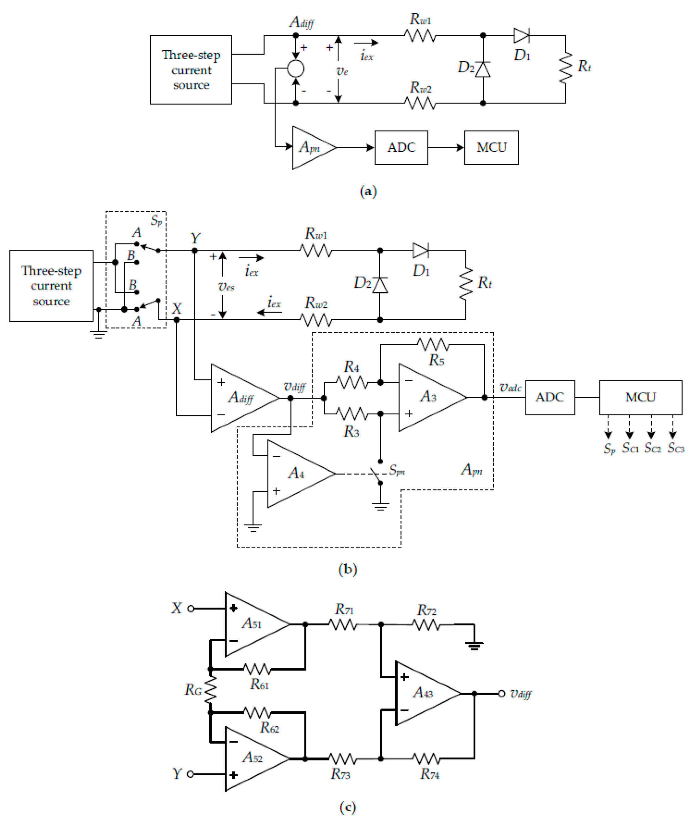
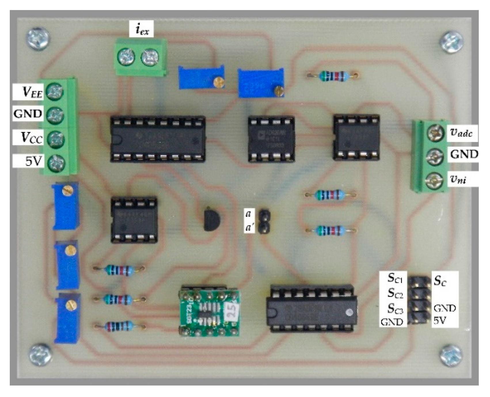
2.3. Implementation of the Proposed Procedure

The proposed procedure is realized using a mixed-signal circuit technique, which contains both analog and digital properties. The three-step pulse signal of Figure 2a can be realized as shown in Figure 3, which is separated into two parts, a three-step voltage source and a voltage-to-current converter. The voltage-to-current converter, shown on the right side of the circuit in Figure 3, consists of an operational amplifier (opamp) A1, transistor Q1, and resistors R1, R2, and RC. From the routine circuit analysis, the relationship between the excitation current iex and the voltage Vref can be expressed as:
i e x = R 2 R 1 R C V r e f + V C C R C ( R 1 + R 2 ) R 1 R C V o f
where VCC is the power-supply voltage of the opamp A1. From Equation (20), if the conditions of R1 = R2, Vof = VCC/2, and R2 >> RC are fulfilled, then the excitation current iex can be stated as:
i e x = V r e f R C
From Equation (21), the current quantity of each step of the excitation current iex can be obtained by changing the reference voltage Vref to an appropriate value. The reference voltage Vref in Equation (21) is provided from the three-step voltage source on the left side of the circuit in Figure 3.
The analog switches SC1, SC2, and SC3, and the resistances Rr1, Rr2, and Rr3 are one-by-one controlled by the MCU to achieve the currents for each step. The voltage source VS provides the constant voltage to generate the reference voltage Vref. The opamp A2 acts as the voltage follower used to prevent the loading effect. For the proposed procedure, the resistances Rr1 to Rr3 are successively connected by means of the MCU-controlled analog switches SC1, SC2, and SC3 to provide the magnitude of each step for the excitation current iex as I1/2, I1, and 2I1. The reference voltage Vref can be simply calculated as:
V r e f i = R r i V S ( R r f + R r i )   for i = 1 ,   2 ,   3
The voltage Vref is applied to the voltage-to-current converter to generate the three-step current signal. Therefore, the excitation currents iex of each step, I1/2, I1, and 2I1, are obtained.
The block diagram of the proposed circuit technique is shown in Figure 4a. As seen in Figure 4a, the analog signal circuit consists of the three-step current source, the difference amplifier Adiff, and the phase-inversion-switched amplifier Apn [32].
The digital signal circuit comprises the analog-to-digital converter (ADC) and the MCU, where both ADC and MCU are integrated into the microcontroller board for practical implementation. The simplified diagram of the proposed procedure is shown in Figure 4b. In Figure 4b, the set of an analog switch unit SP is used to control the flow direction of the excitation current iex. The operation of the diagram in Figure 4b can be explained as follows. For stage I of the proposed procedure, the MCU controls the switch unit SP and sets to the position “A”. The excitation current iex flows through the resistance Rw1, the diode D1, the resistance Rt, and the resistance Rw2. In Figure 4b, the analog voltage ves is amplified to a proper value by the difference amplifier Adiff. The schematic diagram of the difference amplifier Adiff is shown in Figure 4c. From Figure 4c, the resistances R61 = R62 = R6 and R71 = R72 = R73 = R74 = R7 are assigned. Then, output signal vdiff of the difference amplifier Adiff can be expressed as [28,33]:
v d i f f = ( 1 + 2 R 6 R G ) v e s = G a v e s
The phase-inversion-switched amplifier Apn, consisting of the opamps A3 and A4, the resistors R3 to R5, and analog switch Spn, is provided to invert the negative voltage signal vdiff of the second stage of the proposed procedure to the positive voltage signal for the ADC. The opamp A4 acts as a comparator to investigate the polarity of the voltage signal ves. If the voltage signal ves is positive for stage I and the switch Spn is controlled to “open” by the opamp A4, then the phase-inversion-switched amplifier Apn is formed as the noninverting amplifier with unity gain. For stage II, the voltage signal ves is negative and the switch Spn is controlled to “close” by the opamp A4. Therefore, the phase-inversion-switched amplifier Apn acts as the inverting amplifier with unity gain. The transfer characteristic of the phase-inversion-switched amplifier Apn can be expressed as:
v a d c = { G a v e s i G a v e s i f o r v e s i > 0 f o r v e s i < 0
where i = 1, 2, 3 for the signal currents I1/2, I1, and 2I1. The voltage signals ves1, ves2, and ves3 of each step are successively obtained and transferred to the MCU. In the same way, the analog switch unit SP is controlled by MCU to position “B”, which causes the excitation current iex to flow in the opposite direction. The excitation current iex flows through the resistance Rw2, the diode D2, and the resistance Rw1. Each step of the voltage signals ves1 to ves3 is sequentially transferred to the MCU. Therefore, the resistances Rw1, Rw2, and the voltage across the diode D2 in the excitation current path are determined by the proposed procedure mentioned in Section 2.2.

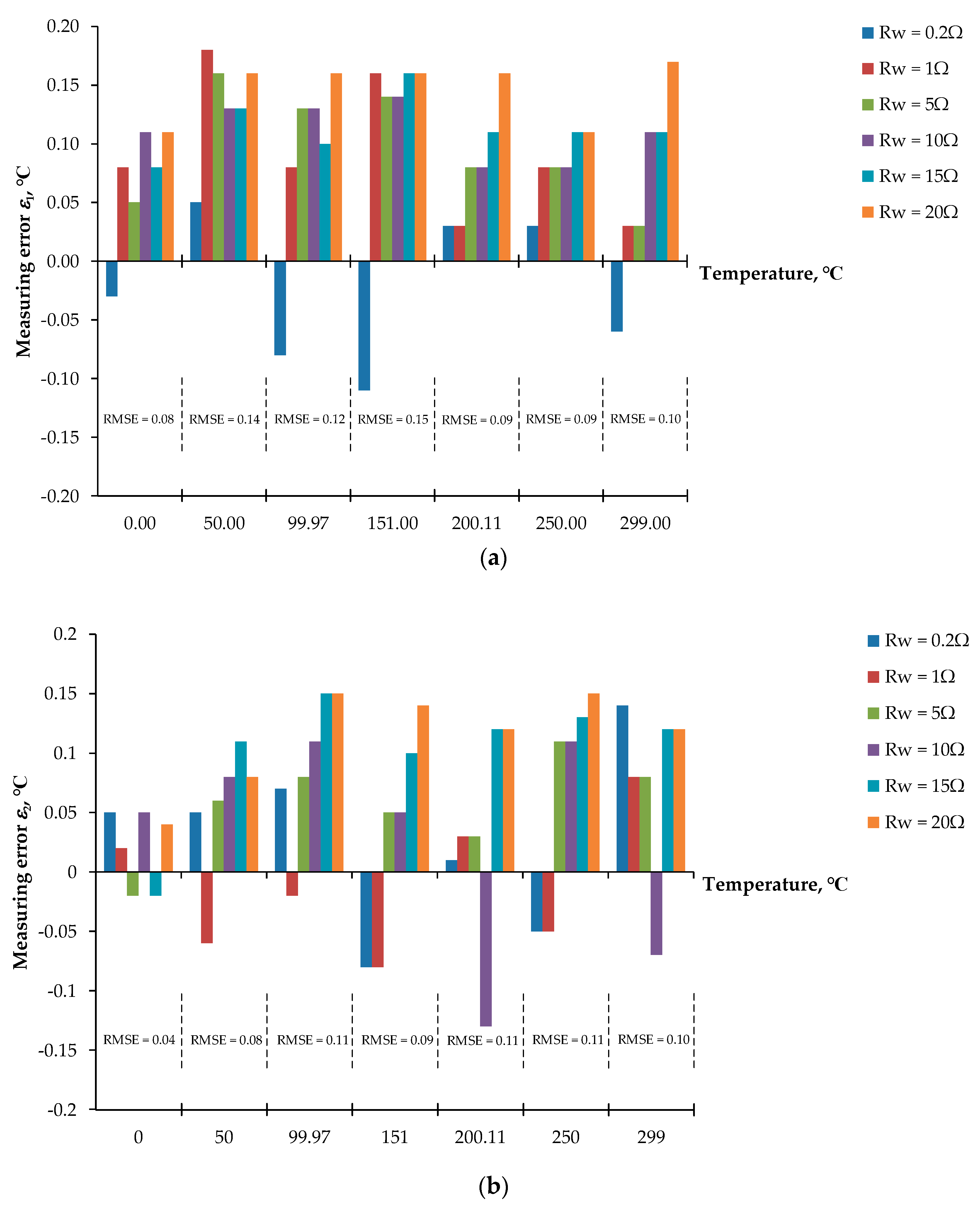
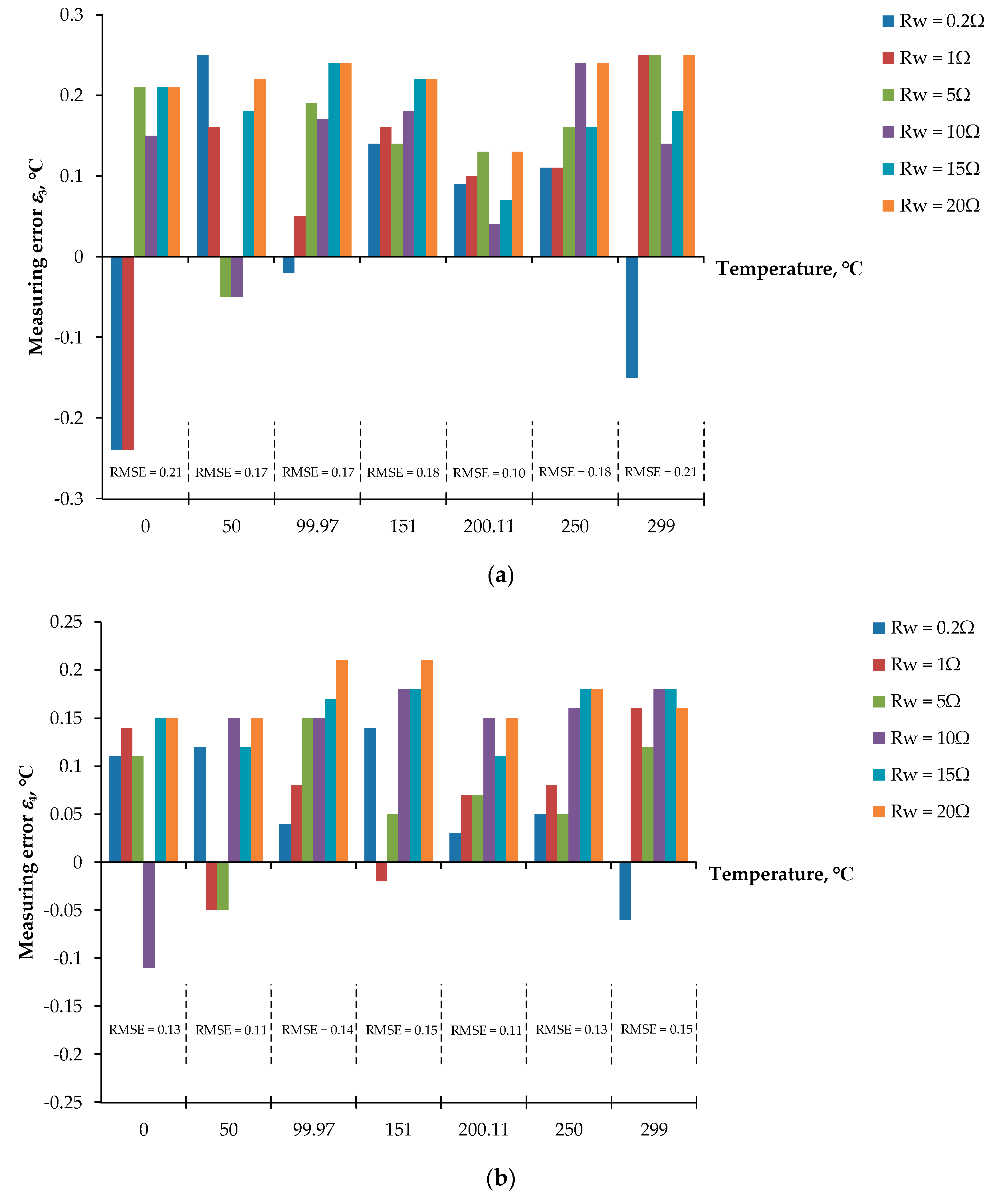
3. Performance Analysis

The accuracy of the proposed technique to determine the lead-wire resistance, the RTD resistance, and the voltage across the diode can be disturbed by the nonideal characteristic of the devices used in the experimental circuit. There are three major factors that cause an error in the proposed technique. The first factor, the derivation from the expected magnitude of the excitation current iex for each step in stage I and stage II, causes an inaccuracy of the calculated resistances and diode voltages in the proposed procedure. For the voltage-to-current converter circuit in Figure 3, the tolerance of the resistors used in the experimental circuit causes an error on the excitation current iex. From Equation (20), the relationship between the current iex and the reference voltage source Vref including the tolerance of the resistors can be approximately given by:
i e x = ( 1 ε i ) V r e f R C + I o f f s e t
ε i = Δ R ( 1 + Δ R 2 )
I o f f s e t = V C C R C ( 2 + Δ R ) ( 1 + Δ R 2 ) V o f R C
where ΔR denotes the tolerance of the resistor. From Equation (25), the tolerance ΔR of the resistors causes the error εi on the converted current iex in the first term on the right. This error can be avoided by replacing the resistor R1 in Figure 3 with the variable resistor and fine-tuning the resistance to match the resistance R2. In addition, the offset current Ioffset in Equation (27) can be canceled by adjusting the voltage Vof to an appropriate value. The second factor, the gain error of the phase-inversion-switched amplifier in Figure 4c causes the error in the voltage signal vadc. The voltage signal vadc, from the phase-inversion-switched amplifier for the resistors R3 and R4 having the tolerance ΔP, can be approximated as:
v a d c = { ( 1 + 3 Δ P 2 ) ( 1 + Δ P 2 ) G a v e s f o r v e s > 0 ( 1 Δ P 2 ) ( 1 + Δ P 2 ) G a v e s f o r v e s < 0
In Equation (28), the closely matched selection of the resistors R3 and R4 can minimize the gain error of the phase-inversion-switched amplifier. The third factor is when the gain error occurs due to the mismatched resistors in the schematic diagram of the difference amplifier Adiff. However, the difference amplifier Adiff used for the experiment in this paper is commercially available, and the resistances in the schematic circuit are trimmed by laser to ensure the closely matched resistors [33]. Therefore, the gain error is very small and too insignificant to disturb the performance of the experimental implementation in this paper. It should be noted that the contact resistance of the analog switch unit SP is unaffected by the signal ves transferred to the difference amplifier Adiff.

4. Experimental Results

To confirm the effectiveness of the proposed procedure, the interfacing circuits in Figure 3 and Figure 4b were breadboarded. The active devices used in this experiment were the AD620 for difference amplifier Adiff, LF353 for opamps A1, A2, A3, and A4, REF3025 for the constant voltage source VS, 2N3906 for PNP transistor Q1, 1N4148 for diodes D1 and D2, CD4066 for analog switches SC1 to SC3 and Spn, and CD4053 for analog switch unit Sp. The constant voltage source VS provided the constant voltage of 2.5 V. The resistors R1 = R2 = R3 = R4 = R5 = 50 kΩ were assigned. The amplification factors Ga for pt100 and pt1000 were set as 4 and 2, respectively. From the simplified schematic of AD620, the resistances R61 and R62 = 24.7 kΩ were provided [21]; therefore, the resistance RG for the amplification factors Ga of 4 and 2 were calculated from Equation (23) as 8.23 kΩ and 49.4 kΩ, respectively. The variable resistor was used for the resistor RG to acquire the calculated resistance. The RTDs were pt100 and pt1000 with nominal resistances of 100 Ω and 1000 Ω, respectively, at 0 °C. The power supplies of the opamps and the MCU were VCC = −VEE = ± 15 V and VDD = 5 V, respectively. The voltage Vof was set as 7.5 V. The prototype board of the practical circuit is shown in Figure 5.
It should be noted that the diodes D1 and D2 were placed at the same ambient temperature as the lead wire. The reverse saturated currents IS1 and IS2 were calculated from Equation (4) as 1.59 nA and 1.45 nA, respectively, where the voltage across diodes VD1 and VD2 were measured for the forward bias current ID of 1 mA. The empirical constant η =1.765 was achieved. The excitation current I1 was set as 1 mA. Therefore, each step of the three-step current I1/2, I1, and 2I1 was 0.5 mA, 1 mA, and 2 mA, respectively. The reference voltage Vref of each step was given as 0.5 V, 1 V, and 2 V. From Equation (22), the resistors RC, Rrf, Rr1, Rr2, and Rr3 were calculated as 1 kΩ, 2 kΩ, 8 kΩ, 3 kΩ, and 500 Ω, respectively. It should be noted that the variable resistors were provided for the resistors Rr1 to Rr3 and adjusted the resistance to meet the calculated values. The time period of each step for the excitation current of stage I and stage II was assigned as 10 ms. To avoid self-heating, the duty cycle of the excitation signal for RTD was assigned as 15%. Only the excitation current of stage I flowed through the RTD. The power dissipations in the pt100 and pt1000 RTDs were about 3.06 μW and 30.62 μW, respectively, which is very small. Therefore, the change of the RTD resistance due to self-heating can be neglected. There are two signal processing units provided for the verification of the proposed technique performance in this experiment. The first signal processing unit, the MCU in Figure 4b, was replaced by the LabVIEW computer-based measurement and control program (NI LabVIEW 2014) and interfaced with the analog input/output (AIO) board from National Instruments (NI-USB-6361). It should be noted that other programming languages, such as Python, C, and C++, can also be used instead of the LabVIEW program. However, the specific programming for interfacing between the computer and AIO board, screen display, and signal processing need to be developed, which is inconvenient to implement in this experiment. The LabVIEW exhibits the ability to control, interface, and display, which has fulfilled the objectives of many researchers [34,35,36]. The second signal processing unit, the microcontroller provided by the ARM cortex STM32 Nucleo-64 board and including the LCD display, was used for the MCU [37]. The RTD resistances Rt for pt100 and pt1000 were simulated via the resistance decade box for the variation in temperature from 0 °C to 300 °C, corresponding to the resistance 100 Ω to 213.93 Ω and 1000 Ω to 2139.3 Ω, respectively. The length of the lead wire, made of 26AWG copper wire, was simulated by the resistance decade box to achieve the equivalent length [11]. In this paper, the lead-wire resistance varied from 0.2 Ω to 20 Ω for the equivalent length of 1.5 m to 150 m, respectively.
For the first signal processing unit, Equations (5) to (10) and Equations (11) to (16) for stage I and stage II, respectively, of the proposed procedure including the three-step pulse signal were established by the LabVIEW program. The AIO board was provided to interface with the LabVIEW program to acquire the voltage signal vadc from the prototype board and, simultaneously, control the prototype board to generate the three-step current signal iex to excite the RTD. Figure 6a,b show the connection diagram and the experimental setup of the proposed technique based on the LabVIEW program, respectively. From Figure 3, the excitation signal iex was generated by removing the dashed line a and a’; then, the three-step pulse signal established from the LabVIEW program interfaced with the AIO board was applied as a voltage signal vni. The bidirectional current signal was controlled by the switch Sp and commanded from the LabVIEW program. The waveform of the three-step current signal iex generated from the prototype board is shown in Figure 6c. The determinations of the RTD resistance Rt and the diode voltages VD1 and VD2 are exhibited in Table 1, where the pt100 RTD is provided for this implementation. The error ε1 of the measured temperature from the RTD is shown in Figure 7a. The maximum error of the measured temperature of about 0.18 °C was observed. As seen in Figure 7a, the root mean square error (RMSE) for the dataset of the measured error ε1 was in the range of 0.08 °C to 0.15 °C, respectively. Subsequently, Table 2 and Figure 7b show the measured values and the error ε2 of the measured temperature, respectively, for pt1000 with the same condition as the previous experiment. As seen in Figure 7b, the maximum error was about 0.15 °C and the RMSE varied in the range of 0.04 °C to 0.11 °C. It should be noted that the error ε1 is slightly higher than error ε2 due to the sensitivity of the pt1000 being higher than that of th pt100. In addition, both errors ε1 and ε2 were caused by the residue error of the determination for the reverse saturated currents IS1 and IS2 of the diodes D1 and D2, respectively.
For the second signal processing unit, Equations (5) to (11) were placed on the microcontroller board. The dashed line a and a´ was connected by the jumper. The analog switches SC1 to SC3 and Sp were governed by the microcontroller board to generate the reference voltage signal Vref. The voltage signal Vref was converted to the excitation current iex by the voltage-to-current converter, same as the three-step current signal shown in Figure 6c. It should be noted that the ADC was included with the microcontroller board. Therefore, the AIO board was not required for the second experiment. The block diagram for the microcontroller included the display, and the RTD is shown in Figure 8a. The experiment prototype for the second experiment is shown in Figure 8b. The RTD and the length of the lead wire are represented by the resistance decade box. The evaluation of the second experiment is under the same condition as the first experiment. Table 3 and Table 4 show the measured resistances Rt and the diode voltages VD1 and VD2 for pt100 and pt1000, respectively. The errors ε3 and ε4 of the measured temperature for pt100 and pt1000 are shown in Figure 9a,b, respectively.
The maximum errors of about 0.25 °C and 0.21 °C for the pt100 and pt1000, respectively, were achieved. The maximum errors of ε3 and ε4 were higher than the maximum errors of ε1 and ε2, respectively. This is because the resolution of the ADC provided in the Nucleo-64 microcontroller board was less than the AIO board. The RMSE for the dataset of the measured errors ε3 and ε4 was in the range of 0.10 °C to 0.21 °C and 0.11 °C to 0.15 °C, respectively. It should be noted that the second experiment is attractive in terms of low cost, small size, and simple configuration.
In addition, the lead wires of the pt100 RTD were extended to 30 m for remote temperature measurement using the Nucleo-64 microcontroller board. The extended lead wire used in this experiment was a 26AWG two-conductor copper wire. The resistance of the extended lead wire and the temperature coefficient were 0.134 Ω/m and 0.0039 Ω/Ω°C, respectively [38]. Therefore, the lead-wire resistance of about 2.04 Ω was calculated [11]. The ambient temperature of the lead wire and the diodes varied from 30 °C to 70 °C. Table 5 shows the measured temperature, resistance Rt, and the diode voltages VD1 and VD2. The measurement error ε5 of the measured temperature for the variation of the RTD temperature varied from 0 °C to 300 °C, as shown in Figure 10. A maximum error of about 0.27 °C was observed. The RMSE for the dataset of the measured error ε5 was in the range of 0.10 °C to 0.22 °C.
The first and second experiments show that the proposed procedure can accurately readout the RTD resistance Rt and the diode voltages VD1 and VD2. The proposed technique exhibits the effectiveness of the remote measurement systems using the resistive transducer. Furthermore, this technique can be provided to determine and compensate the wire resistance for the long-distance communication between the control station and the sensor or actuator to acquire a certain signal.

5. Conclusions

A procedure for the precise determination of the RTD resistance and the lead-wire resistance was introduced. The technique is based on the use of a three-step current signal to excite the RTD, where the magnitude of each step of the three-step current signal is double that of the previous step. The power dissipation in the RTD used in this experiment was about 3.06 μW for the pt100 RTD, which is very small. Therefore, the self-heating error in the temperature of the RTD can be prevented. The performance of the proposed technique was confirmed by the experimental implementation. The experimental results show that the RTD resistance and the lead-wire resistance can be accurately determined without the requirement of well-matched devices used in the traditional approaches. The maximum error of the temperature measurement from the pt100 RTD of about 0.27 °C was observed when the lead wire was placed in various temperatures of the environment, from 30 °C to 70 °C. The proposed technique using a microcontroller exhibits the advantages in terms of high accuracy, simple configuration, low cost, and compactness. The proposed circuit technique is suitable for two-wire resistive transducers such as the RTD, strain gauge, and resistive displacement transducer, and can be operated in a harsh environment.

Author Contributions

Conceptualization, V.R.; Data curation, A.R., S.P. and W.P.; Formal analysis, V.R. and W.P.; Investigation, W.P.; Methodology, A.R., S.P. and T.K.; Software, A.R. and T.K.; Supervision, V.R.; Writing–original draft, V.R.; Writing–review & editing, W.P. All authors have read and agreed to the published version of the manuscript.

Funding

This work is financially supported by School of Engineering, King Mongkut’s Institute of Technology Ladkrabang (KMITL), Thailand.

Institutional Review Board Statement

Not applicable.

Data Availability Statement

Not applicable.

Conflicts of Interest

The authors declare no conflict of interest.

References

  1. Cetinkunt, S. Mechatronics; John Wiley & Sons: Hoboken, NJ, USA, 2007; ISBN 978-0-471-47987-1. [Google Scholar]
  2. Pallás-Areny, R.; Webster, J.G. Sensors and Signal Conditioning, 2nd ed.; John Wiley & Sons: New York, NY, USA, 2001; ISBN 0-471-33232-1. [Google Scholar]
  3. Neubert, H.K.P. Instrument Transducers: An Introduction to Their Performance and Design; Clarendon: Oxford, UK, 1975; ISBN 0-19-856320-5. [Google Scholar]
  4. Baker, B.C. Precision Temperature Sensing with Three-Wire RTD Circuits. AN687 (Microchip Technology, Inc.). 2008. Available online: http://ww1.microchip.com/downloads/en/appnotes/00687c.pdf (accessed on 9 April 2022).
  5. Wu, J. A Basic Guide to RTD Measurements. Application Report SBAA275 (Texas Instruments, Inc.). 2018. Available online: https://www.ti.com/lit/an/sbaa275/sbaa275.pdf (accessed on 9 April 2022).
  6. Ibrahim, D. Microcontroller-Based Temperature Monitoring and Control; Elsevier: Oxford, UK, 2002; ISBN 0-7506-5556-9. [Google Scholar]
  7. Maiti, T.K. A Novel Lead-Wire-Resistance Compensation Technique Using Two-Wire Resistance Temperature Detector. IEEE Sens. J. 2006, 6, 1454–1458. [Google Scholar] [CrossRef]
  8. Maiti, T.K.; Kar, A. Novel Remote Measurement Technique Using Resistive Sensor as Grounded Load in an Opamp Based V-to-I Converter. IEEE Sens. J. 2009, 9, 244–245. [Google Scholar] [CrossRef]
  9. Nagarajan, P.R.; George, B.; Kumar, V.J. Improved Single-Element Resistive Sensor-to-Microcontroller Interface. IEEE Trans. Instrum. Meas. 2017, 66, 2736–2743. [Google Scholar] [CrossRef]
  10. Anandanatarajan, R.; Mangalanathan, U.; Gandhi, U. Enhanced Microcontroller Interface of Resistive Sensors Through Resistance-to-Time Converter. IEEE Trans. Instrum. Meas. 2020, 69, 2698–2706. [Google Scholar] [CrossRef]
  11. Moaveni, S. Engineering Fundamentals: An Introduction to Engineering; Cengage: Boston, MA, USA, 2019; ISBN 9780357112151. [Google Scholar]
  12. Pradhan, S.; Sen, S. An improved lead compensation technique for three-wire resistance temperature detectors. IEEE Trans. Instrum. Meas. 1999, 48, 903–905. [Google Scholar] [CrossRef]
  13. Neji, B.; Ferko, N.; Ghandour, R.; Karar, A.S.; Arbess, H. Micro-Fabricated RTD Based Sensor for Breathing Analysis and Monitoring. Sensors 2021, 21, 318. [Google Scholar] [CrossRef]
  14. Nagarajan, P.R.; George, B.; Kumar, V.J. A Linearizing Digitizer for Wheatstone Bridge Based Signal Conditioning of Resistive Sensors. IEEE Sens. J. 2017, 17, 1696–1705. [Google Scholar] [CrossRef]
  15. Kester, W. Practical Design Techniques for Sensor Signal Conditioning; Analog Devices Inc.: New York, NY, USA, 1999; ISBN 0-916550-20-6. [Google Scholar]
  16. Sen, S.K.; Pan, T.K.; Ghosal, P. An improved lead wire compensation technique for conventional four wire resistance temperature detectors (RTDs). Measurement 2011, 44, 842–846. [Google Scholar] [CrossRef]
  17. Maiti, T.K.; Kar, A. A new and low cost lead resistance compensation technique for resistive sensors. Measurement 2010, 43, 735–738. [Google Scholar] [CrossRef]
  18. Li, W.; Xiong, S.; Zhou, X. Lead-Wire-Resistance Compensation Technique Using a Single Zener Diode for Two-Wire Resistance Temperature Detectors (RTDs). Sensors 2020, 20, 2742. [Google Scholar] [CrossRef]
  19. Zhao, Y.; Liu, Y.; Li, Y.; Hao, Q. Development and Application of Resistance Strain Force Sensors. Sensors 2020, 20, 5826. [Google Scholar] [CrossRef] [PubMed]
  20. Mobaraki, B.; Lozano-Galant, F.; Soriano, R.P.; Castilla Pascual, F.J. Application of Low-Cost Sensors for Building Monitoring: A Systematic Literature Review. Buildings 2021, 11, 336. [Google Scholar] [CrossRef]
  21. Aygun, L.E.; Kumar, V.; Weaver, C.; Gerber, M.; Wagner, S.; Verma, N.; Glisic, B.; Sturm, J.C. Large-Area Resistive Strain Sensing Sheet for Structural Health Monitoring. Sensors 2020, 20, 1386. [Google Scholar] [CrossRef] [Green Version]
  22. Ahmed, H.; La, H.M.; Gucunski, N. Review of Non-Destructive Civil Infrastructure Evaluation for Bridges: State-of-the-Art Robotic Platforms, Sensors and Algorithms. Sensors 2020, 20, 3954. [Google Scholar] [CrossRef] [PubMed]
  23. D’Alessandro, A.; Birgin, H.B.; Cerni, G.; Ubertini, F. Smart Infrastructure Monitoring through Self-Sensing Composite Sensors and Systems: A Study on Smart Concrete Sensors with Varying Carbon-Based Filler. Infrastructures 2022, 7, 48. [Google Scholar] [CrossRef]
  24. Glisic, B. Concise Historic Overview of Strain Sensors Used in the Monitoring of Civil Structures: The First One Hundred Years. Sensors 2022, 22, 2397. [Google Scholar] [CrossRef]
  25. Kosec, T.; Kuhar, V.; Kranjc, A.; Malnarič, V.; Belingar, B.; Legat, A. Development of an Electrical Resistance Sensor from High Strength Steel for Automotive Applications. Sensors 2019, 19, 1956. [Google Scholar] [CrossRef] [Green Version]
  26. Hamdani, S.T.A.; Fernando, A. The Application of a Piezo-Resistive Cardiorespiratory Sensor System in an Automobile Safety Belt. Sensors 2015, 15, 7742–7753. [Google Scholar] [CrossRef] [Green Version]
  27. Liang, M.; Fang, X.; Chen, N.; Xue, X.; Wu, G. A Sensing Mechanism and the Application of a Surface-Bonded FBG Dynamometry Bolt. Appl. Sci. 2022, 12, 3225. [Google Scholar] [CrossRef]
  28. Jung, W. Op Amp Applications Handbook; Elsevier: Oxford, UK, 2005; ISBN 0-7506-7844-5. [Google Scholar]
  29. Volodchenko, A.A.; Lesovik, V.S.; Cherepanova, I.A.; Volodchenko, A.N.; Zagorodnjuk, L.H.; Elistratkin, M.Y. Peculiarities of non-autoclaved lime wall materials production using clays. IOP Conf. Ser. Mater. Sci. Eng. 2018, 327, 022021. [Google Scholar] [CrossRef]
  30. Amran, M.; Fediuk, R.; Murali, G.; Avudaiappan, S.; Ozbakkaloglu, T.; Vatin, N.; Karelina, M.; Klyuev, S.; Gholampour, A. Fly Ash-Based Eco-Efficient Concretes: A Comprehensive Review of the Short-Term Properties. Materials 2021, 14, 4264. [Google Scholar] [CrossRef] [PubMed]
  31. Boylestad, R.L.; Nashelsky, L. Electronic Devices and Circuit Theory, 11th ed.; Pearson Education Ltd.: London, UK, 2014; ISBN 13: 978-1-292-02563-6. [Google Scholar]
  32. Petchmaneelumka, W.; Mano, P.; Songsuwankit, K.; Riewruja, V. High-accuracy resolver-to-linear signal converter. Int. J. Electron. 2018, 105, 1520–1534. [Google Scholar] [CrossRef]
  33. Analog Devices. Low Cost Low Power Instrumentation Amplifier. Datasheet AD620. Available online: https://www.analog.com/media/en/technical-documentation/data-sheets/AD620.pdf (accessed on 9 April 2022).
  34. Ali, S.; Badar, J.; Akhter, F.; Bukhari, S.S.H.; Ro, J.-S. Real-Time Controller Design Test Bench for High-Voltage Direct Current Modular Multilevel Converters. Appl. Sci. 2020, 10, 6004. [Google Scholar] [CrossRef]
  35. Swain, K.; Cherukuri, M.; Mishra, S.K.; Appasani, B.; Patnaik, S.; Bizon, N. LI-Care: A LabVIEW and IoT Based eHealth Monitoring System. Electronics 2021, 10, 3137. [Google Scholar] [CrossRef]
  36. Letizia, P.S.; Signorino, D.; Crotti, G. Impact of DC Transient Disturbances on Harmonic Performance of Voltage Transformers for AC Railway Applications. Sensors 2022, 22, 2270. [Google Scholar] [CrossRef]
  37. STMicroelectronics. NUCLEO-L476RG. Data brief STM32 Nucleo-64. Available online: https://www.st.com/en/evaluation-tools/nucleo-l476rg.html (accessed on 9 April 2022).
  38. Dellinger, J.H. The Temperature Coefficient of Resistance of Copper. Available online: https://nvlpubs.nist.gov/nistpubs/bulletin/07/nbsbulletinv7n1p71_A2b.pdf (accessed on 9 April 2022).
Figure 1. Lead-wire resistance compensation technique using two diodes: (a) simple diagram; (b) equivalent diagram; (c) equivalent diagram for iex = I1; (d) equivalent diagram iex = −I1.
Sensors 22 04176 g001
Figure 2. Proposed procedure for determination of lead-wire resistance and diode voltages: (a) three-step current signal; (b) operation diagram of proposed procedure; (c) operation diagram for stage I; (d) operation diagram for stage II.
Sensors 22 04176 g002
Figure 3. Three-step current source.
Sensors 22 04176 g003
Figure 4. Proposed technique to acquire the RTD resistance: (a) block diagram of proposed technique; (b) circuit diagram of proposed technique; (c) schematic diagram of Adiff.
Sensors 22 04176 g004
Figure 5. Prototype board of proposed circuit.
Sensors 22 04176 g005
Figure 6. Experimental setup for MCU using LabVIEW: (a) block diagram; (b) experiment prototype; (c) waveform of three-step pulse signal vni.
Sensors 22 04176 g006aSensors 22 04176 g006b
Figure 7. Errors of temperature measurement using LabVIEW and AIO board: (a) temperature error for pt100; (b) temperature error for pt1000.
Sensors 22 04176 g007
Figure 8. Experimental setup for microcontroller as MCU: (a) block diagram; (b) experiment prototype.
Sensors 22 04176 g008
Figure 9. Errors of temperature measurement for MCU using microcontroller: (a) temperature error for pt100; (b) temperature error for pt1000.
Sensors 22 04176 g009
Figure 10. Measurement error ε5 of pt100 for 30 m lead wire with the ambient temperatures varied from 0 °C to 70 °C.
Sensors 22 04176 g010
Table 1. Measured results for RTD (pt100) with different lead-wire resistances using AIO.
Lead-Wire
Resistance (Ω)
at 30 °C
Temperature (°C)
pt100 RTD (Ω)
Diode Voltage (mV)
at 30 °C and ID = 1 mA
VD1VD2
0.000.00
100.00
50.00
119.40
99.97
138.50
151.00
157.70
200.11
175.90
250.00
194.10
299.00
211.70
600.68598.21
0.20−0.03
99.99
50.05
119.42
99.89
138.47
150.89
157.74
200.14
175.91
250.03
194.11
298.94
211.68
600.68598.71
1.000.08
100.03
50.18
119.47
100.05
138.53
151.16
157.76
200.14
175.91
250.08
194.03
299.03
211.71
600.71599.28
5.000.05
100.02
50.16
119.46
100.10
138.55
151.14
157.75
200.19
175.93
250.08
194.03
299.03
211.71
600.78599.64
10.000.11
100.04
50.13
119.45
100.10
138.55
151.14
157.75
200.19
175.93
250.08
194.03
299.11
211.74
601.04599.77
15.000.08
100.03
50.13
119.45
100.07
138.54
151.16
157.76
200.22
175.94
250.11
194.14
299.11
211.74
600.75598.25
20.000.11
100.04
50.16
119.46
100.13
138.56
151.16
157.76
200.27
175.96
250.11
194.14
299.17
211.76
601.07599.86
Table 2. Measured results for RTD (pt1000) with different lead-wire resistances using AIO.
Lead-Wire
Resistance (Ω)
at 30 °C
Temperature (°C)
pt1000 RTD (Ω)
Diode Voltage (mV)
at 30 °C and ID = 1 mA
VD1VD2
0.000.0050.0099.97151.00200.11250.00299.00600.67598.19
1000.001194.001385.001577.001759.001941.002117.00
0.200.0550.05100.04150.92200.12249.95299.14600.67598.21
1000.191194.191385.271576.701759.041940.822117.50
1.000.0249.9499.95150.92200.14249.95299.08601.44599.51
1000.081193.771384.921576.701759.071940.822117.29
5.00−0.0250.06100.05151.05200.14250.11299.08601.41599.49
999.921194.231385.301577.191759.071941.402117.29
10.000.0550.08100.08151.05199.98250.11298.93601.41599.48
1000.191194.31385.421577.191758.521941.42116.75
15.00−0.0250.11100.12151.10200.23250.13299.12602.15600.26
999.921194.421385.571577.371759.441941.472117.43
20.000.0450.08100.12151.14200.23250.15299.12601.93600.11
1000.021194.301385.571577.521759.441941.542117.43
Table 3. Measured results for RTD (pt100) with different lead-wire resistances using microcontroller board.
Lead-Wire
Resistance (Ω)
at 30 °C
Temperature (°C)
pt100 RTD (Ω)
Diode Voltage (mV)
at 30 °C and ID = 1 mA
VD1VD2
0.000.0050.0099.97151.00200.11250.00299.00600.65598.20
100.00119.40138.50157.70175.90194.10211.70
0.20−0.2450.2599.95151.14200.20250.11298.85600.65598.19
99.91119.50138.48157.75175.93194.57211.65
1.00−0.2450.16100.02151.16200.21250.11299.25600.67598.45
99.91119.46138.52157.76175.94194.57211.79
5.000.2149.95100.16151.14200.24250.16299.25599.87598.45
100.08119.38138.57157.75175.99194.16211.79
10.000.1549.95100.14151.18200.15250.24299.14599.94598.86
100.06119.38138.56157.77175.95194.17211.75
15.000.2150.18100.21151.22200.18250.16299.18601.12599.23
100.08119.47138.59157.78175.97194.16211.76
20.000.2150.22100.21151.22200.24250.24299.25601.12599.24
100.08119.48138.59157.78175.99194.17211.79
Table 4. Measured results for RTD (pt1000) with different lead-wire resistances using microcontroller board.
Lead-Wire
Resistance (Ω)
at 30 °C
Temperature (°C)
pt1000 RTD (Ω)
Diode Voltage (mV)
at 30 °C and ID = 1 mA
VD1VD2
0.000.00
1000.00
50.00
1194.00
99.97
1385.00
151.00
1577.00
200.11
1759.00
250.00
1941.00
299.00
2117.00
600.68598.19
0.200.11
1000.42
50.12
1194.46
100.01
1385.15
151.14
1577.52
200.14
1759.11
250.05
1941.18
298.94
2116.78
600.68598.20
1.000.14
1000.53
49.95
1193.81
100.05
1385.3
150.98
1576.93
200.18
1759.26
250.08
1941.29
299.16
2117.58
601.1598.58
5.000.11
1000.42
49.95
1193.81
100.12
1385.57
151.05
1577.19
200.18
1759.26
250.05
1941.18
299.12
2117.43
600.9599.11
10.00−0.11
999.58
50.15
1194.57
100.12
1385.57
151.18
1577.67
200.26
1759.56
250.16
1941.58
299.18
2117.65
601.14599.30
15.000.15
1000.57
50.12
1194.46
100.14
1385.65
151.18
1577.67
200.22
1759.41
250.18
1941.65
299.18
2117.65
600.86599.31
20.000.15
1000.57
50.15
1194.57
100.18
1385.8
151.21
1577.78
200.26
1759.56
250.18
1941.65
299.16
2117.58
600.87599.26
Table 5. Measured results for RTD (pt100) for 30-m lead wire with different ambient temperatures using microcontroller board.
Ambient
Temperature (°C)
Temperature (°C)
pt1000 RTD (Ω)
Diode Voltage (mV)
at ID = 1 mA
VD1VD2
0.000.00
100.00
50.00
119.40
99.97
138.50
151.00
157.70
200.11
175.90
250.00
194.10
299.00
211.70
--
30.000.05
100.20
50.08
119.43
100.10
138.55
151.11
157.74
200.18
175.93
250.15
194.15
299.22
211.78
600.68598.19
40.000.08
100.03
50.08
119.43
100.15
138.57
151.11
157.74
200.17
175.92
250.14
194.15
299.22
211.78
573.72572.24
50.000.15
100.06
50.16
119.46
100.18
138.58
151.16
157.76
200.18
175.93
250.17
194.16
299.24
211.79
544.71543.55
60.000.15
100.06
50.18
119.47
100.24
138.60
151.21
157.78
200.24
175.95
250.20
194.17
299.15
211.75
522.26521.88
70.000.24
100.09
50.25
119.50
100.24
138.60
151.24
157.79
200.26
175.96
250.27
194.20
299.26
211.79
500.37499.05
Publisher’s Note: MDPI stays neutral with regard to jurisdictional claims in published maps and institutional affiliations.

