1. Introduction
Modern spacecrafts require an increasing number of power supply rails with diverse load conditions, making the selection of efficient, stable and reliable power management solutions critical. The growing complexity of next-generation satellites demands higher power capability, while micro- and nano-satellite missions impose strict constraints on cost, mass and efficiency. These trends drive the adoption of advanced onboard processing units (e.g., FPGAs, microcontrollers, and Systems-on-Chip, SoCs), which require low-voltage, medium-high current power distribution networks. The key requirements are efficiency and cost. In fact, smaller satellites harvest less energy, while onboard processing demands continue to increase, making it necessary to allocate as much of the available energy budget as possible to the payload.
Satellite power systems typically originate from batteries or solar arrays, providing a high-voltage (HV) bus that is converted to lower voltages (LV) through isolated DC-DC converters followed by point-of-load (POL) regulators [
1]. POLs generate regulated output voltages (typically 0.9–3.3 V) and can be implemented using either switching (DC-DC) or linear regulators.
Switching converters offer higher efficiency (up to ~90%) at high load currents and large voltage drops but are more complex to integrate and imply the use of a clock, which introduces noise. On the other hand, linear regulators, such as low-dropout (LDO), provide low noise, simple architecture, and ease of integration, as they require only transistors and capacitors [
2]. LDOs are particularly efficient at low load currents and small voltage differences (V
in − V
out), with power dissipation proportional to (V
in − V
out) · I
Load. Their low-noise characteristics make them suitable for sensitive analog and mixed-signal applications. In many cases, a hybrid approach is adopted, where a DC-DC converter handles large voltage conversion and an LDO provides precise, low-noise regulation. For space applications, radiation tolerance is also a key requirement.
1.1. Why a Low-Dropout Regulator?
A low dropout voltage in an LDO regulator is recommended because it improves efficiency and flexibility in power management. When the dropout voltage is low, the regulator can maintain a stable output even when the input voltage is only slightly higher than the output. This reduces the voltage headroom required, which in turn minimizes power dissipation (the power loss is proportional to the voltage drop across the regulator multiplied by the load current, Vdrop × IL). As a result, the device generates less heat and operates more efficiently, especially at high currents.
Additionally, a low dropout voltage allows for the LDO to operate longer as the input supply decreases (for example, in battery-powered systems), extending battery life and improving system reliability. In short, a low dropout voltage enables higher efficiency, lower thermal stress, and better performance in low-supply or battery-driven applications.
Dropout voltage, VDO, represents the differential voltage between input and output node of the voltage regulator at which the circuit ceases to regulate against further decrease of the input voltage. This occurs as the input voltage approaches the output voltage from above. For the regulator to remain sensitive to changes in output voltages, transistors are usually designed to stay in their high-gain mode (saturation) and input voltage Vin defines how much headroom the transistors have. Lowering Vin lowers the dynamic voltage range of the transistors with which the transistor operates in the feedback loop to control the output voltage. Thus, if one or more transistors start falling out of their saturation into triode, gain of the system deteriorates and the output voltage Vout starts to deviate from specified output voltage.
In the dropout region, the loop gain is so low that the pass device starts to behave like a switch because of the absence of the control in its conductivity; thus, the output voltage V
out will be the difference between input voltage and the pass device ohmic drop.
Another important parameter is the quiescent current, which is the difference between input and output currents. Low quiescent current is needed to maximize efficiency, especially in low-power systems. Roughly power dissipation is determined by (Vin − Vout) × ILoad.
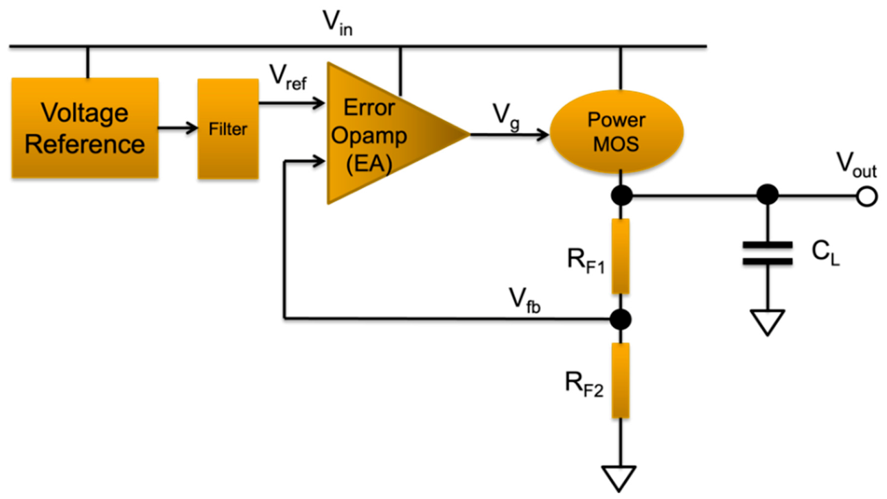
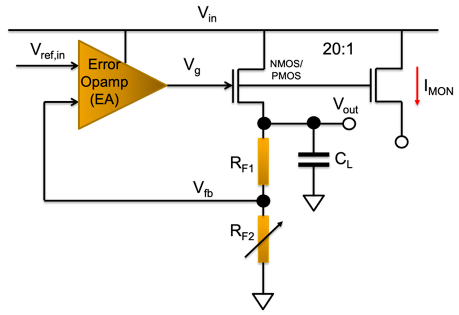
A simplified block diagram of an LDO is shown in
Figure 1. An LDO consists of a power output transistor (NMOS or PMOS, also called a “pass transistor”), which, when placed within a feedback control loop, generates a regulated (stable) voltage Vout and supplies an output current to the load. The control loop is composed of an error amplifier (EA) and a resistive divider, R
F1–R
F2, which, by comparing the generated voltage V
out with the target voltage V
fb (set by the divider), determine the gate drive voltage of the power transistor, V
g.
The output voltage is set by feedback, independently of V
in, according to
The voltage Vref usually is an internal voltage generated by a bandgap reference, thus reducing the temperature dependence of the whole regulator.
LDO regulators are well suited for integration in modern submicron CMOS technologies and can be implemented both as standalone devices and as embedded blocks in complex systems such as microcontrollers used in satellites as housekeeping or for propulsion control, etc. (i.e., SoC). Moreover, the use of standard CMOS processes facilitates portability and scalability across foundries, while radiation-hardening-by-design (RHBD) techniques can be applied to ensure robustness against radiations. Indeed, the space environment requires the employment of radiation-resilient components able to safely operate during the whole system’s life. Thus, besides usual requirements for terrestrial applications, the goal for “space” engineers is to design and manufacture high-performance radiation-tolerant or even radiation-hard LDOs using standard commercial processes of integration that are inexpensive, easy to maintain, and widely available in the industry.
1.2. Radiation Issues
Space ICs are primarily threatened by high-energy radiation such as heavy ions, protons, electrons, X-rays, and gamma rays, which can degrade circuit performance or, in extreme cases, cause permanent damages. Two main classes of effects must be considered: total ionizing dose (TID) and single-event effects (SEEs). TID is a cumulative phenomenon that develops over time. It results from the continuous generation of electron–hole pairs, leaving trapped charges in sensitive parts of the chip, such as shallow trench isolation (STI) and transistor channels. This leads to a gradual shift in threshold voltage—decreasing in NMOS devices and increasing in PMOS devices—which can ultimately compromise correct operation [
3,
4]. This process alters key transistor parameters, such as increased leakage currents, shifts in threshold voltage, and reduced transconductance (g
m). These variations can significantly affect analog circuit performance, as parameters like gain, accuracy, and feedback loop stability strongly depend on transistor transconductance and output resistance.
In contrast, an SEE is a stochastic effect caused by individual high-energy particles striking the device. Heavy ions directly deposit energy along their path, while protons may induce secondary reactions (e.g., generating alpha particles through interactions with materials like boron in passivation layers). These events produce dense electron–hole pair generation, leading to transient currents in transistor channels due to carrier drift and diffusion. At the circuit level, this manifests as voltage spikes known as single-event transients (SETs). When such transients affect memory elements like flip-flops or latches and alter their stored value, the phenomenon is referred to as a single-event upset (SEU). In analog circuits they typically manifest as transient disturbances that decay with the circuit intrinsic time constant and often are defined with the term ASET (analog SET).
While SETs and SEUs are typically classified as soft errors, more severe energy deposition can activate parasitic bipolar structures inherently present in CMOS technologies. This may trigger a latch-up condition, known as single-event latch-up (SEL), which represents a critical hard failure mode in space-grade IC design.
Based on these considerations, the aim of this work was the development of a radiation-hardened LDO in a standard CMOS technology, targeting medium-load currents (up to 20 mA), nominal input voltages in the 3.3 V range, and an output voltage programmable to 1 V, 1.2 V or 1.8 V to accommodate different supply needs of the load. To enable a comprehensive evaluation, two LDO regulators were implemented, featuring NMOS- and PMOS-based output power transistors, respectively. This dual implementation allows for a direct comparison of their electrical performance, as well as an assessment of potential differences in degradation under radiation exposure. Moreover, it provides two alternative LDO solutions suitable for distinct application scenarios, where design requirements and constraints may differ. The LDOs incorporate a trimmable bandgap reference (BGR) to generate the required reference voltage. The reference level can be adjusted through a 4-bit control, providing 16 discrete steps to compensate for output voltage deviations caused by process mismatch, gradients, and intrinsic inaccuracies of integrated components.
So, it is worth pointing out that the main contribution of this work is not the introduction of a new LDO topology, but the radiation-hard implementation and experimental validation of two conventional LDO architectures in a standard 180 nm CMOS process. The simultaneous characterization of NMOS- and PMOS-pass-device implementations under the same technology and radiation conditions provides additional insight into the suitability of the two architectures for deep space applications. Indeed, regarding robustness, it targets deep space performance, i.e., at minimum 1Mrad (Si) total ionizing dose immunity and resiliency to single events. The developed LDO prototypes have been characterized using an improved version of the testing methodology under radiation already used for SRAM [
5], ADC [
6] and DAC [
7].
The following section illustrates state-of-the art and main approaches to implement a rad-hard LDO. Then, the proposed LDO architecture and design countermeasures taken to make it radiation hard are presented. In this section, we discuss the relevant points of the layout style, which also has an impact on ionizing radiation resilience. Finally, in
Section 4, test results both in a lab environment and under radiation are shown.
2. Rad-Hard LDO Voltage Regulators
A search for commercial rad-hard linear regulators led exclusively to standalone devices, i.e., components already assembled in packages and therefore not integrable into more complex systems such as SoCs.
Table 1 summarizes the main results of the search.
Several observations can be made. Most of the listed components are implemented in legacy bipolar technologies, which cannot be integrated into modern systems based on deep submicron CMOS technologies. As a result, they cannot be used as embedded components. This also limits their portability across different silicon foundries. Moreover, as can be seen from the current and voltage columns, they cover only a specific application range, namely high load current applications. Finally, their resilience to TID cannot reach the performance level required by deep space applications.
The LDO proposed in this work aims to address lower load current ranges, as required by power supplies for low-power devices based on modern CMOS technologies. Furthermore, the use of a standard CMOS integration technology makes it flexible enough to be used both as a standalone component and as an embedded macro-block in complex integrated systems. This also facilitates portability across different foundries.
A similar search for rad-hard LDO linear regulators was conducted in the available scientific literature [
8,
9,
10,
11,
12,
13,
14,
15,
16,
17,
18,
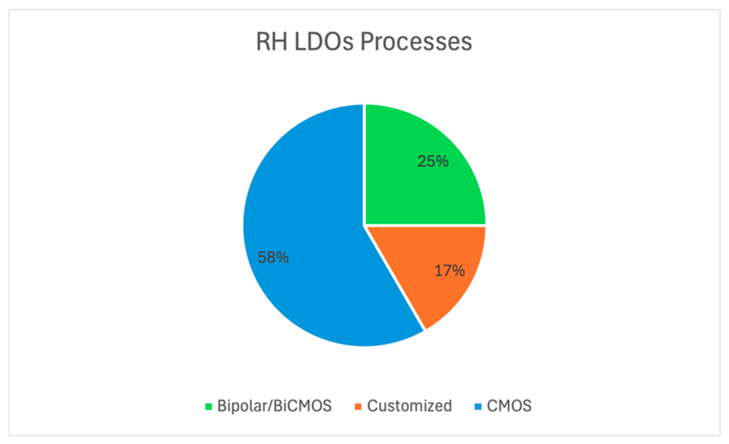
19]. As can be observed, their number is quite limited, and they mostly represent academic proof-of-concept designs. They can be categorized in different ways, for example, by technologies. As can be seen from the cake diagram in
Figure 2, main of them are integrated using CMOS technologies ranging from 250 nm down to 20 nm [
8,
9,
10,
11,
12,
13,
14]. Of the total, 25% of them are bipolar, when a high input voltage must be dealt with [
15,
16,
17]. Finally, special processes are exploited when Radiation-Hardening-By-Process (RHBP) approach is adopted [
18,
19]. Another way to classify them is by power MOS. Nine of them are with a PMOS transistor, while three are with NMOS. The choice between the two depends on the requirements, as will be briefly discussed later in this work. The remaining are PNP.
It should be noted that numerous “terrestrial” state-of-the-art LDO architectures have been recently proposed to improve key performance metrics, such as transient response, stability, power supply rejection ratio, and integration capability. However, the scope of this work is specifically focused on LDO regulators designed for operation in radiation environments, with particular emphasis on radiation-hardening techniques and experimental radiation characterization. Nevertheless, two recent advances in conventional analog and digital LDO design are also acknowledged to provide a broader perspective on the current evolution of LDO architectures [
20,
21].
For example, ref. [
20] presents a 40 nm CMOS analog LDO employing dedicated compensation techniques to achieve high PSRR while maintaining robust stability under large load currents. More recently, digitally controlled LDO architectures have also attracted significant attention. In [
21], a fully synthesizable digital LDO implemented in a 65 nm CMOS achieves fast transient response and reduced steady-state ripple through a dual-loop digital control architecture. These works demonstrate the continued evolution of LDO architectures toward higher bandwidth, improved transient performance, and increased integration density.
On the other side, a larger body of research and scientific publications (including works by RedCat Devices) can be found on the integrated implementation of rad-hard bandgap voltage references [
22], which represent one of the fundamental building blocks of an LDO linear regulator.
2.1. RH LDO in CMOS Technologies in the Literature
CMOS is the most popular technology for the implementation of rad-hard LDO. Starting from the conventional LDO topologies, different techniques have been applied at circuital (mainly) and layout levels to make them resilient to dose. The first choice in the design is on the nature of the power MOS transistor. The pass power element could be an NMOS or a PMOS [
23]. Both topologies have pros and cons. In particular, the NMOS version has a more critical V
g swing (=V
out + V
gs,MOS), especially for the higher output voltage, V
out. This will manifest itself in poorer line regulation performance. The NMOS pass element benefits from a source follower configuration, so the output node is at the source of the transistor, which translates to lower output resistance and improved stability. However, for a standard NMOS LDO, the input voltage V
in must be equal to or greater than the desired output voltage plus the required headroom. Specifically:
where Vth is the threshold voltage of the NMOS transistor and V
dsat,PASS is its overdrive voltage. Because of this, the minimum required input voltage is generally higher than traditional PMOS-based. Sometimes, to exploit the advantages of the NMOS pass device a charge pump is used to pull the gate voltage of the transistor higher; otherwise, the dropout voltage could be too much high. The circuit is larger and more complex, but very low input, output and dropout voltage can be achieved this way. Alternatively, an auxiliary higher bias rail can be used, thus providing the high gate drive.
On the other side, it does not require an external capacitor, CL, and if present it must be lower than 50 pF, a value beyond which the risk of instability increases.
The PMOS version has a less critical V
g swing. This manifests as superior line regulation performance. Indeed, PMOS pass element source voltage is tied to the V
in supply rail of the regulator; thus, the minimum required voltage is given by the minimum drain source voltage V
ds, required for the pass transistor to stay in the saturation region and regulate properly. PMOS dropout voltage is defined by the following equation:
If the input voltage falls below dropout voltage, the pass transistor operates in the linear region, the open-loop gain of the system deteriorates and regulator accuracy decreases. Moreover, as the load current increases, the PMOS pass element gate voltage moves towards ground, so for large output currents, the pass device must be very large or the input voltage Vin of the LDO must be increased.
However, to remain stable, the PMOS LDO requires a load consisting of a series of a small resistance (min 1 ohm) and a capacitance (min 1 uF). These introduce a dominant pole and a zero in the internal loop.
From the radiation point of view, total ionizing dose effects mainly arise from trapped positive charge in the gate oxide and interface states, and they affect power NMOS and PMOS differently:
NMOS: Positive oxide charge lowers the threshold voltage (Vth shifts downward), making the device easier to turn on and increasing off-state leakage. This can eventually lead to higher static power consumption and functional errors.
PMOS: The same positive charge tends to increase the magnitude of the threshold voltage (|Vth| increases, i.e., Vth becomes more negative), making the device harder to turn on and reducing drive current.
In short, NMOS becomes more conductive (higher leakage), while PMOS becomes weaker (reduced drive strength) under TID, so special layout techniques must be applied.
NMOS
The LDOs presented in refs. [
12,
14] make use of an NMOS pass transistor. In [
12], the authors investigate the sensitivity of two 28 nm bulk CMOS linear voltage regulators to single-event transients through both experimental measurements and simulations. The two regulators differ in the architecture of their error amplifiers, the load capacitance of the amplifiers, and the size of the power MOSFETs. Results show that these design parameters significantly influence the amplitude and duration of SETs. A regulator using a simple folded cascode (SFC) amplifier exhibits lower SET amplitudes and shorter transient durations compared with one using a complementary folded cascode structure (CFC). The study also identifies the charging and discharging paths of the power MOSFET gate capacitance as key factors affecting SET behavior, providing useful guidelines for SET-hardened design. No analysis has been done on resiliency to dose or on SEL. As expected, to get low dropout voltage, a charge pump module boosts the 1.8 V input voltage to a 2.35 V voltage supply for the error amplifier (EA). In the EA, the input stage is powered by a 1.8 V supply, and the output stage is powered by the 2.35 V supply.
Ref. [
14] analyzes the mechanisms of single-event transients in a sub-20 nm FinFET-based low-dropout regulator using both SPICE simulations and heavy-ion experiments. The study identifies the EA and BGR as the most sensitive circuit blocks. Experimental and simulation results show strong agreement in SET amplitude and pulse width behavior. Based on these findings, a radiation-hardened LDO architecture employing a comparator, NMOS power transistor and charge pump was proposed, achieving significant reductions in SET pulse amplitude (>90%) and duration (>50%) while maintaining acceptable power consumption and area overhead. These results are achieved by means of an auxiliary circuit that compensate the transient pulse on the output. However, it needs two additional comparators and two additional reference voltages, with power and area penalty.
2.2. PMOS
The work presented in [
8] is a radiation-tolerant low-dropout voltage regulator intended for high-energy physics applications implemented using 0.25 μm standard CMOS technology. The regulator delivers a fixed 2.5 V output voltage, supports output currents up to 300 mA, and achieves a dropout voltage as low as 150 mV with a PMOS power transistor. The design also integrates protection features against overcurrent, overvoltage, and overheating and includes an enable/disable control pin. To obtain the required tolerance to multi-Mrad radiation levels (between 1.7 Mrad up to 20 Mrad), the design systematically adopts radiation-hardened layout techniques. NMOS devices are implemented using enclosed layout transistor (ELT) structures, while guard rings are employed to isolate n+ diffusion regions operating at different potentials [
24]. The achieved results are a negligible variation on the output voltage (10 mV) for 1.7 Mrad dose up to 110 mV degradation for 20 Mrad.
The authors in [
9] propose a PMOS LDO for radiation detector with the novelty of a hybrid compensation strategy, which combines a partially controlled load-tracking approach with an equivalent series resistance (ESR) compensation technique to improve loop stability with up to 150 mA of load current. The LDO regulator has been implemented with a standard 180 nm CMOS process. To eliminate the radiation effects on the LDO regulator, redundancy design for transistors reduces threshold voltage drift. In the meantime, annular transistor and guard ring layout techniques are adopted in the back-end layout to cut off the radiation-induced leakage current path. However, no information about resiliency to dose or single-event effect is given.
The PMOS LDO in [
11] is targeted to be radiation-tolerant to SEL. The protection against loading radiation effects is obtained by a module-level radiation-hardened-by-design technique, namely a latching current limiter (LCL), which detects load current anomalies (i.e., when the load suffers from single-event latch-up). Further, to realize radiation tolerance, particularly to ensure self-robustness against SELs, the LDO is designed with wide guard rings and with deep N-wells. The proposed LDO-cum-LCL is implemented in a commercial 130 nm CMOS process. Performance of integrated samples have been evaluated by means of laser testing. Measurement results demonstrate that the proposed LDO-cum-LCL remains immune to SEL events, even under extended exposure to the maximum laser energy of 4.2 nJ, selected to avoid possible physical damage. No relevant information regarding dose resiliency is provided.
Ref. [
10] shows the behavior of an LDO implemented in a 180 nm CMOS under transient ionizing radiation. The LDO includes a novel TSSS (time-skewed space-split) hardening structure in the power PMOS, which is proved to be effective on mitigating disturbance pulse width of V
out for its recovery. However, only simulation results are provided. Finally, ref. [
13] proposes a radiation-hardened power supply architecture featuring an integrated capacitorless LDO for pixel readout ASICs. A novel hardening structure is introduced to efficiently discharge radiation-induced charges while minimizing area and power overhead. Designed in a 180 nm CMOS process, the architecture achieves highly uniform pixel supply voltages with sub-1 mV variation, low power consumption, and strong radiation tolerance. In the design they do not pay attention to TID, but to SET only. To cope with transients, a novel structure, named Fast Discharge Structure, is introduced. It can quickly discharge the radiation-induced charge at the sensitive nodes. The obtained SET mitigation is demonstrated only with simulations.
2.3. RH LDO in Bipolar Technologies in the Literature
Because of their high current amplification, robust drive strength, and relatively low susceptibility to high-dose-rate radiation and SEL, bipolar transistors can be used in analog circuitry for high-performance space-qualified LDO regulators. Nevertheless, when exposed to low-dose-rate radiation, they can experience enhanced low-dose-rate sensitivity (ELDRS), which reduces their current gain and consequently worsens the performance of bipolar LDOs, causing failures in space electronic systems. Indeed, electronic components used in space are generally subjected to low-dose-rate radiation generated by high-energy particles, typically at levels <1 rad/s (Si). This environment differs significantly from the high-dose-rate conditions (around 50 krad/s (Si)) encountered in high-energy nuclear physics experiments. Furthermore, continuous progress in fabrication technologies has shrunken bipolar transistors as well, which has increased the occurrence of SETs in bipolar LDO devices.
The paper in [
17] presents a bipolar LDO regulator specifically designed to tolerate low-dose-rate radiation in the range of 0.01–0.1 rad/s (Si), representative of the space environment, while providing high load-driving capability, low quiescent current consumption, and high output precision. The techniques adopted include the following:
A new buried LPNP power transistor is introduced to improve resistance to low-dose-rate radiation, while also increasing current gain, reducing quiescent current, and improving the LDO’s transient response.
A distributed driving approach with parasitic resistance-aware VBE matching to achieve balanced current and thermal distribution in multi-cell power transistors, improving both high-power performance and radiation tolerance.
The chip also includes segmented high-order temperature compensation to reduce temperature-induced drift in the LDO’s reference voltage. Apart from the distributed driving approach, the LDO adopts quite a traditional architecture with PNP power MOS, while the novelty is concentrated in the BGR compensation. Overall electrical performance consists of a maximum load current of 7.5 A, input voltage of 2.1 V–30 V and load regulation of 0.3 mV/A. Radiation test results show that the LDO chip can withstand low-dose-rate radiation levels above 300 krad (Si). In addition, the device exhibits strong immunity to both SEL and SETs, achieving tolerance at linear energy transfer (LET) values greater than 99.8 MeV·cm2/mg. The tolerance to low-dose-rate radiation is substantially improved through dedicated radiation-hardening techniques applied at both the circuit design and fabrication levels. However, even if the buried LPNP process is compatible with the standard bipolar process, being customized this technique suffers from higher cost and need of maintenance over time.
Another two LDO implementations make use of a BiCMOS process. Reference [
16] presents a standalone LDO with fast transient response designed for space applications. The regulator supports an input voltage range from 2.8 V to 5.5 V and can deliver up to 6 A of output current. The overall design starts from conventional architecture (
Figure 1); however, it introduces a transient enhancement stage (TES) between the EA and the class AB driver, which reduces the loop delay and improves the transient response speed. The EA, TES and driver have a BiCMOS style topology. The design incorporates radiation-hardening techniques, in a ring gate layout that surrounds only the MOS drain, conventional ELT, and EGR (extended guard ring). Thanks to them, the device achieves a total ionizing dose tolerance exceeding 150 krad (Si) at 6 rad/s (Si), while also demonstrating SEL immunity above 99.8 MeV·cm
2/mg. It features excellent performance through a combination of optimized circuit techniques, packaging solutions, and related design strategies. However, while exhibiting SEL immunity of no less than 99.8 MeV·cm
2/mg, it can withstand a total dose of no more than 150 krad (Si) (at 6 rad/s (Si)), not suitable for deep space. It can be supposed that this dose resiliency limitation could be due to the thick oxide present in this 0.6 um BiCMOS process. Moreover, the novel ring layout could give issues with verification tools.
The work in [
15] presents a radiation-hardened LDO designed to withstand transient ionizing dose rate effects. The hardening strategy combines both circuit-level and device-level techniques. At the circuit level, a dual-feedback loop architecture is introduced to improve the LDO’s response to radiation-induced output voltage disturbances. Implemented in a 0.35 μm BiCMOS process, the authors indicate that the proposed LDO successfully withstands transient gamma radiation dose rates up to 1 × 10
9 Gy/s (Si). However, in the paper, they do not provide enough additional information.
RH LDO in Customized technologies in the literature
Another common way to counteract radiation effects is to exploit a process enhancement (RHBP [
4]). This approach has pros and cons. Regarding the advantages:
High radiation tolerance through process-level hardening techniques.
Intrinsic device robustness since the radiation tolerance is built into the semiconductor structure itself.
Reduced circuit design complexity since fewer redundancy or protection circuits are needed.
Lower sensitivity to parametric degradation.
However, by adopting RHBP, there are some disadvantages:
Higher manufacturing cost because of specialized fabrication processes, additional mask, etc.
Limited access to advanced technology nodes since radiation-hardened processes are often based on older technology nodes.
Reduced performance compared with commercial technologies.
Lower flexibility since designers are constrained by the specific hardened process rules.
Lower yield with respect to standard CMOS.
Smaller commercial ecosystem being supported by fewer foundries and design tools compared with mainstream commercial semiconductor processes.
Despite these limitations, a couple of examples are reported in the literature. A multifunctional radiation-hardened high-voltage (HV) and low-voltage (LV) linear regulator system is proposed in [
18], with a total dose resistance of no less than 7 Mrad (Si). It belongs to a power management solution developed in ASIC for silicon photomultiplier SiPM-based detectors used in high-energy physics experiments. The chip provides adjustable point-of-load linear regulation for the SiPM bias voltage, supporting ranges from 10 V to 70 V with currents up to 50 mA (HV) and from 1.6 V to 3.3 V with output currents up to 800 mA (LV). It also includes features such as SiPM current monitoring, overcurrent protection, and thermal protection. This device is specifically designed for operation in radiation environments typical of particle physics applications, where exposure levels can reach a few Mrad (up to 7) of total ionizing dose and 28.4 MeV*cm
2/mg. While the starting architecture is a conventional one (
Figure 1), with a PMOS power transistor, radiation-hardening strategies include first ring-shape MOS and extended guard ring. The technology (Onsemi I3T80 0.35 μm CMOS) was specifically selected since it provides both low-voltage and high-voltage MOSFETs for the two sections of the regulators, as well as adequate radiation tolerance with respect to the target application. Moreover, I3T80 includes lateral and vertical double-diffused MOSFETs (DMOSFET), which are well suited for high-voltage applications thanks to their drift region structure, which allows for them to withstand large drain-source voltages. Although it is well established that DMOSFETs exhibit an increase in on-resistance due to displacement damage in the drift region, this phenomenon is generally expected to become relevant only at radiation doses exceeding several Mrad [
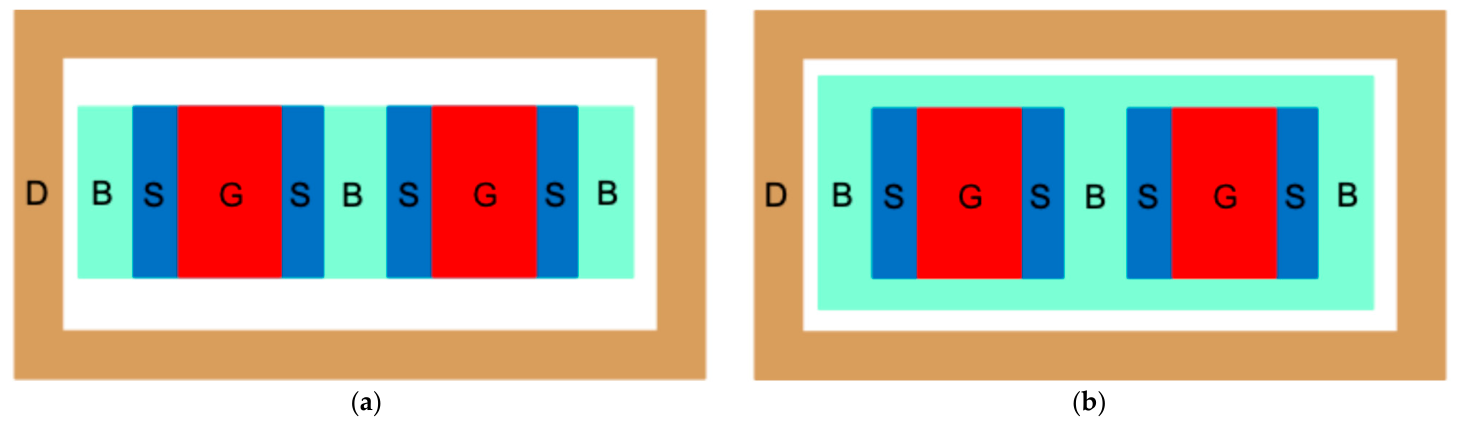
25]. However, the high-voltage n-type vertical DMOSFETs in this paper employ a novel modified layout whose concept is shown in
Figure 3. An extra P+ diffusion region (bulk contact, highlighted in light green) is placed around the device to prevent the thick oxide layers used for spacers and passivation from directly bordering the upper and lower edges of the source region (dark blue). This approach efficiently minimizes drain-to-source leakage currents caused by charge accumulation in the thick oxide under total ionizing dose radiation exposure.
A second implementation with a customized process is shown in [
19]. This paper introduces a 3.5 A low-dropout regulator with unconditional stability. Through optimized loop pole positioning and suitable zero-compensation techniques, the regulator maintains stable operation over a broad range of output capacitances (0–220 μF) and load currents from 0 to 3.5 A. The circuit was implemented in radiation-hardened 180 nm BCD technology and employs several radiation-hardening-by-design methods at both the schematic and layout levels. Based on the conceptual block diagram shown in
Figure 1, the LDO architecture comprises a two-stage error amplifier. As for RHBD, this work makes use of a 0.18 μm BCD process optimized for radiation hardening and developed starting from a commercial platform. A radiation-hardening method for the STI field region was implemented through ion implantation. This approach increases the inversion threshold voltage of the P-type silicon at the STI/substrate interface, effectively preventing the turn-on of parasitic edge transistors and reducing leakage currents along the channel sidewalls. Experimental results on single devices demonstrate that the implementation of the STI field-region radiation-hardening approach considerably improves the radiation robustness of NMOS transistors compared with standard BCD technologies. For this reason, they avoid enclosed-layout MOS. In the paper, experimental results for the LDO demonstrate tolerance to total ionizing doses up to 300 krad (Si), together with SEL immunity at an LET value of 76.5 MeV·cm
2/mg. The regulator provides programmable output voltages between 0.8 V and 3.6 V at the maximum load current of 3.5 A.
Now, the next paragraph will describe the LDOs proposed in this work.
3. 3.3 V Rad-Hard LDOs with 20 mA Load Current
As described above, to develop such resilient components generally, three main approaches have been considered: process enhancement called radiation hardening by process, RHBP [
26], shielded packages and finally design enhancement (radiation hardening by design, RHBD [
27]). While RHBP and shielded packages have been already employed for the development of commercial rad-hard analog components, analog RHBD has not yet extensively applied, and it is mainly confined in the area of high-energy physics experiments [
28].
Starting from a known approach to design LDO regulators, the resiliency to radiation is obtained only by applying RHBD techniques. The target technology for this work is a standard 0.18 μm CMOS whose size allows for compact mixed-signal circuits while guaranteeing good rad-hard performance. The target performances of the prototypes are total dose immunity up to 1 Mrad (Si) and resiliency to latch-up up to 60 MeV*mg/cm2. More scaled and aggressive CMOS processes (such as 90 nm) involve a reduction in gate oxide thickness and seem to be more TID-“tolerant”. However, both SEU (shorter channels and reduced critical charge for SET/SEU) and SEL are expected to be worse.
3.1. Starting Architecture
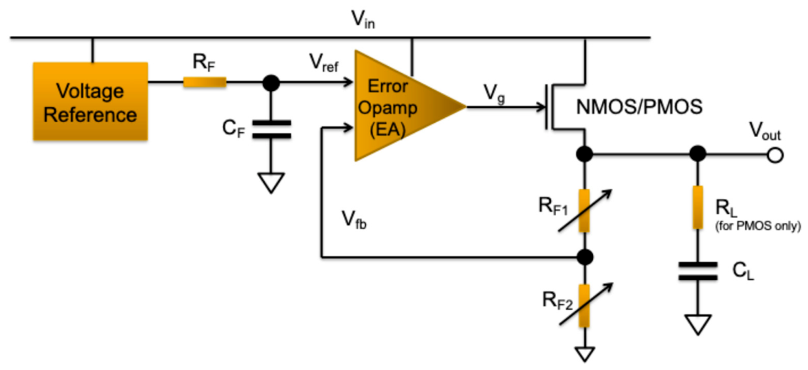
At a high level, the LDO consists of three main building blocks: a voltage reference, an error amplifier, a power transistor acting as the pass element (see
Figure 4) and a programmable voltage divider R
1-R
2. The error amplifier compares a fraction of the output voltage, obtained through the resistive feedback network, with the reference voltage and drives the pass device to maintain (ideally) a regulated output voltage despite variations in supply voltage, load current, process parameters, and temperature. This loop ensures that the output voltage is always at the programmed voltage, modulating the gate potential of the main pass transistor to supply the current required by the load. The precise reference voltage for the error amplifier is supplied by a bandgap reference circuit that has been developed, as well.
As mentioned above, the choice of the pass transistor strongly influences the regulator architecture. In a PMOS LDO, the pass device is connected between the supply and the output node. Since the PMOS gate can be driven directly by the error amplifier, no additional voltage higher than the input supply Vin is required. This simplifies the design and allows for very low quiescent current operation. However, due to the lower carrier mobility of holes, the PMOS device must be relatively large to achieve low dropout voltage and high load current capability, resulting in increased gate capacitance and silicon area.
In contrast, an NMOS LDO exploits the higher electron mobility of NMOS transistors, allowing for a smaller pass device and lower on-resistance for a given area. This generally improves load regulation, transient response, and area efficiency. However, to fully enhance the NMOS pass transistor, its gate voltage must exceed the input supply voltage by approximately one threshold voltage. Consequently, an auxiliary voltage generation circuit, such as a charge pump or bootstrap circuit, is usually required, increasing design complexity and power consumption. In our design, we decided to avoid this complication and accept any potential penalties as a worse dropout. In this work, both NMOS and PMOS pass transistor LDO architectures are investigated. The purpose of considering the two architectures is not to introduce two novel LDO topologies, but rather to evaluate and compare their suitability for radiation-hardened implementations under the same technology and application requirements. The two architectures exhibit only slight topological differences: the pass transistor (NMOS or PMOS), an optimized frequency compensation for the two versions (both at circuit top level and in the error amplifier), and a different power-off mechanism (not shown in the paper).
By implementing and experimentally characterizing both architectures in the same 180 nm CMOS technology, this work provides a direct comparison of their behavior in radiation environments. This approach allows for the impact of the selected radiation-hardening-by-design techniques to be evaluated while minimizing the influence of technology-related differences. The comparison is therefore intended to identify the advantages and limitations of the two architectures for radiation-hard applications, rather than to establish one architecture as universally preferable to the other.
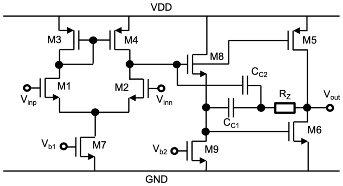
The amplifier must provide sufficient DC gain to achieve the desired output accuracy while maintaining adequate bandwidth to ensure fast transient response. The trade-off between gain, bandwidth, power consumption, and stability is one of the key challenges in LDO design. In our design, the operation amplifier has a two-stages topology, which achieves the class-AB operation in the second stage (
Figure 5). The output of the first stage drives both the NMOS and PMOS of the second stage. The control of the gate of transistor M6 is a shifted-down replica of the input-stage output. Transistor M8 and M9 implement the level shift. Both M5 and M6 contribute to the gain of the second stage; thus, the opamp low-frequency gain will result in being somewhat increased. The compensation network C
C1-R
z achieves compensation (acts to remove the zero in the left plane). However, the 0 degree phase shift provided by the level shift can deteriorate the response, so that the use of C
C2 mitigates the problem.
We have designed two optimized (in compensation size) opamps, one for LDO NMOS and the other for LDO PMOS. The opamps are also equipped with power-off switches (not shown in figure).
3.2. Frequency Compensation Considerations
Although the two regulators employ conventional LDO architectures, their small-signal dynamics and frequency compensation strategies differ because of the different pass device configurations. A simplified discussion of the main poles and zeros is therefore provided below to clarify the stability considerations underlying the two implementations. A detailed analytical derivation of the complete loop transfer function is outside the scope of this work (a useful reference can be found in [
29]), since the novelty of the proposed designs lies primarily in their radiation-hardening approach rather than in the introduction of a new LDO topology.
The stability of the loop is mainly determined by the location of the dominant and non-dominant poles associated with the error amplifier, the pass transistor control node, and, depending on the implementation, the output node.
A. NMOS Pass Transistor Implementation
In the NMOS-based LDO, the pass transistor operates as a source follower, so the pole associated to the output node is at high frequency. The small-signal dynamics are mainly governed by the dominant pole associated with the internally compensated error amplifier and by a non-dominant pole associated with the gate of the large NMOS pass transistor.
The latter can be approximately expressed as
where R
out,EA is the output resistance of the error amplifier output stage and C
g,pass is the equivalent capacitance associated with the gate of the pass transistor, including intrinsic and parasitic contributions.
Because of the large dimensions of the NMOS pass device, the gate capacitance represents a significant capacitive load for the error amplifier and can therefore generate a relevant non-dominant pole. In contrast, as said, the output impedance of the source follower stage is relatively low. The output pole can be approximated as
with R
out approximately equal to the g
m,out. The relatively low output impedance shifts this pole towards high frequencies.
Simulation results confirm that, in the NMOS implementation, the loop dynamics are primarily determined by the error amplifier pole and the pole associated with the pass transistor gate. Therefore, the 100 pF output capacitor is not required as a fundamental compensation component. It was included to evaluate the regulator behavior in the presence of a representative capacitive load.
B. PMOS Pass Transistor Implementation
The PMOS-based LDO exhibits different output node dynamics. In this configuration, the output is connected to the drain of the PMOS pass transistor and is characterized by comparatively higher small-signal impedance. As a consequence, the output pole can occur at significantly lower frequencies, because Rout can be of the order of a few kohm.
For this reason, the output network is explicitly included in the frequency compensation strategy. A relatively large output capacitor is employed to appropriately position the output pole and improve the separation between the dominant and higher-frequency poles. Moreover, a small series resistance R
z is introduced together with the output capacitor, generating a left-half-plane zero approximately located at
where R
z is the small resistor is series to the load capacitance. For the implemented PMOS LDO, the corresponding zero is in the medium-frequency region and compensates, at least partially, for the phase lag introduced by the higher-frequency poles of the regulation loop.
The pole associated with the pass transistor gate can again be approximated by Equation (5). Therefore, the large gate capacitance of the pass transistor, combined with the finite output resistance of the error amplifier output stage, introduces a relevant non-dominant pole. The output zero introduced by the Rz-CL network contributes to improving the phase margin by providing phase lead in the same frequency region. It should be noted that the zero is not intended to exactly cancel a specific pole, but rather to contribute to the overall phase shaping of the regulation loop. In our design, we recommend the use of minimum 1μF with an additional 1 ohm resistor in series for stability.
C. Comparison of Compensation Strategies
The main difference between the two implementations is therefore related to the role of the output network in the overall compensation strategy. In the NMOS implementation, the low output impedance of the source follower pass device shifts the output pole towards high frequencies, and loop stability is mainly determined by the internal compensation of the error amplifier and by the pole associated with the gate of the large pass transistor. Conversely, in the PMOS implementation, the higher output impedance makes the output pole more relevant to the loop dynamics. Consequently, the output capacitor and its series resistance are deliberately exploited to introduce an output pole and a compensating left-half-plane zero.
A qualitative summary of the main frequency domain characteristics is provided in
Table 2.
For LDO PMOS, when the current required by the load changes, so does the output impedance of the regulator, and therefore the output pole can move over several decades in frequency. To ensure stability in all conditions, the error amplifier should have a large bandwidth so as not to introduce poles at low frequency that would degrade the phase margin. This condition is met by our amplifier design, which achieves a bandwidth of about 30–60 MHz, translating to a bandwidth of 25 MHz for open-loop LDO NMOS and 10 MHz for open-loop LDO PMOS.
Due to these different compensation strategies, rather than representing two alternative implementations intended for the same application scenario, the proposed NMOS and PMOS LDOs can be considered complementary solutions. The PMOS implementation is more naturally suited to standalone applications, where an external high-value output capacitor can be exploited as part of the frequency compensation strategy. Conversely, the NMOS implementation is particularly attractive for embedded and fully integrated power management macros, since its stability does not rely on a large external output capacitor.
3.3. Programmability and Calibration
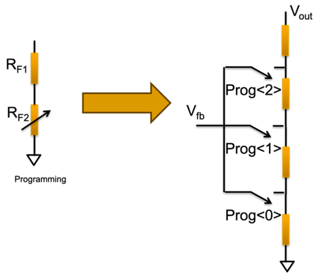
To provide maximum flexibility to multi-voltage operations, we provided the LDOs with programmability, i.e., the possibility to set up three different output voltages: 1 V, 1.2 V and 1.8 V. Naturally, the operation of the NMOS LDO at 1.8 V is penalized by the limited voltage headroom available to properly drive the pass transistor. Programmability is achieved by means of the resistor network in
Figure 6, where Prog<0:2> are the controlling signals for the switches.
Ideally, the output voltage of an LDO regulator is determined by the well-known feedback relationship between the reference voltage and the resistor divider ratio (Equation (2)). Under this assumption, the output voltage depends exclusively on the reference accuracy and the feedback network.
In practice, however, several non-ideal effects introduce deviations from the nominal value. Among the most significant contributors are the input offset voltage of the EA, mismatches in the feedback resistors, finite loop gain, leakage currents and process-induced variations in both active and passive devices. As a result, the actual output voltage may differ from the value predicted by the ideal equation.
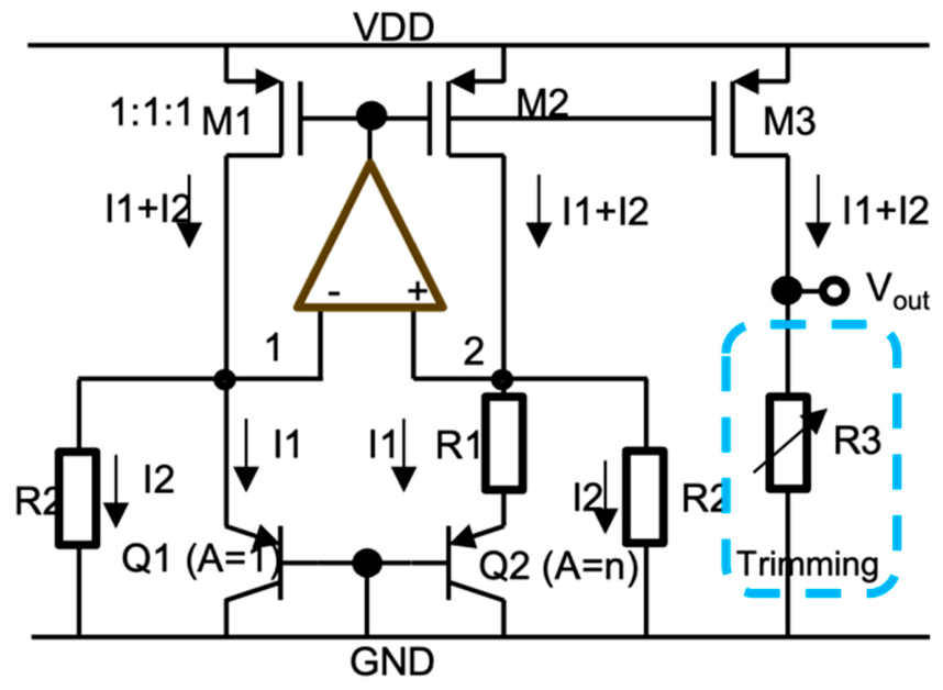
To compensate for these inaccuracies and improve output voltage accuracy, some form of calibration is often required. A common approach consists of trimming the bandgap reference voltage, thereby correcting the dominant error sources and reducing the spread of the regulated output voltage across process corners and manufacturing variations. Such calibration techniques are particularly important in applications requiring high output voltage accuracy and tight regulation specifications. The conceptual schematic of the bandgap reference is illustrated in
Figure 7. The circuit adopts a current-mode architecture [
30] in which a PTAT (proportional-to-absolute-temperature) current is combined with a CTAT (complementary-to-absolute-temperature) current to generate a temperature-independent current of the first order. This current is then forced through an output resistor, R
3, producing the reference voltage V
REF,out.
The core of the BGR is a single-stage folded cascode operational amplifier with an active load. In addition, a dedicated start-up circuit (
Figure 6) ensures the correct initialization of the bandgap reference when the power supply is applied. The output voltage is given by
According to the previous equation, the absolute accuracy of VREF,out mainly depends on resistor matching and on the accuracy of the bipolar transistor area ratio (n). Therefore, process variations introduce an error in the reference voltage, typically amounting up to several millivolts.
To reduce this error and improve the absolute accuracy of the reference, a trimming mechanism can be implemented, as illustrated in
Figure 7. The calibration is performed by adjusting resistor R
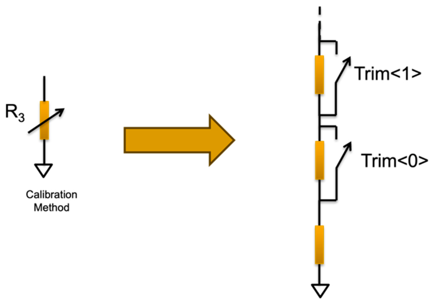
3. Specifically, R
3 is realized as a series connection of binary-weighted unit resistors (R
U), allowing for its value to be finely tuned after fabrication. The number of trimming elements depends on the accuracy requirements of the target application. In the proposed implementation, R
3 consists of a fixed section and a programmable section providing 16 trimming levels controlled by a 4-bit digital word, as shown in
Figure 8. The resulting resistance value can be expressed as
where n = 4. The value of R
FIX has been chosen with Monte Carlo simulations to be in between the inaccuracy interval. The variable part allows for regulation to the correct value. Trimming is activated by means of four external bits (Trim<0:3>).
The voltage range covered by the trim is 190 mV, where minimum step is around 12 mV. A higher bit number would require a greater pin count and more area.
After the BGR, an RC filter has been added, with benefits of forward noise, feedback noise and ASET on BGR. The output of the filter is used as input for the LDO reference.
Both the 4 bits for the calibration of the bandgap and the 3 bits for the programmability of the LDOs can be either set dynamically by the external or stored in a small memory type. This memory is an OTP (one-time programmable) type, based on the anti-fuse principle and demonstrated to be radiation-hardened [
4].
In both LDOs, the additional function of a current monitor, I
MON, has been introduced, which allows for obtaining a reading of the instantaneous current sourced by the LDO (
Figure 9). The output current measurement circuit follows a similar concept by mirroring and attenuating (20:1 ratio). The mirrored output current can be externally converted to a voltage by means of a transimpedance amplifier (TIA) employing a feedback resistor R
F.
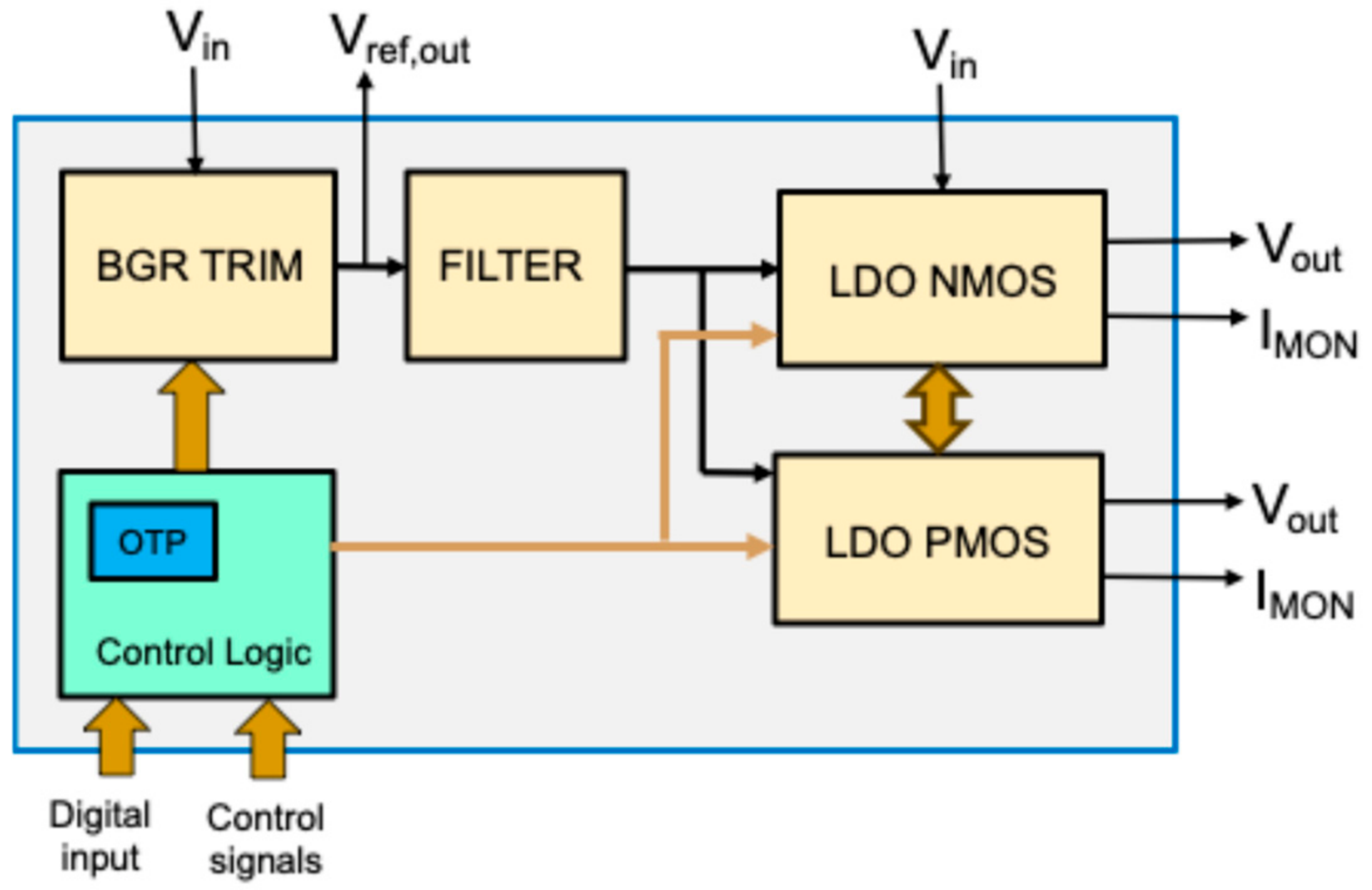
The complete block diagram of the integrated chip is shown in
Figure 10. It includes the two LDOs, a trimmable BGR, its filter, the OTP memory, and the control circuit.
3.4. RHBD Provisions
Layout design was crucial for this application, and due to the fact that the final goal focused on deep space, special care was devoted to shape structures able to go beyond the Mrad (Si) resiliency in TID while still maintaining SELs under control.
There are mainly three blocks where layout design has been critical:
The bandgap reference adopted in this work has been described in a previous work [
22]; here, only the main aspects are reported.
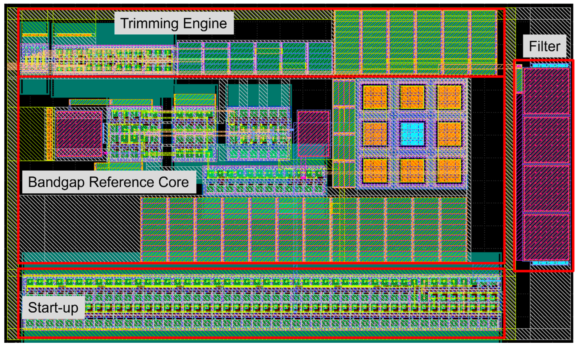
Excluding the output filter using passive elements (a capacitor and a resistor), the core of the bandgap reference consists of a bipolar part where, just like output filter, no particular RHBD has been applied thanks to the intrinsic resiliency of PNP transistors, as well as for poly resistors providing good stability under TID and immunity to SEL, as described in a previous work on rad-hard DACs [
7]; the remaining part, using standard CMOS transistors, has been enhanced using wide ELTs and a common centroid approach in parts where matching has been critical for the good behavior of the bandgap (
Figure 11).
The start-up module (required in every bandgap reference) contains CMOS transistors all shaped without borders (ELTs) to avoid degradation in a high-dose regime. This is not strictly a critical part (it can work even with the threshold slightly shifted), but to avoid any parasitic path with the bandgap reference core, it has been treated with the same RHBD technique used for the rest of the module.
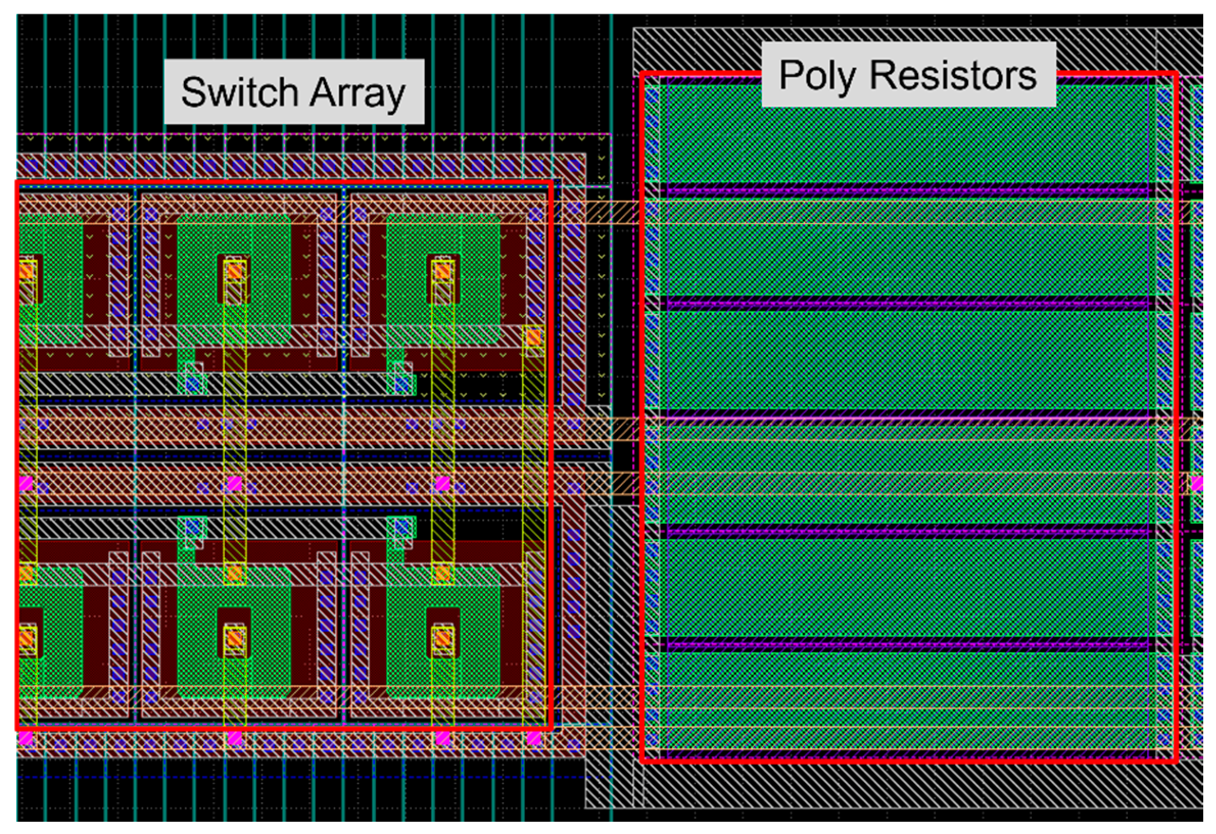
Regarding the trimming engine and considering the high linearity of poly resistors, the main focus has been on switches providing the trimming code for the bandgap; in this case, ELTs surrounded by guard rings to avoid latch-up effects have been designed to guarantee a safe connection between poly resistors, avoiding leakage due to the transistor channels’ border (see
Figure 12).
Radiation-hardening measures adopted in the error amplifier mainly rely on layout-level techniques. In addition, a sufficiently high open-loop gain was targeted to preserve adequate performance margins after radiation-induced degradation. All transistors in the buffer stage were properly sized according to radiation effects reported in the literature, avoiding minimum geometries and employing ELT structures, particularly effective and suitable for deep space.
The offset voltage of the operational amplifier is primarily determined by the matching of the input differential pair and directly affects the EA characteristic. Since radiation-induced threshold voltage shifts do not significantly impact transistor mismatch [
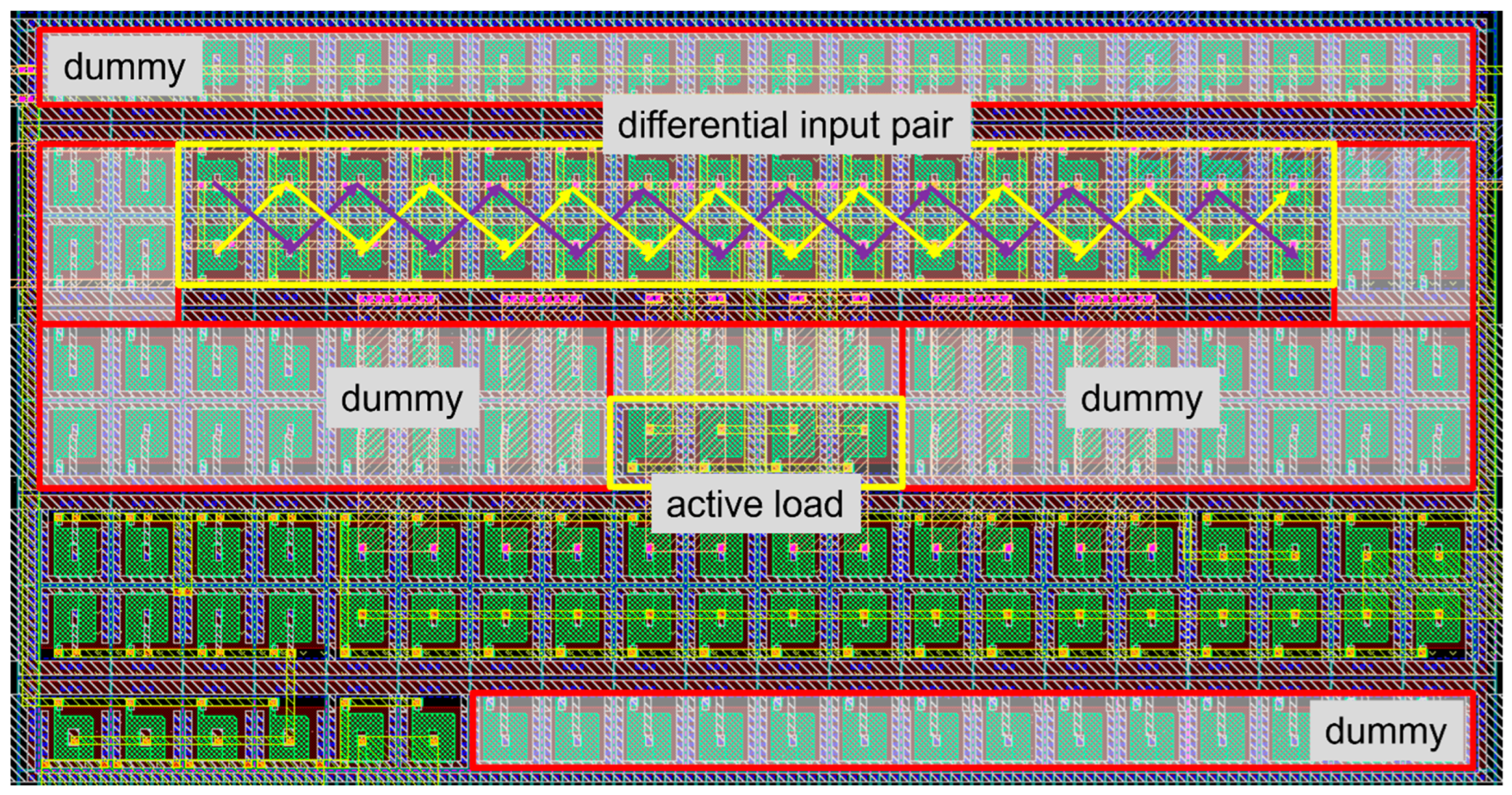
31], particular attention was devoted to the physical matching of the input devices. To this end, a common-centroid arrangement of ELT transistors was adopted (to emulate stacked transistor). The same layout strategy was applied to the active-load and bias circuitry. To obtain a good matching dummy ELTs are placed to mitigate process deviation (error amplifier section),
Figure 13.
The common centroid approach is basically a replication of what is usually done with stacked transistors when design-matched layouts are required (e.g., current mirrors, differential stages); since regular stacks cannot be used because they still keep unprotected borders and considering that ELTs are independent entities that are impossible to stack on each other, the approach is to use more ELTs and place them following a specific pattern.
Figure 13 shows a PMOS differential input pair split in 16 PMOSs for the first input and 16 for the second input; to reduce mismatches, two rows of PMOSs flipped along the Y axis are connected according to the yellow and violet lines, thus obtaining a sort of stack that of course cannot guarantee the same matching of a standard-shaped stack but then indeed does not suffer from border degradation. Moreover, outside the differential pair region, there are dummy transistors to avoid both parasitic paths coming from the TID and providing another level of matching since every ELT “sees” another ELT shaped in the same way on all sides.
The approach adopted in
Figure 13 (and in all other parts of the of the layout) recalls a standard cell approach; in fact, the main module is represented by an elementary cell containing both the P-channel and N-channel version of the elementary ELT transistors; between them, a double guard ring biasing N-well region and P-substrate region guarantees that no latch-up effects can occur for energy release from charged particles (e.g., heavy ions), and an additional ring around the ELT gate further protects against parasitic paths in case of doses exceeding the Mrad (Si) regime.
Apart from the RHBD layout design, this analog standard cell follows the most common rules of Place and Route approach (flipping along axis, grid for routing, etc.).
Figure 14 shows the main cell that, in its naked version, does not have a connection at the routing level or powering connection level; on the right side of the figure shows an example of four of these cells placed, routed, and some connected to become dummy ELTs (dummified transistors).
The final, and maybe the most important, RHBD design has been implemented on the output pass transistors (NMOS and PMOS).
In this case, being a power transistor with a large width able to drive up to 20 mA, ELT is highly recommended, but using the standard cell approach risks losing efficacy.
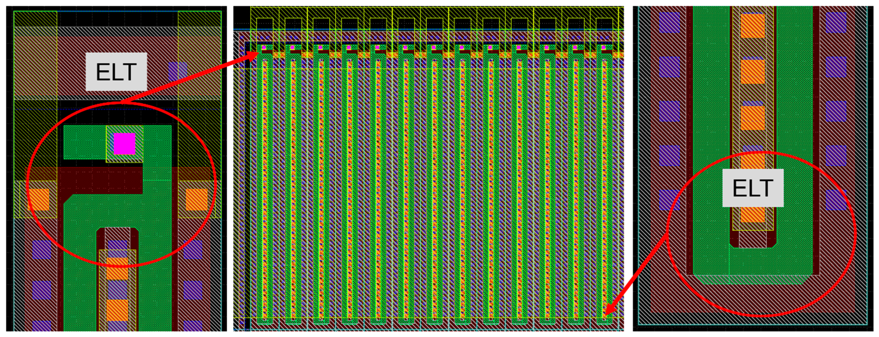
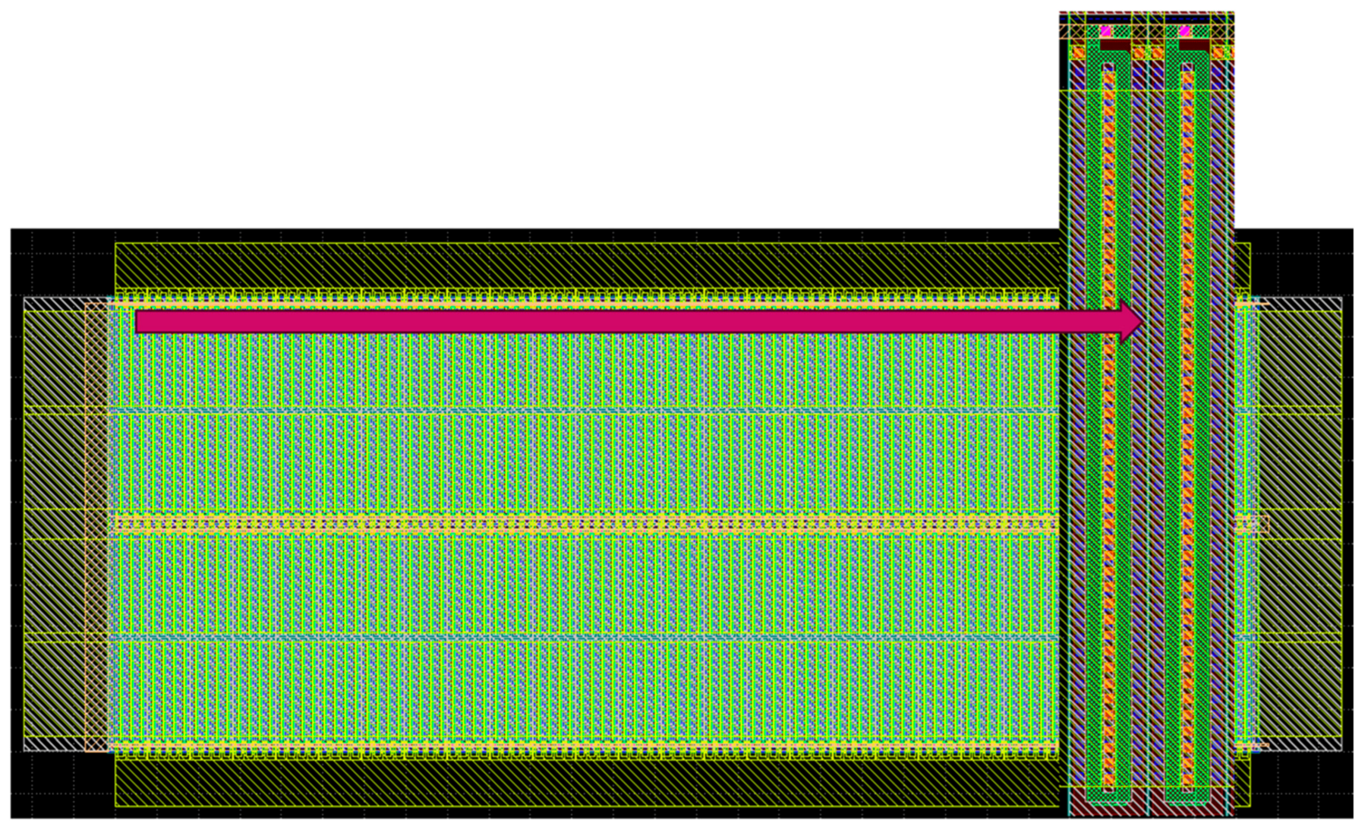
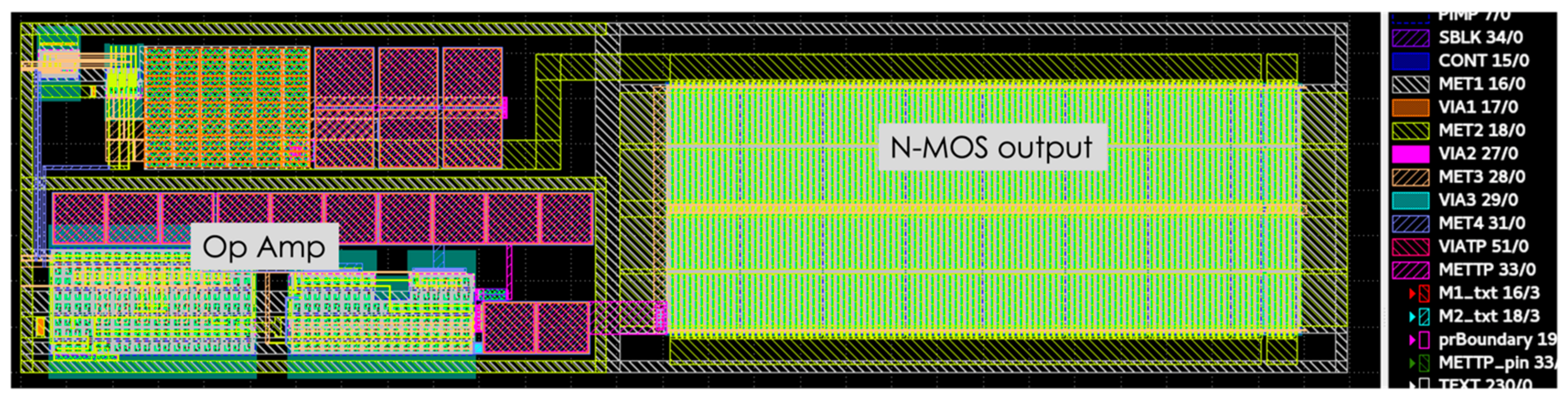
In order to guarantee good matching following the canonical stacking approach, we designed a new structure called “organ pipe” where the ELT is extremely stretched (up to 24 u) and using the minimum distance allowed by the technology along the X-axis, as shown in
Figure 15; in this way a major part of the transistor is like a stack and the ELT parts (those avoiding the borders) are left on the top and on the bottom of the pipe.
The single pipe is 50 u in width with a length that can be very low but that, as a precaution, we fixed at 0.4 u and not at the minimum offered by the technology on 3.3 Volt (0.3 u).
The complete output pass transistor is finally built using an array of ELT NMOS (or PMOS) transistors to guarantee up to 20 mA current load with the layout in an “organ pipe” style (
Figure 16).
For the small digital control section, a proven radiation-hardened library has been used. The library, previously characterized in similar technologies, demonstrated tolerance up to 300 krad (Si) TID, 10 MeV·cm2/mg SEU, and 60 MeV·cm2/mg SEL.
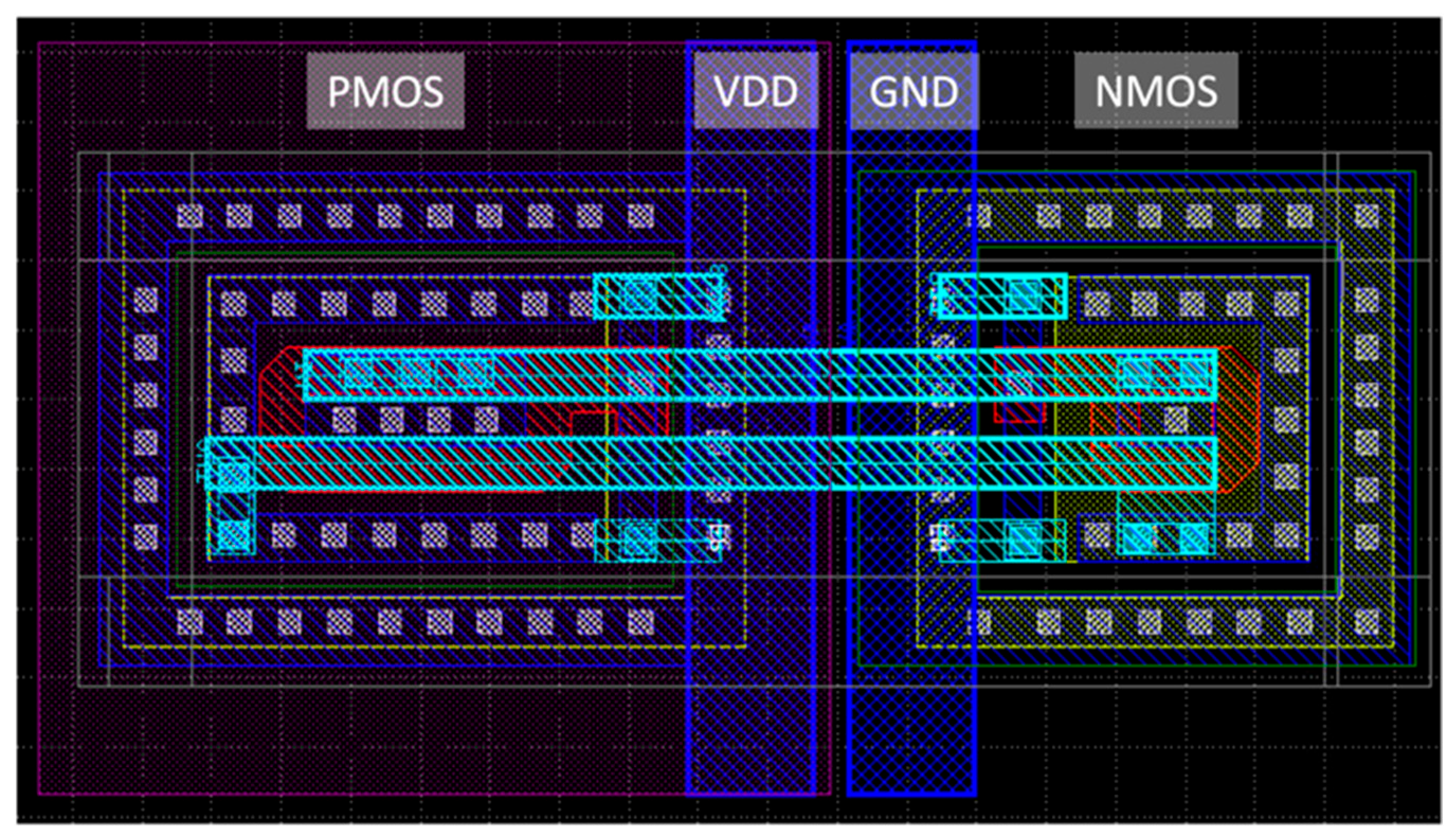
At the layout level, extended guard rings, including multiple N+, P+, and N-well rings, were inserted wherever possible to suppress latch-up mechanisms. Furthermore, all MOS switches employed in the programmable part were implemented using ELT geometries to minimize TID-induced leakage currents. An example is shown in
Figure 17, where the annular gate structure reduces intra-device leakage, while the surrounding VDD and GND guard rings mitigate inter-device leakage and provide additional protection against single-event latch-up.
The LDO layout is shown in
Figure 18 with different blocks identified by labels.
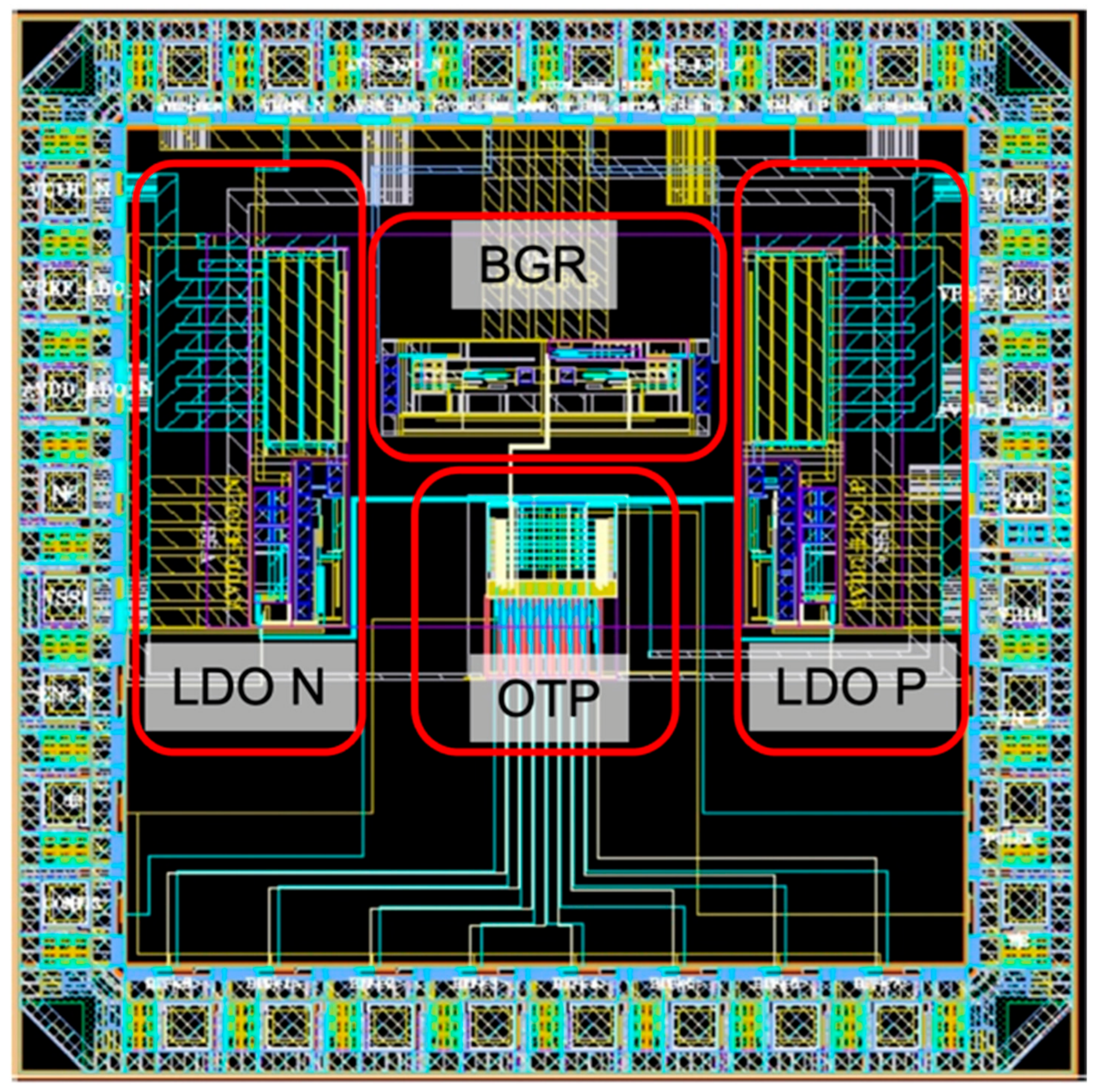
Finally, the layout of the whole test chip is shown in
Figure 19. Its area is 1.6 mm × 1.6 mm (2.56 mm
2) including the padframe.
4. Test Results
The LDOs and the BGR have been integrated in a standard 3.3 V 180 nm CMOS process (XFab XH018).
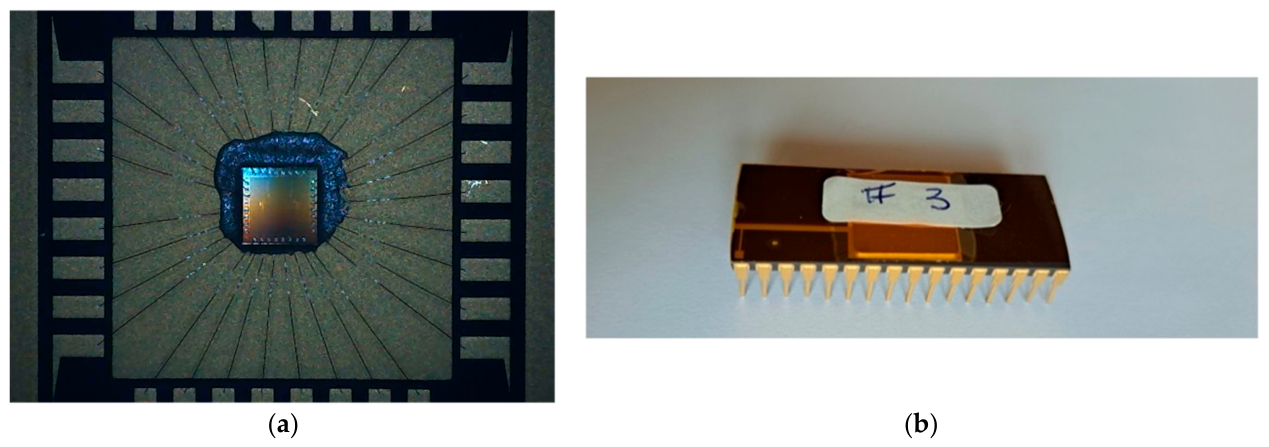
Figure 20 shows the micro-photo (a) and the assembled component (b) in a 32-pin CERDIP. The overall chip area is 1.6 mm × 1.6 mm (2.56 mm
2) including padframe.
In-lab measurements
The prototypes have been preliminary characterized in a lab environment both in terms of static performance, namely absolute output voltage value, trimming and programming capability, line regulation, load regulation and power consumption. In addition, the dropout voltage has been evaluated according to the following definition:
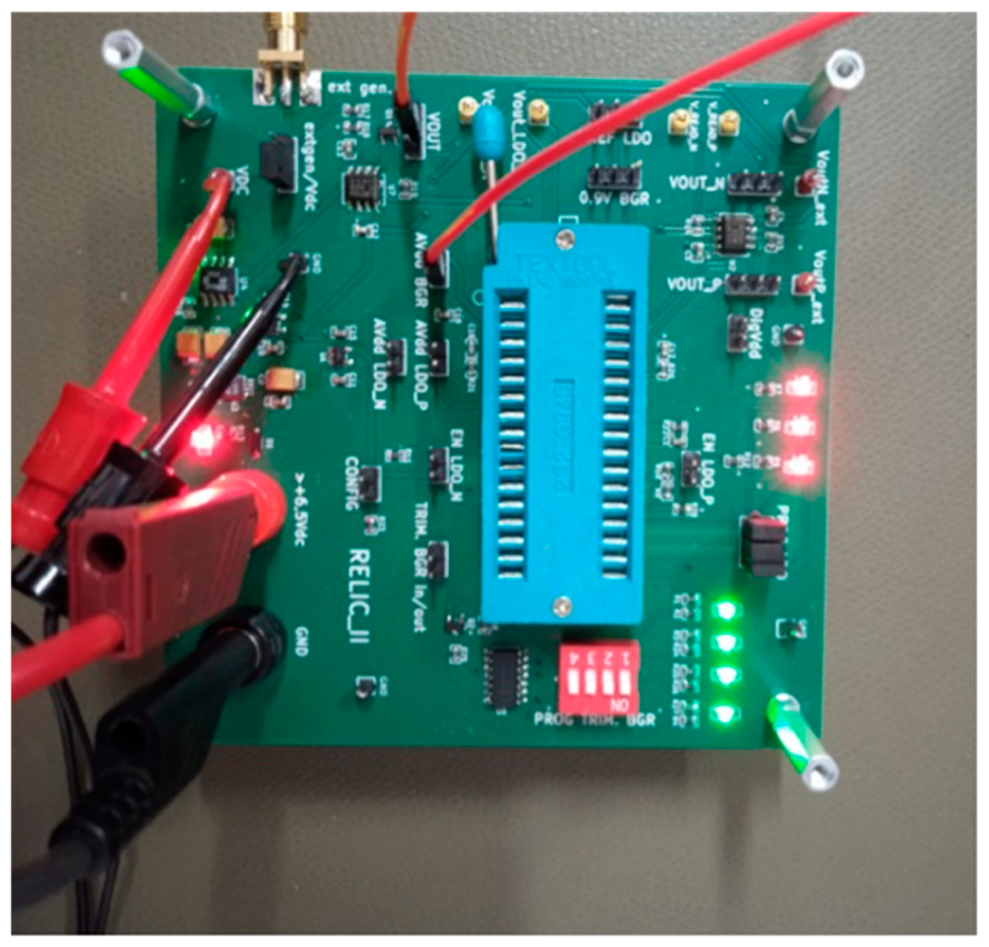
For electrical characterization, a compact test board was developed to provide access to all input and output signals and to facilitate device trimming (
Figure 21). The visible LEDs help to identify if “0” or “1” logic signals have been set for trimming and programming.
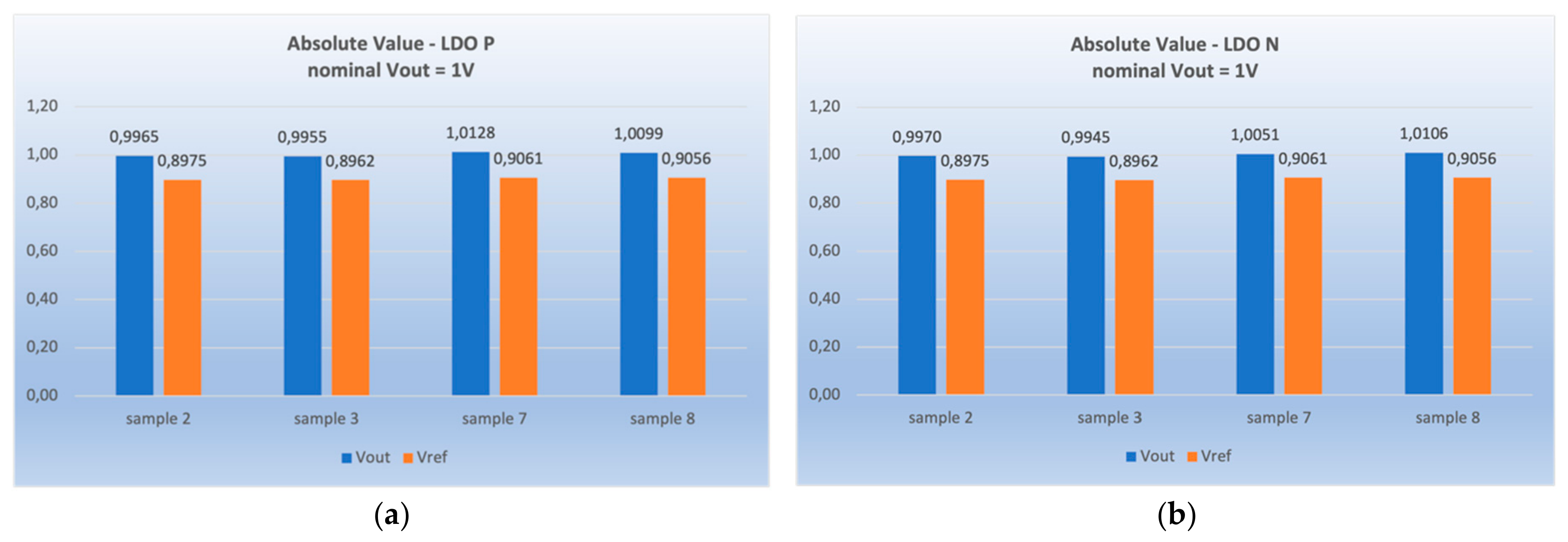
Figure 22a,b show the measured output voltages on four samples for the two LDOs when the trimmable output of the BGR has been adjusted to the value nearest to the nominal 0.9 V (the BGR output voltage is used as reference voltage for the LDOs). Only the 1 V case is shown. The orange bars are the reference voltages generated by the bandgap, while the blue bars are the LDO output voltages.
The max spread due to inaccuracies of the LDOs output voltage is <1.3% (PMOS) and <1.1% (NMOS), respectively. When LDOs are programmed to generate 1.2 V the spread is quite similar (1.6% and 1.5%), while for 1.8 V is a bit larger (3% for both).
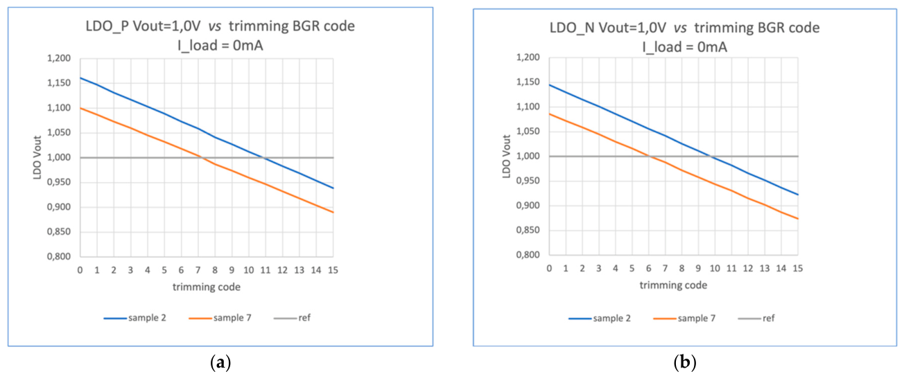
Figure 23 shows the BGR output voltage and the LDO output voltage (for the 1 V) as a function of the sixteen codes of the trimming (from 0000 to 1111). Over 20 samples, 19 of them intercept the nominal output voltage. Same behavior has been observed when the LDOs are programmed for 1.2 V and 1.8 V.
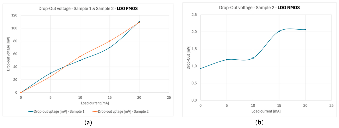
Finally, the drop-out voltage has been evaluated (
Figure 24). As expected, due to the intrinsic topological characteristics, the LDO with PMOS performs better than the NMOS. Indeed, the higher dropout voltage of the NMOS implementation is mainly related to the gate drive requirement of the NMOS pass transistor. Unlike the PMOS implementation, the NMOS pass device requires a gate voltage higher than the regulated output voltage to maintain sufficient overdrive and achieve the required load current capability. This requirement introduces an additional voltage headroom constraint and limits the achievable dropout performance under the adopted operating conditions. Therefore, although the NMOS implementation shares the same general regulation function and was developed for the comparative investigation presented in this work, its measured dropout voltage is significantly higher than that of the PMOS counterpart.
Line and load regulation measurements are defined as follows:
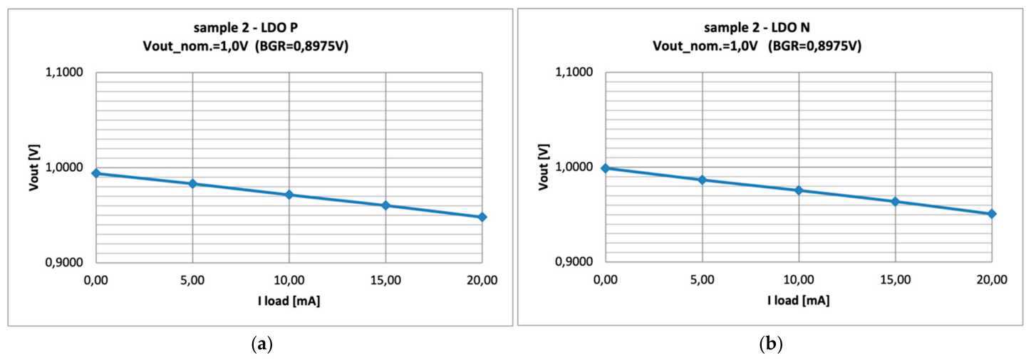
Line regulation: variation in Vout for an input voltage range from 2.1 V to 3.6 V (NMOS) and 1.9 V to 3.6 V (PMOS), with the output current fixed at 20 mA.
Load regulation: variation in Vout for output currents ranging from 0 to 20 mA, with the output voltage set to 1.8 V, 1.2 V and 1 V.
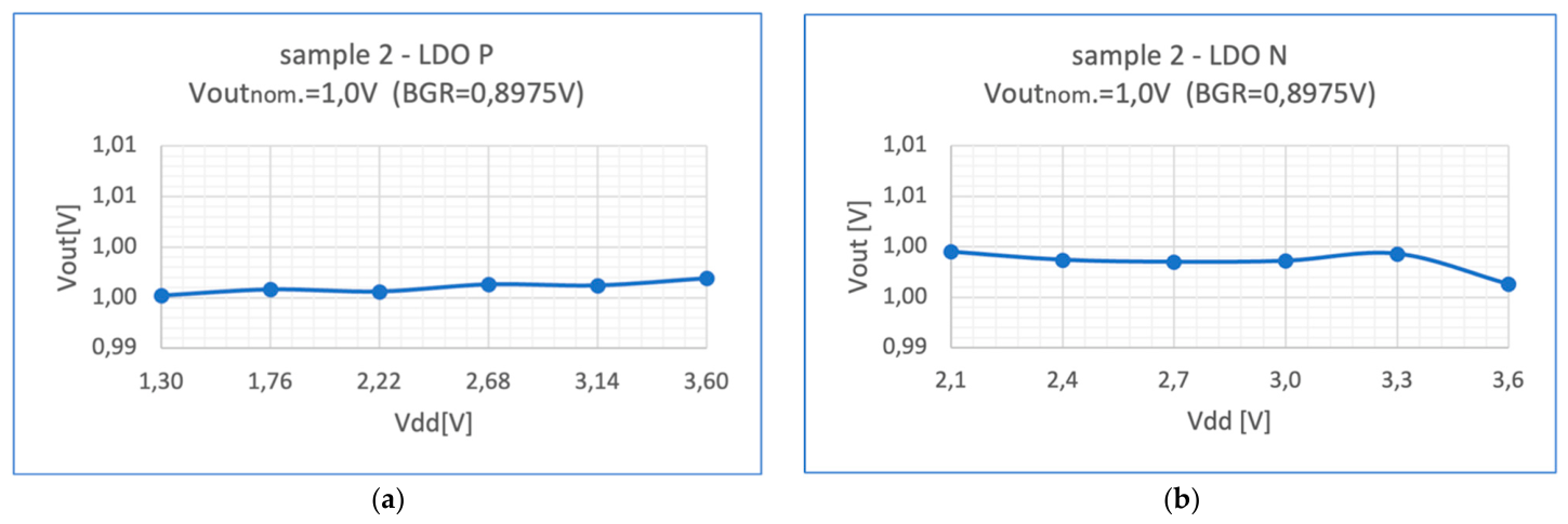
Figure 25 shows the line transient of LDO PMOS (a) and NMOS (b) when the output voltage is set to 1 V.
At 1 V output, the variations in Vout are 1.5 mV and −3.2 mV for PMOS and NMOS, respectively. The variation changes to 3.9 mV and −1 mV for 1.2 V output, and to 4 mV and −1.7 mV for 1.8 V output.
Figure 26 shows the measured load transient for LDO PMOS (a) and LDO NMOS (b) when the output voltage is set at 1 V.
At 1 V output, the variations in V
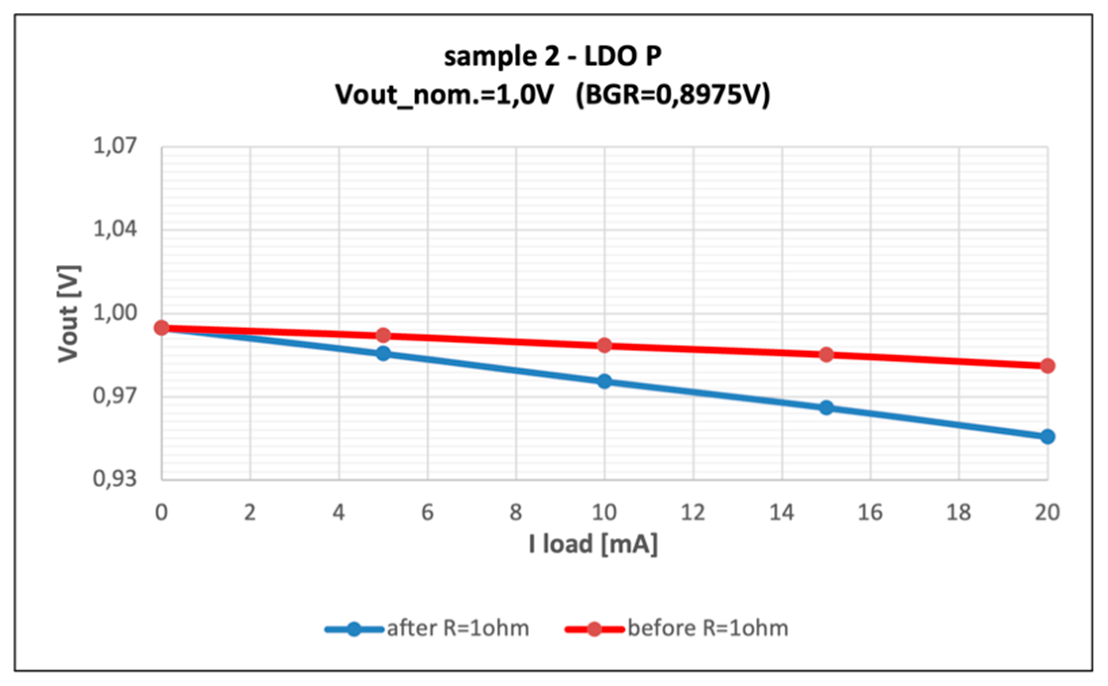
out are 46 mV and 48 mV for PMOS and NMOS, respectively. The variations for 1.2 V and 1.8 V outputs are similar. The observed voltage drop is the result of two distinct contributions: the intrinsic load regulation of the regulator and the voltage drop across the parasitic resistance associated with the layout metal interconnects and the bonding wires. An estimate of the parasitic series resistance, R
par, associated with the on-chip output metal routing, bond wires, and external interconnections gave us a value of more than 1.5 ohm. The corresponding voltage drop was estimated according to
The estimated drop has been subtracted from the measured load regulation variation in order to evaluate, to the extent possible from the available test configuration, the intrinsic regulator contribution. As an example,
Figure 27 shows the measured load transient for LDO PMOS (blue) and the evaluated intrinsic load transient (red), obtained by subtraction of the voltage drop DV
par. Thus, the real drop is lower than 16 mV.
The measured current consumptions for sample 2 are reported in
Table 3. The differences in power consumption as measured on ten samples are negligible. The signal Enable allows for switch off the LDO. On the contrary, the BGR is always ON.
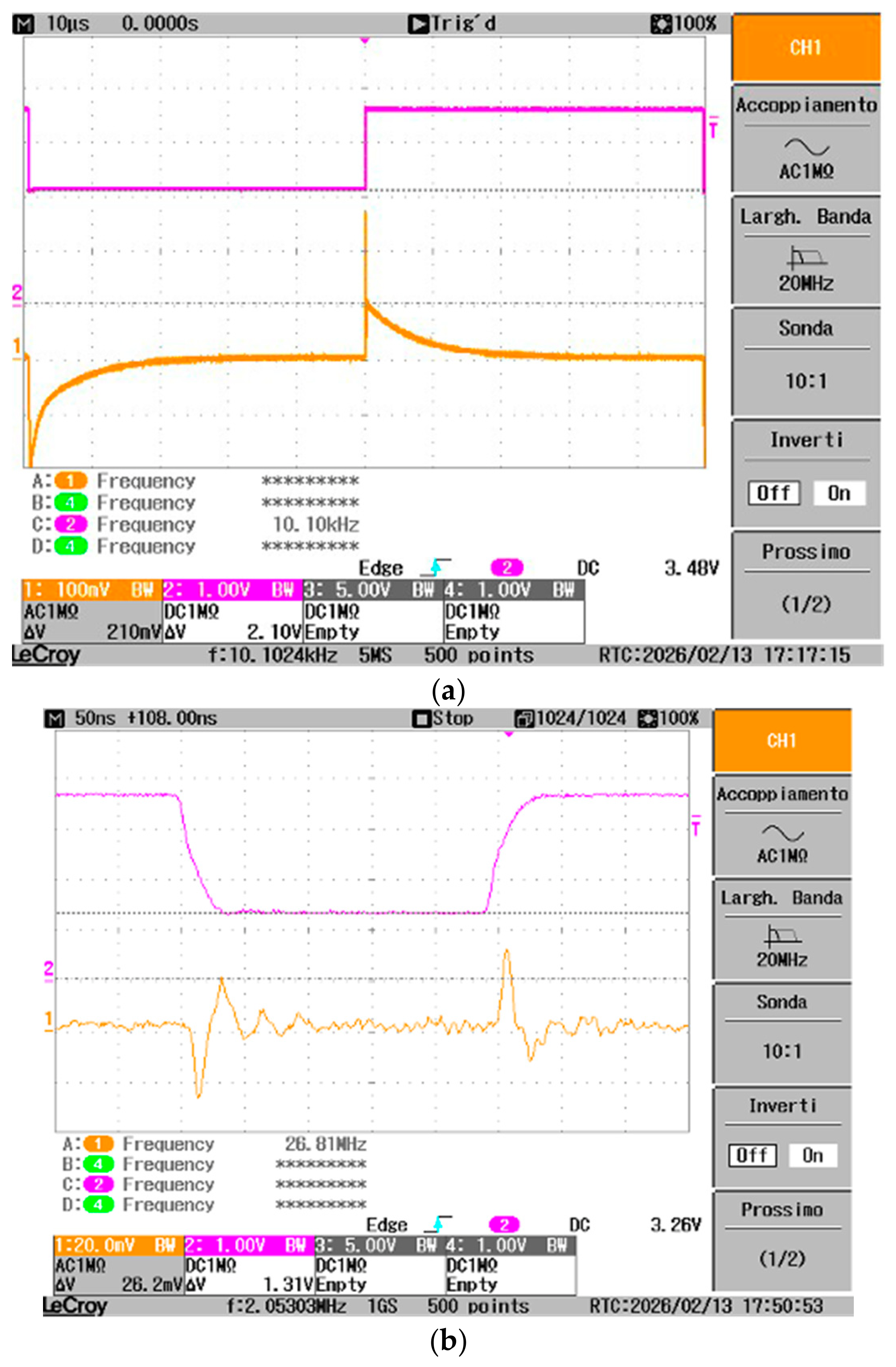
As for dynamic characterization, the measurements concerned the line transient (i.e., how fast the output reacts to a sudden change in the input voltage) and the load transient (i.e., how fast the output reacts to a sudden change in the current load).
Figure 28a shows the measured line transient behavior of the LDO NMOS for 1 V output voltage (orange line). The applied V
in varies from 2.1 V to 3.6 V with a falling edge time and rising edge time of around 200 ns (10% to 90%).
Figure 28b shows the measured line transient behavior of the LDO P for 1 V output voltage (orange line). The applied V
in varies from 1.3 V to 3.6 V with a falling edge time and rising edge time of around 200 ns (10% to 90%).
The rise–fall time of the LDO NMOS is 15 us, while that one of the PMOS is 50 ns. All samples are characterized by the same trend during the falling and rising edge of Vin transient.
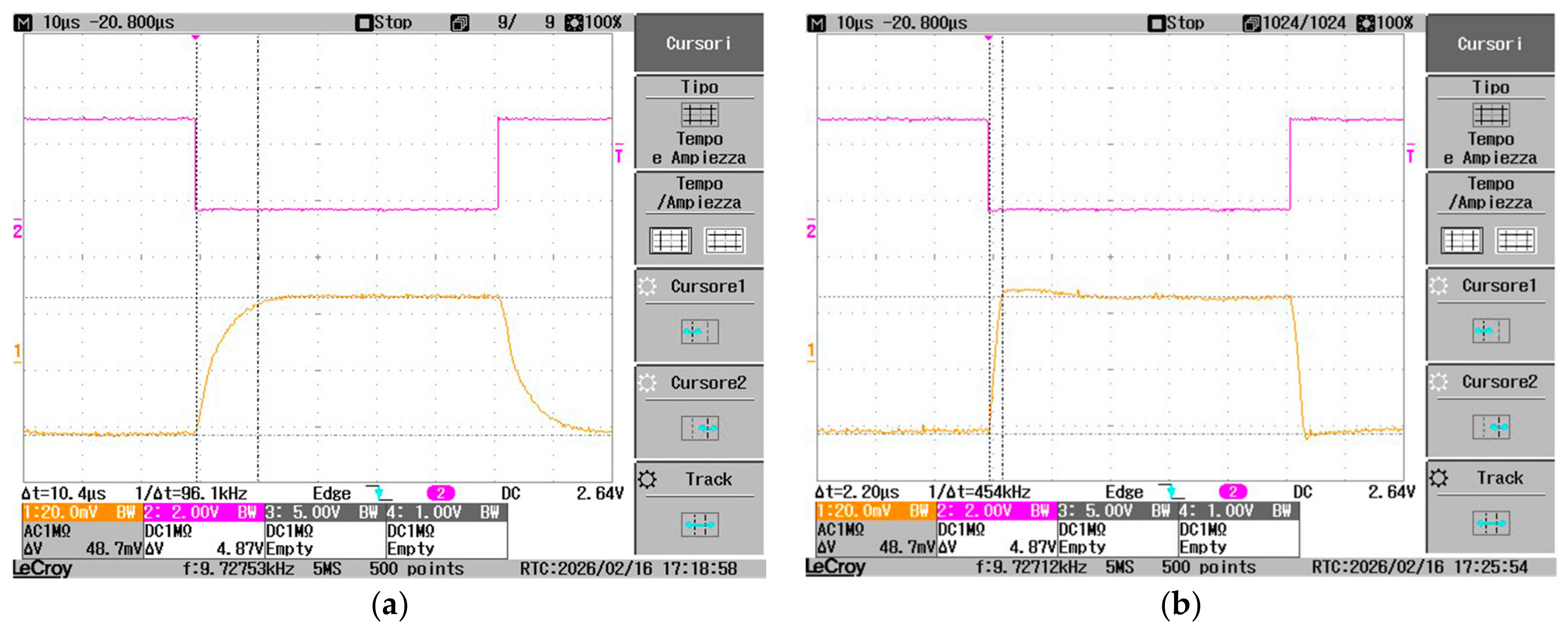
Figure 29 shows the measured load transient behavior of the LDO NMOS (a) and LDO PMOS (b) for 1 V output voltage. The applied I
Load varies from 20 mA to 0 mA. The pink curve is the command to the circuit that activates the current sink.
The LDO output voltage varies of <50 mV, which is mainly due to the output parasitic resistance. The transient speed is in the order of 10 us (NMOS) to 20 us (PMOS). The behavior is the same for all three output voltage values of the LDOs.
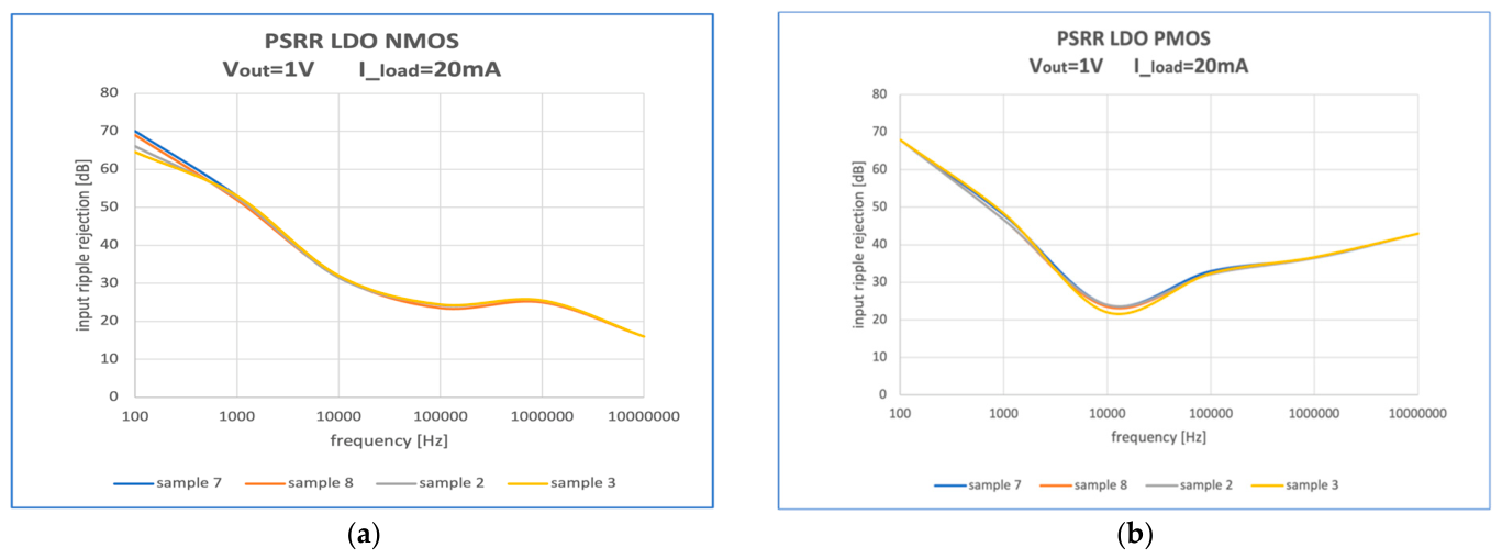
Also, the PSRR was evaluated (
Figure 30) by sweeping a small sinewave at the input of the LDOs and recording the gain at V
out. The measured PSRR is also influenced by the characteristics of the external circuitry, namely the line and load capacitances.
A rejection >50 dB at 1 kHz and >30 dB at 10 kHz is achieved for LDO NMOS, while PSSR is 48 dB at 1 kHz and 22 dB at 10 kHz for LDO PMOS.
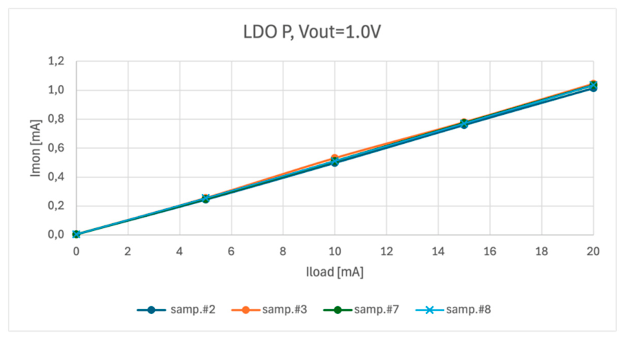
Finally, we measured the current monitor.
Figure 31 shows the result on LDO PMOS, as obtained by connecting a transimpedance amplifier (a current to voltage converter), almost exclusively implemented with one operational amplifier plus a resistance, to the monitor pin.
The measured current corresponds to one-twentieth of the output current supplied by the P-LDO, with a maximum accuracy error of 5%.
The bandgap reference measurements are not reported here in detail, as they have already been mainly presented in ref. [
22]. We can recall that without calibration the spread in the reference voltage is >100 mV. However, thanks to the calibration, the accuracy achievable at room temperature on the 0.9 V is <1% as measured over 20 samples. The TC over 20–90 °C is <200 ppm/deg (with only the first order being compensated).
Measurements under radiation
The test chip was tested under Cobalt 60 irradiation at the IGS-3 (Irradiatore Gamma Sicilia-3”) gamma irradiation facility at the University of Palermo: cell type panoramic irradiator with irradiation cavity, multiple source and variable dose rate [
32]. The facility was fully equipped with the instrumentation for the dosimetry to ensure safe operation and radiation levels according to international standard ESCC No. 22900 [
33].
In radiation testing, the device under test (DUT) is typically radiation-hardened, whereas the associated control electronics are often commercial or only radiation-tolerant. This may lead to failures in the test setup itself, making it difficult to determine whether observed errors originate from the DUT or from the measurement system. Consequently, dedicated irradiation methodologies and test facilities are required to accurately reproduce the radiation environment and operating conditions experienced by electronic devices. Since no general purpose solution is currently available, several customized approaches have been developed for the characterization of analog and digital components [
34,
35,
36]. Most of these methods perform measurements several hours after irradiation, thus failing to capture the device response in real time. The approach proposed by the authors enables real-time monitoring of the key performance parameters, with some compromise in measurement accuracy, and encompasses the entire test ecosystem, including hardware, software, facility, and operating procedures. This methodology typically concerns the TID test. In contrast, SEE and SEL testing with heavy ions is generally less challenging, since the highly collimated ion beam has limited impact on the control electronics.
We used the two-board concept and RedCat Devices’ proprietary Leonida Platform, which includes the overall software environment. Using a 0.8 rad/s dose rate, during the experiment the LDOs (and BGRs) reached > 1 Mrad (Si) with no significant degradation in terms of electrical performance.
The proposed solution involves splitting the test board into two parts [
22]:
A motherboard (MB), which hosts the signal generation, data acquisition system, and auxiliary circuitry;
A daughterboard (DB), carrying only the test chip.
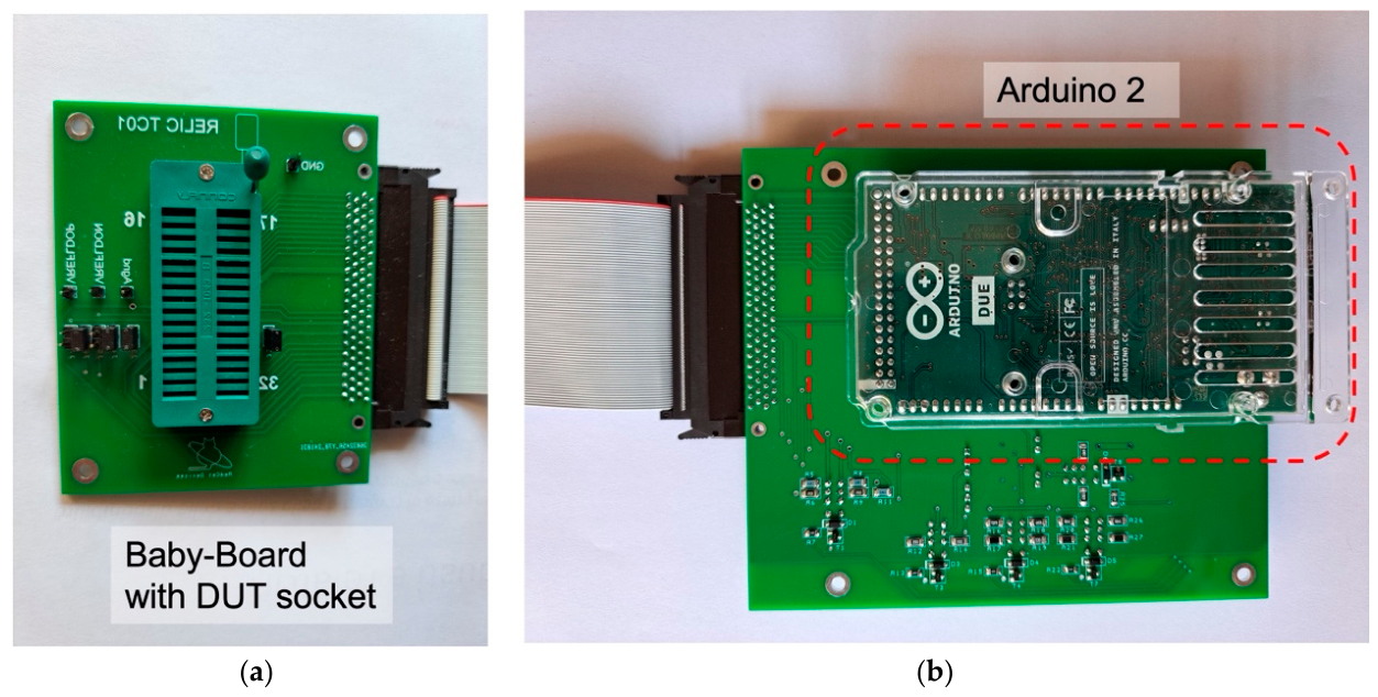
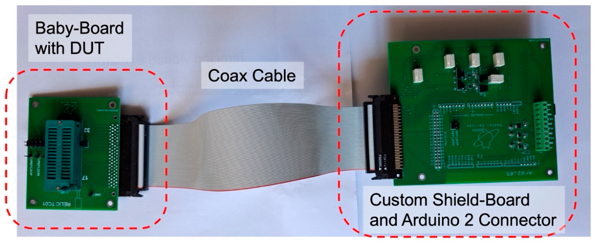
The daughterboard, which hosts the DUT socket, is connected to the motherboard, containing the control electronics, through a flat cable carrying digital and low-frequency analog signals. The DB is shown in
Figure 32a. For the motherboard, an off-the-shelf Arduino Due
® (Arduino S.r.l., Monza, Italy [
37]) was adopted. To enhance its capabilities, a custom shield board was developed and mounted directly on the Arduino Due
®, as shown in
Figure 32b.
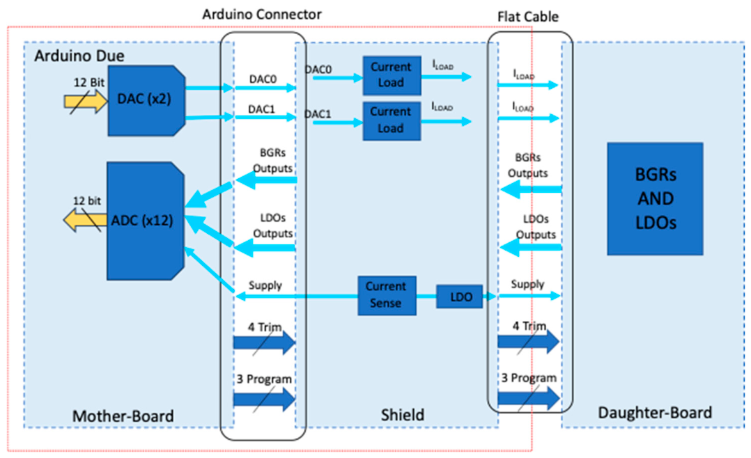
The Arduino Due® provides twelve onboard ADC channels for acquiring analog signals from the DUT (six dedicated to BGR characterization) and two DAC outputs for generating auxiliary voltages. It also supplies the required power rails and generates the digital trim signals for BGR testing. Two additional ADC channels are used to monitor the analog and digital current-sensing outputs through external sensing resistors. Besides the current-monitoring circuitry, the custom shield integrates auxiliary circuits required for LDO characterization.
Figure 33 presents the detailed block diagram of the three boards used in the radiation test setup, while
Figure 34 shows a photograph of the complete system.
As illustrated in this setup, a flat cable is used to carry both digital and analog signals. Coaxial cables are unnecessary since these signals are essentially static.
For TID testing, inside the irradiation facility, we can distinguish two main areas: an area with direct exposure to radioactive sources (Hot Chamber) and a shielded area from radioactive sources (Warm Chamber). The Hot Chamber contains Cobalt 60 rods that can be extracted from the tank from outside the bunker (Cold Chamber) via electromechanical control; the Warm Chamber is protected by a concrete wall and has mechanical manipulators to be used for moving samples (not used in our test). In the Warm Chamber, radiation levels are very low but operators cannot stay during rod extraction from the tank.
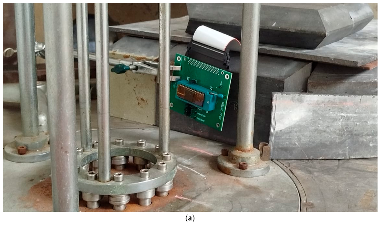
In our case, the component under test (DB) was exposed in the Hot Chamber at the appropriate distance to cobalt rods in order to receive the required dose rate and control electronics (MB) protected in a lead sarcophagus; MB and DB connection (as explained above) was guaranteed by the flat cable running from the sarcophagus to the exposure point (less than 15 cm), as shown in
Figure 35a.
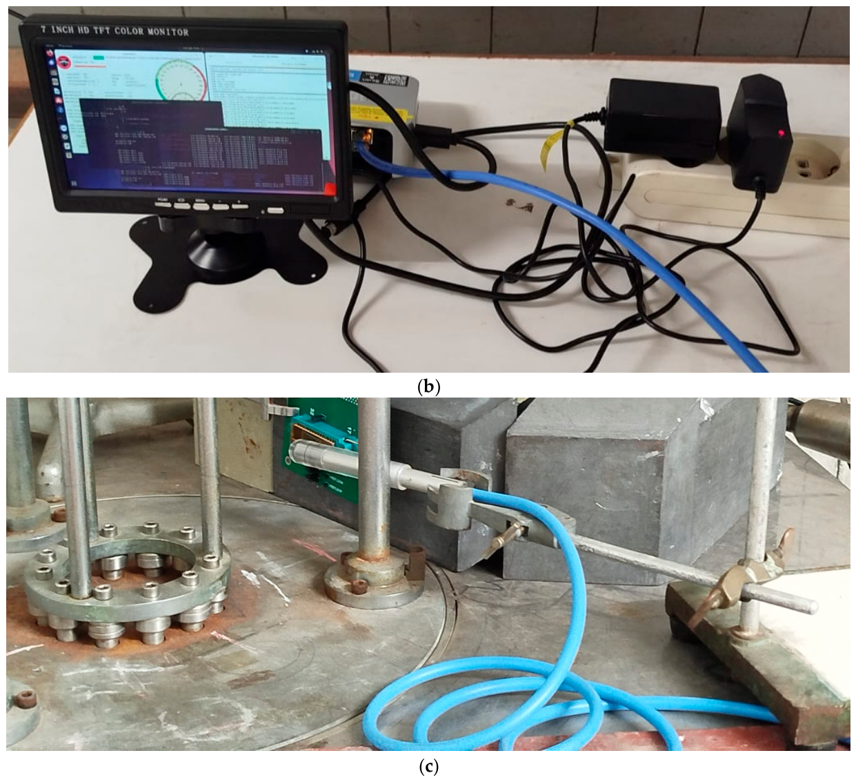
A PC running the Leonida Platform for overall control of the testing campaign was placed in the Warm Chamber and connected to MB using a USB cable, as shown in
Figure 35b; finally, the PC was connected via Ethernet outside the Warm Chamber directly to the control room (Cold Chamber), where a hub guaranteed a connection inside the facility and also from outside via the internet.
Dosimetry was performed before the TID campaign by dose rate measurement (
Figure 35c) and irradiation time monitoring. The Unidos-E dosimeter and TM 30013 ionization chamber, both from PTW Freiburg, were used for dose rate measurement.
During the experiment for the TID measures we used a 0.8 rad/s dose rate reaching up to 1 Mrad (Si) with no significant degradation in terms of electrical performance (output voltage and power consumption). No failures were observed in the test setup (the motherboard was fully functional at the end of the experiment) with the adopted approach. We would like to mention that the BGR alone was characterized as well. A complete view of the relevant results can be found in [
22], but it is worth underlining that the irradiation was extended up to 1 Mrad (Si) without any significant degradation with respect to pre-rad values.
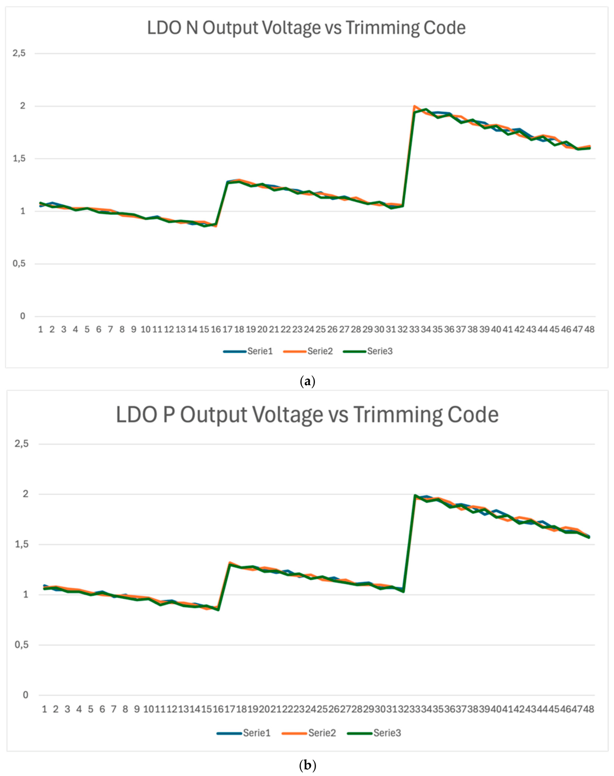
As a first test, we measured the LDO output voltage as a function of the BGR trimming code (the 0.9 V BGR output voltage is used as reference for the LDO). The measure was repeated for the three programmable output voltages: 1 V, 1.2 V and 1.8 V. The voltage was converted by the ADC (12-bit) onboard in Arduino Due
® and the code was then recorded to a file by Leonida Platform.
Figure 36a,b show the LDO NMOS and LDO PMOS output voltage, where Serie1 is pre-rad, Serie2 is at 300 krad (Si) and Serie3 at 1 Mrad (Si). Also considering the inaccuracy of measurements, the output of the LDO NMOS did not change significantly.
To have a clear view of the induced variation, we focused on the code that most closely approximates the nominal output value. For example, in
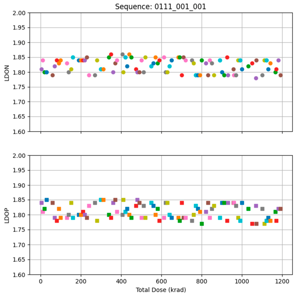
Figure 37, the 1.8 V (code 0111) is shown as a function of the TID. The variation is in the order of 50 mV (<3%) over > 1Mrad (Si) dose range and is mainly determined by setup and measure inaccuracy.
We have also recorded the static power consumption, due mainly to the analog part, as read by the current sense circuit placed on the shield board. It generates a voltage that is proportional to the supply current flowing across it. Its value is then converted by the Arduino Due
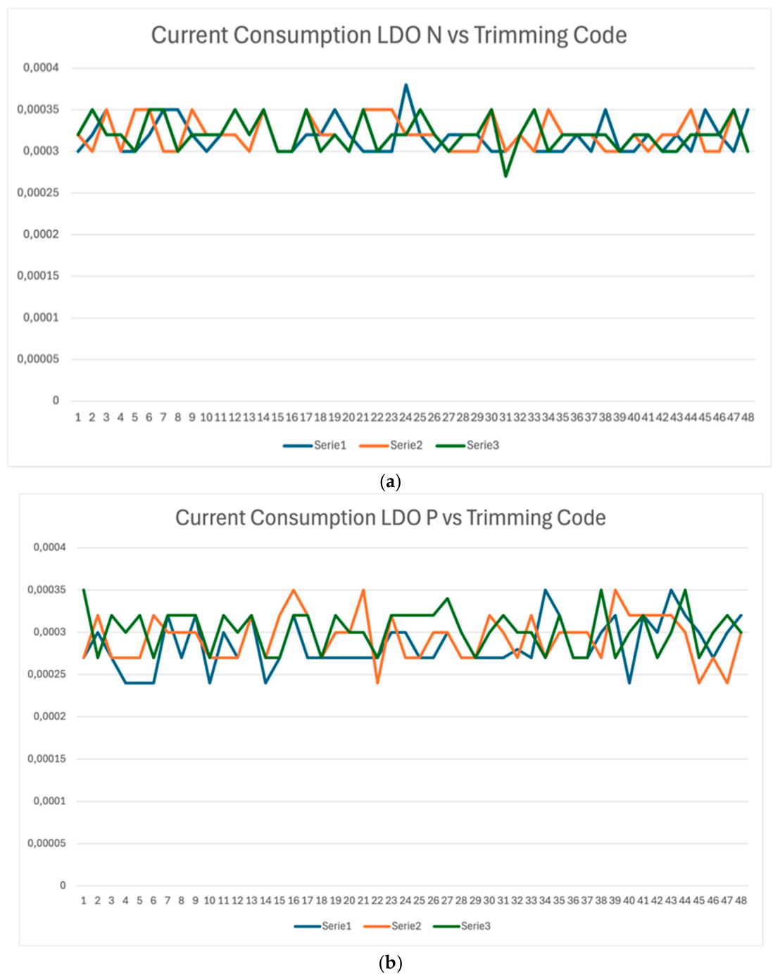
® ADC and recorded by Leonida Platform. The measured analog current consumption in mA is shown in
Figure 38 for LDO NMOS (a) and for LDO PMOS (b) where Serie1 is pre-rad, Serie2 is at 300 krad and Serie3 at 1 Mrad. As can be seen, apart an uncertainty in the measure (due to low-voltage drop on current sense, ADC finite resolution, and noise) it is almost constant between 0.3 mA and 0.35 mA (NMOS), 0.25 mA and 0.35 mA (PMOS), and up to 1 Mrad (Si).
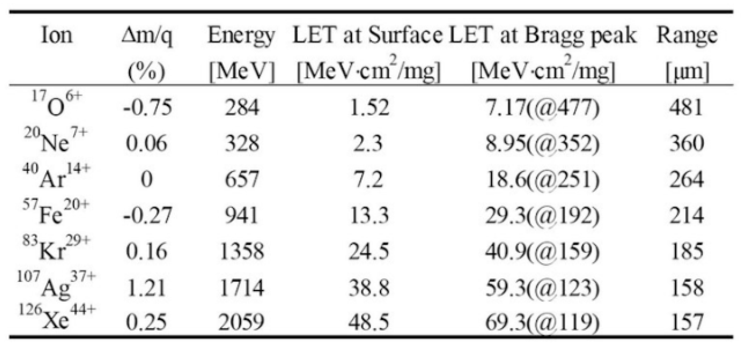
Regarding SEE (single-event effect) tests, the authors performed a campaign on both BGRs and LDOs with heavy ions at the RADEF Facility (University of Jyvaskyla, Finland).
Since during a previous campaign carried out in 2025 it was clear that no SELs and no SETs were triggered using low-energy ions, the focus in this chip has been on those ions offering the highest LET, as shown in
Figure 39, and more specifically on Xe and Ag.
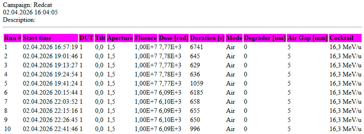
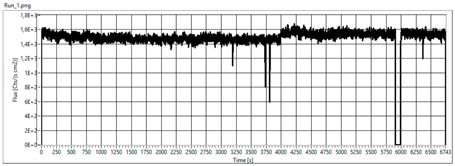
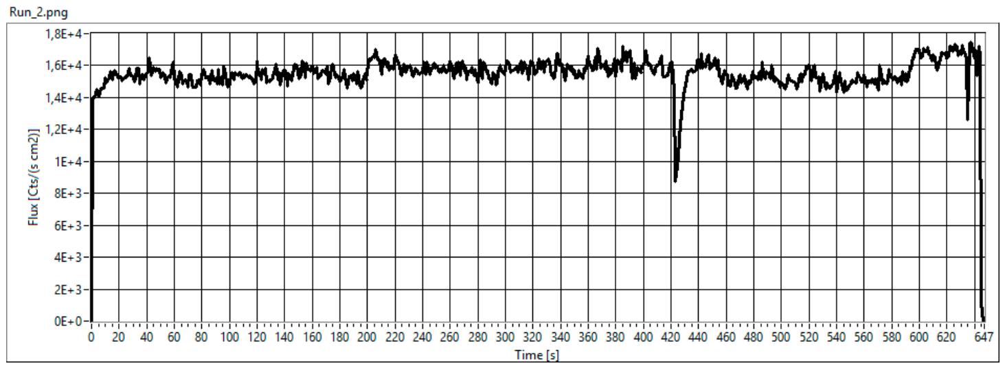
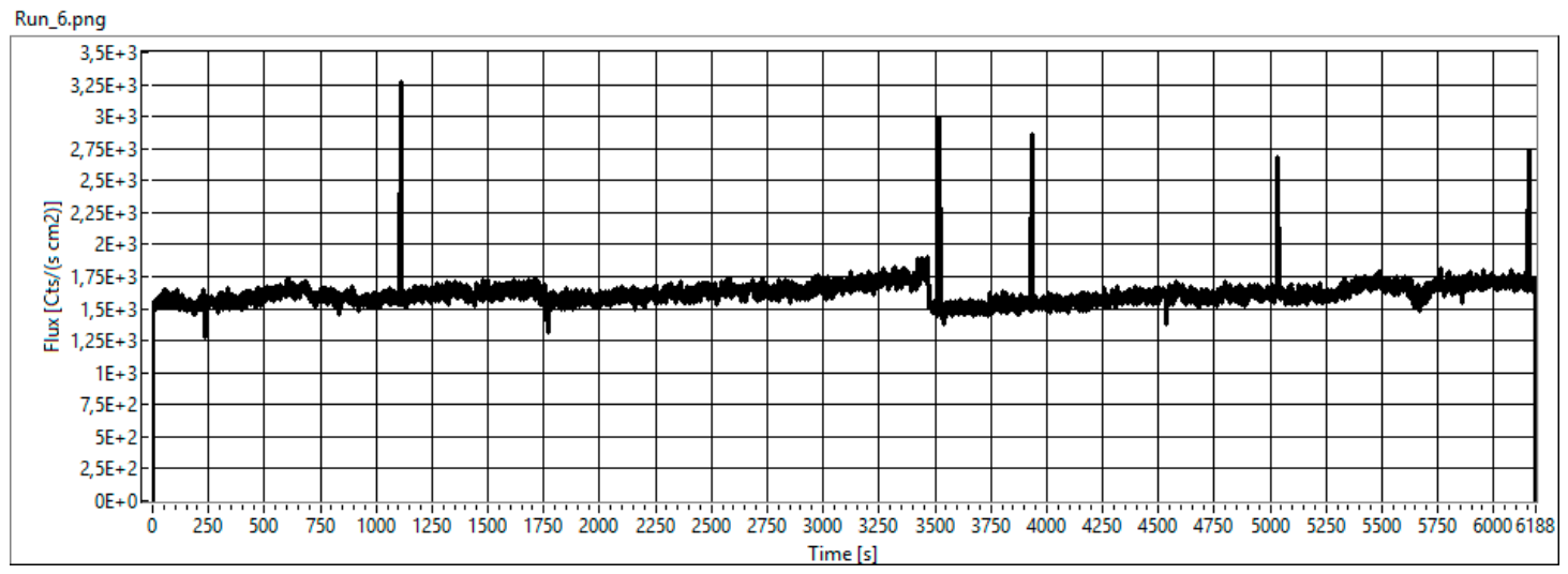
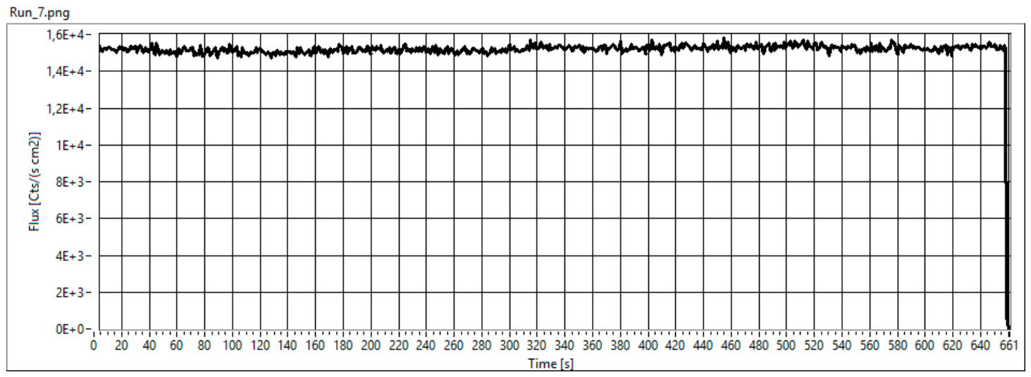
Three DUTs have been irradiated both with Xe (first run) and Ag (second run) using three different fluxes, as shown in
Table 4.
The overview of the campaign is summarized in
Figure 40, where key data (including dose) are presented.
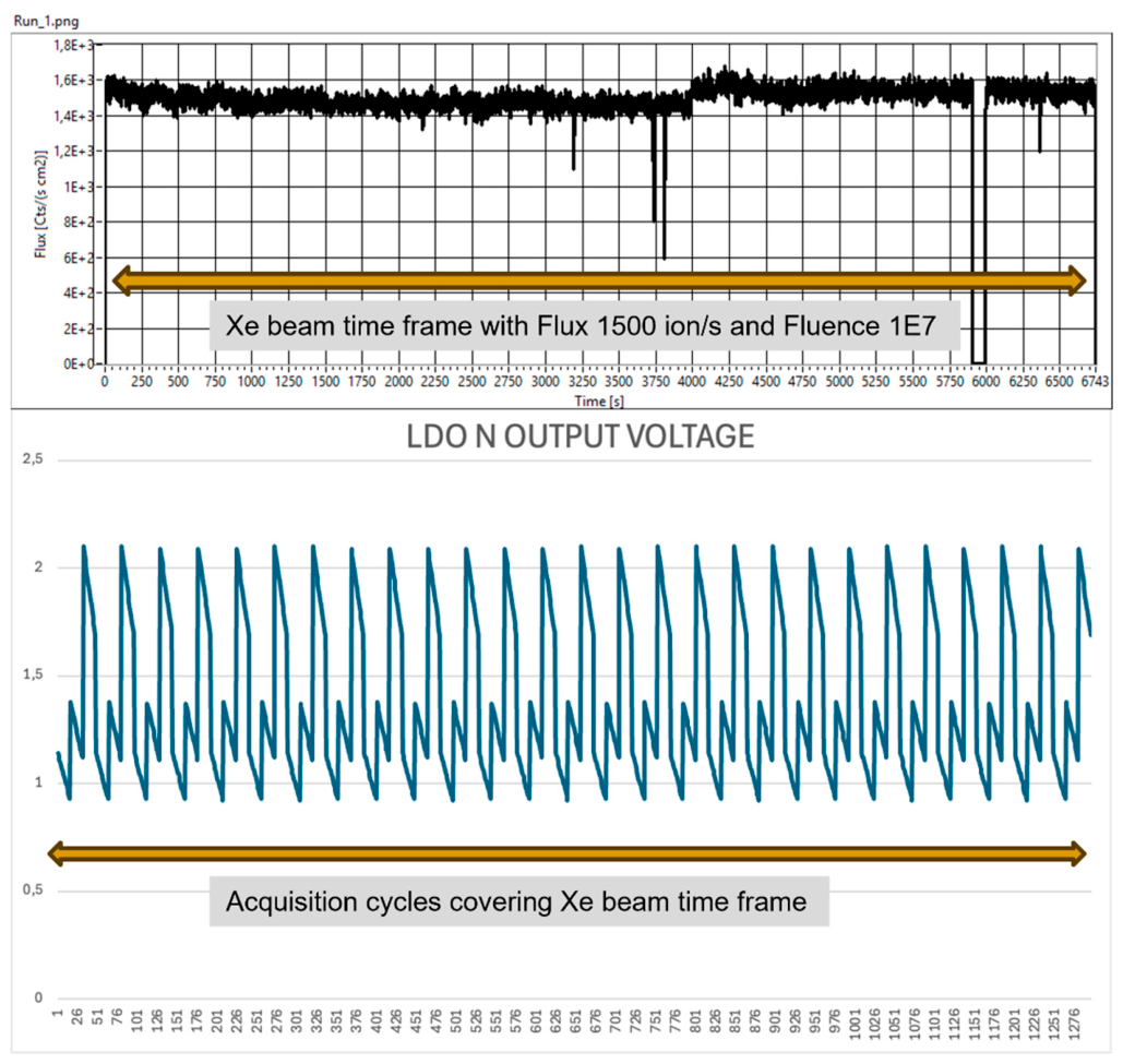
The rationale of the campaign was to start irradiation with Xe (the most energetic available with this cocktail) using three different fluxes (1500 ion/s, 15,000 ion/s and 10,000 ion/s) and keeping the fluence constant at 1 × 10
7 ions; of course, with lower fluxes, reaching the target fluence took more time than using higher fluxes, as shown in
Figure 41,
Figure 42,
Figure 43 and
Figure 44, and since during the first run all DUTs survived in the second run, Ag ions were used, thus making only one ion change on the beam (usually the ion change takes half an hour).
In the second run, one DUT (#105) originally tested with low-flux Xe ions was irradiated with medium-flux Ag and vice versa for DUT #106 (medium flux with Xe on low flux with Ag). One DUT (#106) was irradiated with high flux both with Xe and Ag (15,000 ion/s).
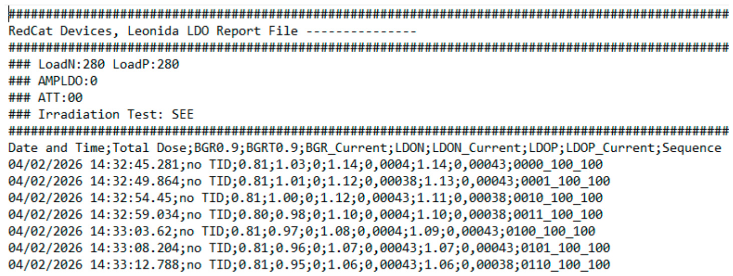
For every, run data was acquired automatically and stored in a data file in order to be elaborated after the test. The report is structured as shown in
Figure 45 where the bandgap reference voltage (with and without trimming) and bandgap reference current (for both), LDO voltage, and current (both N and P) are stored with the corresponding sequence. In this way, all possible combinations (1.8 V, 1.2 V and 1.0 V) using all trimming options could be checked during the test.
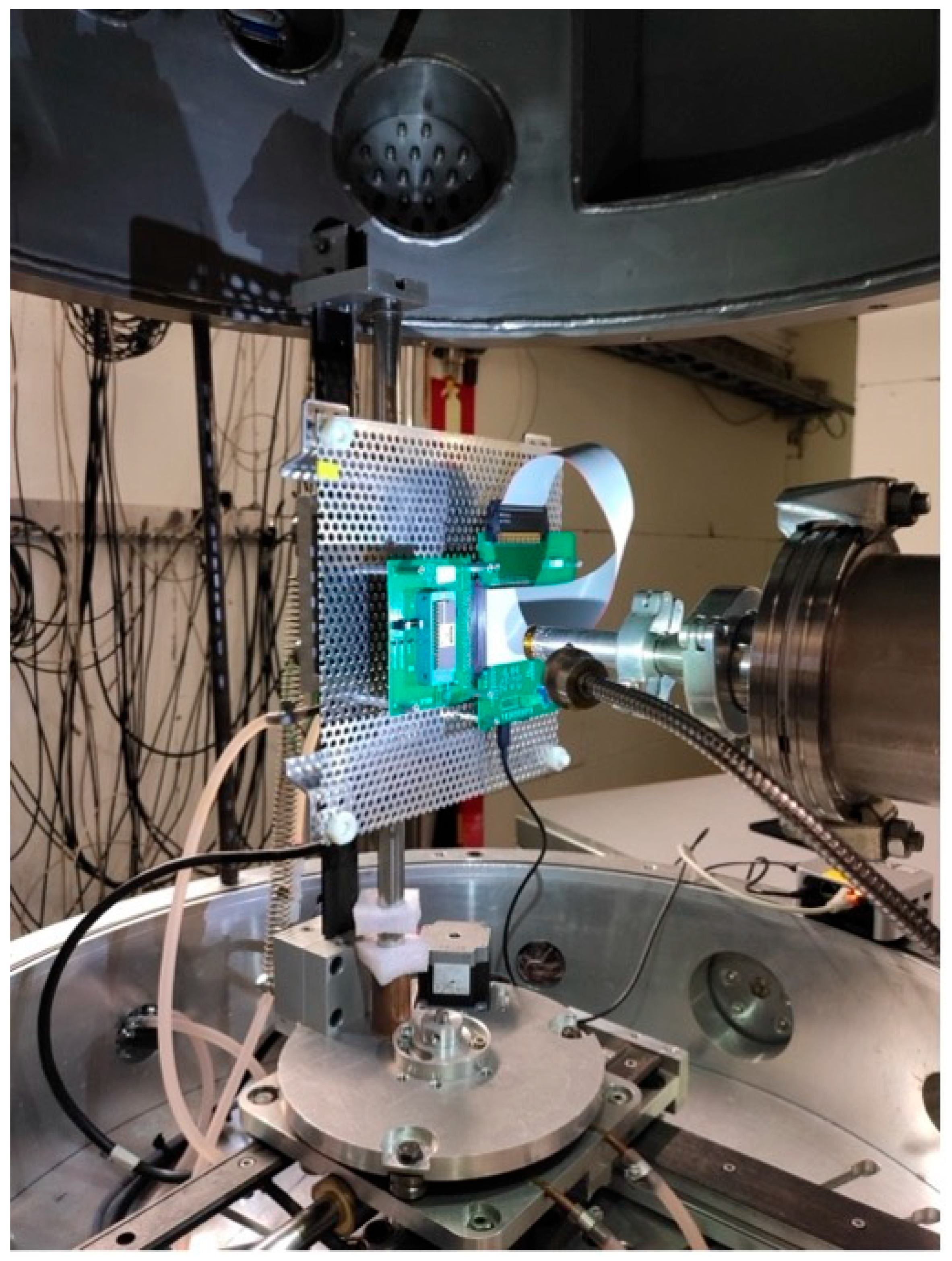
As already mentioned, since the beam is very collimated, it was not necessary to shield the motherboard as done in the TID test (
Figure 46). Thus, the experiment was controlled both in the facility control room and remotely. The former is needed to check that the Leonida software package was functional and to monitor the parameters of the beam. The latter is the Leonida Platform software package for the control of the test.
It is worth describing the developed software as well. For LDO testing, the Leonida Platform is structured in two layers. The lower layer is based on the Arduino IDE
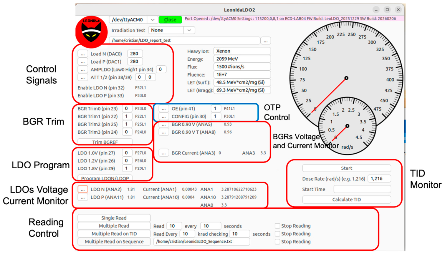
® environment and communicates directly with the Arduino board through a USB connection. The upper layer, developed in a BASIC-like language (Gambas3) and managed through a graphical user interface (GUI), provides test control and data visualization. The Leonida Platform GUI, shown in
Figure 47, supports the characterization of both BGRs and LDOs. Its main functions can be grouped into different categories: control signals, BGR trim, LDO Program, measurement sections, and reading control. The control signals, BGR trim, LDO Program allow for the user to configure the active load current (100 μA, 10 mA, or 20 mA) for LDO testing, as well as to program the trimming bits of the bandgap reference and the output voltage of the LDO. The measurement sections display the measured BGR output voltages, LDO output voltage, and current consumption. Finally, the reading control section manages data acquisition, either as a single-shot measurement or as periodic measurements performed at predefined irradiation intervals. A special section (blue line) is devoted to OTP programming. Additional information, including dose rate and accumulated TID, is displayed in the lower-right area of the GUI, while the file name used for data storage can be specified at the top center of the interface.
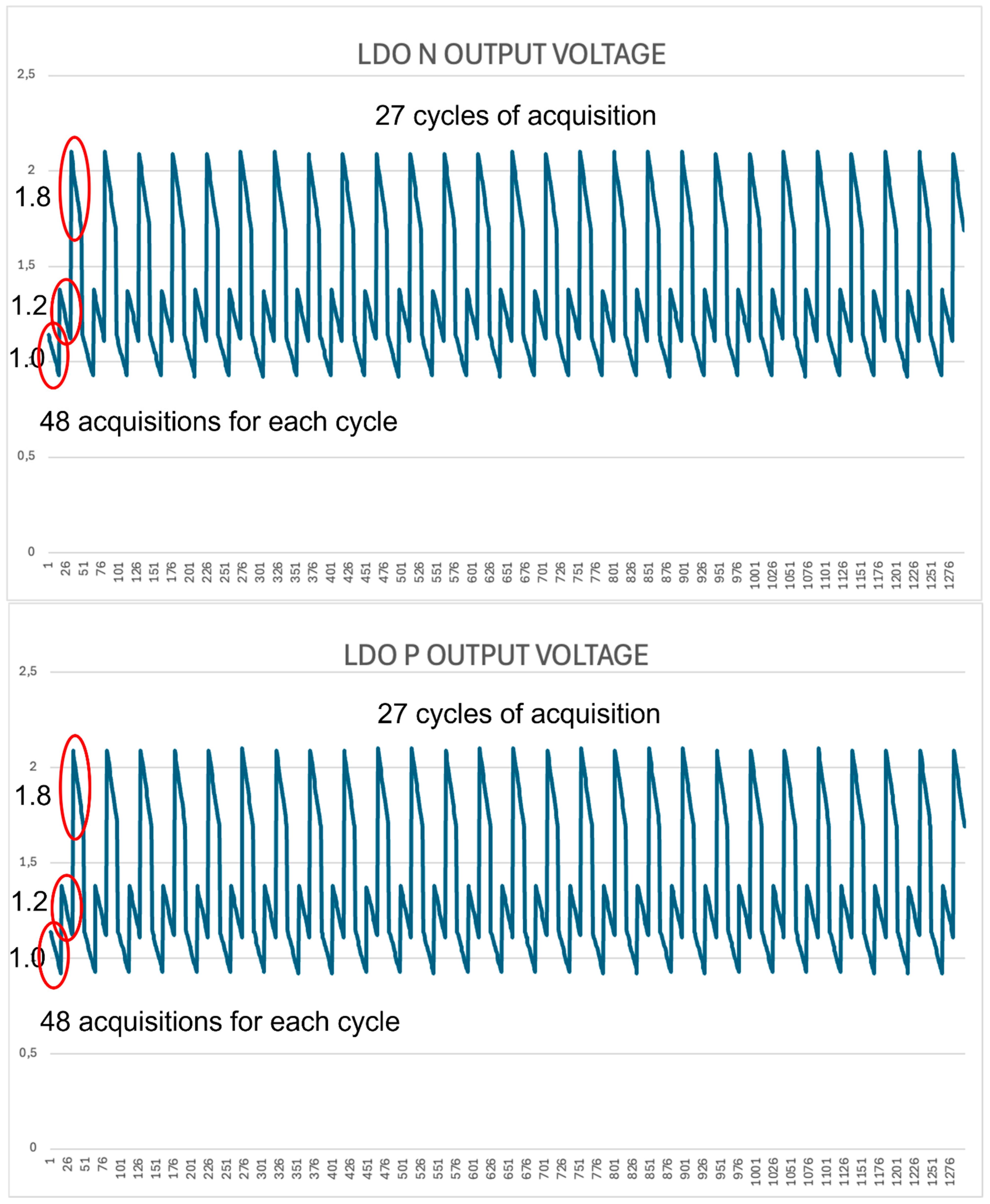
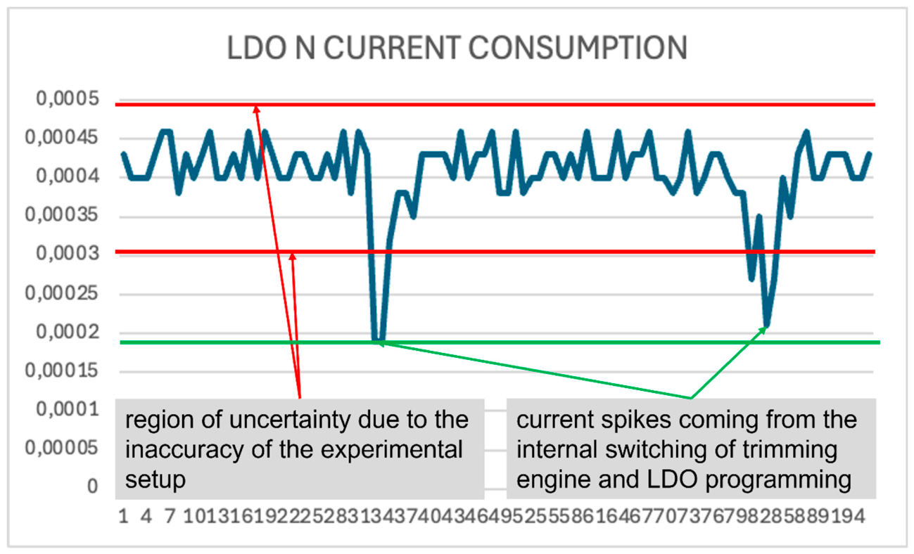
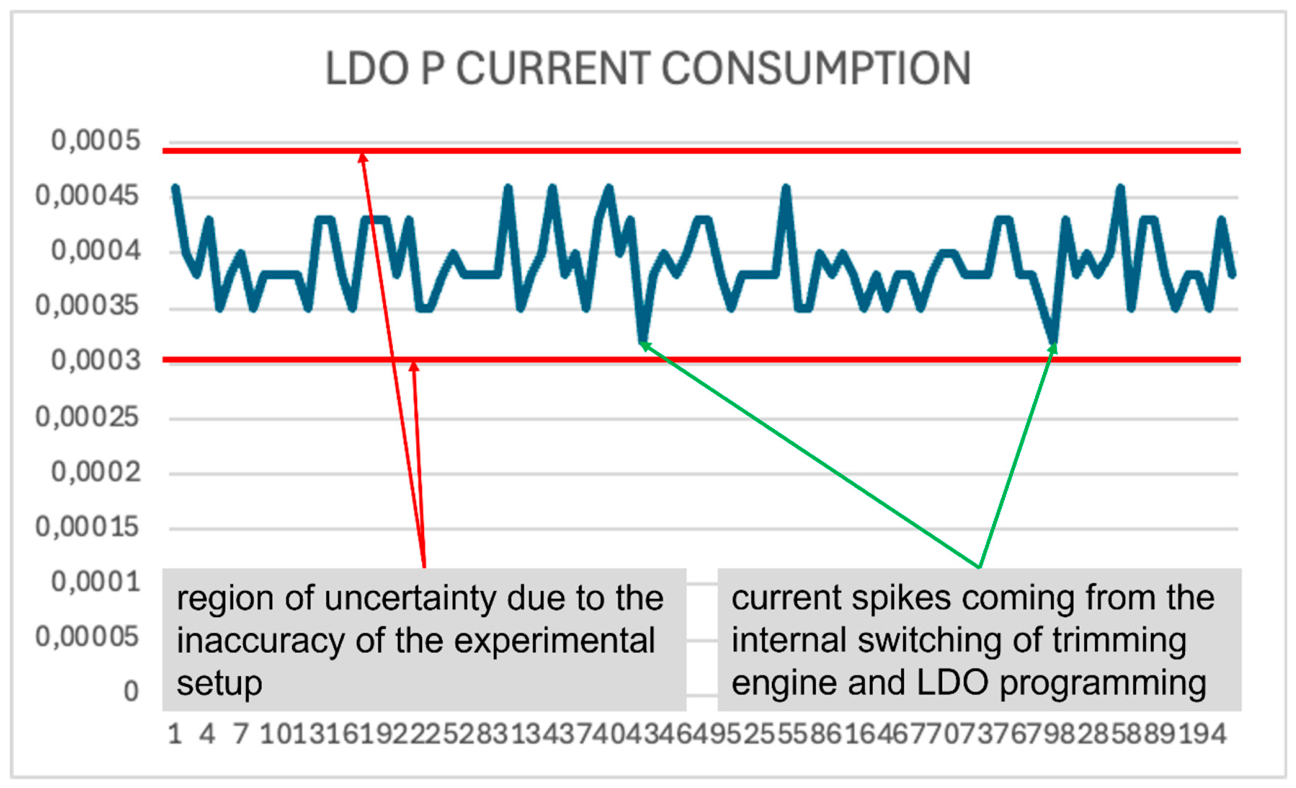
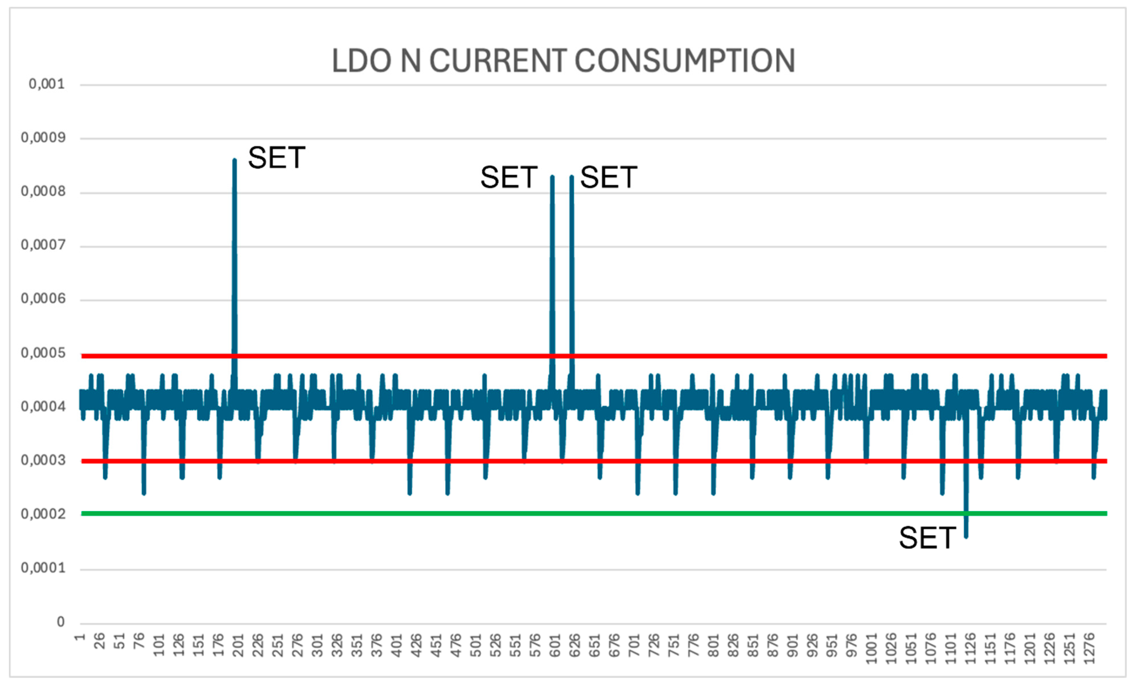
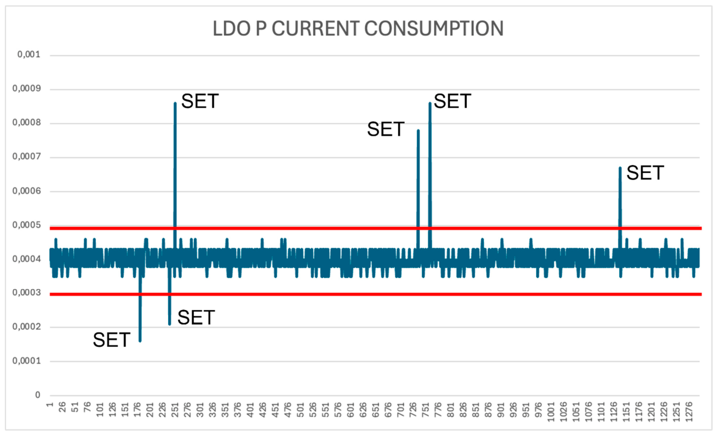
Data analysis showed that from the point of view of the output node of the LDO (both N and P) there are not SELs; for each run, several acquisition cycles have been carried on; each cycle consists of 48 acquisitions covering both LDO N and P in 1.8 V, 1.2 V and 1.0 V configuration and all possible trimming options has been tested. So, since the trimming consists of four bits, there are 16 acquisitions for each LDO configuration (3), and this leads to 48 (16 × 3) elementary acquisitions.
Figure 48 shows the full set of acquisitions consisting of 27 cycles (each having 48 elementary acquisitions); this number (27) comes from the length of the beam run to reach 1 × 10
7 ions of fluence using 1500 ion/s as flux. Of course, at the beginning and at the end of the beam run, some cycles were skipped, since the board was not synchronized with the beam but started and stopped manually.
More in detail, each acquisition cycle (see
Figure 49) does not show any bump or peak in LDOP or LDON; this means that output voltages are stable during the entire run of Xe ions but of course this does not mean there are not transients during the time frame (6743 s); they simply do not reach the output voltage.
To check the internal behavior of the LDO (both N and P), current measurement is one of the main approaches because it considers not only the output MOS but also the bandgap reference, the operational amplifier and the circuitry driving the switches connected to poly resistors for achieving the trimming operation.
Of course, current measurements must consider values around 400 uA, and deviations are expected because of the setup equipment suffering a flat cable connection between the motherboard and daughterboard and the limitation coming from the internal ADCs provided by Arduino Due; indeed, 400 uA will be something between 300 uA and 500 uA, so delimiting a region of uncertainty as shown between red lines in
Figure 50, where a couple of cycles run with no heavy ions. Moreover, the test has be carried out changing the LDOs’ configuration (1.8 V, 1.2 V and 1.0 V) and exploring all trimming options; this leads to a continuous configuration passage where switches play a role and the LDOs are forced to adapt themselves, creating leverage on the internal feedback loop in the operational amplifier.
According to the boundary regions described in
Figure 50, where current spikes can be attributed to the experimental setup, it is possible to discard known spikes from other current spikes clearly coming from heavy ion energy release.
Figure 51 shows the current measurements along the entire beam run of both the LDON and LDOP, and spikes exceeding the boundary regions described in
Figure 50 can be attributed to transients in critical nodes of the LDO or power supply pads.
The reason why these SETs are evident in power consumption measurements and not in the LDOs’ output voltage is in line with the intrinsic nature and the internal architecture of these devices. The feedback loop (see
Figure 1) handles the transients exactly like any other disturbance affecting the LDO; as a matter of fact, voltage regulators are used to provide stable power supplies to other components, thus acting as filters between DC-DC converters and units to be supplied (e.g., ADC, DAC requiring stable power); the current injections coming from heavy ion energy release are seen and filtered exactly like disturbances coming from power lines.
Table 5 summarizes the LDOs’ measured performance.
For a clearer comparison with previously reported radiation-hardened LDO implementations,
Table 6 summarizes the main design parameters and performance metrics of the proposed regulators and representative state-of-the-art solutions.
Recent research on radiation-tolerant LDOs has addressed different aspects of circuit performance and radiation robustness. Fan et al. [
16] presented a fast-transient radiation-hardened LDO in 0.6 μm BiCMOS technology, targeting high-current space applications and achieving up to a 6 A output current. Li et al. [
19] presented a 3.5 A LDO fabricated in a radiation-hardened 0.18 μm BCD process. Radiation-hard linear regulators have also been developed for high-energy physics applications, such as the multifunctional HV/LV regulator reported in [
18].
In contrast to these approaches, the present work focuses on the radiation-hard implementation of conventional NMOS and PMOS pass device LDO architectures in standard 180 nm CMOS technology. The two architectures are implemented under comparable design conditions and experimentally characterized both before and after irradiation. The work therefore focuses on the effectiveness of circuit- and layout-level radiation-hardening techniques and on the comparison of the radiation response of the two pass transistor architectures. In particular, the demonstrated operation beyond 1 Mrad(Si) and the absence of observed single-event latch-up up to approximately 60 MeV·cm2/mg provide an experimental assessment of the radiation robustness of the proposed implementations.